EP3610275B1 - Wafer-sondenkarte, analysevorrichtung damit und verfahren zur herstellung der wafer-sondenkarte - Google Patents
Wafer-sondenkarte, analysevorrichtung damit und verfahren zur herstellung der wafer-sondenkarte Download PDFInfo
- Publication number
- EP3610275B1 EP3610275B1 EP18809303.3A EP18809303A EP3610275B1 EP 3610275 B1 EP3610275 B1 EP 3610275B1 EP 18809303 A EP18809303 A EP 18809303A EP 3610275 B1 EP3610275 B1 EP 3610275B1
- Authority
- EP
- European Patent Office
- Prior art keywords
- pads
- probe card
- wafer
- electric wiring
- analysis apparatus
- Prior art date
- Legal status (The legal status is an assumption and is not a legal conclusion. Google has not performed a legal analysis and makes no representation as to the accuracy of the status listed.)
- Active
Links
Images




Classifications
-
- G—PHYSICS
- G01—MEASURING; TESTING
- G01R—MEASURING ELECTRIC VARIABLES; MEASURING MAGNETIC VARIABLES
- G01R31/00—Arrangements for testing electric properties; Arrangements for locating electric faults; Arrangements for electrical testing characterised by what is being tested not provided for elsewhere
- G01R31/26—Testing of individual semiconductor devices
- G01R31/2607—Circuits therefor
- G01R31/2632—Circuits therefor for testing diodes
- G01R31/2635—Testing light-emitting diodes, laser diodes or photodiodes
-
- G—PHYSICS
- G01—MEASURING; TESTING
- G01J—MEASUREMENT OF INTENSITY, VELOCITY, SPECTRAL CONTENT, POLARISATION, PHASE OR PULSE CHARACTERISTICS OF INFRARED, VISIBLE OR ULTRAVIOLET LIGHT; COLORIMETRY; RADIATION PYROMETRY
- G01J1/00—Photometry, e.g. photographic exposure meter
- G01J1/42—Photometry, e.g. photographic exposure meter using electric radiation detectors
-
- G—PHYSICS
- G01—MEASURING; TESTING
- G01J—MEASUREMENT OF INTENSITY, VELOCITY, SPECTRAL CONTENT, POLARISATION, PHASE OR PULSE CHARACTERISTICS OF INFRARED, VISIBLE OR ULTRAVIOLET LIGHT; COLORIMETRY; RADIATION PYROMETRY
- G01J3/00—Spectrometry; Spectrophotometry; Monochromators; Measuring colours
- G01J3/46—Measurement of colour; Colour measuring devices, e.g. colorimeters
- G01J3/50—Measurement of colour; Colour measuring devices, e.g. colorimeters using electric radiation detectors
- G01J3/505—Measurement of colour; Colour measuring devices, e.g. colorimeters using electric radiation detectors measuring the colour produced by lighting fixtures other than screens, monitors, displays or CRTs
-
- G—PHYSICS
- G01—MEASURING; TESTING
- G01R—MEASURING ELECTRIC VARIABLES; MEASURING MAGNETIC VARIABLES
- G01R1/00—Details of instruments or arrangements of the types included in groups G01R5/00 - G01R13/00 and G01R31/00
- G01R1/02—General constructional details
- G01R1/06—Measuring leads; Measuring probes
- G01R1/067—Measuring probes
- G01R1/06711—Probe needles; Cantilever beams; "Bump" contacts; Replaceable probe pins
- G01R1/06733—Geometry aspects
- G01R1/06744—Microprobes, i.e. having dimensions as IC details
-
- G—PHYSICS
- G01—MEASURING; TESTING
- G01R—MEASURING ELECTRIC VARIABLES; MEASURING MAGNETIC VARIABLES
- G01R1/00—Details of instruments or arrangements of the types included in groups G01R5/00 - G01R13/00 and G01R31/00
- G01R1/02—General constructional details
- G01R1/06—Measuring leads; Measuring probes
- G01R1/067—Measuring probes
- G01R1/073—Multiple probes
- G01R1/07307—Multiple probes with individual probe elements, e.g. needles, cantilever beams or bump contacts, fixed in relation to each other, e.g. bed of nails fixture or probe card
- G01R1/07314—Multiple probes with individual probe elements, e.g. needles, cantilever beams or bump contacts, fixed in relation to each other, e.g. bed of nails fixture or probe card the body of the probe being perpendicular to test object, e.g. bed of nails or probe with bump contacts on a rigid support
-
- G—PHYSICS
- G01—MEASURING; TESTING
- G01R—MEASURING ELECTRIC VARIABLES; MEASURING MAGNETIC VARIABLES
- G01R1/00—Details of instruments or arrangements of the types included in groups G01R5/00 - G01R13/00 and G01R31/00
- G01R1/02—General constructional details
- G01R1/06—Measuring leads; Measuring probes
- G01R1/067—Measuring probes
- G01R1/073—Multiple probes
- G01R1/07307—Multiple probes with individual probe elements, e.g. needles, cantilever beams or bump contacts, fixed in relation to each other, e.g. bed of nails fixture or probe card
- G01R1/0735—Multiple probes with individual probe elements, e.g. needles, cantilever beams or bump contacts, fixed in relation to each other, e.g. bed of nails fixture or probe card arranged on a flexible frame or film
-
- G—PHYSICS
- G01—MEASURING; TESTING
- G01R—MEASURING ELECTRIC VARIABLES; MEASURING MAGNETIC VARIABLES
- G01R3/00—Apparatus or processes specially adapted for the manufacture or maintenance of measuring instruments, e.g. of probe tips
-
- G—PHYSICS
- G01—MEASURING; TESTING
- G01J—MEASUREMENT OF INTENSITY, VELOCITY, SPECTRAL CONTENT, POLARISATION, PHASE OR PULSE CHARACTERISTICS OF INFRARED, VISIBLE OR ULTRAVIOLET LIGHT; COLORIMETRY; RADIATION PYROMETRY
- G01J1/00—Photometry, e.g. photographic exposure meter
- G01J1/42—Photometry, e.g. photographic exposure meter using electric radiation detectors
- G01J2001/4247—Photometry, e.g. photographic exposure meter using electric radiation detectors for testing lamps or other light sources
- G01J2001/4252—Photometry, e.g. photographic exposure meter using electric radiation detectors for testing lamps or other light sources for testing LED's
Definitions
- Example embodiments of the present disclosure relate to a wafer probe card for evaluating micro light emitting diodes (LEDs), an analysis apparatus including the same, and a method of fabricating the wafer probe card.
- LEDs micro light emitting diodes
- Light-emitting devices such as light-emitting diodes (LED) or vertical cavity surface emitting laser diode (VCSELs) are inspected to evaluate electrical and optical characteristics thereof after completing the manufacture thereof.
- LED light-emitting diodes
- VCSELs vertical cavity surface emitting laser diode
- a small electrified probe may be brought into direct contact with an LED provided on a wafer to supply a current to the LED such that the LED emits light.
- An analysis system may acquire electrical and optical properties of light emitted from each LED provided on the wafer in the form of Blue Tape data.
- manufacturers of high-brightness LED devices separate the LEDs from the wafer and supply the LEDs in accordance with wavelength and brightness required in a manufacturing process.
- LED devices including sapphire provided on a wafer may be larger in size, the LED devices may be sufficiently inspected by using the probe.
- each LED is becoming smaller to several tens of micrometers ( ⁇ m) in size.
- EP1837663A1 discloses an inspection contact structure to contact with an object electrically to be inspected to inspect electric properties of the object to be inspected, and a probe card.
- US7948252B2 discloses a method of designing and manufacturing a probe card assembly.
- US9222961 B1 discloses a vertical probe card and a method for manufacturing the same.
- WO2009147718A1 discloses a method of manufacturing the probe wafer.
- US8476918B2 discloses a semiconductor test system.
- One or more example embodiments of the present disclosure provide a wafer probe card that matches in one-to-one correspondence with an LED wafer by implementing a probe system having the same size as the LED wafer and inspects brightness and wavelength of a plurality of LEDs at once by controlling the plurality of LEDs to emit light, an analysis apparatus including the same, and a method of fabricating the wafer probe card.
- a probe card for a wafer including a substrate, an insulating layer formed on the substrate, a plurality of first pads and a plurality of second pads formed on the insulating layer, and a plurality of rear pads respectively connected to the plurality of first pads and the plurality of second pads via through silicon vias (TSVs), wherein the plurality of first pads and the plurality of second pads are configured to transfer electrical signals to electrode pads of a light emitting diode (LED) wafer.
- TSVs through silicon vias
- the plurality of first pads are connected to each other in a line-by-line manner by an electric wiring in a first direction, the electric wiring connecting the first pads being connected to the TSVs connecting the first pads and rear pads, and the plurality of second pads are connected to each other in a line-by-line manner by an electric wiring in a second direction, the electric wiring connecting the second pads being connected to the TSVs connecting the second pads and rear pads.
- the plurality of first pads are formed by etching the insulating layer provided with the plurality of first pads and re-depositing the plurality of first pads after depositing the plurality of second pads.
- the substrate may be formed of silicon.
- the wafer probe card may include holes for alignment with the LED wafer.
- An anisotropic conductive film (ACF) and a polyimide (PI) film may be formed on the plurality of rear pads.
- an analysis apparatus including an optical source application unit configured to transmit power to a wafer probe card;
- the processor may be further configured to control the optical source application unit to alternately apply the power.
- the processor may be further configured to create map data on the plurality of LEDs based on the measurement results, and the analysis apparatus may be further comprise a storage unit configured to store the created map data.
- the processor may be further comprise a stage on which a wafer comprising the plurality of LEDs is placed, wherein the stage may be comprise a glass window configured to transmit emitted light, and the optical measurement unit may be further configured to collect light passing through the glass window.
- a method of fabricating a probe card for a wafer including preparing a substrate having an insulating layer formed to expose a plurality of first pads, forming a plurality of second pads on the insulating layer; and forming a plurality of rear pads formed on a surface opposite to a surface of the substrate provided with the insulating layer, wherein the plurality of rear pads are connected to the plurality of first pads and the plurality of second pads using through silicon vias (TSVs), wherein the plurality of first pads are connected to each other in a line-by-line manner by an electric wiring in a first direction, the electric wiring connecting the first pads being connected to the TSVs connecting the first pads and rear pads ,
- TSVs through silicon vias
- the method may further include leveling the plurality of first pads and the plurality of second pads.
- the method may further include forming an anisotropic conductive film (ACF) to the plurality of rear pads, and forming a polyimide (PI) film on the ACF.
- ACF anisotropic conductive film
- PI polyimide
- the wafer probe card may match in one-to-one correspondence with the LED wafer by implementing a probe system having the same size as the LED wafer and inspect brightness and wavelength of a plurality of LEDs at once by controlling the plurality of LEDs to emit light.
- FIG. 1 is a schematic diagram illustrating an analysis apparatus including a wafer probe card according to an example embodiment.
- an analysis apparatus 1 may include a wafer probe card 100, an optical source application unit 30 configured to apply a current or voltage to the wafer probe card 100, a light-emitting diode (LED) wafer 200 configured to emit light upon receiving the current or voltage from the wafer probe card 100, a glass window 51 configured to transmit light emitted from LEDs included in the LED wafer 200, an optical measurement unit 70 configured to measure wavelength or brightness of light emitted from the LEDs included in the LED wafer 200, and a controller 90 configured to create map data based on signals received from the optical measurement unit 70 and control the overall operation of the analysis apparatus 1.
- LED light-emitting diode
- the wafer probe card 100 may be provided in the same size as the LED wafer 200 to correspond to the LED wafer 200 and may transfer a current or voltage to the LED wafer 200 through pads 110 and 130 as illustrated in FIG. 3 .
- the LED wafer 200 is a target object to be analyzed by the analysis apparatus 1 and placed on a stage 50 of the analysis apparatus 1.
- the LED wafer 200 includes LEDs of a predetermined size which includes electrode pads 210 and 230 as illustrated in FIG. 3 which may be brought into contact with the pads 110 and 130 of the wafer probe card 100, respectively.
- the optical source application unit 30 may transmit a voltage or current to the wafer probe card 100 in accordance with a control signal of the controller 90 and is connected specifically to a polyimide (PI) film 170 as illustrated in FIG. 20 included in the wafer probe card 100.
- PI polyimide
- the optical measurement unit 70 may receive light emitted from the LEDs and transmit the measurement results to the controller 90. Specifically, the optical measurement unit 70 may measure an amount of the emitted light and collect a spectrum of light. The optical measurement unit 70 may convert the received light into an electrical signal by analyzing brightness or wavelength of the received light and may transmit the electrical signal to the controller 90.
- the controller 90 may be a processor configured to control the overall operation of the analysis apparatus 1. Particularly, the controller 90 may control the optical source application unit 30, the optical measurement unit 70, and the stage 50, and output map data including evaluation results of the LEDs created by receiving the measurement results from the optical measurement unit 70.
- the controller 90 may be implemented using a memory to store data on algorithms for controlling operations of the elements of the analysis apparatus 1 or programs for realizing the algorithms and a processor to perform the operations by using data stored in the memory.
- the memory and the processor may be implemented using separate chips or integrated into a single chip.
- the controller 90 may be connected to a storage unit configured to store the processed data.
- the storage unit may be implemented using at least one of a nonvolatile memory such as read only memory (ROM), programmable ROM (PROM), erasable programmable ROM (EPROM), electrically erasable programmable ROM (EEPROM), and flash memory, a volatile memory such as random access memory (RAM), or a storage medium such as hard disk drive (HDD) and CD-ROM, without being limited thereto.
- the storage unit may be a memory implemented as a separate chip from the processor described above with reference to the controller 90 or a memory integrated with the processor as a single chip.
- the analysis apparatus 1 may further include one or more elements in addition to the elements illustrated in FIG. 1 , or at least one of the elements illustrated in FIG. 1 may be excluded therefrom.
- the analysis apparatus 1 may further include an interface configured to output data processed by the controller 90 and receive an input command of a user, and a communication module configured to transmit the processed data to an external device.
- the interface may be connected to a display configured to display the map data created by the controller 90.
- the display may be implemented using a cathode ray tube (CRT), a digital light processing (DLP) panel, a plasma display penal (PDP), a liquid crystal display (LCD) panel, an electro luminescence (EL) panel, an electrophoretic display (EPD) panel, an electrochromic display (ECD) panel, a light emitting diode (LED) panel, or an organic light emitting diode (OLED) panel, without being limited thereto.
- CTR cathode ray tube
- DLP digital light processing
- PDP plasma display penal
- LCD liquid crystal display
- EL electro luminescence
- EPD electrophoretic display
- ECD electrochromic display
- LED light emitting diode
- OLED organic light emitting diode
- the interface may be connected to a hardware device such as a button, a switch, a pedal, a keyboard, a mouse, a track-ball, a lever, a handle, and a stick which receive input commands of the user and a software device such as a graphic user interface (GUI), for example, a touch pad which connects a touch signal of the user together with the display.
- GUI graphic user interface
- FIG. 2 is a view comparing a wafer probe card 100 and an LED wafer 200 according to an example embodiment.
- the LED wafer 200 may include one or more LEDs 250.
- Two electrode pads 210 and 230 corresponding to P and N types are provided on each LED 250.
- the P type electrode pad is referred to as a first LED electrode pad 210
- the N type electrode pad is referred to as a second LED electrode pad 230.
- the wafer probe card 100 includes a first pad 110 and a second pad 130 to transfer a current or voltage respectively to the first LED electrode pad 210 and the second LED electrode pad 230 in direct contact therewith.
- the wafer probe card 100 may include the first pads 110 and the second pads 130 in the same number and same size as the first and second LED electrode pads 210 and 230 of the LEDs 250 provided on the LED wafer 200 to be inspected.
- all of the LEDs 250 may be simultaneously inspected by applying a current or voltage to the LEDs 250 by using the wafer probe card 100. Therefore, efficiency of the inspection may be increased according to an example embodiment.
- FIGs. 3A and 3B are views for describing the operation of analysis apparatuses including different wafer probe cards according to example embodiments.
- the optical source application unit 30 may transmit a current or voltage required for inspection of the first pad 110 and the second pad 130 of the wafer probe card 100 based on the control of the controller 90.
- the wafer probe card 100 may transfer the voltage or current to the first LED electrode pad 210 and the second LED electrode pad 230 provided on the LED wafer 200 through the first pad 110 and the second pad 130, respectively.
- the LED 250 may emit light upon receiving power from each of the first and second electrode pads 210 and 230.
- Light emitted from the LED 250 may be transferred to the optical measurement unit 70 through the glass window 51 provided in the stage 50 and the optical measurement unit 70 collects the emitted light and analyzes brightness or wavelength of the light emitted from the LED 250.
- an optical measurement unit 70 included in an analysis apparatus 1 may be disposed in the same direction as the optical source application unit 30 with respect to the wafer probe card 100.
- Light may be emitted from the LED 250 not in a particular direction, and thus, the light emitted from the LED 250 may be reflected by the stage 50.
- the wafer probe card 100 may include a silicon substrate on which the first pad 110 and the second pad 130 are mounted. Thus, light emitted from the LED 250 may be reflected by the first pad 110 and the second pad 130.
- a wafer probe card 100 according to an example embodiment as illustrated in FIG. 3B may include through silicon vias (TSVs) 150 and may transmit light emitted from the LED 250 at predetermined intervals.
- TSVs through silicon vias
- the optical measurement unit 70 provided in the analysis apparatus 1 may collect light passing through the wafer probe card 100 of FIG. 3B and transfer the light to the controller 90.
- FIGs. 3A and 3B schematically illustrate examples of the present disclosure, but example embodiments are not limited thereto.
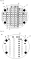
- FIGs. 4A and 4B are top and bottom views of a wafer probe card 100 according to an example embodiment.
- FIG. 4A illustrates a bottom surface 101 of the wafer probe card 100 and FIG. 4B illustrates a top surface 102 of the wafer probe card 100.
- the structure of the wafer probe card 100 may include the first pad 110 and the second pad 130 which are in one-to-one correspondence with the first LED electrode pad 210 and the second LED electrode pad 230 provided on the LED wafer 200 to be inspected.
- the first pad 110 and the second pad 130 may have the same size.
- the wafer probe card 100 has align holes 190 for the purpose of alignment with the LEDs and the LED wafer 200.
- the align holes 190 are formed in the bottom surface 101 and the top surface 102 of the wafer probe card 100, the align holes 190 are penetrated through the wafer probe card 100. The user may prevent the LED wafer 200 in contact with the wafer probe card 100 from being dislocated by using the align holes 190.
- one first pad 110 is connected with another first pad 110 in a longitudinal direction (first direction) in a line-by-line manner via an electric wire.
- one second pad 130 is connected to another second pad 130 in a lateral direction (second direction) via an electric wire.
- the electric wiring connecting the first pads 110 and the electric wiring connecting the second pads 130 are connected to TSV points 115 and 135 which are finally connected to an upper surface of the wafer probe card 100.
- the TSV points 115 and 135 are the through silicon vias (TSVs).
- the TSV points 115 and 135 are pathways through which the first pad 110 and the second pad 130 are connected to the top surface and the bottom surface.
- the TSV points 115 and 135 correspond to positive and negative poles of the power delivered by the optical source application unit 30. That is, the wafer probe card 100 may apply the current or voltage selectively to the first pads 110 and the second pads 130 of the wafer probe card 100 by controlling only the TSV points 115 and 135, and without connecting each of the first pads 110 and the second pads 130 with the positive and negative poles of the optical source application unit 30 in a one-to-one correspondence manner with each other.
- the current or voltage may be applied to a first TSV point 115 indicated by the reference numeral 115 in FIG. 4A and a second TSV point 135 in a second row from the last row and a column indicated by the reference numeral 135 of FIG. 4A
- first and second pads 110 and 130 may allow all LEDs 250 provided on the LED wafer 200 to emit light simultaneously, it is possible to omit separation/realignment processes performed by the conventional analysis apparatuses and it is possible to shorten an analysis time since a device for moving the analysis apparatus 1 such as a chuck is not required.
- holes 155 are formed as TSVs between the first pads 110 and the second pads 130.
- the holes 155 may be filled with a conductive metal on the top surface 102 of the wafer probe card 100.
- FIG. 5 is a view for describing an operating method of a wafer probe card 100 according to an example embodiment.
- a wafer probe card 100 may alternately apply negative power and positive power to the first TSV point 115 and the second TSV point 135 in a manner different from the example embodiment described above with reference to FIGs. 4A and 4B .
- diodes illustrated in FIG. 5 correspond to the first pads 110 and the second pads 130 respectively.
- a negative power is applied to a first gate G1 and a positive power is applied to a first source S1.
- a positive power is applied to the first gate G1 and a negative power is applied to the first source S1.
- two LEDs may emit light by using one wiring by alternately applying positive and negative powers by the optical source application unit 30.
- FIG. 6 is a flowchart for describing a method of fabricating a wafer probe card according to an example embodiment.
- FIGs. 7 to 20 are diagrams for describing the method of fabricating the wafer probe card.
- a method of fabricating the wafer probe card 100 includes coating a photoresist 400 on a silicon wafer 105 as illustrated in FIG. 7 (300).
- the photoresist 400 is etched to correspond to a position of the first pad 110 in accordance with the number of pixels (310).
- a mask 500 corresponding to the position of the first pad 110 is used to form the first pad 110.
- the photoresist 400 is exposed to light by using an exposure unit as illustrated in FIG. 8 and etched as illustrated in FIG. 9 .
- the first pad 110 is deposited thereon and an insulating material is coated thereon to form an insulating layer 106 as illustrated in FIG. 11 (320).
- the first pad 110 is formed on an etched region by deposition as illustrated in FIG. 10 .
- the insulating layer 106 is formed over the entire surface and the photoresist 400 is coated on the insulating layer 106 as illustrated in FIG. 11 to form a second pad 130.
- the insulating layer may be formed of silicon dioxide (SiO 2 ).
- the photoresist 400 is etched at a position where the second pad 130 will be formed (330).
- the photoresist 400 and insulating layer 106 formed in the region of the first pad 110 is removed by light exposure before etching as illustrated in FIG. 12 .
- the photoresist 400 is etched at the position where the second pad 130 will be formed by using a mask 500 as illustrated in FIG. 13 .
- the second pad 130 is deposited and the photoresist 400 is coated thereon again (340).
- the second pad 130 is deposited as illustrated in FIG. 14 .
- the photoresist 400 is coated thereon as illustrated in FIG. 15 to match flatness of each pad.
- the regions corresponding to the first pad 110 and the second pad 130 are etched as illustrated in FIG. 16 (350).
- the first pad 110 is re-deposited on the position of the first pad 110 as illustrated in FIG. 17 (360).
- a TSV process for connection of rear surface wiring is performed by using the mask 500 as illustrated in FIG. 18 (370).
- a rear pad 104 is formed on the top surface of the silicon substrate 105 as illustrated in FIG. 19 via the TSV process.
- the wafer probe card 100 is bonded to an anisotropic conductive film (ACF) 160 and a polyimide (PI) film 170 as illustrated in FIG. 20 (380).
- ACF anisotropic conductive film
- PI polyimide
- the ACF 160 is an anisotropic conductive film conducting electricity only in one direction and formed by mixing fine conductive particles with an adhesive resin, such as thermosetting resin, in a film state.
- the fine conductive particles included in the ACF 160 may be gold or silver.
- the PI film 170 that withstands a high temperature of 400°C or higher and a low temperature of -269°C or lower is connected to the optical source application unit 30.
- the TSV 150 is formed between the rear pads 104 and the ACF 160 and the TSV 150 is connected to each of the first and second pads 110 and 130 such that electric wires are connected to form electrodes of the wafer probe card 100 as illustrated in FIGs. 4A and 4B .
- the wafer probe card 100 When the wafer probe card 100 is fabricated as described above, a conventional process of using a probe may be omitted, an inspection time may be reduced by matching the wafer probe card 100 and the LED wafer in a one-to-one correspondence manner, and process complexity may be reduced by simplifying wiring required for light emission of the LEDs.
- the above-described fabrication method is merely an example of fabricating the wafer probe card 100 and various modified methods may also be used therefor.
- the wafer probe card may match in one-to-one correspondence with the LED wafer by implementing a probe system having the same size as the LED wafer and inspect brightness and wavelength of a plurality of LEDs at once by controlling the plurality of LEDs to emit light.
Landscapes
- Physics & Mathematics (AREA)
- General Physics & Mathematics (AREA)
- Spectroscopy & Molecular Physics (AREA)
- Optics & Photonics (AREA)
- Geometry (AREA)
- Testing Or Measuring Of Semiconductors Or The Like (AREA)
Claims (12)
- Nadelkarte (100) für eine Halbleiterscheibe (200), umfassend:ein Substrat (105);eine Isolierschicht (106), welche auf dem Substrat (105) gebildet ist;eine Vielzahl von ersten (110) und eine Vielzahl von zweiten Kontaktflächen (130), welche auf der Isolierschicht (106) gebildet sind; undeine Vielzahl von hinteren Kontaktflächen (104), welche mit der Vielzahl von ersten Kontaktflächen (110) bzw. der zweiten Kontaktflächen (130) mittels Silizium-Durchkontaktierungen, TSVs, verbunden sind,wobei die Vielzahl von ersten Kontaktflächen (110) und die Vielzahl von zweiten Kontaktflächen (130) dazu konfiguriert sind, elektrische Signale an Elektrodenkontaktflächen einer Leuchtdioden-, LED-Halbleiterscheibe (200) zu übertragen,wobei die Vielzahl von ersten Kontaktflächen (110) zeilenweise durch eine elektrische Verdrahtung in einer ersten Richtung miteinander verbunden sind, wobei die elektrische Verdrahtung die ersten Kontaktflächen (110) verbindet, welche mit den TSVs verbunden sind, welche die ersten Kontaktflächen (110) und hinteren Kontaktflächen (104) verbinden, dadurch gekennzeichnet, dassdie Vielzahl von zweiten Kontaktflächen (130) zeilenweise durch eine elektrische Verdrahtung in einer zweiten Richtung miteinander verbunden sind, wobei die elektrische Verdrahtung die zweiten Kontaktflächen (130) verbindet, welche mit den TSVs verbunden sind, welche die zweiten Kontaktflächen (130) und hinteren Kontaktflächen (104) verbindet, undwobei die Vielzahl von ersten Kontaktflächen (110) durch Ätzen der Isolierschicht (106), welche mit der Vielzahl von ersten Kontaktflächen (110) versehen ist, und erneutes Aufbringen der Vielzahl von ersten Kontaktflächen (110) nach Aufbringen der Vielzahl von zweiten Kontaktflächen (130) gebildet werden.
- Nadelkarte (100) nach Anspruch 1, wobei das Substrat (105) aus Silizium gebildet ist.
- Nadelkarte (100) nach Anspruch 1, wobei die Nadelkarte (100) Löcher (190) zur Ausrichtung mit der LED-Halbleiterscheibe (200) umfasst.
- Nadelkarte (100) nach Anspruch 1, wobei ein anisotropischer leitfähiger Film, ACF, (160) und ein Polyimid-, PI-Film (170) auf der Vielzahl von hinteren Kontaktflächen (104) gebildet werden.
- Analyseeinrichtung (1) umfassend: eine Nadelkarte (100) nach Anspruch 1;eine optische Quellenanwendungseinheit (30), welche dazu konfiguriert ist, Leistung an die Nadelkarte (100) nach Anspruch 1 zu übertragen;eine optische Messeinheit (70), welche dazu konfiguriert ist, von einer Vielzahl von Leuchtdioden, LEDs, abgestrahltes Licht zu sammeln, und Messergebnisse des gesammelten Lichts zu übertragen; undProzessor (90), welcher dazu konfiguriert ist, Anweisungen auszuführen, um die optische Quellenanwendungseinheit (30) zu steuern und die Vielzahl von LEDs auf Basis der von der optischen Messeinheit (70) empfangenen Messergebnisse zu analysieren.
- Analyseeinrichtung (1) nach Anspruch 5, wobei der Prozessor (90) weiter dazu konfiguriert ist, die optische Quellenanwendungseinheit (30) zu steuern, um die Leistung abwechselnd anzuwenden.
- Analyseeinrichtung (1) nach Anspruch 5, wobei in der Nadelkarte (100) der Prozessor (90) dazu konfiguriert ist, selektiv Leistung durch die elektrische Verdrahtung in der ersten Richtung und die elektrische Verdrahtung in der zweiten Richtung anzuwenden.
- Analyseeinrichtung (1) nach Anspruch 5, wobei der Prozessor (90) weiter dazu konfiguriert ist, Zuordnungsdaten für die Vielzahl von LEDs auf Basis der Messergebnisse zu erstellen, und
die Analyseeinrichtung (1) weiter eine Speichereinheit umfasst, welche dazu konfiguriert ist, die erstellten Zuordnungsdaten zu speichern. - Analyseeinrichtung (1) nach Anspruch 5, weiter eine Stufe (50) umfassend, auf welcher eine Halbleiterscheibe (200) platziert ist, welche die Vielzahl von LEDs umfasst,wobei die Stufe (50) ein Glasfenster (51) umfasst, welches dazu konfiguriert ist, abgestrahltes Licht zu übertragen, unddie optische Messeinheit (70) weiter dazu konfiguriert ist, Licht zu sammeln, welches durch das Glasfenster (51) gelangt.
- Verfahren zum Anfertigen einer Nadelkarte (100) für eine Halbleiterscheibe (200), wobei das Verfahren umfasst:Herstellen eines Substrats (105) mit einer Isolierschicht (106), welche dazu ausgebildet ist, eine Vielzahl von ersten Kontaktflächen (110) zu exponieren; Bilden einer Vielzahl von zweiten Kontaktflächen (130) auf der Isolierschicht (106); undBilden einer Vielzahl von hinteren Kontaktflächen (104), welche auf einer Oberfläche gebildet sind, welche einer Oberfläche des Substrats (105), welche mit der Isolierschicht (106) versehen ist, gegenüberliegt,wobei die Vielzahl von hinteren Kontaktflächen (104) mit der Vielzahl von ersten Kontaktflächen (110) bzw. der Vielzahl von zweiten Kontaktflächen (130) unter Verwendung von Silizium-Durchkontaktierungen, TSVs, verbunden sind,wobei die Vielzahl von ersten Kontaktflächen (110) zeilenweise durch eine elektrische Verdrahtung in einer ersten Richtung miteinander verbunden sind, wobei die elektrische Verdrahtung die ersten Kontaktflächen (110) verbindet, welche mit den TSVs verbunden sind, welche die ersten Kontaktflächen (110) und hinteren Kontaktflächen (104) verbinden, dadurch gekennzeichnet, dassdie Vielzahl von zweiten Kontaktflächen (130) zeilenweise durch eine elektrische Verdrahtung in einer zweiten Richtung miteinander verbunden sind, wobei die elektrische Verdrahtung die zweiten Kontaktflächen (130) verbindet, welche mit den TSVs verbunden sind, welche die zweiten Kontaktflächen (130) und hinteren Kontaktflächen (104) verbindet, undwobei das Bilden der Vielzahl von ersten Kontaktflächen (110) Ätzen der Isolierschicht (106), welche mit der Vielzahl von ersten Kontaktflächen (110) versehen ist, und erneutes Aufbringen der Vielzahl von ersten Kontaktflächen (110) nach Aufbringen der Vielzahl von zweiten Kontaktflächen (130) umfasst.
- Verfahren nach Anspruch 10, weiter Nivellieren der Vielzahl von ersten Kontaktflächen (110) und der Vielzahl von zweiten Kontaktflächen (130) umfassend.
- Verfahren nach Anspruch 10, weiter Binden eines anisotropen leitfähigen Films, ACF, (160) auf der Vielzahl von hinteren Kontaktflächen (104), und
Bilden eines Polyimid-, PI-Films (170) auf dem ACF (160) umfassend.
Applications Claiming Priority (3)
| Application Number | Priority Date | Filing Date | Title |
|---|---|---|---|
| US201762512105P | 2017-05-29 | 2017-05-29 | |
| KR1020170103478A KR102452488B1 (ko) | 2017-05-29 | 2017-08-16 | 웨이퍼 프로브 카드 및 이를 포함하는 분석 장치 및 웨이퍼 프로브 카드의 제조방법 |
| PCT/KR2018/001595 WO2018221834A1 (en) | 2017-05-29 | 2018-02-06 | Wafer probe card, analysis apparatus including the same, and method of fabricating the wafer probe card |
Publications (4)
| Publication Number | Publication Date |
|---|---|
| EP3610275A1 EP3610275A1 (de) | 2020-02-19 |
| EP3610275A4 EP3610275A4 (de) | 2020-04-29 |
| EP3610275B1 true EP3610275B1 (de) | 2024-06-12 |
| EP3610275C0 EP3610275C0 (de) | 2024-06-12 |
Family
ID=64669441
Family Applications (1)
| Application Number | Title | Priority Date | Filing Date |
|---|---|---|---|
| EP18809303.3A Active EP3610275B1 (de) | 2017-05-29 | 2018-02-06 | Wafer-sondenkarte, analysevorrichtung damit und verfahren zur herstellung der wafer-sondenkarte |
Country Status (2)
| Country | Link |
|---|---|
| EP (1) | EP3610275B1 (de) |
| KR (1) | KR102452488B1 (de) |
Families Citing this family (5)
| Publication number | Priority date | Publication date | Assignee | Title |
|---|---|---|---|---|
| CN112649711B (zh) * | 2019-10-12 | 2022-04-15 | 成都辰显光电有限公司 | 微发光二极管的检测装置及方法 |
| KR102594029B1 (ko) * | 2021-04-29 | 2023-10-25 | (주)샘씨엔에스 | 공간 변환기 및 이의 제조 방법 |
| WO2023090622A1 (ko) * | 2021-11-19 | 2023-05-25 | 삼성전자주식회사 | 전계 발광 검사 장치 |
| KR102853220B1 (ko) | 2023-02-01 | 2025-09-01 | 케이이아이앤드에스피 주식회사 | 블레이드 타입 프로브 카드 제조 장치 및 그 방법 |
| KR102850457B1 (ko) * | 2023-12-27 | 2025-08-26 | 주식회사 씨케이엘 | 마이크로 led 검사 장치 |
Family Cites Families (12)
| Publication number | Priority date | Publication date | Assignee | Title |
|---|---|---|---|---|
| US20020182778A1 (en) * | 2001-05-29 | 2002-12-05 | Pei-Wei Wang | Flexible package fabrication method |
| US6729019B2 (en) | 2001-07-11 | 2004-05-04 | Formfactor, Inc. | Method of manufacturing a probe card |
| JP2006194620A (ja) * | 2005-01-11 | 2006-07-27 | Tokyo Electron Ltd | プローブカード及び検査用接触構造体 |
| WO2009147718A1 (ja) * | 2008-06-02 | 2009-12-10 | 株式会社アドバンテスト | プローブウエハ製造方法 |
| KR101047460B1 (ko) * | 2008-11-21 | 2011-07-07 | (주)유비프리시젼 | 마이크로 동축 케이블 타입 프로브 카드 |
| KR101016383B1 (ko) * | 2008-12-19 | 2011-02-21 | 주식회사 에이엠에스티 | 평탄화 모듈을 구비한 프로브 카드 |
| KR101095531B1 (ko) * | 2010-01-20 | 2011-12-19 | 엘지이노텍 주식회사 | Esd 보호층을 포함한 led 용 기판 및 이를 이용한 led 패키지 및 이의 제조방법 |
| US8476918B2 (en) | 2010-04-28 | 2013-07-02 | Tsmc Solid State Lighting Ltd. | Apparatus and method for wafer level classification of light emitting device |
| TW201216391A (en) * | 2010-10-11 | 2012-04-16 | Ind Tech Res Inst | Detection method and detection device for LED chips on wafer and transparent probe card thereof |
| JP2012198194A (ja) * | 2011-03-09 | 2012-10-18 | Shinko Electric Ind Co Ltd | プローブカード及びその製造方法 |
| KR101347875B1 (ko) * | 2012-04-06 | 2014-01-10 | (주) 루켄테크놀러지스 | 반도체 패키지 검사용 접촉 구조물 제조 방법, 반도체 패키지 검사용 접촉 구조물 및 이를 포함하는 반도체 패키지 검사용 소켓 |
| US9222961B1 (en) * | 2014-07-29 | 2015-12-29 | Chung Hua University | Vertical probe card and method for manufacturing the same |
-
2017
- 2017-08-16 KR KR1020170103478A patent/KR102452488B1/ko active Active
-
2018
- 2018-02-06 EP EP18809303.3A patent/EP3610275B1/de active Active
Also Published As
| Publication number | Publication date |
|---|---|
| KR20180130418A (ko) | 2018-12-07 |
| KR102452488B1 (ko) | 2022-10-11 |
| EP3610275A4 (de) | 2020-04-29 |
| EP3610275A1 (de) | 2020-02-19 |
| EP3610275C0 (de) | 2024-06-12 |
Similar Documents
| Publication | Publication Date | Title |
|---|---|---|
| EP3610275B1 (de) | Wafer-sondenkarte, analysevorrichtung damit und verfahren zur herstellung der wafer-sondenkarte | |
| CN110211987B (zh) | 发光二极管面板 | |
| CN110634840B (zh) | 检测基板及其制备方法、检测装置和检测方法 | |
| JP5740981B2 (ja) | 発光装置、照明装置および表示装置 | |
| US11366153B2 (en) | Micro LED display panel | |
| CN112385027B (zh) | 电子装置、用于制造led模块的方法和计算机可读记录介质 | |
| US11621381B2 (en) | Mounting structure for mounting micro LED | |
| TW201909300A (zh) | 用於載設多個具有測試功能的發光二極體的基板及其測試方法以及電腦讀取媒介 | |
| GB2541970A (en) | Display manufacture | |
| US10761146B2 (en) | Wafer probe card for evaluating micro light emitting diodes, analysis apparatus including the same, and method of fabricating the wafer probe card | |
| KR102429362B1 (ko) | 반도체 발광 소자를 이용한 디스플레이 장치의 제조 방법 | |
| US20210050498A1 (en) | Micro led element and micro led display module having the same | |
| KR20210077126A (ko) | 마이크로 led 패키지의 검사 장치 및 방법 | |
| US20200203557A1 (en) | Led transfer device and micro led transferring method using the same | |
| KR102240603B1 (ko) | Led 구조체 전사 방법 | |
| US11728225B2 (en) | Micro LED verification substrate, manufacturing method therefor, and micro LED verification method using same | |
| KR102846601B1 (ko) | MicroLED 결함 검출 플렉서블 프로브 및 그의 제조 방법 | |
| CN105990169A (zh) | 芯片通孔连接缺陷的检测方法 | |
| CN113161328A (zh) | 发光装置 | |
| CN116031273A (zh) | 晶圆以及制作微型发光二极管芯片的方法 | |
| CN107393428B (zh) | 无电极遮光的发光二极管显示器的结构及其工艺 | |
| US11366179B2 (en) | Method of manufacturing electronic device | |
| CN109192719B (zh) | 显示装置及其制造方法 | |
| KR101496050B1 (ko) | 발광 소자 검사 장치 | |
| CN118671538A (zh) | 微型元件的测试装置、方法、设备及存储介质 |
Legal Events
| Date | Code | Title | Description |
|---|---|---|---|
| STAA | Information on the status of an ep patent application or granted ep patent |
Free format text: STATUS: THE INTERNATIONAL PUBLICATION HAS BEEN MADE |
|
| PUAI | Public reference made under article 153(3) epc to a published international application that has entered the european phase |
Free format text: ORIGINAL CODE: 0009012 |
|
| STAA | Information on the status of an ep patent application or granted ep patent |
Free format text: STATUS: REQUEST FOR EXAMINATION WAS MADE |
|
| 17P | Request for examination filed |
Effective date: 20191114 |
|
| AK | Designated contracting states |
Kind code of ref document: A1 Designated state(s): AL AT BE BG CH CY CZ DE DK EE ES FI FR GB GR HR HU IE IS IT LI LT LU LV MC MK MT NL NO PL PT RO RS SE SI SK SM TR |
|
| AX | Request for extension of the european patent |
Extension state: BA ME |
|
| A4 | Supplementary search report drawn up and despatched |
Effective date: 20200401 |
|
| RIC1 | Information provided on ipc code assigned before grant |
Ipc: G01R 1/067 20060101ALI20200326BHEP Ipc: G01R 3/00 20060101ALI20200326BHEP Ipc: G01J 3/50 20060101ALI20200326BHEP Ipc: G01J 1/42 20060101ALI20200326BHEP Ipc: G01R 1/073 20060101ALI20200326BHEP Ipc: G01R 31/26 20200101AFI20200326BHEP |
|
| DAV | Request for validation of the european patent (deleted) | ||
| DAX | Request for extension of the european patent (deleted) | ||
| STAA | Information on the status of an ep patent application or granted ep patent |
Free format text: STATUS: EXAMINATION IS IN PROGRESS |
|
| 17Q | First examination report despatched |
Effective date: 20220812 |
|
| GRAP | Despatch of communication of intention to grant a patent |
Free format text: ORIGINAL CODE: EPIDOSNIGR1 |
|
| STAA | Information on the status of an ep patent application or granted ep patent |
Free format text: STATUS: GRANT OF PATENT IS INTENDED |
|
| GRAS | Grant fee paid |
Free format text: ORIGINAL CODE: EPIDOSNIGR3 |
|
| INTG | Intention to grant announced |
Effective date: 20240412 |
|
| GRAA | (expected) grant |
Free format text: ORIGINAL CODE: 0009210 |
|
| STAA | Information on the status of an ep patent application or granted ep patent |
Free format text: STATUS: THE PATENT HAS BEEN GRANTED |
|
| AK | Designated contracting states |
Kind code of ref document: B1 Designated state(s): AL AT BE BG CH CY CZ DE DK EE ES FI FR GB GR HR HU IE IS IT LI LT LU LV MC MK MT NL NO PL PT RO RS SE SI SK SM TR |
|
| REG | Reference to a national code |
Ref country code: GB Ref legal event code: FG4D |
|
| REG | Reference to a national code |
Ref country code: CH Ref legal event code: EP |
|
| REG | Reference to a national code |
Ref country code: IE Ref legal event code: FG4D |
|
| REG | Reference to a national code |
Ref country code: DE Ref legal event code: R096 Ref document number: 602018070577 Country of ref document: DE |
|
| U01 | Request for unitary effect filed |
Effective date: 20240627 |
|
| U07 | Unitary effect registered |
Designated state(s): AT BE BG DE DK EE FI FR IT LT LU LV MT NL PT SE SI Effective date: 20240708 |
|
| PG25 | Lapsed in a contracting state [announced via postgrant information from national office to epo] |
Ref country code: HR Free format text: LAPSE BECAUSE OF FAILURE TO SUBMIT A TRANSLATION OF THE DESCRIPTION OR TO PAY THE FEE WITHIN THE PRESCRIBED TIME-LIMIT Effective date: 20240612 |
|
| PG25 | Lapsed in a contracting state [announced via postgrant information from national office to epo] |
Ref country code: GR Free format text: LAPSE BECAUSE OF FAILURE TO SUBMIT A TRANSLATION OF THE DESCRIPTION OR TO PAY THE FEE WITHIN THE PRESCRIBED TIME-LIMIT Effective date: 20240913 |
|
| PG25 | Lapsed in a contracting state [announced via postgrant information from national office to epo] |
Ref country code: ES Free format text: LAPSE BECAUSE OF FAILURE TO SUBMIT A TRANSLATION OF THE DESCRIPTION OR TO PAY THE FEE WITHIN THE PRESCRIBED TIME-LIMIT Effective date: 20240612 |
|
| PG25 | Lapsed in a contracting state [announced via postgrant information from national office to epo] |
Ref country code: NO Free format text: LAPSE BECAUSE OF FAILURE TO SUBMIT A TRANSLATION OF THE DESCRIPTION OR TO PAY THE FEE WITHIN THE PRESCRIBED TIME-LIMIT Effective date: 20240912 Ref country code: HR Free format text: LAPSE BECAUSE OF FAILURE TO SUBMIT A TRANSLATION OF THE DESCRIPTION OR TO PAY THE FEE WITHIN THE PRESCRIBED TIME-LIMIT Effective date: 20240612 Ref country code: GR Free format text: LAPSE BECAUSE OF FAILURE TO SUBMIT A TRANSLATION OF THE DESCRIPTION OR TO PAY THE FEE WITHIN THE PRESCRIBED TIME-LIMIT Effective date: 20240913 Ref country code: ES Free format text: LAPSE BECAUSE OF FAILURE TO SUBMIT A TRANSLATION OF THE DESCRIPTION OR TO PAY THE FEE WITHIN THE PRESCRIBED TIME-LIMIT Effective date: 20240612 Ref country code: RS Free format text: LAPSE BECAUSE OF FAILURE TO SUBMIT A TRANSLATION OF THE DESCRIPTION OR TO PAY THE FEE WITHIN THE PRESCRIBED TIME-LIMIT Effective date: 20240912 |
|
| PG25 | Lapsed in a contracting state [announced via postgrant information from national office to epo] |
Ref country code: PL Free format text: LAPSE BECAUSE OF FAILURE TO SUBMIT A TRANSLATION OF THE DESCRIPTION OR TO PAY THE FEE WITHIN THE PRESCRIBED TIME-LIMIT Effective date: 20240612 |
|
| PG25 | Lapsed in a contracting state [announced via postgrant information from national office to epo] |
Ref country code: IS Free format text: LAPSE BECAUSE OF FAILURE TO SUBMIT A TRANSLATION OF THE DESCRIPTION OR TO PAY THE FEE WITHIN THE PRESCRIBED TIME-LIMIT Effective date: 20241012 |
|
| PG25 | Lapsed in a contracting state [announced via postgrant information from national office to epo] |
Ref country code: CZ Free format text: LAPSE BECAUSE OF FAILURE TO SUBMIT A TRANSLATION OF THE DESCRIPTION OR TO PAY THE FEE WITHIN THE PRESCRIBED TIME-LIMIT Effective date: 20240612 |
|
| PG25 | Lapsed in a contracting state [announced via postgrant information from national office to epo] |
Ref country code: SK Free format text: LAPSE BECAUSE OF FAILURE TO SUBMIT A TRANSLATION OF THE DESCRIPTION OR TO PAY THE FEE WITHIN THE PRESCRIBED TIME-LIMIT Effective date: 20240612 Ref country code: RO Free format text: LAPSE BECAUSE OF FAILURE TO SUBMIT A TRANSLATION OF THE DESCRIPTION OR TO PAY THE FEE WITHIN THE PRESCRIBED TIME-LIMIT Effective date: 20240612 |
|
| PG25 | Lapsed in a contracting state [announced via postgrant information from national office to epo] |
Ref country code: SM Free format text: LAPSE BECAUSE OF FAILURE TO SUBMIT A TRANSLATION OF THE DESCRIPTION OR TO PAY THE FEE WITHIN THE PRESCRIBED TIME-LIMIT Effective date: 20240612 |
|
| PG25 | Lapsed in a contracting state [announced via postgrant information from national office to epo] |
Ref country code: SM Free format text: LAPSE BECAUSE OF FAILURE TO SUBMIT A TRANSLATION OF THE DESCRIPTION OR TO PAY THE FEE WITHIN THE PRESCRIBED TIME-LIMIT Effective date: 20240612 Ref country code: SK Free format text: LAPSE BECAUSE OF FAILURE TO SUBMIT A TRANSLATION OF THE DESCRIPTION OR TO PAY THE FEE WITHIN THE PRESCRIBED TIME-LIMIT Effective date: 20240612 Ref country code: RO Free format text: LAPSE BECAUSE OF FAILURE TO SUBMIT A TRANSLATION OF THE DESCRIPTION OR TO PAY THE FEE WITHIN THE PRESCRIBED TIME-LIMIT Effective date: 20240612 Ref country code: PL Free format text: LAPSE BECAUSE OF FAILURE TO SUBMIT A TRANSLATION OF THE DESCRIPTION OR TO PAY THE FEE WITHIN THE PRESCRIBED TIME-LIMIT Effective date: 20240612 Ref country code: IS Free format text: LAPSE BECAUSE OF FAILURE TO SUBMIT A TRANSLATION OF THE DESCRIPTION OR TO PAY THE FEE WITHIN THE PRESCRIBED TIME-LIMIT Effective date: 20241012 Ref country code: CZ Free format text: LAPSE BECAUSE OF FAILURE TO SUBMIT A TRANSLATION OF THE DESCRIPTION OR TO PAY THE FEE WITHIN THE PRESCRIBED TIME-LIMIT Effective date: 20240612 |
|
| U20 | Renewal fee for the european patent with unitary effect paid |
Year of fee payment: 8 Effective date: 20250221 |
|
| PLBE | No opposition filed within time limit |
Free format text: ORIGINAL CODE: 0009261 |
|
| STAA | Information on the status of an ep patent application or granted ep patent |
Free format text: STATUS: NO OPPOSITION FILED WITHIN TIME LIMIT |
|
| 26N | No opposition filed |
Effective date: 20250313 |
|
| PG25 | Lapsed in a contracting state [announced via postgrant information from national office to epo] |
Ref country code: MC Free format text: LAPSE BECAUSE OF FAILURE TO SUBMIT A TRANSLATION OF THE DESCRIPTION OR TO PAY THE FEE WITHIN THE PRESCRIBED TIME-LIMIT Effective date: 20240612 |
|
| REG | Reference to a national code |
Ref country code: CH Ref legal event code: PL |
|
| PG25 | Lapsed in a contracting state [announced via postgrant information from national office to epo] |
Ref country code: CH Free format text: LAPSE BECAUSE OF NON-PAYMENT OF DUE FEES Effective date: 20250228 |
|
| GBPC | Gb: european patent ceased through non-payment of renewal fee |
Effective date: 20250206 |
|
| PG25 | Lapsed in a contracting state [announced via postgrant information from national office to epo] |
Ref country code: GB Free format text: LAPSE BECAUSE OF NON-PAYMENT OF DUE FEES Effective date: 20250206 |
|
| PG25 | Lapsed in a contracting state [announced via postgrant information from national office to epo] |
Ref country code: IE Free format text: LAPSE BECAUSE OF NON-PAYMENT OF DUE FEES Effective date: 20250206 |
|
| U20 | Renewal fee for the european patent with unitary effect paid |
Year of fee payment: 9 Effective date: 20260223 |