EP3610709B1 - Elektrische vorrichtung mit filter und mit durchführungskondensator - Google Patents
Elektrische vorrichtung mit filter und mit durchführungskondensator Download PDFInfo
- Publication number
- EP3610709B1 EP3610709B1 EP18715740.9A EP18715740A EP3610709B1 EP 3610709 B1 EP3610709 B1 EP 3610709B1 EP 18715740 A EP18715740 A EP 18715740A EP 3610709 B1 EP3610709 B1 EP 3610709B1
- Authority
- EP
- European Patent Office
- Prior art keywords
- signal
- circuit board
- filter
- shield
- electrical device
- Prior art date
- Legal status (The legal status is an assumption and is not a legal conclusion. Google has not performed a legal analysis and makes no representation as to the accuracy of the status listed.)
- Active
Links
Images


Classifications
-
- H—ELECTRICITY
- H05—ELECTRIC TECHNIQUES NOT OTHERWISE PROVIDED FOR
- H05K—PRINTED CIRCUITS; CASINGS OR CONSTRUCTIONAL DETAILS OF ELECTRIC APPARATUS; MANUFACTURE OF ASSEMBLAGES OF ELECTRICAL COMPONENTS
- H05K9/00—Screening of apparatus or components against electric or magnetic fields
- H05K9/0007—Casings
- H05K9/006—Casings specially adapted for signal processing applications, e.g. CATV, tuner, antennas amplifier
-
- H—ELECTRICITY
- H05—ELECTRIC TECHNIQUES NOT OTHERWISE PROVIDED FOR
- H05K—PRINTED CIRCUITS; CASINGS OR CONSTRUCTIONAL DETAILS OF ELECTRIC APPARATUS; MANUFACTURE OF ASSEMBLAGES OF ELECTRICAL COMPONENTS
- H05K9/00—Screening of apparatus or components against electric or magnetic fields
- H05K9/0007—Casings
- H05K9/002—Casings with localised screening
- H05K9/0022—Casings with localised screening of components mounted on printed circuit boards [PCB]
- H05K9/0024—Shield cases mounted on a PCB, e.g. cans or caps or conformal shields
- H05K9/0032—Shield cases mounted on a PCB, e.g. cans or caps or conformal shields having multiple parts, e.g. frames mating with lids
- H05K9/0033—Shield cases mounted on a PCB, e.g. cans or caps or conformal shields having multiple parts, e.g. frames mating with lids disposed on both PCB faces
-
- A—HUMAN NECESSITIES
- A61—MEDICAL OR VETERINARY SCIENCE; HYGIENE
- A61N—ELECTROTHERAPY; MAGNETOTHERAPY; RADIATION THERAPY; ULTRASOUND THERAPY
- A61N1/00—Electrotherapy; Circuits therefor
- A61N1/18—Applying electric currents by contact electrodes
- A61N1/32—Applying electric currents by contact electrodes alternating or intermittent currents
-
- H—ELECTRICITY
- H01—ELECTRIC ELEMENTS
- H01G—CAPACITORS; CAPACITORS, RECTIFIERS, DETECTORS, SWITCHING DEVICES, LIGHT-SENSITIVE OR TEMPERATURE-SENSITIVE DEVICES OF THE ELECTROLYTIC TYPE
- H01G4/00—Fixed capacitors; Processes of their manufacture
- H01G4/35—Feed-through capacitors or anti-noise capacitors
-
- H—ELECTRICITY
- H01—ELECTRIC ELEMENTS
- H01G—CAPACITORS; CAPACITORS, RECTIFIERS, DETECTORS, SWITCHING DEVICES, LIGHT-SENSITIVE OR TEMPERATURE-SENSITIVE DEVICES OF THE ELECTROLYTIC TYPE
- H01G4/00—Fixed capacitors; Processes of their manufacture
- H01G4/38—Multiple capacitors, i.e. structural combinations of fixed capacitors
-
- H—ELECTRICITY
- H05—ELECTRIC TECHNIQUES NOT OTHERWISE PROVIDED FOR
- H05K—PRINTED CIRCUITS; CASINGS OR CONSTRUCTIONAL DETAILS OF ELECTRIC APPARATUS; MANUFACTURE OF ASSEMBLAGES OF ELECTRICAL COMPONENTS
- H05K1/00—Printed circuits
- H05K1/02—Details
- H05K1/0213—Electrical arrangements not otherwise provided for
- H05K1/0216—Reduction of cross-talk, noise or electromagnetic interference
- H05K1/023—Reduction of cross-talk, noise or electromagnetic interference using auxiliary mounted passive components or auxiliary substances
- H05K1/0231—Capacitors or dielectric substances
-
- H—ELECTRICITY
- H05—ELECTRIC TECHNIQUES NOT OTHERWISE PROVIDED FOR
- H05K—PRINTED CIRCUITS; CASINGS OR CONSTRUCTIONAL DETAILS OF ELECTRIC APPARATUS; MANUFACTURE OF ASSEMBLAGES OF ELECTRICAL COMPONENTS
- H05K1/00—Printed circuits
- H05K1/02—Details
- H05K1/11—Printed elements for providing electric connections to or between printed circuits
- H05K1/115—Via connections; Lands around holes or via connections
-
- H—ELECTRICITY
- H05—ELECTRIC TECHNIQUES NOT OTHERWISE PROVIDED FOR
- H05K—PRINTED CIRCUITS; CASINGS OR CONSTRUCTIONAL DETAILS OF ELECTRIC APPARATUS; MANUFACTURE OF ASSEMBLAGES OF ELECTRICAL COMPONENTS
- H05K9/00—Screening of apparatus or components against electric or magnetic fields
- H05K9/0007—Casings
- H05K9/002—Casings with localised screening
- H05K9/0022—Casings with localised screening of components mounted on printed circuit boards [PCB]
- H05K9/0037—Housings with compartments containing a PCB, e.g. partitioning walls
-
- H—ELECTRICITY
- H05—ELECTRIC TECHNIQUES NOT OTHERWISE PROVIDED FOR
- H05K—PRINTED CIRCUITS; CASINGS OR CONSTRUCTIONAL DETAILS OF ELECTRIC APPARATUS; MANUFACTURE OF ASSEMBLAGES OF ELECTRICAL COMPONENTS
- H05K9/00—Screening of apparatus or components against electric or magnetic fields
- H05K9/0007—Casings
- H05K9/002—Casings with localised screening
- H05K9/0039—Galvanic coupling of ground layer on printed circuit board [PCB] to conductive casing
-
- H—ELECTRICITY
- H05—ELECTRIC TECHNIQUES NOT OTHERWISE PROVIDED FOR
- H05K—PRINTED CIRCUITS; CASINGS OR CONSTRUCTIONAL DETAILS OF ELECTRIC APPARATUS; MANUFACTURE OF ASSEMBLAGES OF ELECTRICAL COMPONENTS
- H05K9/00—Screening of apparatus or components against electric or magnetic fields
- H05K9/0066—Constructional details of transient suppressor
-
- H—ELECTRICITY
- H05—ELECTRIC TECHNIQUES NOT OTHERWISE PROVIDED FOR
- H05K—PRINTED CIRCUITS; CASINGS OR CONSTRUCTIONAL DETAILS OF ELECTRIC APPARATUS; MANUFACTURE OF ASSEMBLAGES OF ELECTRICAL COMPONENTS
- H05K2201/00—Indexing scheme relating to printed circuits covered by H05K1/00
- H05K2201/09—Shape and layout
- H05K2201/09209—Shape and layout details of conductors
- H05K2201/09218—Conductive traces
- H05K2201/09227—Layout details of a plurality of traces, e.g. escape layout for Ball Grid Array [BGA] mounting
-
- H—ELECTRICITY
- H05—ELECTRIC TECHNIQUES NOT OTHERWISE PROVIDED FOR
- H05K—PRINTED CIRCUITS; CASINGS OR CONSTRUCTIONAL DETAILS OF ELECTRIC APPARATUS; MANUFACTURE OF ASSEMBLAGES OF ELECTRICAL COMPONENTS
- H05K2201/00—Indexing scheme relating to printed circuits covered by H05K1/00
- H05K2201/09—Shape and layout
- H05K2201/09209—Shape and layout details of conductors
- H05K2201/0929—Conductive planes
- H05K2201/093—Layout of power planes, ground planes or power supply conductors, e.g. having special clearance holes therein
-
- H—ELECTRICITY
- H05—ELECTRIC TECHNIQUES NOT OTHERWISE PROVIDED FOR
- H05K—PRINTED CIRCUITS; CASINGS OR CONSTRUCTIONAL DETAILS OF ELECTRIC APPARATUS; MANUFACTURE OF ASSEMBLAGES OF ELECTRICAL COMPONENTS
- H05K2201/00—Indexing scheme relating to printed circuits covered by H05K1/00
- H05K2201/10—Details of components or other objects attached to or integrated in a printed circuit board
- H05K2201/10007—Types of components
- H05K2201/10015—Non-printed capacitor
-
- H—ELECTRICITY
- H05—ELECTRIC TECHNIQUES NOT OTHERWISE PROVIDED FOR
- H05K—PRINTED CIRCUITS; CASINGS OR CONSTRUCTIONAL DETAILS OF ELECTRIC APPARATUS; MANUFACTURE OF ASSEMBLAGES OF ELECTRICAL COMPONENTS
- H05K2201/00—Indexing scheme relating to printed circuits covered by H05K1/00
- H05K2201/10—Details of components or other objects attached to or integrated in a printed circuit board
- H05K2201/10431—Details of mounted components
- H05K2201/10507—Involving several components
- H05K2201/10522—Adjacent components
Definitions
- the present disclosure relates to electrical devices comprising high frequency filtering circuits, in particular for high powers. More in particular, the present disclosure relates to an electrical device comprising an electrical high-frequency filter and a shield separating the filter from at least one further electrical component of the device, a signal conductor which operably connects the filter to the further component and traverses the shield for transmitting a signal from the filter to the component, and a feedthrough capacitor system being electrically arranged between the signal conductor and the shield.
- AC signals oscillatory electrical signals commonly referred to as AC signals.
- High-frequency AC power generators and/or amplifiers may generate electromagnetic noise to other components in a device comprising the generator and/or in other devices. To prevent such noise, filtering of the noise from the desired AC signal and shielding are desired. Also, sensitive AC equipment may require shielding and filtering, e.g. against outside noise.
- the signal conductor for carrying the signal that is (to be) filtered is arranged for transmitting the signal from the filter to the component.
- the feedthrough capacitor system is operably electrically arranged between the signal conductor and the shield wall, e.g. to reduce losses at the traverse of a signal transmitted from the filter to the component along the signal conductor and/or to reduce noise transmission along and/or through the traverse.
- SMD ceramic feedthrough capacitors also referred to as Surface Mount Device ceramic feedthrough capacitors or SMD ceramic feedthrough capacitors
- SMD ceramic feedthrough capacitors are known and they enable a small mounting volume and a small series-inductance.
- feedthrough capacitors tend to be expensive and to be commercially available only in limited combinations of properties like capacitance, rated current and rated voltages.
- the invention is as set out in claim 1.
- the feedthrough capacitor system comprises, in particular being formed essentially by, a plurality of surface mount capacitors electrically arranged between the signal conductor and the shield.
- the electrical device may be a power source, an amplifier, a transmitter, and/or a receiver a detector, etc.
- Surface mount capacitors are generally ceramic or other dielectric-based low form factor capacitors that can be soldered directly onto a carrier such as a (printed) circuit board, without contact leads like wires or screw-mounts protruding from the capacitors. Constructing a feedthrough capacitance structure with a plurality of surface mount capacitors enables providing a wide variety of capacitances with comparably low series inductance and with current and voltage capacities suitable for transmitting high power radio-frequency signals at low or no loss of signal power and/or signal quality. Also, suitable shielding can be provided for the shield traverse of the signal conductor.
- the circuit board may electrically insulate the signal conductor from the shield.
- the plurality of surface mount capacitors may be surface mounted on a circuit board, which may be a printed circuit board. This facilitates manufacturing and enables reducing volume of the device. Positioning of the capacitors may also be accurately determined which may improve filtering behaviour, in particular predictability thereof.
- the filter is a filter segment and the further electrical component is a further filter segment, the filter segments together forming at least part of a sequential filtering device. This improves filtering in the device and it allows reducing construction volume of the device.
- the shield is part of a housing at least partly surrounding the filter.
- the housing may at least partly surround and shield the whole sequential filtering device or only one or more filter segments thereof and plural such housings each at least partly surrounding and shielding at least one of the filter segments may be provided.
- a shield may be shared between adjacent housings, e.g. forming a wall shared by two adjoining housings and/or dividing a larger two housing into two partial housings e.g. as compartments of a larger housing.
- Conductive housings surrounding the filter (segment) provide shielding in all associated directions.
- a ground plane of the circuit board may provide one conductive wall of such housing.
- the signal conductor extends at least partly on and/or in the circuit board as a signal trace on and/or in the circuit board and/or as a signal via through at least part of the circuit board.
- the circuit board comprises a ground trace and/or a conductive ground via which is electrically connected to the shield, preferably also being mechanically attached to the shield. This reduces potential differences between the conductive shield and the ground trace. A mechanical connection increases structural stability and may prevent noise leaking.
- the surface mount capacitors are surface mounted to the signal trace and to the ground trace. This facilitates manufacturing and reliability of the device.
- a plurality of the one or more surface mount capacitors is mounted symmetrical around at least part of the signal portion on the circuit board, in particular substantially radially symmetric around at least part of the signal portion on the circuit board, more in particular substantially radially symmetric around a via.
- a symmetric arrangement in particular with all capacitors being arranged at a substantially constant distance, or at least a substantially equal signal travelling time, from the signal conductor tends to improve signal quality relative to an asymmetric arrangement.
- a radially symmetric arrangement enables realising such in a relatively small construction volume.
- the circuit board comprises plural conductor layers
- the signal conductor comprises a signal trace on a signal layer in the circuit board and the circuit board comprises at least one ground trace, in particular a wide trace such as a plane, e.g. a ground plane, on a conductor layer adjacent the signal layer, the ground trace and/or ground plane overlapping and shielding the signal trace, when viewed along a normal to the layers.
- the circuit board comprises at least one such ground trace and/or ground plane on opposite sides of the signal layer.
- the signal layer may comprise one or more ground traces adjacent the signal trace.
- the signal conductor is shielded by ground traces from being affected by noise and/or prevented from itself affecting other signals.
- At least part of the shield extends from a first side of the circuit board in a nonzero angle, in particular a substantially straight angle relative to the board, so that the shield may be at a suitable angle, e.g. perpendicular, to the board.
- the shield may comprise a further part extending from a second, opposite side of the circuit board in another nonzero angle, which may differ from or be equal to the aforementioned nonzero angle, in particular a substantially straight angle.
- the shield and the further shield preferably are arranged opposite each other with respect to the circuit board, extending from opposite sides of the board. The shield and the further shield may overlap when viewed along a normal to (one or more layers of) the board.
- the signal conductor may traverse the shield by means of the circuit board and the shield may shield against emissions from and/or immisions into elements mounted on the circuit board.
- Shields extending in opposite directions from the circuit board may provide shielding on both sides of the board and may facilitate connection with other components in the device.
- the plurality of surface mount capacitors comprises a first plurality of surface mount capacitors and a second plurality of surface mount capacitors arranged on opposite sides of the shield on the circuit board, wherein the first and second pluralities of surface mount capacitors may have equal capacitances.
- a signal impedance may be tailored to the traverse. Providing equal capacitances may reduce or prevent impedance variations and/or signal degradation, e.g. reflection and/or absorption loss, in the feedthrough capacitor system.
- the first and second pluralities of surface mount capacitors may be provided as mirror images of each other with respect to the capacitances and positions of the individual capacitors relative to the shield and/or with respect to a main direction of extension of the signal conductor between the first and second pluralities of surface mount capacitors.
- symmetry of the feedthrough capacitor system may be increased, improving predictability and reliability of the system over an increased frequency range.
- One or more properties, preferably all properties, of all of the surface mount capacitors may be substantially identical, e.g. the surface mount capacitors having the same capacitance, rated voltage, construction, etc.
- the filter may be configured for filtering an AC signal with a frequency in a range of 25 MHz - 30 MHz, preferably in a range of 26 MHz - 28 MHz, more preferably in a range of 26,96 MHz - 27,28 MHz.
- Such frequencies are of particular interest in physiotherapy for creating electric and magnetic fields in animal tissues, in particular human or other mammalian tissues.
- By application of such fields to the tissue e.g. due to therewith induced currents in the tissues particular desired physiological effects may be achieved, such as a rise in tissue temperature or nonthermal changes in cellular activity.
- the filter may be configured for filtering an AC signal with a power in a range of 2 W - 2000 W, preferably in a range of 2 W - 750 W, more preferably in a range of 2 W - 200 W.
- Such powers are of particular interest, considering that a mean power of up to 5W deposited into the tissue is generally considered to be non-thermal. These lower power levels are applied for acute to subacute conditions including e.g. postoperative pain and postoperative wounds. Research has shown that at mean powers of about 12 Watts or more deposited power, most people can feel some heating effect. These power levels are used for their thermal effects in chronic conditions like e.g. osteoarthritis. Higher powers may cause more significant heating.
- a high-frequency power generator comprising the electrical device presented herein is provided.
- a physiotherapy device comprising the electrical device presented herein, e.g. the aforementioned high-frequency power generator.
- the electrical device presented herein e.g. the aforementioned high-frequency power generator.
- high-frequency electric currents may be produced within the body of a subject. The energy is absorbed by soft tissues. This results in deep heating of tissue and an increase in cellular metabolism resulting in soft tissue healing.
- typical values may be a frequency of about 26-28 MHz, e.g. about 27 MHz, with about 250-350 Volt peak-peak e.g. about 300 Volt peak-peak, and about 150-250 W, e.g. about 200 W, generated power for treatment of a subject with continuous and/or pulsed shortwave electrotherapy.
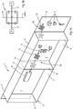
- Fig. 1A is a schematic of an electrical device 1 comprising a housing 3 with walls 5, 6, divided in two compartments 7 by dividing wall 6, each compartment 7 surrounding a filter segment 9 of an electrical high frequency filter, e.g. an LC-filter comprising one or more coils and capacitors.
- the walls 5, 6 of the housing 3 are conductive, e.g. metal or metalized plate material, and form a shield for electromagnetic radiation.
- the housing 3 comprises a circuit board 11, here being provided as a printed circuit board (PCB).
- the housing 3 is mounted onto a top surface of the circuit board 11, wherein the circuit board 11 extends beyond the walls 5, 6 of the housing 3 and the walls 5, 6 being arranged perpendicular to the circuit board 11.
- the circuit board 11 could also be contained fully within the housing and/or one or more of the walls could extend at a non-perpendicular angle to the plane of the circuit board 11.
- (Electrical) components 13 of the device 1 are mounted onto the circuit board 11 and at least some of them are electrically connected by conductive traces 15 on and/or in the circuit board 11.
- walls 5, 6 of the housing 3 extend perpendicular to the circuit board 11.
- One or more compartments 7 may be covered with further wall portions 16, e.g. in the form of a (possibly removable) lid to part of the housing 3 (see Figs. 3A-3B below).
- Signal conductors 17 traverse the shield walls 5 and operably connect the filter segments 9 to each other and a filter segment 9 to at least one further component 13 for transmitting a signal between the filter segments 9 and to the component 13.
- Feedthrough capacitor systems 19 are operably arranged between the signal conductors 17 and the shield walls 5, 6.
- the filter has a plurality of filter segments 9 arranged in series. To prevent unwanted interaction between different filter segments 9, e.g. noise and/or cross talk influences, some of the filter segments 9 are shielded from each other by separation by the dividing shield walls 6 as shown.
- the signal conductor 17 for carrying the signal that is (to be) filtered by the filter segments 9 electrically connects subsequent filter segments 9 and traverses the shield wall 6 for transmitting the signal from one filter segment 9 to the subsequent filter segment 9.
- the feedthrough capacitor system 19 is electrically mounted between the signal conductor and the shield wall, as shown in Fig. 1B .
- Figs. 2A and 2B are schematic cross sections of embodiments of a feedthrough capacitor system 19.
- Figs. 3A and 3B are schematic top views of embodiments of a feedthrough capacitor system 19.
- Figs. 2A , 3A and 3B show the respective feedthrough capacitor system 19 traversing a shield wall 6, the respective feedthrough capacitor systems 19 having the same basic construction.
- Fig. 2A walls 5, 6, 16 are shown to extend on opposite sides of the PCB 11 so that the feedthrough capacitor system 19 and other electrical components (not shown) are surrounded and shielded on both sides of the circuit board 11.
- the circuit board 11 comprises conductive layers 21, 23, 25 and 27 that are electrically insulated from each other, in particular a top (signal) layer 21, a ground layer 23, a middle signal layer 25 and a bottom (ground) layer 27 each carrying conductive traces (see below) and neighbouring layers being separated from each other by insulation layers 29. Note that in other embodiments a circuit board may have less or more layers, and any layers may be differently arranged.
- a plurality of conductive vias 31, 33 are provided through at least part of the circuit board 11 and connect traces on particular layers 21, 23, 25, 27, through one or more intervening layers 23, 25, 27, 29, so that vias 31 connect signal traces 35 on the top layer 21 to signal traces 35 on a signal layer 25 forming signal vias 31, and the vias 33 connect ground traces 37 on the top layer 21 to ground traces 37 on a ground layer 23, 27, forming ground vias 33.
- the shield walls 5, 6 are electrically connected and possibly mechanically connected to ground traces 37, e.g. by soldered connections And/or by conductive elastomers.
- the shield 6 is optionally electrically connected to ground vias 33 for further assuring a common potential for the ground layers and the shield.
- Signal traces 35 and/or ground traces 37 may extend on the respective conductor layers in various shapes and connect various circuit elements, e.g. the shield 6 ( Fig. 3A ) and/or connecting through contact pads 39A, 39B ( Figs. 3A , 3B ).
- Surface mount capacitors 41 are surface mounted onto the traces 35, 37 on the top layer 21.
- the surface mounting comprises electrically and mechanically attaching contacts 43 of the capacitors 41 to the signal and ground traces 35, 37, respectively e.g. by soldering and/or or using a conductive adhesive.
- the terminals 43 of the capacitors 41 are electrically connected to the signal conductor 17 on one side and the shield 6 on the other side with the dielectric portion of the capacitors 41 in between.
- the capacitors 41 on each side of the shield 6 are electrically arranged in parallel to each other, so that their individual capacitances C i add linearly to a combined equivalent capacitance C eq and their inductances L i add reciprocally to a combined equivalent inductance L eq per side.
- a continuous signal conductor 17 is formed by a signal trace 35 on the top layer 21, e.g. starting at contact pad 39A, a signal via 31 into the circuit board 11, a signal trace 35 on signal layer 25 within the circuit board 11 (indicated in broken lines in Fig. 3 ) which traverses the shield 6, another signal via 31 and another signal trace 35 on the top layer 21.
- ground conductors are provided by the ground traces 37 and ground vias 33, wherein the ground conductors are electrically connected to the shield, and in the shown embodiment also being mechanically connected to the latter.
- a ground trace 37 on the top layer 21 of the circuit board 11 overlaps the signal trace 35 within the circuit board 11 and here also is chosen to be wider than that signal trace 35 and in the embodiment of Fig. 3A the ground trace 37 is extended along the shield 6 to serve as a ground connection for the shield 6.
- a similar and possibly substantially identical ground trace may be arranged on a ground layer 27, which layer may also be substantially entirely conductive across a surface occupied by a filter segment 9, a compartment 7, or the entire circuit board 11. Additional ground traces may extend adjacent, and possibly parallel to, the signal trace 35 on a signal layer 25 within the circuit board 11.
- Fig. 2B differs in that the signal conductor 17 extends as wire conductors 45 on opposite sides of the feedthrough capacitor system 19, and not as circuit board traces 35.
- a signal conductor is provided traversing the shield 6 for transmitting a signal from one side of the shield to the opposite side of the shield and being provided with a feedthrough capacitor system 19.
- a feedthrough capacitor system 19 Best seen in Fig. 3 is that in this embodiment the arrangement of the feedthrough capacitors on each side is chosen to be symmetric about the respective signal trace and here also about the respective signal via 31. Further, the arrangements of the capacitors 41 on opposite sides of the shield wall 6 are chosen to be substantially mirror images from each other.
- capacitors need not be positioned as drawn but can be grouped otherwise, also the number of capacitors on both sides of the shield need not be equal in number or size.
Landscapes
- Engineering & Computer Science (AREA)
- Microelectronics & Electronic Packaging (AREA)
- Power Engineering (AREA)
- Manufacturing & Machinery (AREA)
- Health & Medical Sciences (AREA)
- Biomedical Technology (AREA)
- Nuclear Medicine, Radiotherapy & Molecular Imaging (AREA)
- Radiology & Medical Imaging (AREA)
- Life Sciences & Earth Sciences (AREA)
- Animal Behavior & Ethology (AREA)
- General Health & Medical Sciences (AREA)
- Public Health (AREA)
- Veterinary Medicine (AREA)
- Physics & Mathematics (AREA)
- Electromagnetism (AREA)
- Signal Processing (AREA)
- Shielding Devices Or Components To Electric Or Magnetic Fields (AREA)
Claims (15)
- Elektrische Vorrichtung (1), aufweisend ein elektrisches Hochfrequenzfilter (9) und eine Abschirmung (6), die das Filter von mindestens einer weiteren elektrischen Komponente (9, 13) der Vorrichtung separiert, wobei
das Filter (9) konfiguriert ist, ein AC-Signal mit einer Frequenz in einem Bereich von 25 MHz - 30 MHz zu filtern,
die Vorrichtung (1) ferner einen Signalleiter (17) aufweist, der das Filter operativ mit der weiteren Komponente (9, 13) verbindet und die Abschirmung (6) überquert, um das AC-Signal von dem Filter (9) zu der Komponente (9, 13) zu übertragen,
ein Durchführungskondensator-System (19) elektrisch zwischen dem Signalleiter (17) und der Abschirmung (6) angeordnet ist,
wobei das Durchführungskondensator-System (19) mehrere oberflächenmontierte Kondensatoren (41) aufweist, die elektrisch zwischen dem Signalleiter (17) und der Abschirmung (6) angeordnet sind, wobei die oberflächenmontierten Kondensatoren (41) auf einer Leiterplatte (11) oberflächenmontiert sind. - Elektrische Vorrichtung (1) nach Anspruch 1, wobei das Filter (9) ein Filtersegment (9) ist und die weitere elektrische Komponente (9) ein weiteres Filtersegment (9) ist, die Filtersegmente (9) zusammen mindestens einen Teil einer sequentiellen Filtervorrichtung bilden.
- Elektrische Vorrichtung (1) nach einem der vorstehenden Ansprüche, wobei die Abschirmung (6) Teil eines Gehäuses (3) ist, das das Filter (9) mindestens teilweise umgibt und abschirmt.
- Elektrische Vorrichtung (1) nach Anspruch 2 und 3, aufweisend mehrere solcher Gehäuse (3), von denen jedes mindestens ein Filtersegment (9) mindestens teilweise umgibt und abschirmt.
- Elektrische Vorrichtung (1) nach einem der vorstehenden Ansprüche, wobei in dem Durchführungskondensator-System (19) der Signalleiter (17) sich mindestens teilweise an und/oder in der Leiterplatte (11) als eine Signalleiterbahn (25) an und/oder in der Leiterplatte (11) und/oder als eine Signaldurchkontaktierung (31) durch mindestens einen Teil der Leiterplatte (11) erstreckt.
- Elektrische Vorrichtung (1) nach einem der vorstehenden Ansprüche, wobei die Leiterplatte (11) eine Erdungsleiterbahn (37) und/oder eine leitfähige Erdungsdurchkontaktierung (33) aufweist, die elektrisch mit der Abschirmung (6) verbunden ist, wobei die Erdungsleiterbahn (37) Teil einer Erdungsschicht (23, 27) sein kann.
- Elektrische Vorrichtung (1) nach Anspruch 3 und 4, wobei die oberflächenmontierten Kondensatoren (41) an dem Signalleiter (17) und der Erdungsleiterbahn (37) oberflächenmontiert sind.
- Elektrische Vorrichtung (1) nach einem der vorstehenden Ansprüche, wobei eine Vielzahl des einen oder der mehreren oberflächenmontierten Kondensatoren (41) symmetrisch um mindestens einen Teil des Signalabschnitts an der Leiterplatte (11) montiert ist.
- Elektrische Vorrichtung (1) nach einem der vorstehenden Ansprüche, wobei die Schaltkarte mehrere Leiterschichten (21-27) aufweist, der Signalleiter eine Signalleiterbahn (35) an einer Signalschicht (25) in der Leiterplatte (11) aufweist, wobei die Leiterplatte (11) mindestens eine Erdungsleiterbahn (37) und/oder eine Erdungsebene an einer an die Signalschicht (25) angrenzenden Leiterschicht (23, 27) aufweist, wobei die Erdungsleiterbahn (37) und/oder Erdungsebene die Signalleiterbahn (35) überlappt und abschirmt.
- Elektrische Vorrichtung (1) nach einem der vorstehenden Ansprüche, wobei mindestens ein Teil der Abschirmung (6) sich von einer ersten Seite der Schaltkarte in einem im Wesentlichen gestreckten Winkel erstreckt.
- Elektrische Vorrichtung (1) nach einem der vorstehenden Ansprüche, wobei die Vielzahl von oberflächenmontierten Kondensatoren (41) eine erste Vielzahl von oberflächenmontierten Kondensatoren (41) und eine zweite Vielzahl von oberflächenmontierten Kondensatoren (41) aufweist, die an sich gegenüberliegenden Seiten der Abschirmung (6) an der Leiterplatte (11) angeordnet sind.
- Elektrische Vorrichtung (1) nach Anspruch 11, wobei die erste und zweite Vielzahl von oberflächenmontierten Kondensatoren (41) bereitgestellt sind als gegenseitige Spiegelbilder in Bezug auf Kapazitäten und Positionen der einzelnen Kondensatoren (41) relativ zu der Abschirmung (6) und/oder bezüglich einer Haupterstreckungsrichtung des Signalleiters (35) zwischen der ersten und zweiten Vielzahl von oberflächenmontierten Kondensatoren (41).
- Elektrische Vorrichtung (1) nach einem der vorstehenden Ansprüche, wobei das Filter (9) konfiguriert ist, um das AC-Signal mit einer Leistung in einem Bereich von 2 - 2000 W zu filtern.
- Physiotherapie-Vorrichtung aufweisend die elektrische Vorrichtung (1) nach einem der vorstehenden Ansprüche.
- Physiotherapie-Vorrichtung nach Anspruch 14, die für eine Behandlung eines Individuums mit kontinuierlicher und/oder gepulster Kurzwellen-Elektrotherapie konfiguriert ist, wobei das Filter (9) konfiguriert ist, eine Frequenz von 26-28 MHz, mit 250-350 Volt Spitzezu-Spitze und 150-250 W erzeugter Leistung zu filtern.
Applications Claiming Priority (2)
| Application Number | Priority Date | Filing Date | Title |
|---|---|---|---|
| EP17166094 | 2017-04-11 | ||
| PCT/EP2018/059256 WO2018189226A1 (en) | 2017-04-11 | 2018-04-11 | Electrical device comprising filter and feedthrough capacitor |
Publications (2)
| Publication Number | Publication Date |
|---|---|
| EP3610709A1 EP3610709A1 (de) | 2020-02-19 |
| EP3610709B1 true EP3610709B1 (de) | 2021-06-09 |
Family
ID=58714886
Family Applications (1)
| Application Number | Title | Priority Date | Filing Date |
|---|---|---|---|
| EP18715740.9A Active EP3610709B1 (de) | 2017-04-11 | 2018-04-11 | Elektrische vorrichtung mit filter und mit durchführungskondensator |
Country Status (4)
| Country | Link |
|---|---|
| US (1) | US11564339B2 (de) |
| EP (1) | EP3610709B1 (de) |
| CA (1) | CA3058693C (de) |
| WO (1) | WO2018189226A1 (de) |
Families Citing this family (2)
| Publication number | Priority date | Publication date | Assignee | Title |
|---|---|---|---|---|
| EP3700005A1 (de) * | 2019-02-25 | 2020-08-26 | Nokia Solutions and Networks Oy | Senden und/oder empfangen von hochfrequenzsignalen |
| CN111953205A (zh) * | 2020-07-23 | 2020-11-17 | 重庆大及电子科技有限公司 | 大功率滤波保护装置及框架式滤波结构 |
Family Cites Families (25)
| Publication number | Priority date | Publication date | Assignee | Title |
|---|---|---|---|---|
| US5285007A (en) * | 1992-02-03 | 1994-02-08 | Digital Equipment Corporation | System for reducing the emission of high frequency electromagnetic waves from computer systems |
| JPH06268464A (ja) * | 1993-03-17 | 1994-09-22 | Mitsubishi Materials Corp | ノイズフィルタブロック |
| US5590029A (en) * | 1995-01-12 | 1996-12-31 | Dell Usa, L.P. | Circuit board SMT device mounting apparatus |
| US5895980A (en) * | 1996-12-30 | 1999-04-20 | Medical Pacing Concepts, Ltd. | Shielded pacemaker enclosure |
| US5830016A (en) * | 1997-01-29 | 1998-11-03 | Chuang; Johnson | Interference-proof device for electric connector |
| US5896267A (en) * | 1997-07-10 | 1999-04-20 | Greatbatch-Hittman, Inc. | Substrate mounted filter for feedthrough devices |
| US5959829A (en) * | 1998-02-18 | 1999-09-28 | Maxwell Energy Products, Inc. | Chip capacitor electromagnetic interference filter |
| US5973906A (en) * | 1998-03-17 | 1999-10-26 | Maxwell Energy Products, Inc. | Chip capacitors and chip capacitor electromagnetic interference filters |
| US6424234B1 (en) * | 1998-09-18 | 2002-07-23 | Greatbatch-Sierra, Inc. | Electromagnetic interference (emi) filter and process for providing electromagnetic compatibility of an electronic device while in the presence of an electromagnetic emitter operating at the same frequency |
| US6377845B1 (en) * | 2000-07-25 | 2002-04-23 | Datascope Investment Corp. | Method and device for sensing impedance respiration |
| US6473314B1 (en) | 2000-08-03 | 2002-10-29 | Powerwave Technologies, Inc. | RF power amplifier assembly employing multi-layer RF blocking filter |
| US6900383B2 (en) * | 2001-03-19 | 2005-05-31 | Hewlett-Packard Development Company, L.P. | Board-level EMI shield that adheres to and conforms with printed circuit board component and board surfaces |
| CA2482202C (en) * | 2001-04-13 | 2012-07-03 | Surgi-Vision, Inc. | Systems and methods for magnetic-resonance-guided interventional procedures |
| KR100432361B1 (ko) * | 2001-05-29 | 2004-05-22 | 김성열 | 차폐기능 및 장착기능을 개선한 관통형 필터 |
| US7295086B2 (en) * | 2002-10-23 | 2007-11-13 | Spectrum Control Inc. | Dielectric component array with failsafe link |
| JP2004207419A (ja) | 2002-12-25 | 2004-07-22 | Toshiba Corp | 貫通コンデンサ装置 |
| JP2004327690A (ja) * | 2003-04-24 | 2004-11-18 | Fuji Xerox Co Ltd | プリント配線基板 |
| JP4258309B2 (ja) | 2003-08-01 | 2009-04-30 | 住友電気工業株式会社 | 半導体製造装置用サセプタおよびそれを搭載した半導体製造装置 |
| US20070123949A1 (en) * | 2005-11-11 | 2007-05-31 | Greatbatch Ltd. | Low loss band pass filter for rf distance telemetry pin antennas of active implantable medical devices |
| US9042999B2 (en) * | 2006-06-08 | 2015-05-26 | Greatbatch Ltd. | Low loss band pass filter for RF distance telemetry pin antennas of active implantable medical devices |
| US9463329B2 (en) * | 2008-03-20 | 2016-10-11 | Greatbatch Ltd. | Shielded three-terminal flat-through EMI/energy dissipating filter with co-fired hermetically sealed feedthrough |
| CN201490970U (zh) | 2009-08-19 | 2010-05-26 | 中兴通讯股份有限公司 | 一种功放结构 |
| CN104735908A (zh) * | 2013-12-18 | 2015-06-24 | 深圳富泰宏精密工业有限公司 | 印刷电路板 |
| EP3552661A1 (de) * | 2014-02-21 | 2019-10-16 | Cardiac Pacemakers, Inc. | Gefilterte durchführungsanordnung für implantierbare medizinische elektronische vorrichtungen |
| CN107405496B (zh) * | 2015-03-31 | 2021-01-08 | 心脏起搏器股份公司 | 用于可植入医疗装置的封装式滤波馈通 |
-
2018
- 2018-04-11 EP EP18715740.9A patent/EP3610709B1/de active Active
- 2018-04-11 CA CA3058693A patent/CA3058693C/en active Active
- 2018-04-11 WO PCT/EP2018/059256 patent/WO2018189226A1/en not_active Ceased
- 2018-04-11 US US16/603,758 patent/US11564339B2/en active Active
Non-Patent Citations (1)
| Title |
|---|
| None * |
Also Published As
| Publication number | Publication date |
|---|---|
| US11564339B2 (en) | 2023-01-24 |
| EP3610709A1 (de) | 2020-02-19 |
| WO2018189226A1 (en) | 2018-10-18 |
| CA3058693A1 (en) | 2018-10-18 |
| CA3058693C (en) | 2023-08-22 |
| US20200137932A1 (en) | 2020-04-30 |
Similar Documents
| Publication | Publication Date | Title |
|---|---|---|
| JP3225181U (ja) | プラグコネクタ及び構成要素 | |
| US5111169A (en) | Lc noise filter | |
| KR100367859B1 (ko) | 적층 커패시터와 감결합 커패시터의 배선접속구조, 및배선기판 | |
| KR100564928B1 (ko) | 전송선로형 컴포넌트 | |
| US8354975B2 (en) | Electromagnetic band gap element, and antenna and filter using the same | |
| US20110278947A1 (en) | Antenna device, transponder reader, induction cooker | |
| US20200036086A1 (en) | Electronic device and communication apparatus | |
| EP3610709B1 (de) | Elektrische vorrichtung mit filter und mit durchführungskondensator | |
| US10154616B2 (en) | Electromagnetic interference filter for implanted electronics | |
| JP5686090B2 (ja) | ノイズフィルタが搭載された電子装置 | |
| JP2013539218A (ja) | 高周波に使用するための多平面印刷配線板 | |
| EP2544368B1 (de) | Oberflächenmontierbarer Mehrschicht-Keramikfilter | |
| US20250037931A1 (en) | Choke module | |
| JP6202112B2 (ja) | ノイズ低減用電子部品 | |
| Liotta et al. | A novel capacitive-inductive channel for wireless power and data transmission | |
| US9460885B2 (en) | Magnetron filter | |
| JPH09232014A (ja) | インタフェースケーブル接続用コネクタ | |
| JP7403854B2 (ja) | 磁気共鳴環境用の神経モニタリングケーブル | |
| US12388359B2 (en) | Power conversion device | |
| CN106374867A (zh) | 陷波器及配置有陷波器的磁共振成像装置 | |
| JPH09246776A (ja) | プリント配線板 | |
| CN102545220A (zh) | 一种用于低泄漏电流的屏蔽方舱电源、信号组合式滤波器及其设计方法 | |
| JP4338040B2 (ja) | 高電圧コンデンサ、高電圧コンデンサ装置、及び、マグネトロン | |
| HK40063665A (en) | Neurological monitoring cable for magnetic resonance environments | |
| JPH11195384A (ja) | マグネトロン用の付加的な回路装置 |
Legal Events
| Date | Code | Title | Description |
|---|---|---|---|
| STAA | Information on the status of an ep patent application or granted ep patent |
Free format text: STATUS: UNKNOWN |
|
| STAA | Information on the status of an ep patent application or granted ep patent |
Free format text: STATUS: THE INTERNATIONAL PUBLICATION HAS BEEN MADE |
|
| PUAI | Public reference made under article 153(3) epc to a published international application that has entered the european phase |
Free format text: ORIGINAL CODE: 0009012 |
|
| STAA | Information on the status of an ep patent application or granted ep patent |
Free format text: STATUS: REQUEST FOR EXAMINATION WAS MADE |
|
| 17P | Request for examination filed |
Effective date: 20191018 |
|
| AK | Designated contracting states |
Kind code of ref document: A1 Designated state(s): AL AT BE BG CH CY CZ DE DK EE ES FI FR GB GR HR HU IE IS IT LI LT LU LV MC MK MT NL NO PL PT RO RS SE SI SK SM TR |
|
| AX | Request for extension of the european patent |
Extension state: BA ME |
|
| DAV | Request for validation of the european patent (deleted) | ||
| DAX | Request for extension of the european patent (deleted) | ||
| GRAP | Despatch of communication of intention to grant a patent |
Free format text: ORIGINAL CODE: EPIDOSNIGR1 |
|
| STAA | Information on the status of an ep patent application or granted ep patent |
Free format text: STATUS: GRANT OF PATENT IS INTENDED |
|
| INTG | Intention to grant announced |
Effective date: 20201215 |
|
| GRAS | Grant fee paid |
Free format text: ORIGINAL CODE: EPIDOSNIGR3 |
|
| GRAA | (expected) grant |
Free format text: ORIGINAL CODE: 0009210 |
|
| STAA | Information on the status of an ep patent application or granted ep patent |
Free format text: STATUS: THE PATENT HAS BEEN GRANTED |
|
| AK | Designated contracting states |
Kind code of ref document: B1 Designated state(s): AL AT BE BG CH CY CZ DE DK EE ES FI FR GB GR HR HU IE IS IT LI LT LU LV MC MK MT NL NO PL PT RO RS SE SI SK SM TR |
|
| REG | Reference to a national code |
Ref country code: GB Ref legal event code: FG4D |
|
| REG | Reference to a national code |
Ref country code: CH Ref legal event code: EP Ref country code: AT Ref legal event code: REF Ref document number: 1401537 Country of ref document: AT Kind code of ref document: T Effective date: 20210615 |
|
| REG | Reference to a national code |
Ref country code: DE Ref legal event code: R096 Ref document number: 602018018361 Country of ref document: DE |
|
| REG | Reference to a national code |
Ref country code: IE Ref legal event code: FG4D |
|
| REG | Reference to a national code |
Ref country code: LT Ref legal event code: MG9D |
|
| PG25 | Lapsed in a contracting state [announced via postgrant information from national office to epo] |
Ref country code: FI Free format text: LAPSE BECAUSE OF FAILURE TO SUBMIT A TRANSLATION OF THE DESCRIPTION OR TO PAY THE FEE WITHIN THE PRESCRIBED TIME-LIMIT Effective date: 20210609 Ref country code: LT Free format text: LAPSE BECAUSE OF FAILURE TO SUBMIT A TRANSLATION OF THE DESCRIPTION OR TO PAY THE FEE WITHIN THE PRESCRIBED TIME-LIMIT Effective date: 20210609 Ref country code: HR Free format text: LAPSE BECAUSE OF FAILURE TO SUBMIT A TRANSLATION OF THE DESCRIPTION OR TO PAY THE FEE WITHIN THE PRESCRIBED TIME-LIMIT Effective date: 20210609 Ref country code: BG Free format text: LAPSE BECAUSE OF FAILURE TO SUBMIT A TRANSLATION OF THE DESCRIPTION OR TO PAY THE FEE WITHIN THE PRESCRIBED TIME-LIMIT Effective date: 20210909 |
|
| REG | Reference to a national code |
Ref country code: AT Ref legal event code: MK05 Ref document number: 1401537 Country of ref document: AT Kind code of ref document: T Effective date: 20210609 |
|
| REG | Reference to a national code |
Ref country code: NL Ref legal event code: MP Effective date: 20210609 |
|
| PG25 | Lapsed in a contracting state [announced via postgrant information from national office to epo] |
Ref country code: GR Free format text: LAPSE BECAUSE OF FAILURE TO SUBMIT A TRANSLATION OF THE DESCRIPTION OR TO PAY THE FEE WITHIN THE PRESCRIBED TIME-LIMIT Effective date: 20210910 Ref country code: RS Free format text: LAPSE BECAUSE OF FAILURE TO SUBMIT A TRANSLATION OF THE DESCRIPTION OR TO PAY THE FEE WITHIN THE PRESCRIBED TIME-LIMIT Effective date: 20210609 Ref country code: SE Free format text: LAPSE BECAUSE OF FAILURE TO SUBMIT A TRANSLATION OF THE DESCRIPTION OR TO PAY THE FEE WITHIN THE PRESCRIBED TIME-LIMIT Effective date: 20210609 Ref country code: LV Free format text: LAPSE BECAUSE OF FAILURE TO SUBMIT A TRANSLATION OF THE DESCRIPTION OR TO PAY THE FEE WITHIN THE PRESCRIBED TIME-LIMIT Effective date: 20210609 Ref country code: NO Free format text: LAPSE BECAUSE OF FAILURE TO SUBMIT A TRANSLATION OF THE DESCRIPTION OR TO PAY THE FEE WITHIN THE PRESCRIBED TIME-LIMIT Effective date: 20210909 |
|
| PG25 | Lapsed in a contracting state [announced via postgrant information from national office to epo] |
Ref country code: NL Free format text: LAPSE BECAUSE OF FAILURE TO SUBMIT A TRANSLATION OF THE DESCRIPTION OR TO PAY THE FEE WITHIN THE PRESCRIBED TIME-LIMIT Effective date: 20210609 Ref country code: RO Free format text: LAPSE BECAUSE OF FAILURE TO SUBMIT A TRANSLATION OF THE DESCRIPTION OR TO PAY THE FEE WITHIN THE PRESCRIBED TIME-LIMIT Effective date: 20210609 Ref country code: PT Free format text: LAPSE BECAUSE OF FAILURE TO SUBMIT A TRANSLATION OF THE DESCRIPTION OR TO PAY THE FEE WITHIN THE PRESCRIBED TIME-LIMIT Effective date: 20211011 Ref country code: CZ Free format text: LAPSE BECAUSE OF FAILURE TO SUBMIT A TRANSLATION OF THE DESCRIPTION OR TO PAY THE FEE WITHIN THE PRESCRIBED TIME-LIMIT Effective date: 20210609 Ref country code: AT Free format text: LAPSE BECAUSE OF FAILURE TO SUBMIT A TRANSLATION OF THE DESCRIPTION OR TO PAY THE FEE WITHIN THE PRESCRIBED TIME-LIMIT Effective date: 20210609 Ref country code: ES Free format text: LAPSE BECAUSE OF FAILURE TO SUBMIT A TRANSLATION OF THE DESCRIPTION OR TO PAY THE FEE WITHIN THE PRESCRIBED TIME-LIMIT Effective date: 20210609 Ref country code: EE Free format text: LAPSE BECAUSE OF FAILURE TO SUBMIT A TRANSLATION OF THE DESCRIPTION OR TO PAY THE FEE WITHIN THE PRESCRIBED TIME-LIMIT Effective date: 20210609 Ref country code: SK Free format text: LAPSE BECAUSE OF FAILURE TO SUBMIT A TRANSLATION OF THE DESCRIPTION OR TO PAY THE FEE WITHIN THE PRESCRIBED TIME-LIMIT Effective date: 20210609 Ref country code: SM Free format text: LAPSE BECAUSE OF FAILURE TO SUBMIT A TRANSLATION OF THE DESCRIPTION OR TO PAY THE FEE WITHIN THE PRESCRIBED TIME-LIMIT Effective date: 20210609 |
|
| PG25 | Lapsed in a contracting state [announced via postgrant information from national office to epo] |
Ref country code: PL Free format text: LAPSE BECAUSE OF FAILURE TO SUBMIT A TRANSLATION OF THE DESCRIPTION OR TO PAY THE FEE WITHIN THE PRESCRIBED TIME-LIMIT Effective date: 20210609 |
|
| REG | Reference to a national code |
Ref country code: DE Ref legal event code: R097 Ref document number: 602018018361 Country of ref document: DE |
|
| PLBE | No opposition filed within time limit |
Free format text: ORIGINAL CODE: 0009261 |
|
| STAA | Information on the status of an ep patent application or granted ep patent |
Free format text: STATUS: NO OPPOSITION FILED WITHIN TIME LIMIT |
|
| PG25 | Lapsed in a contracting state [announced via postgrant information from national office to epo] |
Ref country code: DK Free format text: LAPSE BECAUSE OF FAILURE TO SUBMIT A TRANSLATION OF THE DESCRIPTION OR TO PAY THE FEE WITHIN THE PRESCRIBED TIME-LIMIT Effective date: 20210609 |
|
| 26N | No opposition filed |
Effective date: 20220310 |
|
| PG25 | Lapsed in a contracting state [announced via postgrant information from national office to epo] |
Ref country code: AL Free format text: LAPSE BECAUSE OF FAILURE TO SUBMIT A TRANSLATION OF THE DESCRIPTION OR TO PAY THE FEE WITHIN THE PRESCRIBED TIME-LIMIT Effective date: 20210609 |
|
| REG | Reference to a national code |
Ref country code: CH Ref legal event code: PL |
|
| PG25 | Lapsed in a contracting state [announced via postgrant information from national office to epo] |
Ref country code: MC Free format text: LAPSE BECAUSE OF FAILURE TO SUBMIT A TRANSLATION OF THE DESCRIPTION OR TO PAY THE FEE WITHIN THE PRESCRIBED TIME-LIMIT Effective date: 20210609 Ref country code: LU Free format text: LAPSE BECAUSE OF NON-PAYMENT OF DUE FEES Effective date: 20220411 Ref country code: LI Free format text: LAPSE BECAUSE OF NON-PAYMENT OF DUE FEES Effective date: 20220430 Ref country code: FR Free format text: LAPSE BECAUSE OF NON-PAYMENT OF DUE FEES Effective date: 20220430 Ref country code: CH Free format text: LAPSE BECAUSE OF NON-PAYMENT OF DUE FEES Effective date: 20220430 |
|
| PG25 | Lapsed in a contracting state [announced via postgrant information from national office to epo] |
Ref country code: IE Free format text: LAPSE BECAUSE OF NON-PAYMENT OF DUE FEES Effective date: 20220411 |
|
| PG25 | Lapsed in a contracting state [announced via postgrant information from national office to epo] |
Ref country code: MK Free format text: LAPSE BECAUSE OF FAILURE TO SUBMIT A TRANSLATION OF THE DESCRIPTION OR TO PAY THE FEE WITHIN THE PRESCRIBED TIME-LIMIT Effective date: 20210609 Ref country code: CY Free format text: LAPSE BECAUSE OF FAILURE TO SUBMIT A TRANSLATION OF THE DESCRIPTION OR TO PAY THE FEE WITHIN THE PRESCRIBED TIME-LIMIT Effective date: 20210609 |
|
| PG25 | Lapsed in a contracting state [announced via postgrant information from national office to epo] |
Ref country code: HU Free format text: LAPSE BECAUSE OF FAILURE TO SUBMIT A TRANSLATION OF THE DESCRIPTION OR TO PAY THE FEE WITHIN THE PRESCRIBED TIME-LIMIT; INVALID AB INITIO Effective date: 20180411 |
|
| PG25 | Lapsed in a contracting state [announced via postgrant information from national office to epo] |
Ref country code: TR Free format text: LAPSE BECAUSE OF FAILURE TO SUBMIT A TRANSLATION OF THE DESCRIPTION OR TO PAY THE FEE WITHIN THE PRESCRIBED TIME-LIMIT Effective date: 20210609 |
|
| PG25 | Lapsed in a contracting state [announced via postgrant information from national office to epo] |
Ref country code: MT Free format text: LAPSE BECAUSE OF FAILURE TO SUBMIT A TRANSLATION OF THE DESCRIPTION OR TO PAY THE FEE WITHIN THE PRESCRIBED TIME-LIMIT Effective date: 20210609 |
|
| PGFP | Annual fee paid to national office [announced via postgrant information from national office to epo] |
Ref country code: DE Payment date: 20250429 Year of fee payment: 8 |
|
| PGFP | Annual fee paid to national office [announced via postgrant information from national office to epo] |
Ref country code: GB Payment date: 20250428 Year of fee payment: 8 |
|
| PGFP | Annual fee paid to national office [announced via postgrant information from national office to epo] |
Ref country code: BE Payment date: 20250428 Year of fee payment: 8 Ref country code: IT Payment date: 20250422 Year of fee payment: 8 |