EP3611559B1 - Flüssigkristalllichtanpassungsvorrichtung und flüssigkristalllichtanpassungsverfahren - Google Patents
Flüssigkristalllichtanpassungsvorrichtung und flüssigkristalllichtanpassungsverfahren Download PDFInfo
- Publication number
- EP3611559B1 EP3611559B1 EP18783764.6A EP18783764A EP3611559B1 EP 3611559 B1 EP3611559 B1 EP 3611559B1 EP 18783764 A EP18783764 A EP 18783764A EP 3611559 B1 EP3611559 B1 EP 3611559B1
- Authority
- EP
- European Patent Office
- Prior art keywords
- voltage
- power supply
- liquid crystal
- supply voltage
- comparator
- Prior art date
- Legal status (The legal status is an assumption and is not a legal conclusion. Google has not performed a legal analysis and makes no representation as to the accuracy of the status listed.)
- Active
Links
Images





Classifications
-
- G—PHYSICS
- G09—EDUCATION; CRYPTOGRAPHY; DISPLAY; ADVERTISING; SEALS
- G09G—ARRANGEMENTS OR CIRCUITS FOR CONTROL OF INDICATING DEVICES USING STATIC MEANS TO PRESENT VARIABLE INFORMATION
- G09G3/00—Control arrangements or circuits, of interest only in connection with visual indicators other than cathode-ray tubes
- G09G3/20—Control arrangements or circuits, of interest only in connection with visual indicators other than cathode-ray tubes for presentation of an assembly of a number of characters, e.g. a page, by composing the assembly by combination of individual elements arranged in a matrix no fixed position being assigned to or needed to be assigned to the individual characters or partial characters
- G09G3/34—Control arrangements or circuits, of interest only in connection with visual indicators other than cathode-ray tubes for presentation of an assembly of a number of characters, e.g. a page, by composing the assembly by combination of individual elements arranged in a matrix no fixed position being assigned to or needed to be assigned to the individual characters or partial characters by control of light from an independent source
- G09G3/36—Control arrangements or circuits, of interest only in connection with visual indicators other than cathode-ray tubes for presentation of an assembly of a number of characters, e.g. a page, by composing the assembly by combination of individual elements arranged in a matrix no fixed position being assigned to or needed to be assigned to the individual characters or partial characters by control of light from an independent source using liquid crystals
- G09G3/3611—Control of matrices with row and column drivers
- G09G3/3696—Generation of voltages supplied to electrode drivers
-
- G—PHYSICS
- G02—OPTICS
- G02F—OPTICAL DEVICES OR ARRANGEMENTS FOR THE CONTROL OF LIGHT BY MODIFICATION OF THE OPTICAL PROPERTIES OF THE MEDIA OF THE ELEMENTS INVOLVED THEREIN; NON-LINEAR OPTICS; FREQUENCY-CHANGING OF LIGHT; OPTICAL LOGIC ELEMENTS; OPTICAL ANALOGUE/DIGITAL CONVERTERS
- G02F1/00—Devices or arrangements for the control of the intensity, colour, phase, polarisation or direction of light arriving from an independent light source, e.g. switching, gating or modulating; Non-linear optics
- G02F1/01—Devices or arrangements for the control of the intensity, colour, phase, polarisation or direction of light arriving from an independent light source, e.g. switching, gating or modulating; Non-linear optics for the control of the intensity, phase, polarisation or colour
- G02F1/13—Devices or arrangements for the control of the intensity, colour, phase, polarisation or direction of light arriving from an independent light source, e.g. switching, gating or modulating; Non-linear optics for the control of the intensity, phase, polarisation or colour based on liquid crystals, e.g. single liquid crystal display cells
- G02F1/133—Constructional arrangements; Operation of liquid crystal cells; Circuit arrangements
- G02F1/13306—Circuit arrangements or driving methods for the control of single liquid crystal cells
-
- G—PHYSICS
- G02—OPTICS
- G02F—OPTICAL DEVICES OR ARRANGEMENTS FOR THE CONTROL OF LIGHT BY MODIFICATION OF THE OPTICAL PROPERTIES OF THE MEDIA OF THE ELEMENTS INVOLVED THEREIN; NON-LINEAR OPTICS; FREQUENCY-CHANGING OF LIGHT; OPTICAL LOGIC ELEMENTS; OPTICAL ANALOGUE/DIGITAL CONVERTERS
- G02F1/00—Devices or arrangements for the control of the intensity, colour, phase, polarisation or direction of light arriving from an independent light source, e.g. switching, gating or modulating; Non-linear optics
- G02F1/01—Devices or arrangements for the control of the intensity, colour, phase, polarisation or direction of light arriving from an independent light source, e.g. switching, gating or modulating; Non-linear optics for the control of the intensity, phase, polarisation or colour
- G02F1/13—Devices or arrangements for the control of the intensity, colour, phase, polarisation or direction of light arriving from an independent light source, e.g. switching, gating or modulating; Non-linear optics for the control of the intensity, phase, polarisation or colour based on liquid crystals, e.g. single liquid crystal display cells
- G02F1/133—Constructional arrangements; Operation of liquid crystal cells; Circuit arrangements
- G02F1/1333—Constructional arrangements; Manufacturing methods
- G02F1/1334—Constructional arrangements; Manufacturing methods based on polymer dispersed liquid crystals, e.g. microencapsulated liquid crystals
-
- G—PHYSICS
- G09—EDUCATION; CRYPTOGRAPHY; DISPLAY; ADVERTISING; SEALS
- G09G—ARRANGEMENTS OR CIRCUITS FOR CONTROL OF INDICATING DEVICES USING STATIC MEANS TO PRESENT VARIABLE INFORMATION
- G09G2330/00—Aspects of power supply; Aspects of display protection and defect management
- G09G2330/02—Details of power systems and of start or stop of display operation
- G09G2330/021—Power management, e.g. power saving
Definitions
- the present invention relates generally to a liquid crystal optical modulation device and a liquid crystal optical modulation method suitable for light control glass using a polymer dispersed-type liquid crystal in particular.
- Patent Literature 1 discloses a modulator for dimming the AC voltage of an AC power source that is supplied to an LCD device.
- Patent Literature 1 Jpn. Pat. Appln. KOKAI Publication No. 2013-072895
- FIGS. 8A and 8B illustrate a general configuration in which a polymer dispersed-type liquid crystal panel is applied to a light control glass 10 having a simple blind function.
- FIG. 8A shows the power off state.
- the polymer dispersed liquid crystal 17 is sealed and filled in an inside defined by transparent electrodes 13 and 14 on inner surface sides of two parallel plate glasses 11 and 12 as substrates, and spacers 15 and 16.
- a commercial power source 18 and a switch 19 are connected to the transparent electrodes 13 and 14.
- the switch 19 is off, no voltage from the commercial power source 18 is applied to the polymer dispersed liquid crystal 17 between the transparent electrodes 13 and 14.
- the polymer dispersed liquid crystal 17 as shown in the figure, a large number of liquid crystal molecules along mesh-like polymer fibers inside are irregularly arranged, so that light cannot be transmitted through the two glass plates 11 and 12 and is scattered. Since the light control glass 10 of this state scatters light as in the case of frosted glass and cannot transmit most of the light, the whole glass becomes white when seen from the indoor side. Therefore, for example, even if a tree is present outside the light control glass 10, a silhouette of the tree will appear only vaguely.
- FIG. 8B shows a state in which the switch 19 is turned on.
- a voltage is applied to the polymer dispersed liquid crystal 17 between the transparent electrodes 13 and 14 to form an electric field, and liquid crystal molecules in the polymer dispersed liquid crystal 17 are aligned with their major axes in the direction orthogonal to the glass surface. Accordingly, the two glass plates 11 and 12 transmit the light and become transparent.
- the whole of the light control glass 10 in this state looks transparent when seen from the indoor side, and a tree present outside the light control glass 10 is clearly visible.
- FIGS. 8A and 8B show how the light control glass 10 looks in the off state and the on state; however, in this type of light control glass 10, it is possible to perform halftone driving, thereby performing light control driving for steplessly adjusting a semitransparent condition between the scattering and the transmission.
- FIG. 9 exemplifies a voltage waveform of AC 100 [V] which is a general commercial power source used in homes and companies.
- This figure shows the same voltage waveform of frequency 60 [Hz] at an effective voltage 100 [V]; when the effective voltage is 100 [V], the peak value is approximately 141 [V].
- the peak value greatly exceeds the general withstand voltage of the liquid crystal element used as the light control glass 10, and the power supply voltage cannot be directly applied as the drive voltage.
- the light control glass 10 it is necessary to provide a terminal portion connected to both of the transparent electrodes 13 and 14 at one end of the flat structure, generally near a corner portion, due to the installation structure in a house, etc. Therefore, a voltage drop occurs because of resistance and capacitance of the light control glass as an optical modulation element.
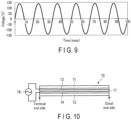
- FIG. 10 shows a state in which the light control glass 10 is connected to the commercial power source 18 at the left end side as a terminal side, while the right end in FIG. 10 is a distal end side. Therefore, depending on the size of the light control glass 10, even if a voltage at the maximum value according to the withstand voltage standard is applied from the commercial power source 18 to the terminal side, the voltage cannot reach the threshold of the voltage for driving the liquid crystal constituting the light control glass 10 at the distal end portion opposite to the terminal portion. As a result, there is a possibility that the entire surface cannot be uniformly shifted to the transmission mode.
- FIG. 11 is a simplified diagram showing a configuration of an equivalent circuit electrically representing the light control glass 10. As shown in the figure, resistors R1 to R22 and capacitors C1 to C4 are arranged and connected in a ladder shape, between the terminal side at the left end and the distal end side at the right end.
- FIG. 12 shows respective waveforms of a terminal side voltage TV and a distal end side voltage EV when sine wave AC power supply having a peak voltage value of 70 [V] (effective voltage value of about 50 [V]) is applied to the light control glass 10.
- the distal end side voltage EV has a peak value lower than that of the terminal side voltage TV, so that the peak voltage value is about 35 [V] (the effective voltage value is about 25 [V]).
- the present invention has been made in view of the above situation. It is an object of the present invention to provide a liquid crystal optical modulation device and a liquid crystal optical modulation method that can realize uniform optical modulation control without causing surface unevenness and the like, while driving with lower power consumption.
- a liquid crystal optical modulation device according to claim 1.
- the present invention it is possible to realize uniform optical modulation control without causing surface unevenness and the like, while driving with lower power consumption.
- FIG. 1 is a block diagram showing a circuit configuration of a liquid crystal optical modulation device 20 according to an embodiment of the present invention.
- a numeral 21 denotes a commercial power source of AC 100 [V], one end thereof is grounded, and the power supply voltage from the other end is applied to an optical modulation element 29 through switching circuits 27 and 28.
- the switching circuits 27 and 28 corresponds to a voltage limiting section for limiting the power supply voltage from the commercial AC source 21 applied to the liquid crystal panel, which is the optical modulation element 29. Further, the liquid crystal optical modulation device 20 is provided with a control system (control section) including a comparator portion 22 which controls the voltage applied to an optical modulation element 29 by the switching circuits 27 and 28 according to the phase of the power supply voltage of the commercial AC source 21, a zero-cross comparator portion 23, a timing generation circuit 24, and gate drivers 25 and 26.
- control system control section
- the optical modulation element 29 indicates a light control glass, which is a drive control target of the liquid crystal optical modulation device 20, and has an equivalent circuit configuration as shown in FIG. 11 above.
- the optical modulation element 29 is represented as a resistor RL9 and a capacitance CL 9 connected in series. The other end side of the capacitance CL9 that is not connected to the resistor RL9 is grounded.
- the switching circuit 27 includes an N-channel MOSFET 27a and its parasitic diode (D+) 27b, and applies the AC power supply from the commercial power source 21 to a drain of the MOSFET 27a and a cathode of the parasitic diode 27b.
- the switching circuit 28 includes an N-channel MOSFET 28a and its parasitic diode (D-) 28b, and a source of the MOSFET 27a of the switching circuit 27 and an anode of the parasitic diode 27b are connected to a source of the MOSFET 28a and an anode of the parasitic diode 28b.
- a drain of the MOSFET 28a and a cathode of the parasitic diode 28b are connected to one end of the resistor RL9 of the optical modulation element 29.
- switching circuits 27 and 28 are constituted by using bipolar transistors instead of the MOSFETs, equivalent functions can be realized by connecting external diodes for rectification in addition.
- a resistance voltage dividing portion is formed of resistors R31 and R32, and the AC power supply from the commercial power source 21 is applied to one end of the resistor R31. The other end of the resistor R32 that is not connected to the resistor R31 is grounded.
- the resistors R31 and R32 divide the commercial power source voltage from the commercial power source 21 into 1/20 with resistance values of, for example, 190 [kQ] and 10 [kQ].
- the commercial power source voltage from the commercial power source 21 has an effective value of 100 [V], that is, the peak value is ⁇ 141 [V]
- the potential at the connection middle point between the resistor R31 and the resistor R32 changes within a range of ⁇ 7.05 [V].
- the potential at the connection middle point is supplied to each of plus (+) inputs of comparators 22a and 22b and a minus (-) input of a comparator 22c of the comparator portion 22, and a plus (+) input of a comparator 23a of the zero-cross comparator portion 23.
- a resistor R33 and a resistor R34 constituting a resistance voltage dividing portion having a voltage dividing ratio equal to that of the resistance voltage dividing portion constituted by the resistor R31 and the resistor R32 are provided, and the potential between the switching circuit 28 and the optical modulation element 29 is applied to one end of the resistor R33.
- the other end of the resistor R34 that is not connected to the resistor R33 is grounded.
- the resistors R33 and R34 also divide the voltage supplied to the optical modulation element 29 into 1/20 with resistance values of, for example, 190 [kQ] and 10 [kQ], and the potential at the connection middle point is supplied to a minus (-) input of the comparator 22a that constitutes the comparator 22.
- the DC voltage value from a variable DC power supply 22d is given to the minus (-) input to the comparator 22b of the comparator 22.
- the variable DC power supply 22d generates, as a reference voltage corresponding to the voltage +Vc, a discretionary voltage within a range of 0 [V] to +3.5 [V], which is 1/20 of a positive withstand voltage limit of +70 [V] as the maximum value, in accordance with the voltage division ratio of the resistors R31 and R32, and applies the generated reference voltage to the minus (-) input of the comparator 22b.
- the DC voltage value from a variable DC power supply 22e is given to the plus (+) input to the comparator 22c of the comparator 22.
- the variable DC power supply 22e generates, as a reference voltage corresponding to the voltage -Vc, a discretionary voltage within a range of 0 [V] to -3.5 [V], which is 1/20 of a negative withstand voltage limit of -70 [V] as the minimum value, in accordance with the voltage division ratio of the resistors R31 and R32, and applies the generated reference voltage to the plus (+) input of the comparator 22c.
- a voltage 0 [V] of a ground level is applied to the minus (-) input of the comparator 23a of the zero-cross comparator portion 23.
- the timing generation circuit 24 determines a control timing with respect to the power supply voltage based on each output of the comparators 22a to 22c and 23a, and outputs control signals instructing on/off of the gate drivers 25 and 26 based on the determination result.
- the gate drivers 25 and 26 open and close the gates of the MOSFETs 27a and 28a of the switching circuits 27 and 28 based on the control signals from the timing generation circuit 24.
- the value of the voltage applied to the optical modulation element 29 is controlled by the switching operation of opening and closing the MOSFETs 27a and 28a in the switching circuits 27 and 28.
- FIG. 2 shows a voltage waveform when the AC voltage supplied from the commercial power source 21 is directly applied to the optical modulation element 29.
- the effective value of the commercial power source 21 is 100 [V]
- its peak value is ⁇ 141 [V]; therefore, in FIG. 2 , ⁇ V0 is +141 [V]; therefore, in FIG. 2 , ⁇ V0 is +141 [V]; therefore, in FIG. 2 , ⁇ V0 is +141 [V], and -V0 is -141 [V].
- the withstand voltage limit of the optical modulation element 29 is, for example, ⁇ 70 [V]
- +Vc is + 70 [V]
- -Vc is -70 [V] in FIG. 2 . Therefore, the voltage in the range indicated by arrows in FIG. 2 , that is, at most +70 [V] or more and at least -70 [V] or lower should not be applied to the optical modulation element 29.
- the voltage is judged by control. More specifically, the DC voltage in the range of 0 [V] to +3.5 [V] supplied from variable DC power supply 22d to the minus input of the comparator 22b of the comparator portion 22 is a reference voltage on the plus side corresponding to +Vc mentioned above.
- the DC voltage in the range of -3.5 [V] to 0 [V] supplied from variable DC power supply 22e to the plus input of the comparator 22c of the comparator portion 22 is a reference voltage on the minus side corresponding to -Vc mentioned above.
- the reference voltages applied to the comparators 22b and 22c are not +3.5 [V] and -3.5 [V] as fixed values, because the optical modulation element 29 is controlled by not only on/off drive control in two stages of diffusion and transparency of the full tone, but also can be made steplessly adjustable with the halftone between diffusion and transparency of the full tone.
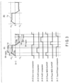
- FIG. 3 is a timing chart showing signal waveforms particularly in the case of driving the optical modulation element 29 with the full tone executed by the liquid crystal optical modulation device 20.
- a portion indicated by a dotted line represents the waveform of the AC power supply from the commercial power source 21.
- the comparator 23a compares the divided value of 1/20 of the voltage of the AC power supply with the ground level 0 [V], so that, as shown in FIG. 3 (A-2), a comparison result that is "1" level in the positive part of the first half 1/2 cycle of the original AC voltage and "0" level in the negative part of the second half 1/2 cycle is output to the timing generation circuit 24.
- the gate driver 25 turns on the MOSFET 27a of the switching circuit 27 to open it as shown in FIG. 3 (A-5).
- the gate driver 26 keeps off the MOSFET 28a of the switching circuit 28 in the closed state.
- the timing generation circuit 24 turns off the MOSFET 27a of the switching circuit 27 via the gate driver 25 to the closed state.
- the voltage application from the commercial power source 21 to the optical modulation element 29 is cut off, and immediately thereafter, the electric charge flows to the distal end side due to the difference in surface potential between the terminal side and the distal end side, and causes a slight voltage drop.
- the optical modulation element 29 itself is a capacitive load, the electric charge stored in the optical modulation element 29 does not flow to the power supply side and the potential can be maintained.
- the gate driver 26 turns on the MOSFET 28a of the switching circuit 28 to open it as shown in FIG. 3 (A-6).
- the gate driver 25 keeps off the MOSFET 27a of the switching circuit 27 in the closed state.
- the timing generation circuit 24 turns off the MOSFET 28a of the switching circuit 28 via the gate driver 26 to the closed state.
- the voltage application from the commercial power source 21 to the optical modulation element 29 is cut off, and immediately thereafter, the voltage slightly drops.
- the optical modulation element 29 itself is a capacitive load, the electric charge stored in the optical modulation element 29 does not flow to the power supply side and the potential is maintained.
- FIG. 3 (B) The waveform of the terminal-side voltage TV applied to the optical modulation element 29, obtained by the operation of FIG. 3 (A-1), is shown in FIG. 3 (B) .
- the internal power loss by the MOSFETs 27a and 28a constituting the switching circuits 27 and 28 can be minimized.
- the waveform with +Vc corresponding to +70 [V] and -Vc corresponding to -70 [V] has been described as an example.
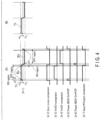
- FIG. 4 is a timing chart showing signal waveforms in the case of performing such half-tone drive.
- a portion indicated by a dotted line represents the waveform of the AC power supplied from the commercial power source 21.
- the MOSFET 28a of the switching circuit 28 is turned on to be an open state, so that the voltage from the commercial power source 21 is supplied to the optical modulation element 29 through the MOSFET 28a and the parasitic diode 27b. Thereafter, the MOSFET 28a is turned off to hold the potential as indicated by a period IVb in FIG. 4 (A-1).
- FIG. 4 (B) The waveform of the terminal-side voltage TV applied to the optical modulation element 29, obtained by the operation of FIG. 4 (A-1), is shown in FIG. 4 (B) .
- FIG. 5 shows respective waveforms of the terminal side voltage TV and the distal end side voltage EV applied to the optical modulation element 29 by opposite phase control in the first operation example as a reference of this operation example.
- the terminal side voltage TV indicated by the solid line in FIG. 5 is applied, so that the voltage value is increased while accumulating charges as shown by hatching in the drawing.
- the distal end side voltage EV indicated by the broken line in the figure is sequentially increased in a delayed phase as compared to the terminal side voltage TV. Even after the voltage of the commercial power source 21 reaches +Vc [V] and the off period starts, the potential rises gradually by the electric charge moving from the terminal side although the degree of rise decreases, as shown in the drawing.
- the difference between the terminal side voltage TV and the distal end side voltage EV becomes smaller as time passes. If the off period is set sufficiently long, there is no difference between the terminal side voltage TV and the distal end side voltage EV.
- the potentials on the terminal side and the distal end side of the optical modulation element 29 converge in the same potential direction after stopping the voltage application. Therefore, as compared to the sine wave drive shown in FIG. 12 , the potential difference between the terminal side voltage and the distal end side voltage can be reduced, and surface unevenness due to the difference in the amount of transmitted light can be reduced.
- the polarity is reversed in the second half of the cycle of the voltage from the commercial power source 21, so that a similar operation is repeated with the reversed polarity, while there is a difference between the terminal side voltage TV and the distal end side voltage EV.
- FIG. 6 shows only the waveforms of the terminal side voltage TV and the distal end side voltage EV extracted from FIG. 5 .
- the size of the area of the hatched portion corresponding to a difference between the terminal side voltage TV shown by the solid line in the drawing and the distal end side voltage EV shown by the broken line in FIG. 6 is considered appears as the difference in degree of the surface unevenness of the transparency on the terminal side and the distal end side in the optical modulation element 29.
- FIG. 7 is a timing chart showing signal waveforms when the liquid crystal optical modulation device 20 operates, in particular when the optical modulation element 29 is driven with fulltone drive in the second operation example of the present embodiment.
- the timing generation circuit 24 is provided with a counter for counting the cycle of the voltage of the commercial power source 21 by the output of the comparator 23a of the zero-cross comparator portion 23. With reference to the count value and the level of the comparator 23a, a thinning operation shown in FIG. 7 (8) (to be described later) is executed.
- a portion indicated by a dotted line represents the waveform of the AC power supplied from the commercial power source 21.
- the comparator 23a compares the divided value of 1/20 of the voltage of the AC power supply with the ground level 0 [V], so that, as shown in FIG. 7 (2), a comparison result that is "1" level in the positive part of the first half 1/2 cycle of the original AC voltage and "0" level in the negative part of the second half 1/2 cycle is output to the timing generation circuit 24.
- the gate driver 25 turns on the MOSFET 27a of the switching circuit 27 to open it as shown in FIG. 7 (6).
- the gate driver 26 keeps off the MOSFET 28a of the switching circuit 28 in the closed state.
- the timing generation circuit 24 turns off the MOSFET 27a of the switching circuit 27 via the gate driver 25 to the closed state.
- the voltage application from the commercial power source 21 to the optical modulation element 29 is cut off.
- the electric charge flows to the distal end side due to the difference in surface potential between the terminal side and the distal end side, and causes a slight voltage drop.
- the optical modulation element 29 itself is a capacitive load, the electric charge stored in the optical modulation element 29 does not flow to the power supply side and the potential can be maintained.
- the operation itself in the first half of the first cycle is equivalent to the first operation example and the contents shown in FIG. 5 .
- the timing generation circuit 24 Upon receipt of the output of the comparator 23a, the timing generation circuit 24 refers to the value “0" of the internal counter and the level of the comparator 23a, and changes the thinning signal from "0" level to "1" level, as shown in FIG. 7 (8).
- the timing generation circuit 24 turns off both the switching circuits 27 and 28 because the thinning signal is at the "1" level.
- the potential state of the optical modulation element 29, which is a capacitive load, is maintained by executing a process of "thinning out” application of a negative voltage from the commercial power source 21.
- the terminal side voltage TV gradually lowers the potential while almost maintaining the potential in the first half of the cycle.
- the distal end side voltage EV gradually raises the potential, though it is lower in value than the terminal side voltage TV. Therefore, the difference between the terminal side voltage TV and the distal end side voltage EV becomes smaller as time passes.
- the timing generation circuit 24 Upon receipt of the output of the comparator 23a, the timing generation circuit 24 increments the value of the internal counter by "+1", and with reference to the level of the comparator 23a, changes the thinning signal from the "1" level to the "0" level, as shown in FIG. 7 (8).
- the timing generation circuit 24 delays the on operation in the switching circuit 27 by the output of the comparator 22a which compares the voltage of the commercial power source 21 with the potential of the optical modulation element 29, and holds the potential of the optical modulation element 29.
- the switching circuit 27 is turned on via the gate driver 25. Until the voltage from the commercial power source 21 reaches +Vc [V], a positive voltage is additionally applied to the optical modulation element 29.
- the terminal side voltage TV is increased again for a short time in the first half of the second cycle.
- the terminal side voltage TV slightly drops immediately after the application is stopped, but maintains a potential higher than that in the first cycle.
- the potential of the distal end side voltage EV is further increased when the on operation starts, and is then gradually raised. Accordingly, the difference with the distal end side voltage TV becomes smaller than that in the first period.
- the timing generation circuit 24 executes processing to thin out the application of the negative voltage to the optical modulation element 29 with reference to the count value of the counter in the timing generation circuit 24 and the level of the comparator 23a.
- the terminal side voltage TV maintains a potential closer to +Vc [V] than that in the first cycle, while the distal end side voltage EV also maintains a potential closer to the value of the terminal side voltage TV.
- the application of voltage is performed only for a short period of time until the supply voltage from the optical modulation element 29 becomes +Vc [V] after it becomes equal to the potential of the optical modulation element 29 in the first half of the cycle.
- the terminal side voltage TV is further increased in this short on-operation period, and slightly decreases immediately after the application is stopped, but maintains a potential closer to +Vc [V] than in the second cycle. Also, the distal end side voltage EV further increases the potential during the on-operation period and gradually increases the potential thereafter. As a result, the difference with the terminal side voltage TV is much smaller than in the second cycle.
- the distal end side voltage EV is approximately equal to the terminal side voltage TV, while the terminal voltage TV maintains a potential closer to +Vc [V] than in the second cycle.
- the timing generation circuit 24 refers to the count value "3" of the internal counter and the level of the comparator 23a, and sets the thinning signal to the "1" level, as shown in FIG. 7 (8), even during the period in which the positive voltage is applied from the commercial power source 21, so that the application of the voltage for turning off the switching circuit 27 is temporarily stopped, and as indicated by the period VII in FIG. 7 (A), the potential at the optical modulation element 29 is maintained.
- the timing generation circuit 24 controls the on operation of the switching circuit 28, so that the same drive as described above with a negative voltage is performed for 3.5 cycles.
- the drive frequency for AC driving the optical modulation element 29 is significantly reduced by the thinning process.
- a flicker may be easily recognized.
- a MOSFET is used as a switching element of the switching circuit, and the rectifying action of a parasitic diode of the MOSFET is used as an example.
- the present invention is not limited to this embodiment.
- a bipolar transistor, an IGBT, a SiCFET, or a GaNFET can also be used as a configuration that can exhibit the same function.
- a rectifying element associated with the switching element for example, a PN junction diode, a Schottky diode, a fast recovery diode, a SiC diode, a GaN diode, a MOSFET diode or the like may be used.
- the polymer dispersed-type liquid crystal in the normal mode is used, which is in the opaque diffusion state when no voltage is applied, and increases the transparency as needed when the voltage is applied.
- the present invention can be similarly applied to a polymer dispersed-type liquid crystal in the reverse mode, in which the characteristics are reverse to those in the normal mode.
- liquid crystal device using a polymer dispersed liquid crystal
- the liquid crystal element may have a configuration in which a polarizing plate and an alignment film are provided at both ends of the liquid crystal layer, and a TN (Twisted Nematic) system, a VA (Vertical Alignment) system, an IPS (In-Plane Switching) system, or the like can be used.
- TN Transmission Nematic
- VA Very Alignment
- IPS In-Plane Switching
- the present invention is applicable not only to the light control glass using a glass substrate, but also to a device using a film made of a synthetic resin material having flexibility.
Landscapes
- Physics & Mathematics (AREA)
- Engineering & Computer Science (AREA)
- General Physics & Mathematics (AREA)
- Crystallography & Structural Chemistry (AREA)
- Chemical & Material Sciences (AREA)
- Theoretical Computer Science (AREA)
- Computer Hardware Design (AREA)
- Nonlinear Science (AREA)
- Mathematical Physics (AREA)
- Optics & Photonics (AREA)
- Liquid Crystal (AREA)
- Circuit Arrangement For Electric Light Sources In General (AREA)
- Optical Modulation, Optical Deflection, Nonlinear Optics, Optical Demodulation, Optical Logic Elements (AREA)
- Liquid Crystal Display Device Control (AREA)
Claims (5)
- Optische Flüssigkristall-Modulationsvorrichtung zur Durchführung eines Lichtsteuerungsantriebs für ein Flüssigkristallpanel (29) mit einem Lichtsteuerungsglas (10), das aus zwei parallelen Plattengläsern (11, 12) gebildet ist, die einen Flüssigkristall (17) vom Polymer-Dispersions-Typ zwischen den Plattengläsern (11, 12) versiegeln, wobei die Vorrichtung umfassteine Eingangsklemme zum Empfangen einer Energieversorgungsspannung von einer kommerziellen Wechselstromquelle (21) und eine Ausgangsklemme zum Versorgen des Flüssigkristallpanels (29) mit der Energieversorgungsspannung;einen ersten Widerstandsspannungsteilungsabschnitt, der aus einem ersten und einem zweiten Widerstand (R31, R32) gebildet ist, die zwischen der Eingangsklemme und Masse in Reihe geschaltet sind, wobei der erste und der zweite Widerstand an einem ersten Verbindungsmittelpunkt miteinander verbunden sind;einen zweiten Widerstandsspannungsteilungsabschnitt, der aus einem dritten und einem vierten Widerstand (R33, R34) gebildet ist, die zwischen der Ausgangsklemme und der Masse in Reihe geschaltet sind, wobei der dritte und der vierte Widerstand an einem zweiten Verbindungsmittelpunkt miteinander verbunden sind; undeinen Spannungsbegrenzungsabschnitt (27, 28) zum Begrenzen der Energieversorgungsspannung, die von der kommerziellen Wechselstromquelle (21) an das Flüssigkristallpanel (29) angelegt wird, wobei der Spannungsbegrenzungsabschnitt umfasst:
ein erstes Schaltelement (27a), das zwischen der Eingangsklemme und einem Knoten geschaltet ist, ein zweites Schaltelement (28a), das zwischen dem Knoten und der Ausgangsklemme geschaltet ist, eine erste Diode (D+) mit einer Anode und einer Kathode, die jeweils mit dem Knoten und der Eingangsklemme verbunden sind, und eine zweite Diode (D-) mit einer Anode und einer Kathode, die jeweils mit dem Knoten und der Ausgangsklemme verbunden sind;wobei die Modulationsvorrichtung ferner umfasst:einen Steuerungsabschnitt (22-26), der dazu eingerichtet ist:in einer Phase innerhalb eines 1/4-Zyklus eines Anstiegs von einem Nulldurchgangspunkt der Energieversorgungsspannung der kommerziellen Wechselstromquelle das erste Schaltelement (27a) einzuschalten, wenn ein Absolutwert der Energieversorgungsspannung gleich wie oder niedriger als eine Grenzspannung ist, um die Energieversorgungsspannung über das erste Schaltelement (27a) und die zweite Diode (D-) an das Flüssigkristallpanel (29) anzulegen; und das erste Schaltelement (27a) auszuschalten, wenn der Absolutwert der Energieversorgungsspannung die Grenzspannung überschreitet;in einer Phase innerhalb eines 1/4-Zyklus eines Abfalls vom Nulldurchgangspunkt der Energieversorgungsspannung der kommerziellen Wechselstromquelle das zweite Schaltelement (28a) einzuschalten, wenn der Absolutwert der Energieversorgungsspannung gleich wie oder niedriger als die Grenzspannung ist, um die Energieversorgungsspannung über die erste Diode (D+) und das zweite Schaltelement (28a) an das Flüssigkristallpanel (29) anzulegen, und das zweite Schaltelement (28a) auszuschalten, wenn der Absolutwert der Energieversorgungsspannung die Grenzspannung überschreitet;wobei der Steuerungsabschnitt umfasst:eine erste DC-Energieversorgung (22d), die dazu eingerichtet ist, eine erste Referenzspannung (VrefC+) auszugeben;eine zweite DC-Energieversorgung (22e), die dazu eingerichtet ist, eine zweite Referenzspannung (VrefC-) auszugeben, wobei die erste Referenzspannung und die zweite Referenzspannung den gleichen Absolutwert aufweisen, aber in ihrer Polarität entgegengesetzt sind;einen ersten Komparator (22a), einen zweiten Komparator (22b), einen dritten Komparator (22c) und einen vierten Komparator (23a), wobei:der erste Verbindungsmittelpunkt mit einem Plus-Eingang des ersten, zweiten und vierten Komparators verbunden ist und ferner mit einem Minus-Eingang des dritten Komparators verbunden ist;der zweite Verbindungsmittelpunkt mit einem Minus-Eingang des ersten Komparators verbunden ist;ein Minus-Eingang des zweiten Komparators dazu eingerichtet ist, die erste Referenzspannung (VrefC+) zu empfangen;ein Plus-Eingang des dritten Komparators dazu eingerichtet ist, die zweite Referenzspannung (VrefC-) zu empfangen;ein Minus-Eingang des vierten Komparators mit der Masse verbunden ist;wobei der Steuerungsabschnitt ferner umfasst:eine Timing-Erzeugungsschaltung (24), die erste bis vierte Eingänge umfasst, die jeweils mit Ausgängen des ersten bis vierten Komparators verbunden sind, und erste und zweite Ausgänge umfasst;einen ersten Gate-Treiber (25) mit einem Eingang, der mit dem ersten Ausgang der Timing-Erzeugungsschaltung (24) verbunden ist, und einem Ausgang, der mit einer Steuerungsklemme des ersten Schaltelements (27a) verbunden ist, undeinen zweiten Gate-Treiber (26) mit einem Eingang, der mit dem zweiten Ausgang der Timing-Erzeugungsschaltung (24) verbunden ist, und einem Ausgang, der mit einer Steuerungsklemme des zweiten Schaltelements (28a) verbunden ist. - Optische Flüssigkristall-Modulationsvorrichtung nach Anspruch 1, wobei der Steuerungsabschnitt (22 - 26) dazu eingerichtet ist, die ersten und zweiten Referenzspannungen (VrefC+, VrefC-) variabel einzustellen.
- Optische Flüssigkristall-Modulationsvorrichtung nach Anspruch 1, wobei jedes der ersten und zweiten Schaltelemente des Spannungsbegrenzungsabschnitts (27, 28) eines von einem Bipolartransistor, einem MOSFET, einem IGBT, einem SiCFET und einem GaNFET ist.
- Optische Flüssigkristall-Modulationsvorrichtung nach Anspruch 1, wobei jede der ersten und zweiten Dioden des Spannungsbegrenzungsabschnitts (27, 28) eine von einer PN-Übergangsdiode, einer Schottky-Diode, einer Fast-Recovery-Diode, einer SiC-Diode, einer GaN-Diode oder einer MOSFET-Diode ist.
- Verfahren zum Betreiben der optischen Flüssigkristall-Modulationsvorrichtung nach Anspruch 1 zur Begrenzung einer an ein Flüssigkristallpanel (29) von einer kommerziellen Wechselstromquelle (21) angelegten Energieversorgungsspannung, wobei das Verfahren durch den Steuerungsabschnitt Folgendes umfasst:Einschalten des ersten Schaltelements (27a) in einer Phase innerhalb eines 1/4-Zyklus eines Anstiegs von einem Nulldurchgangspunkt der Energieversorgungsspannung der kommerziellen Wechselstromquelle, wenn ein Absolutwert der Energieversorgungsspannung gleich wie oder niedriger als eine Grenzspannung ist, um die Energieversorgungsspannung über das erste Schaltelement (27a) und die zweite Diode (D-) an die Flüssigkristallpanel (29) anzulegen; oder Ausschalten des ersten Schaltelements (27a), wenn der Absolutwert der Energieversorgungsspannung die Grenzspannung überschreitet;Einschalten des zweiten Schaltelements (28a) in einer Phase innerhalb eines 1/4-Zyklus eines Abfalls vom Nulldurchgangspunkt der Energieversorgungsspannung der kommerziellen Wechselstromquelle, wenn der Absolutwert der Energieversorgungsspannung gleich oder niedriger als die Grenzspannung ist, um die Versorgungsspannung über die erste Diode (D+) und das zweite Schaltelement (28a) an das Flüssigkristallpanel (29) anzulegen, und Ausschalten des zweiten Schaltelements (28a), wenn der Absolutwert der Energieversorgungsspannung die Grenzspannung überschreitet.
Applications Claiming Priority (2)
| Application Number | Priority Date | Filing Date | Title |
|---|---|---|---|
| JP2017079741A JP6965552B2 (ja) | 2017-04-13 | 2017-04-13 | 液晶調光装置及び液晶調光方法 |
| PCT/JP2018/015430 WO2018190404A1 (ja) | 2017-04-13 | 2018-04-12 | 液晶調光装置及び液晶調光方法 |
Publications (3)
| Publication Number | Publication Date |
|---|---|
| EP3611559A1 EP3611559A1 (de) | 2020-02-19 |
| EP3611559A4 EP3611559A4 (de) | 2020-08-19 |
| EP3611559B1 true EP3611559B1 (de) | 2023-11-15 |
Family
ID=63793265
Family Applications (1)
| Application Number | Title | Priority Date | Filing Date |
|---|---|---|---|
| EP18783764.6A Active EP3611559B1 (de) | 2017-04-13 | 2018-04-12 | Flüssigkristalllichtanpassungsvorrichtung und flüssigkristalllichtanpassungsverfahren |
Country Status (5)
| Country | Link |
|---|---|
| US (1) | US10971106B2 (de) |
| EP (1) | EP3611559B1 (de) |
| JP (1) | JP6965552B2 (de) |
| CN (1) | CN110494797B (de) |
| WO (1) | WO2018190404A1 (de) |
Families Citing this family (2)
| Publication number | Priority date | Publication date | Assignee | Title |
|---|---|---|---|---|
| JP6733747B2 (ja) * | 2017-02-02 | 2020-08-05 | 凸版印刷株式会社 | 調光装置 |
| JP7383227B2 (ja) * | 2019-10-23 | 2023-11-20 | Toppanホールディングス株式会社 | 調光シート、および、調光装置 |
Citations (1)
| Publication number | Priority date | Publication date | Assignee | Title |
|---|---|---|---|---|
| JPS6449924U (de) * | 1987-09-24 | 1989-03-28 |
Family Cites Families (10)
| Publication number | Priority date | Publication date | Assignee | Title |
|---|---|---|---|---|
| JPS6449924A (en) | 1987-08-20 | 1989-02-27 | Teraoka Seiko Kk | Strain gage type load cell |
| KR101224459B1 (ko) * | 2007-06-28 | 2013-01-22 | 엘지디스플레이 주식회사 | 액정표시장치 |
| US10288915B2 (en) * | 2010-09-27 | 2019-05-14 | Gauzy Ltd. | Dimmer and switch suitable for driving a capacitive or complex capacitive-resistive load such as liquid crystal film |
| WO2012161022A1 (ja) * | 2011-05-20 | 2012-11-29 | シャープ株式会社 | 表示装置、液晶表示装置、および駆動方法 |
| KR102041936B1 (ko) | 2011-06-09 | 2019-11-07 | 케이스 웨스턴 리저브 유니버시티 | 광학적 정보 스토리지 매체 |
| JP2013072895A (ja) * | 2011-09-26 | 2013-04-22 | Seiko Electric Co Ltd | 液晶調光装置及び液晶調光素子の駆動装置 |
| US9756694B2 (en) * | 2013-10-31 | 2017-09-05 | Abl Ip Holding Llc | Analog circuit for color change dimming |
| CN105259679B (zh) * | 2015-09-11 | 2018-11-23 | 京东方科技集团股份有限公司 | 电控调光薄膜、其制备方法及显示器件 |
| CN105604455A (zh) * | 2016-01-28 | 2016-05-25 | 衢州学院 | 一种环保智能玻璃 |
| JP6733747B2 (ja) * | 2017-02-02 | 2020-08-05 | 凸版印刷株式会社 | 調光装置 |
-
2017
- 2017-04-13 JP JP2017079741A patent/JP6965552B2/ja active Active
-
2018
- 2018-04-12 EP EP18783764.6A patent/EP3611559B1/de active Active
- 2018-04-12 WO PCT/JP2018/015430 patent/WO2018190404A1/ja not_active Ceased
- 2018-04-12 CN CN201880024464.2A patent/CN110494797B/zh active Active
-
2019
- 2019-10-11 US US16/599,760 patent/US10971106B2/en active Active
Patent Citations (1)
| Publication number | Priority date | Publication date | Assignee | Title |
|---|---|---|---|---|
| JPS6449924U (de) * | 1987-09-24 | 1989-03-28 |
Also Published As
| Publication number | Publication date |
|---|---|
| EP3611559A4 (de) | 2020-08-19 |
| WO2018190404A1 (ja) | 2018-10-18 |
| JP2018180284A (ja) | 2018-11-15 |
| CN110494797A (zh) | 2019-11-22 |
| EP3611559A1 (de) | 2020-02-19 |
| CN110494797B (zh) | 2022-07-26 |
| JP6965552B2 (ja) | 2021-11-10 |
| US10971106B2 (en) | 2021-04-06 |
| US20200043438A1 (en) | 2020-02-06 |
Similar Documents
| Publication | Publication Date | Title |
|---|---|---|
| EP3579045B1 (de) | Dimmvorrichtung | |
| US11467436B2 (en) | Drive circuit and drive method for dimming glass, and dimming glass device | |
| CN109410880B (zh) | 显示面板驱动电路 | |
| US6590552B1 (en) | Method of driving liquid crystal display device | |
| US9095024B1 (en) | Backlight driving circuit and method for reducing soft-start time thereof | |
| US10290262B2 (en) | Scanning drive circuit and flat display device | |
| KR20120110387A (ko) | 화소 회로 및 화소 회로의 구동 방법 | |
| CN101621870A (zh) | 用于驱动背光单元的光源的装置和方法 | |
| US11143890B2 (en) | Liquid crystal optical modulation device and liquid crystal optical modulation method | |
| US10871668B2 (en) | Light control device | |
| CN215770465U (zh) | 显示驱动电路及显示装置 | |
| US10971106B2 (en) | Liquid crystal optical modulation device and liquid crystal optical modulation method | |
| WO2017177486A1 (zh) | 阵列基板及液晶显示面板 | |
| CN102081910A (zh) | 聚合物分散型液晶膜的驱动方法及电路 | |
| JP7226510B2 (ja) | 調光装置 | |
| US9433059B2 (en) | Boost circuits, LED backlight driving circuits and liquid crystal devices | |
| CN202363082U (zh) | 一种高对比度ccfl背光源驱动电路 | |
| CN109493808A (zh) | 显示装置 | |
| KR100757035B1 (ko) | 인버터 구동용 컨트롤러의 위상 제어회로 | |
| CN104505026A (zh) | 灰度电压调节电路及相关电路和装置 | |
| KR19990059986A (ko) | 전하 펌핑회로를 이용한 게이트 온 전압 발생기 | |
| KR20070071338A (ko) | 평판표시장치용 인버터 구동방법 |
Legal Events
| Date | Code | Title | Description |
|---|---|---|---|
| STAA | Information on the status of an ep patent application or granted ep patent |
Free format text: STATUS: THE INTERNATIONAL PUBLICATION HAS BEEN MADE |
|
| PUAI | Public reference made under article 153(3) epc to a published international application that has entered the european phase |
Free format text: ORIGINAL CODE: 0009012 |
|
| STAA | Information on the status of an ep patent application or granted ep patent |
Free format text: STATUS: REQUEST FOR EXAMINATION WAS MADE |
|
| 17P | Request for examination filed |
Effective date: 20191021 |
|
| AK | Designated contracting states |
Kind code of ref document: A1 Designated state(s): AL AT BE BG CH CY CZ DE DK EE ES FI FR GB GR HR HU IE IS IT LI LT LU LV MC MK MT NL NO PL PT RO RS SE SI SK SM TR |
|
| AX | Request for extension of the european patent |
Extension state: BA ME |
|
| DAV | Request for validation of the european patent (deleted) | ||
| DAX | Request for extension of the european patent (deleted) | ||
| A4 | Supplementary search report drawn up and despatched |
Effective date: 20200720 |
|
| RIC1 | Information provided on ipc code assigned before grant |
Ipc: G02F 1/1334 20060101ALI20200714BHEP Ipc: G02F 1/133 20060101ALI20200714BHEP Ipc: G02F 1/13 20060101AFI20200714BHEP |
|
| STAA | Information on the status of an ep patent application or granted ep patent |
Free format text: STATUS: EXAMINATION IS IN PROGRESS |
|
| 17Q | First examination report despatched |
Effective date: 20211007 |
|
| GRAP | Despatch of communication of intention to grant a patent |
Free format text: ORIGINAL CODE: EPIDOSNIGR1 |
|
| STAA | Information on the status of an ep patent application or granted ep patent |
Free format text: STATUS: GRANT OF PATENT IS INTENDED |
|
| INTG | Intention to grant announced |
Effective date: 20230613 |
|
| GRAS | Grant fee paid |
Free format text: ORIGINAL CODE: EPIDOSNIGR3 |
|
| GRAA | (expected) grant |
Free format text: ORIGINAL CODE: 0009210 |
|
| STAA | Information on the status of an ep patent application or granted ep patent |
Free format text: STATUS: THE PATENT HAS BEEN GRANTED |
|
| AK | Designated contracting states |
Kind code of ref document: B1 Designated state(s): AL AT BE BG CH CY CZ DE DK EE ES FI FR GB GR HR HU IE IS IT LI LT LU LV MC MK MT NL NO PL PT RO RS SE SI SK SM TR |
|
| REG | Reference to a national code |
Ref country code: CH Ref legal event code: EP Ref country code: GB Ref legal event code: FG4D |
|
| REG | Reference to a national code |
Ref country code: DE Ref legal event code: R096 Ref document number: 602018061152 Country of ref document: DE |
|
| REG | Reference to a national code |
Ref country code: IE Ref legal event code: FG4D |
|
| REG | Reference to a national code |
Ref country code: LT Ref legal event code: MG9D |
|
| REG | Reference to a national code |
Ref country code: NL Ref legal event code: MP Effective date: 20231115 |
|
| PG25 | Lapsed in a contracting state [announced via postgrant information from national office to epo] |
Ref country code: GR Free format text: LAPSE BECAUSE OF FAILURE TO SUBMIT A TRANSLATION OF THE DESCRIPTION OR TO PAY THE FEE WITHIN THE PRESCRIBED TIME-LIMIT Effective date: 20240216 |
|
| PG25 | Lapsed in a contracting state [announced via postgrant information from national office to epo] |
Ref country code: IS Free format text: LAPSE BECAUSE OF FAILURE TO SUBMIT A TRANSLATION OF THE DESCRIPTION OR TO PAY THE FEE WITHIN THE PRESCRIBED TIME-LIMIT Effective date: 20240315 |
|
| PG25 | Lapsed in a contracting state [announced via postgrant information from national office to epo] |
Ref country code: LT Free format text: LAPSE BECAUSE OF FAILURE TO SUBMIT A TRANSLATION OF THE DESCRIPTION OR TO PAY THE FEE WITHIN THE PRESCRIBED TIME-LIMIT Effective date: 20231115 |
|
| REG | Reference to a national code |
Ref country code: AT Ref legal event code: MK05 Ref document number: 1632308 Country of ref document: AT Kind code of ref document: T Effective date: 20231115 |
|
| PG25 | Lapsed in a contracting state [announced via postgrant information from national office to epo] |
Ref country code: NL Free format text: LAPSE BECAUSE OF FAILURE TO SUBMIT A TRANSLATION OF THE DESCRIPTION OR TO PAY THE FEE WITHIN THE PRESCRIBED TIME-LIMIT Effective date: 20231115 |
|
| PG25 | Lapsed in a contracting state [announced via postgrant information from national office to epo] |
Ref country code: AT Free format text: LAPSE BECAUSE OF FAILURE TO SUBMIT A TRANSLATION OF THE DESCRIPTION OR TO PAY THE FEE WITHIN THE PRESCRIBED TIME-LIMIT Effective date: 20231115 |
|
| PG25 | Lapsed in a contracting state [announced via postgrant information from national office to epo] |
Ref country code: ES Free format text: LAPSE BECAUSE OF FAILURE TO SUBMIT A TRANSLATION OF THE DESCRIPTION OR TO PAY THE FEE WITHIN THE PRESCRIBED TIME-LIMIT Effective date: 20231115 |
|
| PG25 | Lapsed in a contracting state [announced via postgrant information from national office to epo] |
Ref country code: NL Free format text: LAPSE BECAUSE OF FAILURE TO SUBMIT A TRANSLATION OF THE DESCRIPTION OR TO PAY THE FEE WITHIN THE PRESCRIBED TIME-LIMIT Effective date: 20231115 Ref country code: LT Free format text: LAPSE BECAUSE OF FAILURE TO SUBMIT A TRANSLATION OF THE DESCRIPTION OR TO PAY THE FEE WITHIN THE PRESCRIBED TIME-LIMIT Effective date: 20231115 Ref country code: IS Free format text: LAPSE BECAUSE OF FAILURE TO SUBMIT A TRANSLATION OF THE DESCRIPTION OR TO PAY THE FEE WITHIN THE PRESCRIBED TIME-LIMIT Effective date: 20240315 Ref country code: GR Free format text: LAPSE BECAUSE OF FAILURE TO SUBMIT A TRANSLATION OF THE DESCRIPTION OR TO PAY THE FEE WITHIN THE PRESCRIBED TIME-LIMIT Effective date: 20240216 Ref country code: ES Free format text: LAPSE BECAUSE OF FAILURE TO SUBMIT A TRANSLATION OF THE DESCRIPTION OR TO PAY THE FEE WITHIN THE PRESCRIBED TIME-LIMIT Effective date: 20231115 Ref country code: BG Free format text: LAPSE BECAUSE OF FAILURE TO SUBMIT A TRANSLATION OF THE DESCRIPTION OR TO PAY THE FEE WITHIN THE PRESCRIBED TIME-LIMIT Effective date: 20240215 Ref country code: AT Free format text: LAPSE BECAUSE OF FAILURE TO SUBMIT A TRANSLATION OF THE DESCRIPTION OR TO PAY THE FEE WITHIN THE PRESCRIBED TIME-LIMIT Effective date: 20231115 Ref country code: PT Free format text: LAPSE BECAUSE OF FAILURE TO SUBMIT A TRANSLATION OF THE DESCRIPTION OR TO PAY THE FEE WITHIN THE PRESCRIBED TIME-LIMIT Effective date: 20240315 |
|
| PG25 | Lapsed in a contracting state [announced via postgrant information from national office to epo] |
Ref country code: SE Free format text: LAPSE BECAUSE OF FAILURE TO SUBMIT A TRANSLATION OF THE DESCRIPTION OR TO PAY THE FEE WITHIN THE PRESCRIBED TIME-LIMIT Effective date: 20231115 Ref country code: RS Free format text: LAPSE BECAUSE OF FAILURE TO SUBMIT A TRANSLATION OF THE DESCRIPTION OR TO PAY THE FEE WITHIN THE PRESCRIBED TIME-LIMIT Effective date: 20231115 Ref country code: PL Free format text: LAPSE BECAUSE OF FAILURE TO SUBMIT A TRANSLATION OF THE DESCRIPTION OR TO PAY THE FEE WITHIN THE PRESCRIBED TIME-LIMIT Effective date: 20231115 Ref country code: NO Free format text: LAPSE BECAUSE OF FAILURE TO SUBMIT A TRANSLATION OF THE DESCRIPTION OR TO PAY THE FEE WITHIN THE PRESCRIBED TIME-LIMIT Effective date: 20240215 Ref country code: LV Free format text: LAPSE BECAUSE OF FAILURE TO SUBMIT A TRANSLATION OF THE DESCRIPTION OR TO PAY THE FEE WITHIN THE PRESCRIBED TIME-LIMIT Effective date: 20231115 Ref country code: HR Free format text: LAPSE BECAUSE OF FAILURE TO SUBMIT A TRANSLATION OF THE DESCRIPTION OR TO PAY THE FEE WITHIN THE PRESCRIBED TIME-LIMIT Effective date: 20231115 |
|
| PG25 | Lapsed in a contracting state [announced via postgrant information from national office to epo] |
Ref country code: DK Free format text: LAPSE BECAUSE OF FAILURE TO SUBMIT A TRANSLATION OF THE DESCRIPTION OR TO PAY THE FEE WITHIN THE PRESCRIBED TIME-LIMIT Effective date: 20231115 |
|
| PG25 | Lapsed in a contracting state [announced via postgrant information from national office to epo] |
Ref country code: CZ Free format text: LAPSE BECAUSE OF FAILURE TO SUBMIT A TRANSLATION OF THE DESCRIPTION OR TO PAY THE FEE WITHIN THE PRESCRIBED TIME-LIMIT Effective date: 20231115 |
|
| PG25 | Lapsed in a contracting state [announced via postgrant information from national office to epo] |
Ref country code: SK Free format text: LAPSE BECAUSE OF FAILURE TO SUBMIT A TRANSLATION OF THE DESCRIPTION OR TO PAY THE FEE WITHIN THE PRESCRIBED TIME-LIMIT Effective date: 20231115 |
|
| PG25 | Lapsed in a contracting state [announced via postgrant information from national office to epo] |
Ref country code: SM Free format text: LAPSE BECAUSE OF FAILURE TO SUBMIT A TRANSLATION OF THE DESCRIPTION OR TO PAY THE FEE WITHIN THE PRESCRIBED TIME-LIMIT Effective date: 20231115 Ref country code: SK Free format text: LAPSE BECAUSE OF FAILURE TO SUBMIT A TRANSLATION OF THE DESCRIPTION OR TO PAY THE FEE WITHIN THE PRESCRIBED TIME-LIMIT Effective date: 20231115 Ref country code: RO Free format text: LAPSE BECAUSE OF FAILURE TO SUBMIT A TRANSLATION OF THE DESCRIPTION OR TO PAY THE FEE WITHIN THE PRESCRIBED TIME-LIMIT Effective date: 20231115 Ref country code: IT Free format text: LAPSE BECAUSE OF FAILURE TO SUBMIT A TRANSLATION OF THE DESCRIPTION OR TO PAY THE FEE WITHIN THE PRESCRIBED TIME-LIMIT Effective date: 20231115 Ref country code: EE Free format text: LAPSE BECAUSE OF FAILURE TO SUBMIT A TRANSLATION OF THE DESCRIPTION OR TO PAY THE FEE WITHIN THE PRESCRIBED TIME-LIMIT Effective date: 20231115 Ref country code: DK Free format text: LAPSE BECAUSE OF FAILURE TO SUBMIT A TRANSLATION OF THE DESCRIPTION OR TO PAY THE FEE WITHIN THE PRESCRIBED TIME-LIMIT Effective date: 20231115 Ref country code: CZ Free format text: LAPSE BECAUSE OF FAILURE TO SUBMIT A TRANSLATION OF THE DESCRIPTION OR TO PAY THE FEE WITHIN THE PRESCRIBED TIME-LIMIT Effective date: 20231115 |
|
| REG | Reference to a national code |
Ref country code: DE Ref legal event code: R097 Ref document number: 602018061152 Country of ref document: DE |
|
| PLBE | No opposition filed within time limit |
Free format text: ORIGINAL CODE: 0009261 |
|
| STAA | Information on the status of an ep patent application or granted ep patent |
Free format text: STATUS: NO OPPOSITION FILED WITHIN TIME LIMIT |
|
| 26N | No opposition filed |
Effective date: 20240819 |
|
| PG25 | Lapsed in a contracting state [announced via postgrant information from national office to epo] |
Ref country code: SI Free format text: LAPSE BECAUSE OF FAILURE TO SUBMIT A TRANSLATION OF THE DESCRIPTION OR TO PAY THE FEE WITHIN THE PRESCRIBED TIME-LIMIT Effective date: 20231115 |
|
| PG25 | Lapsed in a contracting state [announced via postgrant information from national office to epo] |
Ref country code: SI Free format text: LAPSE BECAUSE OF FAILURE TO SUBMIT A TRANSLATION OF THE DESCRIPTION OR TO PAY THE FEE WITHIN THE PRESCRIBED TIME-LIMIT Effective date: 20231115 |
|
| PG25 | Lapsed in a contracting state [announced via postgrant information from national office to epo] |
Ref country code: MC Free format text: LAPSE BECAUSE OF FAILURE TO SUBMIT A TRANSLATION OF THE DESCRIPTION OR TO PAY THE FEE WITHIN THE PRESCRIBED TIME-LIMIT Effective date: 20231115 |
|
| PG25 | Lapsed in a contracting state [announced via postgrant information from national office to epo] |
Ref country code: MC Free format text: LAPSE BECAUSE OF FAILURE TO SUBMIT A TRANSLATION OF THE DESCRIPTION OR TO PAY THE FEE WITHIN THE PRESCRIBED TIME-LIMIT Effective date: 20231115 |
|
| REG | Reference to a national code |
Ref country code: CH Ref legal event code: PL |
|
| PG25 | Lapsed in a contracting state [announced via postgrant information from national office to epo] |
Ref country code: LU Free format text: LAPSE BECAUSE OF NON-PAYMENT OF DUE FEES Effective date: 20240412 |
|
| GBPC | Gb: european patent ceased through non-payment of renewal fee |
Effective date: 20240412 |
|
| REG | Reference to a national code |
Ref country code: BE Ref legal event code: MM Effective date: 20240430 |
|
| PG25 | Lapsed in a contracting state [announced via postgrant information from national office to epo] |
Ref country code: LU Free format text: LAPSE BECAUSE OF NON-PAYMENT OF DUE FEES Effective date: 20240412 |
|
| PG25 | Lapsed in a contracting state [announced via postgrant information from national office to epo] |
Ref country code: BE Free format text: LAPSE BECAUSE OF NON-PAYMENT OF DUE FEES Effective date: 20240430 |
|
| PG25 | Lapsed in a contracting state [announced via postgrant information from national office to epo] |
Ref country code: GB Free format text: LAPSE BECAUSE OF NON-PAYMENT OF DUE FEES Effective date: 20240412 |
|
| PG25 | Lapsed in a contracting state [announced via postgrant information from national office to epo] |
Ref country code: FR Free format text: LAPSE BECAUSE OF NON-PAYMENT OF DUE FEES Effective date: 20240430 |
|
| PG25 | Lapsed in a contracting state [announced via postgrant information from national office to epo] |
Ref country code: GB Free format text: LAPSE BECAUSE OF NON-PAYMENT OF DUE FEES Effective date: 20240412 Ref country code: FR Free format text: LAPSE BECAUSE OF NON-PAYMENT OF DUE FEES Effective date: 20240430 Ref country code: BE Free format text: LAPSE BECAUSE OF NON-PAYMENT OF DUE FEES Effective date: 20240430 Ref country code: CH Free format text: LAPSE BECAUSE OF NON-PAYMENT OF DUE FEES Effective date: 20240430 |
|
| PG25 | Lapsed in a contracting state [announced via postgrant information from national office to epo] |
Ref country code: IE Free format text: LAPSE BECAUSE OF NON-PAYMENT OF DUE FEES Effective date: 20240412 |
|
| PGFP | Annual fee paid to national office [announced via postgrant information from national office to epo] |
Ref country code: DE Payment date: 20250305 Year of fee payment: 8 |
|
| PG25 | Lapsed in a contracting state [announced via postgrant information from national office to epo] |
Ref country code: CY Free format text: LAPSE BECAUSE OF FAILURE TO SUBMIT A TRANSLATION OF THE DESCRIPTION OR TO PAY THE FEE WITHIN THE PRESCRIBED TIME-LIMIT; INVALID AB INITIO Effective date: 20180412 |
|
| PG25 | Lapsed in a contracting state [announced via postgrant information from national office to epo] |
Ref country code: HU Free format text: LAPSE BECAUSE OF FAILURE TO SUBMIT A TRANSLATION OF THE DESCRIPTION OR TO PAY THE FEE WITHIN THE PRESCRIBED TIME-LIMIT; INVALID AB INITIO Effective date: 20180412 |
|
| PG25 | Lapsed in a contracting state [announced via postgrant information from national office to epo] |
Ref country code: FI Free format text: LAPSE BECAUSE OF FAILURE TO SUBMIT A TRANSLATION OF THE DESCRIPTION OR TO PAY THE FEE WITHIN THE PRESCRIBED TIME-LIMIT Effective date: 20231115 |
|
| PG25 | Lapsed in a contracting state [announced via postgrant information from national office to epo] |
Ref country code: TR Free format text: LAPSE BECAUSE OF FAILURE TO SUBMIT A TRANSLATION OF THE DESCRIPTION OR TO PAY THE FEE WITHIN THE PRESCRIBED TIME-LIMIT Effective date: 20231115 |