EP3614227A2 - Système de régulateur à faible perte à double boucle - Google Patents
Système de régulateur à faible perte à double boucle Download PDFInfo
- Publication number
- EP3614227A2 EP3614227A2 EP19191173.4A EP19191173A EP3614227A2 EP 3614227 A2 EP3614227 A2 EP 3614227A2 EP 19191173 A EP19191173 A EP 19191173A EP 3614227 A2 EP3614227 A2 EP 3614227A2
- Authority
- EP
- European Patent Office
- Prior art keywords
- circuit
- output
- coupled
- amplifier circuit
- amplifier
- Prior art date
- Legal status (The legal status is an assumption and is not a legal conclusion. Google has not performed a legal analysis and makes no representation as to the accuracy of the status listed.)
- Granted
Links
Images


Classifications
-
- G—PHYSICS
- G05—CONTROLLING; REGULATING
- G05F—SYSTEMS FOR REGULATING ELECTRIC OR MAGNETIC VARIABLES
- G05F3/00—Non-retroactive systems for regulating electric variables by using an uncontrolled element, or an uncontrolled combination of elements, such element or such combination having self-regulating properties
- G05F3/02—Regulating voltage or current
- G05F3/08—Regulating voltage or current wherein the variable is DC
- G05F3/10—Regulating voltage or current wherein the variable is DC using uncontrolled devices with non-linear characteristics
- G05F3/16—Regulating voltage or current wherein the variable is DC using uncontrolled devices with non-linear characteristics being semiconductor devices
- G05F3/20—Regulating voltage or current wherein the variable is DC using uncontrolled devices with non-linear characteristics being semiconductor devices using diode- transistor combinations
- G05F3/26—Current mirrors
-
- G—PHYSICS
- G05—CONTROLLING; REGULATING
- G05F—SYSTEMS FOR REGULATING ELECTRIC OR MAGNETIC VARIABLES
- G05F1/00—Automatic systems in which deviations of an electric quantity from one or more predetermined values are detected at the output of the system and fed back to a device within the system to restore the detected quantity to its predetermined value or values, i.e. retroactive systems
- G05F1/10—Regulating voltage or current
- G05F1/46—Regulating voltage or current wherein the variable actually regulated by the final control device is DC
- G05F1/461—Regulating voltage or current wherein the variable actually regulated by the final control device is DC using an operational amplifier as final control device
-
- G—PHYSICS
- G05—CONTROLLING; REGULATING
- G05F—SYSTEMS FOR REGULATING ELECTRIC OR MAGNETIC VARIABLES
- G05F1/00—Automatic systems in which deviations of an electric quantity from one or more predetermined values are detected at the output of the system and fed back to a device within the system to restore the detected quantity to its predetermined value or values, i.e. retroactive systems
- G05F1/10—Regulating voltage or current
- G05F1/46—Regulating voltage or current wherein the variable actually regulated by the final control device is DC
- G05F1/56—Regulating voltage or current wherein the variable actually regulated by the final control device is DC using semiconductor devices in series with the load as final control devices
- G05F1/565—Regulating voltage or current wherein the variable actually regulated by the final control device is DC using semiconductor devices in series with the load as final control devices sensing a condition of the system or its load in addition to means responsive to deviations in the output of the system, e.g. current, voltage, power factor
-
- G—PHYSICS
- G05—CONTROLLING; REGULATING
- G05F—SYSTEMS FOR REGULATING ELECTRIC OR MAGNETIC VARIABLES
- G05F1/00—Automatic systems in which deviations of an electric quantity from one or more predetermined values are detected at the output of the system and fed back to a device within the system to restore the detected quantity to its predetermined value or values, i.e. retroactive systems
- G05F1/10—Regulating voltage or current
- G05F1/46—Regulating voltage or current wherein the variable actually regulated by the final control device is DC
- G05F1/56—Regulating voltage or current wherein the variable actually regulated by the final control device is DC using semiconductor devices in series with the load as final control devices
- G05F1/575—Regulating voltage or current wherein the variable actually regulated by the final control device is DC using semiconductor devices in series with the load as final control devices characterised by the feedback circuit
Definitions
- This disclosure relates generally to electronic circuits, and more specifically, to a dual loop low dropout (LDO) regulator system.
- LDO loop low dropout
- SoC systems-on-a-chip
- voltage regulators are commonly used to provide a stable voltage to load circuits such as custom switching logic, memories, analog circuits, and so on.
- load circuits can draw a significant amount of peak currents and affect the response and accuracy of the voltage provided by the regulators. Therefore, a need exists for a voltage regulator system that improves voltage response and accuracy when supplying peak currents.
- a dual loop low dropout (LDO) regulator system having a feedback path conditionally enabled.
- the dual loop LDO provides a predetermined output voltage and includes a fast loop for fast settling of the output voltage and a slow loop for accurately setting the output voltage.
- the slow loop incorporates a switch circuit in the feedback path which is enabled when the output voltage is within a predetermined range of the predetermined output voltage value allowing the fast loop to be optimized for speed while providing an accurate output voltage.
- FIG. 1 illustrates, in simplified block diagram form, an example dual loop low dropout (LDO) regulator system 100 in accordance with an embodiment.
- System 100 includes cascaded arrangement of a first amplifier stage 102 and a second amplifier stage 104 coupled to a load circuit 106 by way of an output node labeled VOUT.
- a logic control circuit 108 is coupled to receive output control signals CS1, CS2 from the second amplifier stage 104 and the load circuit 106 and provide a control signal CSOUT to a switch circuit 110 coupled at an input of the first amplifier stage 102.
- the first amplifier stage 102 of system 100 is implemented as an operational amplifier having a non-inverting input (+) coupled to receive a reference voltage labeled VREF, an inverting input (-) coupled to the output node by way of a first feedback path 116, and an output coupled to provide an output voltage signal V1 to the second amplifier stage 104 at node labeled V1.
- the first feedback path 116 includes switch circuit 110 coupled in the path from VOUT to the inverting input of the operational amplifier. When the control signal CSOUT is at a first state (e.g., logic low level), the switch circuit is configured to cause a short circuit providing a contiguous conductive first feedback path 116.
- the switch circuit When CSOUT is at a second state (e.g., logic high level), the switch circuit is configured to open causing an open circuit in the first feedback path 116 and inhibits the VOUT signal from reaching the inverting input.
- a capacitor 112 is coupled at the inverting input to hold a voltage level when the first feedback path 116 is open.
- the first feedback path 116 along with the first amplifier stage 102 form a first loop characterized as a slow loop. When enabled (e.g., switch circuit 110 closed), the slow loop serves to accurately set the output voltage to a predetermined VOUT value.
- the second amplifier stage 104 of system 100 is implemented as a low DC gain, fast settling amplifier including an activity detection circuit.
- the second amplifier stage 104 includes a non-inverting input (+) coupled to receive output voltage signal V1, an inverting input (-) coupled to the output node by way of a second feedback path 114, a first output coupled to provide a regulated output voltage VOUT to the load circuit 106 at node labeled VOUT, and a second output coupled to provide control signal CS1 to logic control circuit 108.
- the second feedback path 114 along with the second operational amplifier form a second loop characterized as a fast loop. The fast loop serves to quickly settle the output voltage to the predetermined VOUT value.
- the CS1 signal provides a fast loop active indication (e.g., second operational amplifier sourcing or sinking current).
- the CS1 signal provides an indication that the second amplifier stage 104 is sourcing or sinking current at or beyond a predetermined threshold (e.g., approximately 10% of a maximum source or sink current value of the second operational amplifier). For example, if the maximum source current value of the second operational amplifier is approximately 1.0 milliamp, then the CS1 signal provides an active indication when predetermined threshold value of approximately 100 microamps is met or exceeded. In other embodiments, other threshold values may be chosen.
- the second feedback path 114 may be implemented within the circuitry of the second amplifier stage 104.
- the load circuit 106 of system 100 includes an input coupled to receive regulated voltage VOUT and an output coupled to provide control signal CS2 to logic control circuit 108.
- the CS2 signal provides a load circuit active indication (e.g., load circuit switching/operating activity).
- the load circuit 106 may include any switching circuitry (e.g., digital-to-analog converter (DAC) circuits, switched-capacitor circuits) which requires a regulated voltage (e.g., VOUT) having an accurate settling behavior.
- the load circuit 106 of system 100 is a capacitive DAC of a successive approximation register (SAR) analog-to-digital converter (ADC).
- the logic control circuit 108 includes a first input coupled to receive control signal CS1, a second input coupled to receive control signal CS2, and an output coupled to provide control signal CSOUT to switch circuit 110.
- the logic control circuit 108 may include one or more logic gates (e.g., OR gate) or combinational logic.
- the logic control circuit 108 is configured to provide control signal CSOUT based on input control signals CS1 and CS2.
- the CSOUT signal is at a first state (e.g., logic low level) causing the switch circuit 110 to close, completing a conduction path (e.g., first feedback path 116) from VOUT to the inverting input (-) of the first amplifier stage 102.
- the control signal CSOUT is at a second state (e.g., logic high level) causing the switch circuit to open which results in an open circuit in the first feedback path 116.
- the switch circuit is implemented as P-channel transistor having a control electrode coupled to receive the CSOUT signal.
- the switch circuit may be implemented as a transmission gate having a P-channel transistor and an N-channel transistor connected in a parallel arrangement. With this arrangement, control electrodes of the P-channel and N-channel transistors are coupled to receive the CSOUT signal and a complement of the CSOUT signal, respectively.
- switch circuit 110 may be implemented using other circuit configurations.
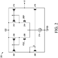
- FIG. 2 illustrates, in simplified schematic diagram form, an example implementation of the first amplifier stage 102 of FIG. 1 in accordance with an embodiment.
- the first amplifier stage circuitry 200 includes a non-inverting input coupled to receive a reference voltage labeled VREF, an inverting input coupled to receive a feedback voltage labeled VOUT (e.g., when switch circuit 110 is closed), and an output coupled to provide output voltage labeled V1.
- the first amplifier stage circuitry 200 includes P-channel transistors 202-204, 210-212, N-channel transistors 206-208, 216-218, and current source 218.
- Transistors 202 and 204 are configured to form a first current mirror having a first current branch and a second current branch.
- a first current electrode of each of transistors 202 and 204 is coupled to a first voltage supply terminal (e.g., VDD).
- a second current electrode of transistor 202 is coupled to a first current electrode and control electrode of transistor 208 in the first current branch and a control electrode of transistor 216 at node labeled D.
- a second current electrode of transistor 204 is coupled to control electrodes of transistors 202, 204 at node labeled A and a first current electrode of transistor 206 in the second current branch.
- a control electrode of transistor 206 serves as the inverting input of first amplifier stage circuitry 200 and is coupled to receive the feedback voltage VOUT when switch circuit 110 is closed.
- Transistors 210 and 212 are configured to form a second current mirror having a third current branch and a fourth current branch.
- a first current electrode of each of transistors 210 and 212 is coupled to the first voltage supply terminal.
- a second current electrode of transistor 210 is coupled to a first current electrode of transistor 216 in the third current branch at output node labeled V1.
- a second current electrode of transistor 212 is coupled to control electrodes of transistors 210 and 212 at node labeled B and a first current electrode of transistor 214 in the fourth current branch.
- a control electrode of transistor 214 serves as the non-inverting input of first amplifier stage circuitry 200 and is coupled to receive the reference voltage VREF.
- a second current electrode of each of transistors 206 and 214 is coupled to a first terminal of current source 218 at node labeled C.
- a second current electrode of each of transistors 208 and 216 and a second terminal of current source 218 are coupled to a second voltage supply terminal (e.g., VSS).
- FIG. 3 illustrates, in simplified schematic diagram form, an example implementation of the second amplifier stage 104 of FIG. 1 in accordance with an embodiment.
- Second amplifier stage circuitry 300 includes an amplifier portion 320 and an activity detection portion 322.
- the activity detection portion 322 is configured to provide an active indication signal (CS1) when the amplifier portion 320 is sourcing or sinking current.
- the second amplifier stage circuitry 300 includes a non-inverting input coupled to receive the V1 voltage signal generated by the first amplifier stage 102, a bias input coupled to receive a bias voltage labeled VBIAS, a first output coupled to provide output voltage VOUT, and a second output coupled to provide the activity indication signal CS1.
- the amplifier portion 320 of the second amplifier stage circuitry 300 includes P-channel transistors 302-304, 308, N-channel transistor 306, and current source 310.
- the activity detection portion 322 of the second amplifier stage circuitry 300 includes P-channel transistor 312, current source 314, and buffer circuit 316.
- transistors 302 and 304 are configured to form a current mirror having a first current branch and a second current branch.
- a first current electrode of each of transistors 302 and 304 is coupled to a first voltage supply terminal (e.g., VDD).
- a second current electrode of transistor 304 is coupled to a first current electrode of transistor 308 in the first current branch at output node labeled VOUT.
- a second current electrode of transistor 302 is coupled to control electrodes of transistors 302 and 304 at node labeled AA and a first current electrode of transistor 306 in the second current branch.
- a control electrode of transistor 306 is coupled to receive a bias voltage labeled VBIAS.
- the circuit for providing the VBIAS voltage (not shown) is included within the second amplifier stage circuitry 300. In other embodiments, the circuit for providing the VBIAS voltage may be located outside of the second amplifier stage circuitry 300.
- a control electrode of transistor 308 serves as the non-inverting input of the second amplifier stage circuitry 300 and is coupled to receive the V1 voltage signal.
- a second current electrode of each of transistors 306 and 308 is coupled to a first terminal of current source 310 at node labeled BB.
- a second terminal of current source 310 is coupled to a second voltage supply terminal (e.g., VSS).
- a first current electrode of transistor 312 is coupled to the first voltage supply terminal and a control electrode of transistor 312 is coupled to the amplifier portion at node AA.
- a second current electrode of transistor 312 is coupled to a first terminal of current source 314 and an input of buffer circuit 316 at node labeled CC.
- a second terminal of current source 314 is coupled to the second voltage supply terminal.
- An output of buffer circuit 316 provides the activity indication signal CS1.
- a feedback path (e.g., second feedback path 114) is essentially formed within the second amplifier stage circuitry 300.
- the control electrode of transistor 308 serves as the non-inverting input (+) of the second amplifier stage circuitry 300 coupled to receive the V1 voltage signal and the first current electrode of transistor 308 (e.g., source) serves as the inverting input (-) coupled to receive the VOUT voltage signal, thus forming the feedback path.
- the amplifier portion 320 including the feedback path form a loop characterized as a fast loop (e.g., fast loop formed by second feedback path 114 along with the second amplifier stage 104 of FIG. 1 ). The fast loop serves to quickly settle the output voltage to a predetermined VOUT value.
- the CS1 signal provides a fast loop active indication (e.g., amplifier portion 320 sourcing or sinking current).
- the CS1 signal provides an indication that the amplifier portion 320 of the second amplifier stage circuitry 300 is sourcing or sinking current at or beyond a predetermined threshold.
- the threshold value is approximately 10% of a maximum source or sink current value of the amplifier portion 320 of the second amplifier stage circuitry 300.
- the CS1 signal provides an active indication (e.g., logic high level signal) when predetermined threshold value of approximately 100 microamps is met or exceeded. In other embodiments, other threshold values may be chosen.
- the second feedback path 114 may be implemented within the circuitry of the second amplifier stage circuitry 300.
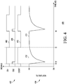
- FIG. 4 illustrates, in plot diagram form, an example simulation result and control signal timing of the dual loop LDO system 100 of FIG. 1 in accordance with an embodiment.
- the plot diagram 400 includes control signal timing 402 and corresponding VOUT simulation response 404.
- the control signal timing 402 shows control signals CS1, CS2, and CSOUT having respective waveforms 406, 408, and 410 during normal operation of system 100.
- the VOUT simulation response 404 shows time values in nanoseconds (nS) on the X-axis, and voltage values in volts on the Y-axis.
- the VOUT simulation response 404 includes plots 412 and 414 depicting simulation results of system 100 during normal operation.
- plot 412 shows a desired (e.g., predetermined, programmed) VOUT output voltage value of 0.9 volts and plot 414 shows VOUT voltage response during periodic activity of load circuit 106.
- desired e.g., predetermined, programmed
- plot 414 shows VOUT voltage response during periodic activity of load circuit 106.
- Control signal CS2 from the load circuit 106 transitions to a logic high level indicating that the load circuit 106 (e.g., capacitive DAC of an SAR ADC) is active.
- the load circuit 106 begins drawing current (e.g., switching activity of sample and evaluation phases of the capacitive DAC).
- the second operational amplifier 104 sources current to the load circuit 106.
- the CS1 signal transitions to a logic high level (e.g., at time t1) providing a fast loop active indication.
- the CSOUT signal is a logical OR of the CS1 and CS2 control signals. Accordingly, the CSOUT signal transitions to a logic high level (e.g., at time t1) when the CS1 signal or the CS2 signal transitions to a logic high level.
- the switch circuit 110 is opened resulting in an open circuit in feedback path 116.
- Capacitor 112 coupled at the inverting input first amplifier stage 102 holds a voltage level while the switch circuit 110 is open. Because the amount of current drawn by the load circuit 106 is momentarily greater than the amount of current sourced by the second amplifier stage 104, the VOUT voltage dips slightly (e.g., about 60 millivolts).
- the load circuit 106 becomes inactive (e.g., sample and evaluation phases of the capacitive DAC are completed) and the CS2 signal transitions to a logic low level.
- the load circuit 106 becomes inactive the VOUT voltage begins to recover toward the desired VOUT voltage value. Because of the capacitive nature of the load circuit 106, current continues to be sourced by the second operational amplifier 104 as the VOUT voltage recovers.
- the CS1 signal transitions to a logic low level indicating that the second amplifier stage 104 is sourcing current below the predetermined threshold. Accordingly, the CSOUT signal transitions to a logic low level.
- the switch circuit 110 is closed completing the feedback path 116 from VOUT to the second input of the first amplifier stages and a resulting V1 voltage signal is provided to the second amplifier stage 104 allowing for accurate return of the VOUT voltage to the desired VOUT voltage value.
- Control signals CS1 and CS2 each transition to a logic high level indicating that the load circuit 106 is active and the second amplifier stage 104 is sourcing current.
- CSOUT transitions to a logic high level causing switch circuit 110 to open which results in an open circuit in feedback path 116.
- the cycle continues as described at times t1 through t3.
- an LDO regulator system including a first amplifier circuit having a first input coupled to receive a reference voltage and an output; a second amplifier circuit having a first input coupled to the output of the first amplifier, the second amplifier circuit configured to provide at a first output a predetermined voltage; and a switch circuit coupled between the first output of the second amplifier circuit and a second input of the first amplifier circuit, the switch circuit configured to cause an open circuit in a first feedback path from the first output of the second amplifier circuit to the second input of the first amplifier circuit based on a control signal.
- the first output of the second amplifier circuit may be coupled directly to a second input of the second amplifier circuit forming a second feedback path.
- the system may further include a capacitor coupled at the second input of the first amplifier circuit.
- the system may further include a load circuit coupled to the first output of the second amplifier circuit, the load circuit configured to provide a first active indication signal when the load circuit is active.
- the load circuit may include a capacitive digital-to-analog converter (DAC).
- the second amplifier circuit may further include a detection circuit configured to provide a second active indication signal at a second output when at least a predetermined amount of current is being sourced by the second amplifier circuit.
- the switch circuit may be configured to cause the first feedback path to have continuity from the first output of the second amplifier circuit to the second input of the first amplifier circuit when the predetermined voltage is provided at the first output.
- the system may further include a control circuit coupled to provide the control signal to the switch circuit, the control circuit coupled to receive the first active indication signal and the second active indication signal.
- the switch circuit may include a P-channel transistor coupled to receive the control signal.
- an LDO regulator system including a first amplifier circuit having a first input coupled to receive a reference voltage and an output; a second amplifier circuit having a first input coupled to the output of the first amplifier, the second amplifier circuit configured to provide at a first output a predetermined voltage; and a switch circuit coupled to receive a control signal, the switch circuit configured to complete a first feedback path from the first output of the second amplifier circuit to a second input of the first amplifier circuit when the control signal is at a first state and to form an open circuit in the first feedback path when the control signal is at a second state.
- the system may further include a capacitor coupled at the second input of the first amplifier circuit.
- the first output of the second amplifier circuit may be coupled directly to a second input of the second amplifier circuit forming a second feedback path.
- the system may further include a load circuit coupled to the first output of the second amplifier circuit, the load circuit configured to provide an active indication signal when the load circuit is active.
- the load circuit may include a capacitive digital-to-analog converter (DAC).
- the second amplifier circuit may further include a detection circuit configured to provide an active indication signal at a second output when an amount of current sourced by the second amplifier circuit exceeds a predetermined threshold.
- the system may further include a control circuit coupled to provide the control signal to the switch circuit.
- an LDO regulator system including a slow loop amplifier circuit having a first input coupled to receive a reference voltage and an output; a fast loop amplifier circuit having a first input coupled to the output of the first amplifier, the fast loop amplifier circuit configured to provide at a first output a predetermined voltage; and a switch circuit configured to complete a first feedback loop from the first output of the fast loop amplifier circuit to a second input of the slow loop amplifier circuit when the fast loop amplifier circuit is not sourcing at least a predetermined amount of current.
- the system may further include a capacitor coupled at the second input of the slow loop amplifier circuit.
- the first output of the fast loop amplifier circuit may be coupled directly to a second input of the fast loop amplifier circuit forming a second feedback loop.
- the system may further include a load circuit coupled to the first output of the fast loop amplifier circuit, the load circuit characterized as a capacitive digital-to-analog converter (DAC).
- DAC capacitive digital-to-analog converter
- the dual loop LDO provides a predetermined output voltage and includes a fast loop for fast settling of the output voltage and a slow loop for accurately setting the output voltage.
- the slow loop incorporates a switch circuit in the feedback path which is enabled when the output voltage is within a predetermined range of the predetermined output voltage value allowing the fast loop to be optimized for speed while providing an accurate output voltage.
- Coupled is not intended to be limited to a direct coupling or a mechanical coupling.
Landscapes
- Engineering & Computer Science (AREA)
- Physics & Mathematics (AREA)
- Electromagnetism (AREA)
- General Physics & Mathematics (AREA)
- Radar, Positioning & Navigation (AREA)
- Automation & Control Theory (AREA)
- Microelectronics & Electronic Packaging (AREA)
- Nonlinear Science (AREA)
- Continuous-Control Power Sources That Use Transistors (AREA)
- Amplifiers (AREA)
Applications Claiming Priority (1)
| Application Number | Priority Date | Filing Date | Title |
|---|---|---|---|
| US16/108,387 US10488875B1 (en) | 2018-08-22 | 2018-08-22 | Dual loop low dropout regulator system |
Publications (3)
| Publication Number | Publication Date |
|---|---|
| EP3614227A2 true EP3614227A2 (fr) | 2020-02-26 |
| EP3614227A3 EP3614227A3 (fr) | 2020-03-04 |
| EP3614227B1 EP3614227B1 (fr) | 2023-01-18 |
Family
ID=67614441
Family Applications (1)
| Application Number | Title | Priority Date | Filing Date |
|---|---|---|---|
| EP19191173.4A Active EP3614227B1 (fr) | 2018-08-22 | 2019-08-12 | Système de régulateur à faible perte à double boucle |
Country Status (3)
| Country | Link |
|---|---|
| US (1) | US10488875B1 (fr) |
| EP (1) | EP3614227B1 (fr) |
| CN (1) | CN110858086B (fr) |
Cited By (1)
| Publication number | Priority date | Publication date | Assignee | Title |
|---|---|---|---|---|
| CN114967826A (zh) * | 2021-02-26 | 2022-08-30 | 瑞昱半导体股份有限公司 | 低压差稳压器 |
Families Citing this family (7)
| Publication number | Priority date | Publication date | Assignee | Title |
|---|---|---|---|---|
| US10803968B2 (en) * | 2019-03-05 | 2020-10-13 | Texas Instruments Incorporated | Methods and apparatus to control switching of a sampling circuit |
| US10958162B1 (en) * | 2019-12-31 | 2021-03-23 | Vidatronic, Inc. | Dual-loop regulated switched capacitor DC-DC converter |
| US11722060B2 (en) | 2020-07-22 | 2023-08-08 | Apple Inc. | Power converter with charge injection from booster rail |
| KR20220044019A (ko) | 2020-09-29 | 2022-04-06 | 삼성전자주식회사 | 로우 드롭아웃 레귤레이터들을 포함하는 전자 장치 |
| US11474550B2 (en) | 2020-11-05 | 2022-10-18 | Samsung Display Co., Ltd. | Dual loop voltage regulator utilizing gain and phase shaping |
| TWI788756B (zh) * | 2021-01-15 | 2023-01-01 | 瑞昱半導體股份有限公司 | 電壓產生電路及相關電容充電方法和系統 |
| CN114815940B (zh) * | 2021-01-22 | 2024-01-30 | 瑞昱半导体股份有限公司 | 电压产生电路及相关电容充电方法和系统 |
Family Cites Families (28)
| Publication number | Priority date | Publication date | Assignee | Title |
|---|---|---|---|---|
| US5283514A (en) * | 1992-09-08 | 1994-02-01 | Hybricon Corporation | Fast response current regulator for DC power supply |
| CN1045494C (zh) * | 1993-08-25 | 1999-10-06 | 陈大可 | 功率开关管驱动信号的平衡控制装置 |
| EP1336912A1 (fr) | 2002-02-18 | 2003-08-20 | Motorola, Inc. | Régulateur de tension à faible tension de déchêt |
| DK1378808T3 (da) * | 2002-07-05 | 2008-06-23 | Dialog Semiconductor Gmbh | LDO-regulator med stort udgangsbelastningsområde og fast intern loop |
| US6765374B1 (en) * | 2003-07-10 | 2004-07-20 | System General Corp. | Low drop-out regulator and an pole-zero cancellation method for the same |
| TWI233543B (en) * | 2003-10-01 | 2005-06-01 | Mediatek Inc | Fast-disabled voltage regulator circuit with low-noise feedback loop |
| TWI263124B (en) * | 2004-11-19 | 2006-10-01 | Sunplus Technology Co Ltd | Voltage regulator circuit with low quiescent current |
| US7327125B2 (en) * | 2005-02-17 | 2008-02-05 | Qualcomm Incorporated | Power supply circuit having voltage control loop and current control loop |
| US7821240B2 (en) | 2005-07-21 | 2010-10-26 | Freescale Semiconductor, Inc. | Voltage regulator with pass transistors carrying different ratios of the total load current and method of operation therefor |
| US8294441B2 (en) * | 2006-11-13 | 2012-10-23 | Decicon, Inc. | Fast low dropout voltage regulator circuit |
| US7907074B2 (en) * | 2007-11-09 | 2011-03-15 | Linear Technology Corporation | Circuits and methods to reduce or eliminate signal-dependent modulation of a reference bias |
| US8754620B2 (en) * | 2009-07-03 | 2014-06-17 | Stmicroelectronics International N.V. | Voltage regulator |
| US8575905B2 (en) * | 2010-06-24 | 2013-11-05 | International Business Machines Corporation | Dual loop voltage regulator with bias voltage capacitor |
| DE102010044924B4 (de) * | 2010-09-10 | 2021-09-16 | Texas Instruments Deutschland Gmbh | Elektronische Vorrichtung und Verfahren für diskrete lastadaptive Spannungsregelung |
| EP2533126B1 (fr) * | 2011-05-25 | 2020-07-08 | Dialog Semiconductor GmbH | Régulateur de tension à faible chute doté d'une commande dynamique de la tension |
| US9110488B2 (en) * | 2011-06-07 | 2015-08-18 | International Business Machines Corporation | Wide-bandwidth linear regulator |
| US8854023B2 (en) * | 2011-08-03 | 2014-10-07 | Texas Instruments Incorporated | Low dropout linear regulator |
| US8716993B2 (en) * | 2011-11-08 | 2014-05-06 | Semiconductor Components Industries, Llc | Low dropout voltage regulator including a bias control circuit |
| US9645591B2 (en) * | 2014-01-09 | 2017-05-09 | Qualcomm Incorporated | Charge sharing linear voltage regulator |
| US9568927B2 (en) * | 2014-05-06 | 2017-02-14 | Stmicroelectronics, Inc. | Current modulation circuit |
| KR102204678B1 (ko) * | 2014-12-11 | 2021-01-20 | 삼성전자주식회사 | 인버터 증폭기 기반의 이중 루프 레귤레이터 및 그에 따른 전압 레귤레이팅 방법 |
| US10108212B2 (en) | 2015-09-22 | 2018-10-23 | Intel Corporation | Digital low drop-out voltage controller including embedded dual-loop feedback for minimum energy point operation |
| US9684325B1 (en) * | 2016-01-28 | 2017-06-20 | Qualcomm Incorporated | Low dropout voltage regulator with improved power supply rejection |
| US9946283B1 (en) * | 2016-10-18 | 2018-04-17 | Qualcomm Incorporated | Fast transient response low-dropout (LDO) regulator |
| CN106406411B (zh) * | 2016-12-08 | 2018-01-02 | 上海爱信诺航芯电子科技有限公司 | 低压差线性稳压器电路及电源 |
| EP3435192B1 (fr) * | 2017-07-28 | 2022-08-24 | NXP USA, Inc. | Puissance ultra faible régulateur de tension linéaire |
| US10234881B1 (en) * | 2017-11-07 | 2019-03-19 | Nxp B.V. | Digitally-assisted capless voltage regulator |
| US10338620B2 (en) * | 2017-11-15 | 2019-07-02 | Infineon Technologies Ag | Feedback circuit for regulation loops |
-
2018
- 2018-08-22 US US16/108,387 patent/US10488875B1/en active Active
-
2019
- 2019-08-12 EP EP19191173.4A patent/EP3614227B1/fr active Active
- 2019-08-21 CN CN201910777085.7A patent/CN110858086B/zh active Active
Cited By (2)
| Publication number | Priority date | Publication date | Assignee | Title |
|---|---|---|---|---|
| CN114967826A (zh) * | 2021-02-26 | 2022-08-30 | 瑞昱半导体股份有限公司 | 低压差稳压器 |
| CN114967826B (zh) * | 2021-02-26 | 2024-04-16 | 瑞昱半导体股份有限公司 | 低压差稳压器 |
Also Published As
| Publication number | Publication date |
|---|---|
| EP3614227B1 (fr) | 2023-01-18 |
| US10488875B1 (en) | 2019-11-26 |
| CN110858086A (zh) | 2020-03-03 |
| EP3614227A3 (fr) | 2020-03-04 |
| CN110858086B (zh) | 2023-02-03 |
Similar Documents
| Publication | Publication Date | Title |
|---|---|---|
| EP3614227B1 (fr) | Système de régulateur à faible perte à double boucle | |
| CN108649939B (zh) | 电源检测电路及方法 | |
| US5440254A (en) | Accurate low voltage detect circuit | |
| DE112018005096T5 (de) | Hochpräzise stromerfassung unter verwendung eines erfassungsverstärkers mit digitaler az-offset-kompensation | |
| CN112148053B (zh) | 生成参考电压的电路和方法以及参考电压发生器 | |
| EP3410251A1 (fr) | Régulateur de tension à prédiction de courant de charge et procédé associé | |
| JP3037972B2 (ja) | 高速自動ゼロ比較器 | |
| US10295572B1 (en) | Voltage sampling switch | |
| EP3070846A1 (fr) | Détecteur de tension, procédé d'établissement de tension de référence et programme | |
| US4751405A (en) | Externally programmable, process and temperature insensitive threshold receiver circuit | |
| EP0606727A1 (fr) | Commande automatique de la vitesse de commutation d'un circuit tampon | |
| EP3758221A1 (fr) | Comparateur à compensation de capacité négative | |
| US8143921B2 (en) | Latched comparator and methods therefor | |
| US11374559B2 (en) | Low power comparator | |
| US20150244355A1 (en) | Low-power offset-stored latch | |
| EP4344064A1 (fr) | Circuit intégré (ci) comprenant un multiplexeur analogique (multiplexage) | |
| US6271735B1 (en) | Oscillator controller with first and second voltage reference | |
| US7199613B2 (en) | Reducing coupling effect on reference voltages when output buffers implemented with low voltage transistors generate high voltage output signals | |
| US10061339B1 (en) | Feedback circuit and methods for negative charge pump | |
| US7830183B2 (en) | Comparator with reduced power consumption | |
| KR101939147B1 (ko) | 가변 기준전압 발생회로 및 이를 포함한 아날로그 디지털 변환기 | |
| US20080238517A1 (en) | Oscillator Circuit and Semiconductor Device | |
| TWI678061B (zh) | 數位線性調節器與功率金屬氧化物半導體陣列 | |
| US12609689B2 (en) | Hysteretic comparison circuit | |
| US20260065960A1 (en) | Circuit for performing analog calibration for a scalable multi-voltage memory interface driver |
Legal Events
| Date | Code | Title | Description |
|---|---|---|---|
| PUAI | Public reference made under article 153(3) epc to a published international application that has entered the european phase |
Free format text: ORIGINAL CODE: 0009012 |
|
| STAA | Information on the status of an ep patent application or granted ep patent |
Free format text: STATUS: THE APPLICATION HAS BEEN PUBLISHED |
|
| PUAL | Search report despatched |
Free format text: ORIGINAL CODE: 0009013 |
|
| AK | Designated contracting states |
Kind code of ref document: A2 Designated state(s): AL AT BE BG CH CY CZ DE DK EE ES FI FR GB GR HR HU IE IS IT LI LT LU LV MC MK MT NL NO PL PT RO RS SE SI SK SM TR |
|
| AX | Request for extension of the european patent |
Extension state: BA ME |
|
| AK | Designated contracting states |
Kind code of ref document: A3 Designated state(s): AL AT BE BG CH CY CZ DE DK EE ES FI FR GB GR HR HU IE IS IT LI LT LU LV MC MK MT NL NO PL PT RO RS SE SI SK SM TR |
|
| AX | Request for extension of the european patent |
Extension state: BA ME |
|
| RIC1 | Information provided on ipc code assigned before grant |
Ipc: G05F 1/46 20060101AFI20200128BHEP Ipc: G05F 1/565 20060101ALI20200128BHEP Ipc: G05F 1/575 20060101ALI20200128BHEP |
|
| STAA | Information on the status of an ep patent application or granted ep patent |
Free format text: STATUS: REQUEST FOR EXAMINATION WAS MADE |
|
| 17P | Request for examination filed |
Effective date: 20200904 |
|
| RBV | Designated contracting states (corrected) |
Designated state(s): AL AT BE BG CH CY CZ DE DK EE ES FI FR GB GR HR HU IE IS IT LI LT LU LV MC MK MT NL NO PL PT RO RS SE SI SK SM TR |
|
| STAA | Information on the status of an ep patent application or granted ep patent |
Free format text: STATUS: EXAMINATION IS IN PROGRESS |
|
| 17Q | First examination report despatched |
Effective date: 20210601 |
|
| GRAP | Despatch of communication of intention to grant a patent |
Free format text: ORIGINAL CODE: EPIDOSNIGR1 |
|
| STAA | Information on the status of an ep patent application or granted ep patent |
Free format text: STATUS: GRANT OF PATENT IS INTENDED |
|
| INTG | Intention to grant announced |
Effective date: 20220929 |
|
| GRAS | Grant fee paid |
Free format text: ORIGINAL CODE: EPIDOSNIGR3 |
|
| GRAA | (expected) grant |
Free format text: ORIGINAL CODE: 0009210 |
|
| STAA | Information on the status of an ep patent application or granted ep patent |
Free format text: STATUS: THE PATENT HAS BEEN GRANTED |
|
| AK | Designated contracting states |
Kind code of ref document: B1 Designated state(s): AL AT BE BG CH CY CZ DE DK EE ES FI FR GB GR HR HU IE IS IT LI LT LU LV MC MK MT NL NO PL PT RO RS SE SI SK SM TR |
|
| REG | Reference to a national code |
Ref country code: GB Ref legal event code: FG4D |
|
| REG | Reference to a national code |
Ref country code: DE Ref legal event code: R096 Ref document number: 602019024488 Country of ref document: DE |
|
| REG | Reference to a national code |
Ref country code: CH Ref legal event code: EP |
|
| REG | Reference to a national code |
Ref country code: AT Ref legal event code: REF Ref document number: 1545041 Country of ref document: AT Kind code of ref document: T Effective date: 20230215 Ref country code: IE Ref legal event code: FG4D |
|
| REG | Reference to a national code |
Ref country code: LT Ref legal event code: MG9D |
|
| REG | Reference to a national code |
Ref country code: NL Ref legal event code: MP Effective date: 20230118 |
|
| REG | Reference to a national code |
Ref country code: AT Ref legal event code: MK05 Ref document number: 1545041 Country of ref document: AT Kind code of ref document: T Effective date: 20230118 |
|
| PG25 | Lapsed in a contracting state [announced via postgrant information from national office to epo] |
Ref country code: NL Free format text: LAPSE BECAUSE OF FAILURE TO SUBMIT A TRANSLATION OF THE DESCRIPTION OR TO PAY THE FEE WITHIN THE PRESCRIBED TIME-LIMIT Effective date: 20230118 |
|
| PG25 | Lapsed in a contracting state [announced via postgrant information from national office to epo] |
Ref country code: RS Free format text: LAPSE BECAUSE OF FAILURE TO SUBMIT A TRANSLATION OF THE DESCRIPTION OR TO PAY THE FEE WITHIN THE PRESCRIBED TIME-LIMIT Effective date: 20230118 Ref country code: PT Free format text: LAPSE BECAUSE OF FAILURE TO SUBMIT A TRANSLATION OF THE DESCRIPTION OR TO PAY THE FEE WITHIN THE PRESCRIBED TIME-LIMIT Effective date: 20230518 Ref country code: NO Free format text: LAPSE BECAUSE OF FAILURE TO SUBMIT A TRANSLATION OF THE DESCRIPTION OR TO PAY THE FEE WITHIN THE PRESCRIBED TIME-LIMIT Effective date: 20230418 Ref country code: LV Free format text: LAPSE BECAUSE OF FAILURE TO SUBMIT A TRANSLATION OF THE DESCRIPTION OR TO PAY THE FEE WITHIN THE PRESCRIBED TIME-LIMIT Effective date: 20230118 Ref country code: LT Free format text: LAPSE BECAUSE OF FAILURE TO SUBMIT A TRANSLATION OF THE DESCRIPTION OR TO PAY THE FEE WITHIN THE PRESCRIBED TIME-LIMIT Effective date: 20230118 Ref country code: HR Free format text: LAPSE BECAUSE OF FAILURE TO SUBMIT A TRANSLATION OF THE DESCRIPTION OR TO PAY THE FEE WITHIN THE PRESCRIBED TIME-LIMIT Effective date: 20230118 Ref country code: ES Free format text: LAPSE BECAUSE OF FAILURE TO SUBMIT A TRANSLATION OF THE DESCRIPTION OR TO PAY THE FEE WITHIN THE PRESCRIBED TIME-LIMIT Effective date: 20230118 Ref country code: AT Free format text: LAPSE BECAUSE OF FAILURE TO SUBMIT A TRANSLATION OF THE DESCRIPTION OR TO PAY THE FEE WITHIN THE PRESCRIBED TIME-LIMIT Effective date: 20230118 |
|
| P01 | Opt-out of the competence of the unified patent court (upc) registered |
Effective date: 20230725 |
|
| PG25 | Lapsed in a contracting state [announced via postgrant information from national office to epo] |
Ref country code: SE Free format text: LAPSE BECAUSE OF FAILURE TO SUBMIT A TRANSLATION OF THE DESCRIPTION OR TO PAY THE FEE WITHIN THE PRESCRIBED TIME-LIMIT Effective date: 20230118 Ref country code: PL Free format text: LAPSE BECAUSE OF FAILURE TO SUBMIT A TRANSLATION OF THE DESCRIPTION OR TO PAY THE FEE WITHIN THE PRESCRIBED TIME-LIMIT Effective date: 20230118 Ref country code: IS Free format text: LAPSE BECAUSE OF FAILURE TO SUBMIT A TRANSLATION OF THE DESCRIPTION OR TO PAY THE FEE WITHIN THE PRESCRIBED TIME-LIMIT Effective date: 20230518 Ref country code: GR Free format text: LAPSE BECAUSE OF FAILURE TO SUBMIT A TRANSLATION OF THE DESCRIPTION OR TO PAY THE FEE WITHIN THE PRESCRIBED TIME-LIMIT Effective date: 20230419 Ref country code: FI Free format text: LAPSE BECAUSE OF FAILURE TO SUBMIT A TRANSLATION OF THE DESCRIPTION OR TO PAY THE FEE WITHIN THE PRESCRIBED TIME-LIMIT Effective date: 20230118 |
|
| REG | Reference to a national code |
Ref country code: DE Ref legal event code: R097 Ref document number: 602019024488 Country of ref document: DE |
|
| PG25 | Lapsed in a contracting state [announced via postgrant information from national office to epo] |
Ref country code: SM Free format text: LAPSE BECAUSE OF FAILURE TO SUBMIT A TRANSLATION OF THE DESCRIPTION OR TO PAY THE FEE WITHIN THE PRESCRIBED TIME-LIMIT Effective date: 20230118 Ref country code: RO Free format text: LAPSE BECAUSE OF FAILURE TO SUBMIT A TRANSLATION OF THE DESCRIPTION OR TO PAY THE FEE WITHIN THE PRESCRIBED TIME-LIMIT Effective date: 20230118 Ref country code: EE Free format text: LAPSE BECAUSE OF FAILURE TO SUBMIT A TRANSLATION OF THE DESCRIPTION OR TO PAY THE FEE WITHIN THE PRESCRIBED TIME-LIMIT Effective date: 20230118 Ref country code: DK Free format text: LAPSE BECAUSE OF FAILURE TO SUBMIT A TRANSLATION OF THE DESCRIPTION OR TO PAY THE FEE WITHIN THE PRESCRIBED TIME-LIMIT Effective date: 20230118 Ref country code: CZ Free format text: LAPSE BECAUSE OF FAILURE TO SUBMIT A TRANSLATION OF THE DESCRIPTION OR TO PAY THE FEE WITHIN THE PRESCRIBED TIME-LIMIT Effective date: 20230118 |
|
| PLBE | No opposition filed within time limit |
Free format text: ORIGINAL CODE: 0009261 |
|
| STAA | Information on the status of an ep patent application or granted ep patent |
Free format text: STATUS: NO OPPOSITION FILED WITHIN TIME LIMIT |
|
| PG25 | Lapsed in a contracting state [announced via postgrant information from national office to epo] |
Ref country code: SK Free format text: LAPSE BECAUSE OF FAILURE TO SUBMIT A TRANSLATION OF THE DESCRIPTION OR TO PAY THE FEE WITHIN THE PRESCRIBED TIME-LIMIT Effective date: 20230118 |
|
| 26N | No opposition filed |
Effective date: 20231019 |
|
| PG25 | Lapsed in a contracting state [announced via postgrant information from national office to epo] |
Ref country code: SI Free format text: LAPSE BECAUSE OF FAILURE TO SUBMIT A TRANSLATION OF THE DESCRIPTION OR TO PAY THE FEE WITHIN THE PRESCRIBED TIME-LIMIT Effective date: 20230118 |
|
| PG25 | Lapsed in a contracting state [announced via postgrant information from national office to epo] |
Ref country code: MC Free format text: LAPSE BECAUSE OF FAILURE TO SUBMIT A TRANSLATION OF THE DESCRIPTION OR TO PAY THE FEE WITHIN THE PRESCRIBED TIME-LIMIT Effective date: 20230118 |
|
| REG | Reference to a national code |
Ref country code: CH Ref legal event code: PL |
|
| PG25 | Lapsed in a contracting state [announced via postgrant information from national office to epo] |
Ref country code: MC Free format text: LAPSE BECAUSE OF FAILURE TO SUBMIT A TRANSLATION OF THE DESCRIPTION OR TO PAY THE FEE WITHIN THE PRESCRIBED TIME-LIMIT Effective date: 20230118 |
|
| PG25 | Lapsed in a contracting state [announced via postgrant information from national office to epo] |
Ref country code: LU Free format text: LAPSE BECAUSE OF NON-PAYMENT OF DUE FEES Effective date: 20230812 |
|
| GBPC | Gb: european patent ceased through non-payment of renewal fee |
Effective date: 20230812 |
|
| PG25 | Lapsed in a contracting state [announced via postgrant information from national office to epo] |
Ref country code: LU Free format text: LAPSE BECAUSE OF NON-PAYMENT OF DUE FEES Effective date: 20230812 Ref country code: CH Free format text: LAPSE BECAUSE OF NON-PAYMENT OF DUE FEES Effective date: 20230831 |
|
| REG | Reference to a national code |
Ref country code: BE Ref legal event code: MM Effective date: 20230831 |
|
| REG | Reference to a national code |
Ref country code: IE Ref legal event code: MM4A |
|
| PG25 | Lapsed in a contracting state [announced via postgrant information from national office to epo] |
Ref country code: IT Free format text: LAPSE BECAUSE OF FAILURE TO SUBMIT A TRANSLATION OF THE DESCRIPTION OR TO PAY THE FEE WITHIN THE PRESCRIBED TIME-LIMIT Effective date: 20230118 |
|
| PG25 | Lapsed in a contracting state [announced via postgrant information from national office to epo] |
Ref country code: IE Free format text: LAPSE BECAUSE OF NON-PAYMENT OF DUE FEES Effective date: 20230812 |
|
| PG25 | Lapsed in a contracting state [announced via postgrant information from national office to epo] |
Ref country code: GB Free format text: LAPSE BECAUSE OF NON-PAYMENT OF DUE FEES Effective date: 20230812 |
|
| PG25 | Lapsed in a contracting state [announced via postgrant information from national office to epo] |
Ref country code: IE Free format text: LAPSE BECAUSE OF NON-PAYMENT OF DUE FEES Effective date: 20230812 Ref country code: GB Free format text: LAPSE BECAUSE OF NON-PAYMENT OF DUE FEES Effective date: 20230812 Ref country code: FR Free format text: LAPSE BECAUSE OF NON-PAYMENT OF DUE FEES Effective date: 20230831 |
|
| PG25 | Lapsed in a contracting state [announced via postgrant information from national office to epo] |
Ref country code: BE Free format text: LAPSE BECAUSE OF NON-PAYMENT OF DUE FEES Effective date: 20230831 |
|
| PG25 | Lapsed in a contracting state [announced via postgrant information from national office to epo] |
Ref country code: BG Free format text: LAPSE BECAUSE OF FAILURE TO SUBMIT A TRANSLATION OF THE DESCRIPTION OR TO PAY THE FEE WITHIN THE PRESCRIBED TIME-LIMIT Effective date: 20230118 |
|
| PG25 | Lapsed in a contracting state [announced via postgrant information from national office to epo] |
Ref country code: BG Free format text: LAPSE BECAUSE OF FAILURE TO SUBMIT A TRANSLATION OF THE DESCRIPTION OR TO PAY THE FEE WITHIN THE PRESCRIBED TIME-LIMIT Effective date: 20230118 |
|
| PG25 | Lapsed in a contracting state [announced via postgrant information from national office to epo] |
Ref country code: CY Free format text: LAPSE BECAUSE OF FAILURE TO SUBMIT A TRANSLATION OF THE DESCRIPTION OR TO PAY THE FEE WITHIN THE PRESCRIBED TIME-LIMIT; INVALID AB INITIO Effective date: 20190812 |
|
| PG25 | Lapsed in a contracting state [announced via postgrant information from national office to epo] |
Ref country code: HU Free format text: LAPSE BECAUSE OF FAILURE TO SUBMIT A TRANSLATION OF THE DESCRIPTION OR TO PAY THE FEE WITHIN THE PRESCRIBED TIME-LIMIT; INVALID AB INITIO Effective date: 20190812 |
|
| PGFP | Annual fee paid to national office [announced via postgrant information from national office to epo] |
Ref country code: DE Payment date: 20250724 Year of fee payment: 7 |
|
| PG25 | Lapsed in a contracting state [announced via postgrant information from national office to epo] |
Ref country code: TR Free format text: LAPSE BECAUSE OF FAILURE TO SUBMIT A TRANSLATION OF THE DESCRIPTION OR TO PAY THE FEE WITHIN THE PRESCRIBED TIME-LIMIT Effective date: 20230118 |