EP3614574B1 - Transmetteur générant une onde polarisée rotative - Google Patents
Transmetteur générant une onde polarisée rotative Download PDFInfo
- Publication number
- EP3614574B1 EP3614574B1 EP19186969.2A EP19186969A EP3614574B1 EP 3614574 B1 EP3614574 B1 EP 3614574B1 EP 19186969 A EP19186969 A EP 19186969A EP 3614574 B1 EP3614574 B1 EP 3614574B1
- Authority
- EP
- European Patent Office
- Prior art keywords
- digital data
- transmission circuit
- circuit
- bit string
- controller
- Prior art date
- Legal status (The legal status is an assumption and is not a legal conclusion. Google has not performed a legal analysis and makes no representation as to the accuracy of the status listed.)
- Active
Links
Images



Classifications
-
- H—ELECTRICITY
- H01—ELECTRIC ELEMENTS
- H01Q—ANTENNAS, i.e. RADIO AERIALS
- H01Q21/00—Antenna arrays or systems
- H01Q21/24—Combinations of antenna units polarised in different directions for transmitting or receiving circularly and elliptically polarised waves or waves linearly polarised in any direction
-
- H—ELECTRICITY
- H04—ELECTRIC COMMUNICATION TECHNIQUE
- H04B—TRANSMISSION
- H04B7/00—Radio transmission systems, i.e. using radiation field
- H04B7/02—Diversity systems; Multi-antenna system, i.e. transmission or reception using multiple antennas
- H04B7/04—Diversity systems; Multi-antenna system, i.e. transmission or reception using multiple antennas using two or more spaced independent antennas
- H04B7/0413—MIMO systems
- H04B7/0456—Selection of precoding matrices or codebooks, e.g. using matrices antenna weighting
- H04B7/046—Selection of precoding matrices or codebooks, e.g. using matrices antenna weighting taking physical layer constraints into account
- H04B7/0469—Selection of precoding matrices or codebooks, e.g. using matrices antenna weighting taking physical layer constraints into account taking special antenna structures, e.g. cross polarized antennas into account
-
- H—ELECTRICITY
- H01—ELECTRIC ELEMENTS
- H01Q—ANTENNAS, i.e. RADIO AERIALS
- H01Q15/00—Devices for reflection, refraction, diffraction or polarisation of waves radiated from an antenna, e.g. quasi-optical devices
- H01Q15/24—Polarising devices; Polarisation filters
- H01Q15/242—Polarisation converters
- H01Q15/244—Polarisation converters converting a linear polarised wave into a circular polarised wave
-
- H—ELECTRICITY
- H01—ELECTRIC ELEMENTS
- H01Q—ANTENNAS, i.e. RADIO AERIALS
- H01Q19/00—Combinations of primary active antenna elements and units with secondary devices, e.g. with quasi-optical devices, for giving the antenna a desired directional characteristic
- H01Q19/20—Producing pencil beam by two cylindrical focusing devices with their focal lines orthogonally disposed
-
- H—ELECTRICITY
- H01—ELECTRIC ELEMENTS
- H01Q—ANTENNAS, i.e. RADIO AERIALS
- H01Q9/00—Electrically-short antennas having dimensions not more than twice the operating wavelength and consisting of conductive active radiating elements
- H01Q9/04—Resonant antennas
- H01Q9/0407—Substantially flat resonant element parallel to ground plane, e.g. patch antenna
- H01Q9/0428—Substantially flat resonant element parallel to ground plane, e.g. patch antenna radiating a circular polarised wave
-
- H—ELECTRICITY
- H04—ELECTRIC COMMUNICATION TECHNIQUE
- H04B—TRANSMISSION
- H04B7/00—Radio transmission systems, i.e. using radiation field
- H04B7/02—Diversity systems; Multi-antenna system, i.e. transmission or reception using multiple antennas
- H04B7/10—Polarisation diversity; Directional diversity
Definitions
- the present invention relates to a transmitter, a wireless device, an elevator monitoring control system, and a substation facility monitoring control system.
- IoT Internet of Things
- the IoT is designed to link many devices to the internet, collect signals relating to conditions of the devices so as to deliver signals for controlling such devices based on contents of the signals, and achieve highly efficient operations of various systems constituted by those devices.
- the transmitter is configured to rotate the polarized wave at low frequency that is different from the propagation frequency for superposition of the signal so as to be transmitted.
- the receiver is configured to receive different polarized wave of the incoming wave having the rotating polarized wave at time intervals at different time points so that the polarized wave with good signal quality is selected.
- US 2017/0310379 A1 discloses a wireless communication system and system using same.
- US 2017/0062951 A1 discloses a wireless communication system.
- US 20007/0184785 A1 discloses a radio communicator.
- US 2016/0182185 A1 discloses a wireless communication system.
- Non-patent document, ROHANI K: "Open-loop transmit diversity for CDMA forward link” discloses a CDMA diversity scheme using polarization diversity at a transmitter.
- the process for generating the rotation polarized wave as disclosed in some examples in the publication is unique, which is hardly derived from the general wireless technology. Specifically, the process employs the circuit configured to use a transmission device for generating the carrier frequency, and a transmission device with frequency different from two carrier frequencies orthogonal to each other for rotating the polarized wave.
- the wireless communication system requires many transmitters of the rotation polarized waves for wirelessly collecting data of many sensors, for example, the number of the transmitters of the rotation polarized waves becomes in the same order as the number of the sensors. Therefore, the transmitter of the rotation polarized wave is required to be implemented at low costs.
- the transmitter according to the present invention is set out in claim 1.
- the transmitter of the rotation polarized wave may be realized at low costs.
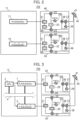
- FIG. 1 A structure of a transmitter according to a first embodiment will be described referring to Fig. 1 .
- a transmitter 101 includes RF circuits 20 and 30, and a controller 11.
- the controller 11 includes a first bit string generator 71 for generating a first bit string, and a second bit string generator 72 for generating a second bit string. Digital outputs from the generators are input to the RF circuits 20 and 30, respectively.
- the digital signal input to the RF circuit 20 is processed by a 2-bit first serial-parallel converter 21 while having an odd bit input to a first multiplier 22.
- the input is multiplied by an output of a first modulation frequency generator 24 so as to be input to a first combiner 26.
- An even bit is input to a second multiplier 23, and multiplied by an output of the modulation frequency generator 24 via a 90-degree phase shifter 25 so as to be further input to the first combiner 26.
- a first mixer 27 up-converts the output of the combiner 26 with an output of a first carrier frequency generation circuit 28, which will be radiated to space by a first antenna 41.
- the digital signal input to the RF circuit 30 is processed by a 2-bit second serial-parallel converter 31 while having an odd bit input to a third multiplier 32.
- the input is multiplied by an output of a second modulation frequency generator 34 so as to be input to a second combiner 36.
- An even bit is input to a fourth multiplier 33, and multiplied by an output of the modulation frequency generator 34 via a second 90-degree phase shifter 35 so as to be further input to the second combiner 36.
- a second mixer 37 up-converts the output of the second combiner 36 with an output of a second carrier frequency generation circuit 38, which will be radiated to air by a second antenna 42 spatially orthogonal to the first antenna 41.
- the first carrier frequency generation circuit 28 is equivalent to the second carrier frequency generation circuit 38.
- the first modulation frequency generation circuit 24 is equivalent to the second modulation frequency generation circuit 34.
- the rotation polarized wave is generated by dividing an output of a bit string generator which is equivalent to the first bit string generator 71 into two branches.
- the branch with one of the polarized wave rotation frequencies is modulated with a cosine wave, and the other is modulated with a sine wave.
- the modulated outputs are up-converted with the carrier frequency, and radiated to air from the two different antennas which are spatially orthogonal to each other.
- the first bit string generator 71 and a second bit string generator 72 generate bit streams having the same odd bits and different (inverted) even bits to be simultaneously (synchronously) output to the RF circuits 20 and 30, respectively.
- the first serial-parallel converter 21 and the second serial-parallel converter 31 allow the first multiplier 22 and the third multiplier 32 to superpose the odd bits of the output from the first bit string generator 71 and the second bit string generator 72 with the cosine wave corresponding to the single cycle of the polarized wave rotation frequency.
- the even bit is superposed with the sine wave corresponding to the single cycle of the polarized wave rotation frequency by the second multiplier 23 and the fourth multiplier 33.
- Outputs of the first multiplier 22 and the second multiplier 23 are synthesized, and up-converted into the carrier frequency by the first mixer 27, which is radiated to air by the first antenna 41.
- Outputs of the third multiplier 32 and the fourth multiplier 33 are synthesized, and up-converted into the carrier frequency by the second mixer 37, which is radiated to air by the second antenna 42.
- each signal before up-conversion is formed as a synthesis of the sine and the cosine waves of the polarized wave rotation frequency.
- Those signals are the same except the code of the sine wave (sin ⁇ p ) which is kept constantly different.
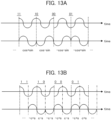
- Outputs of the first combiner 26 and the second combiner 36 are orthogonal to each other with respect to all possible 2-bit combinations as shown in Fig. 13A .
- An upper waveform of Fig. 13A represents the waveform of the cosine wave to be superposed with the odd bit, and a lower waveform represents the waveform of the sine wave to be superposed with the even bit.
- the relationship between those waveforms may be expressed by the following numerical expressions.
- the signals radiated to air from the two antennas which are spatially orthogonal to each other serve to branch the output of the bit string generator equivalent to the first bit string generator 71 into two.
- one of the polarized wave rotation frequency is modulated with the cosine wave, and the other is modulated with the sine wave.
- the modulated outputs are up-converted with the carrier frequency to generate the rotation polarized wave.
- the transmitter 101 includes the first transmission circuit (RF circuit 20) and the second transmission circuit (RF circuit 30) each having at least one common circuit, and the controller 11 configured to generate first digital data (first bit string generated by the first bit string generator 71) so as to be output to the first transmission circuit (RF circuit 20), and to generate second digital data (second bit string generated by the second bit string generator 72) which are different from the first digital data so as to be output to the second transmission circuit (RF circuit 30).
- first digital data first bit string generated by the first bit string generator 71
- second digital data second bit string generated by the second bit string generator 72
- the transmitter transmits the output of the first transmission circuit (RF circuit 20) and the output of the second transmission circuit (RF circuit 30) from the pair of antennas (41, 42) which are spatially orthogonal to each other so as to generate radio wave having the polarized wave rotating orthogonally to the propagation direction.
- the first transmission circuit (RF circuit 20) and the second transmission circuit (RF circuit 30) include the common circuits, for example, the same modulators (21 to 26 in Fig. 1 ), and the same frequency up-converters (27, 28 in Fig. 1 ).
- the controller 11 generates digital data (71, 72 in Fig. 1 ) as second digital data having a part cyclically different from the first digital data.
- the controller 11 generates the digital data (71, 72 in Fig. 1 ) as the second digital data having a part different from the first digital data, and the same part as the first digital data, which are cyclically equivalent with respect to time.
- the controller 11 generates the first digital data and the second digital data (71, 72 in Fig. 1 ) each having the sequential bit string constituted by the coincident bits and the inverted bits alternately and repeatedly arranged in every other bit.
- the controller 11 simultaneously outputs the first digital data and the second digital data to the first transmission circuit (RF circuit 20) and the second transmission circuit (RF circuit 30), respectively.
- the transmitter 101 is configured to input different digital data (71, 72 in Fig. 1 ) to a pair of equivalent transmission circuits (20, 30 in Fig. 1 ) provided with the modulators (21 to 26 in Fig. 1 ), and the frequency up-converters (27, 28 in Fig. 1 ), transmit outputs of the respective transmission circuits from the pair of antennas (41, 42 in Fig. 1 ) which are spatially orthogonal to each other, and generate the radio wave having the polarized wave rotating orthogonally to the propagation direction.
- the modulator (21 to 26 in Fig. 1 ) executes QPSK modulation (see Fig. 13A ), or offset QPSK modulation (see Fig. 13B ).
- a pair of commercial RF chips or wireless modules for the general wireless system using QPSK modulation are employed to simultaneously input different bit strings to the respective modules from the commercial controller so that the rotation polarized wave is radiated. This makes it possible to provide the transmitter of the rotation polarized wave at lower costs.
- a structure of a transmitter according to a second embodiment will be described referring to Fig. 2 .
- a transmitter 102 includes RF circuits 40 and 50, and the controller 11.
- a first half-bit phase delay unit 29 is inserted between the first serial-parallel converter 21 and the second multiplier 23
- a second half-bit phase delay unit 39 is inserted between the second serial-parallel converter 31 and the fourth multiplier 33.
- Those half-bit phase delay units allow the RF circuits 40 and 50 to execute the offset QPSK modulation.
- the operation according to the embodiment as shown in Fig. 2 is different from the one as shown in Fig. 13A . That is, the cosine wave to be superposed with the odd bit is shifted from the sine wave to be superposed with the even bit by half cycle. However, this clearly shows that the cosine wave and the sine wave are orthogonal to each other by each half-cycle of the polarized wave rotation. Therefore, outputs of the combiners 26 and 36 of the respective RF circuits 40 and 50 are orthogonal to each other on the entire time axis analogous to the relationship as indicated by the numerical expression 1 or 2.
- the second embodiment employs a pair of commercial RF chips or wireless modules used for the generally employed wireless system using the offset QPSK modulation. Simultaneous input of different bit strings to the respective modules from the commercial controller allows radiation of the rotation polarized wave. As a result, the transmitter of the rotation polarized wave may be put to practical use at low costs.
- a structure of a transmitter according to a third embodiment will be described referring to Fig. 3 .
- the transmitter according to the third embodiment is different from the transmitter according to the first embodiment as shown in Fig. 1 in a controller 13, instead of the controller 11, which is provided with a CPU 3 and a data bus 4.
- the other structure is substantially the same as that of the transmitter according to the first embodiment as shown in Fig. 1 , and explanation thereof, thus will be omitted.
- the CPU 3 sequentially generates the bit strings similar to those generated by the first bit string generator 71 and the second bit string generator 72, and accumulates the bit strings in a first bit string buffer 1 and a second bit string buffer 2, respectively via the data bus 4.
- the CPU 3 After completion of accumulating the data in both the bit string buffers, the CPU 3 issues a command to simultaneously input contents of the first bit string buffer 1 and the second bit string buffer 2 to the RF circuits 20 and 30, respectively.
- the third embodiment allows the CPU to generate a pair of digital data for generation of the rotation polarized wave, and control the timing for transmitting both the digital data to the RF circuits, respectively. This makes it possible to adjust the timing for transmitting the bit strings to be input to the pair of RF circuits, respectively.
- a structure of a transmitter according to a fourth embodiment will be described referring to Fig. 4 .
- the transmitter according to the fourth embodiment is different from the transmitter according to the third embodiment as shown in Fig. 3 in a controller 14, instead of the controller 13, which is provided with a third bit string buffer 5, a fourth bit string buffer 6, a first selector 7, and a second selector 8.
- the other structure is substantially the same as that of the transmitter according to the third embodiment as shown in Fig. 3 , and explanation thereof, thus will be omitted.
- the next bit string to be accumulated in the first bit string buffer 1 is accumulated in the third bit string buffer 5, and the next bit string to be accumulated in the second bit string buffer 2 is accumulated in the fourth bit string buffer 6 by the CPU 3 via the data bus 4.
- the first selector 7 switches between the first bit string buffer 1 and the third bit string buffer 5.
- the second selector 8 switches between the second bit string buffer 2 and the fourth bit string buffer 6.
- the CPU 3 controls the selectors 7 and 8.
- the digital data to be input to the RF circuit 20 and the RF circuit 30 may be accumulated in the bit string buffers simultaneously with output of those data from the bit string buffer. It is effective for improving the rate of transmitting the information to be transmitted by the transmitter.
- a structure of a transmitter according to a fifth embodiment will be described referring to Fig. 5 .
- the transmitter according to the fifth embodiment is different from the transmitter according to the first embodiment as shown in Fig. 1 in a controller 15, instead of the controller 11, which is provided with a clock generation circuit 75, a 1/2 decimeter 76, a first delay circuit 77, a second delay circuit 78, a selector switch 74, and an inverter 73.
- the other structure is substantially the same as that of the transmitter according to the first embodiment as shown in Fig. 1 , and explanation thereof, thus will be omitted.
- An output of the first bit string generator 71 is branched into three.
- the first branch is output to the RF circuit 20 via the first delay circuit 77.
- the second branch is output to the selector switch 74 via the second delay circuit 78.
- the third branch is further output to the selector switch 74 via the inverter 73.
- An output of the clock generation circuit 75 is decimated to two clocks so that the output of the selector switch 74 is switched between the direct output and the inverted output of the first bit string generator 71 for each bit.
- a delay amount of the delay circuit 77 is preliminarily determined so that the digital data are simultaneously input to the RF circuits 20 and 30, respectively.
- a delay amount of the delay circuit 78 is preliminarily adjusted so that the direct input and the inverted input to the selector switch 74 is alternately output continuously.
- the number of the bit string generators may be reduced, it is effective for reducing the memory size of the transmitter for generating the rotation polarized wave. This makes it possible to reduce the transmitter size as well as the cost.
- a structure of a transmitter according to a sixth embodiment will be described referring to Figs. 6A and 6B .
- the transmitter according to the sixth embodiment is different from the transmitter according to the third embodiment as shown in Fig. 3 in a controller 16, instead of the controller 13, which is provided with a counter 51, a unit bit string buffer 52, an interpolator 53, a first code multiplier 54, a second code multiplier 55, a code selector switch 56, a code table 57, a first diffusion bit string buffer 58, and a second diffusion bit string buffer 59.
- the other structure is substantially the same as that of the transmitter according to the third embodiment as shown in Fig. 3 , and explanation thereof, thus will be omitted.
- the CPU 3 generates information bit strings, and sequentially accumulates the data in the first bit string buffer 1.
- a predetermined number of units of the accumulated bit strings are accumulated in the unit bit string buffer 52 via the counter 51 under the control of the CPU 3 using the value of the counter 51.
- the bit strings accumulated in the unit bit string buffer 52 are reproduced for each bit by the interpolator 53.
- Fig. 6B represents extension of the bit string length by four times through reproduction of four bits b a and four bits b b by interpolation.
- the pair of bit strings longer than the unit bit, which have been preliminarily stored in the code table 57 are multiplied using the first code multiplier 54 and the second code multiplier 55.
- the resultant data are accumulated in the first diffusion bit string buffer 58, and the second diffusion bit string buffer 59.
- one bit of the extended bit string is allocated to 2-bit code taken from the code table 57.
- the code table 57 contains a pair of code strings having the odd bit and the inverted even bit.
- the bit string with the extended information is superposed with the bit string stored in the code table 57 so that the signal diffused with the pair of code strings is accumulated in the first diffusion bit string buffer 58 and the second diffusion bit string buffer 59.
- the information is diffused as described above.
- the bit strings to be accumulated in the first diffusion bit string buffer 58 and the second diffusion bit string buffer 59 are selected so that the odd bits are the same, and the even bits are inverted.
- the selected data are preliminarily stored in the code table 57.
- the CPU 3 refers to the unit bit strings accumulated in the unit bit string buffer 52 to select the bit string from the code table 57 by controlling the code selector switch 56.
- the bit strings accumulated in the first diffusion bit string buffer 58 and the second diffusion bit string buffer 59 are simultaneously input to the RF circuits 20 and 30, respectively. Accordingly, the rotation polarized wave is radiated through the operation similar to the one as described in the embodiment referring to Fig. 3 .
- the information signal is diffused with the code having the bit length loner than the original bit length. It is therefore effective for security of information transmission by concealing the information signal.
- a structure of a transmitter according to a seventh embodiment will be described referring to Fig. 7 .
- the transmitter according to the seventh embodiment is different from the transmitter according to the embodiment as shown in Fig. 6 in a controller 17, instead of the controller 16, which is provided with a second bit string buffer 60, a second counter 61, a second unit bit string buffer 62, a second interpolator 63, a delay circuit 64, and a second code selector switch 66, and a first code selector switch 156.
- the other structure is substantially the same as that of the transmitter according to the sixth embodiment, and explanation thereof, thus will be omitted.
- the CPU 3 generates two different types of information bit strings, and sequentially accumulates the data in the first bit string buffer 1 and the second bit string buffer 60.
- An operation which relates to the bit strings accumulated in the first bit string buffer 1 is similar to the operation as described in the embodiment as shown in Fig. 6 except the single output from the first code selector switch 156.
- a predetermined number of units of the bit strings accumulated in the second bit string buffer 60 are accumulated in the second unit bit string buffer 62 via the second counter 61 under the control of the CPU 3 using the value of the second counter 61.
- Each single bit of the bit strings accumulated in the second unit bit string buffer 62 is reproduced by the second interpolator 63, and multiplied by the pair of bit strings which are longer than the unit bit string preliminarily stored in the code table 57 using the second code multiplier 55.
- the resultant data are accumulated in the second diffusion bit string buffer 59.
- the respective bit strings to be accumulated in the first diffusion bit string buffer 58 and the second diffusion bit string buffer 59 are selected so that the odd bits are the same, and the even bits are inverted.
- the data are preliminarily stored in the code table 57.
- the CPU 3 refers to the unit bit strings accumulated in the unit bit string buffer 52 to select the data from the code table 57 by controlling the first code selector switch 156 and the second code selector switch 66.
- a delay amount of the delay circuit 64 is preliminarily adjusted so that the bit strings accumulated in the first diffusion bit string buffer 58 and the second diffusion bit string buffer 59 are simultaneously input to the RF circuits 20 and 30, respectively. Then the rotation polarized wave is radiated through the operation similar to the one as described in the embodiment referring to FIG. 3 .
- the information bits to be input to the RF circuits 20 and 30 are obtained through diffusion with codes.
- the bit strings are generated to have the same odd bits, and the inverted even bits in the same sequence in two systems independent from each other.
- the digitally controllable delay circuit is inserted into one of the two signal lines to be input to the two RF circuits. As a result, it is possible to synchronize input of the signals to the two RF circuits.
- the seventh embodiment it is possible not only to improve generation accuracy of the rotation polarized wave but also simplify the operation of the code selector switch compared with the embodiment as shown in Fig. 6 . It is therefore effective for simplifying the CPU control and reducing power consumed by the transmitter.
- a structure of a transmitter according to an eighth embodiment will be described referring to Fig. 8 .
- the transmitter according to the eighth embodiment is different from the transmitter according to the seventh embodiment as shown in Fig. 7 in a controller 18, instead of the controller 17, which is provided with a first register 65, a second register 67, and the data bus 4.
- the other structure is substantially the same as that of the transmitter according to the seventh embodiment, and explanation thereof, thus will be omitted.
- outputs of the first code multiplier 54 and the second code multiplier 55 are accumulated in the first register 65 and the second register 67, respectively.
- the data accumulated in the first register 65 and the second register 67 are accumulated in the first diffusion bit string buffer 58 and the second diffusion bit string buffer 59, respectively via the data bus 4 so that the accumulated data are output to the RF circuits 20 and 30, respectively under the control of the CPU 3.
- a structure of a transmitter according to a ninth embodiment will be described referring to Fig. 9 .
- the transmitter according to the ninth embodiment is different from the transmitter according to the eighth embodiment as shown in Fig. 8 in a controller 19, instead of the controller 18, which is provided with a third diffusion bit string buffer 68, a fourth diffusion bit string buffer 69, a first selector 88, and a second selector 89.
- the other structure is substantially the same as that of the transmitter according to the eighth embodiment, and explanation thereof, thus will be omitted.
- the CPU 3 accumulates the next bit string to be accumulated in the first diffusion bit string buffer 58 in the third diffusion bit string buffer 68 via the data bus 4, and the next bit string to be accumulated in the second diffusion bit string buffer 59 in the fourth diffusion bit string buffer 69 via the data bus 4.
- the first selector 88 switches between the first diffusion bit string buffer 58 and the third diffusion bit string buffer 68.
- the second selector 89 switches between the second diffusion bit string buffer 59 and the fourth diffusion bit string buffer 69.
- the CPU 3 controls the selectors 88 and 89.
- the ninth embodiment it is possible to accumulate the digital data to be input to the RF circuits 20 and 30, respectively in the bit string buffers simultaneously with output of those data from the bit string buffers. It is effective for improving the rate for transmitting the information to be transmitted by the transmitter.
- a structure of a receiver constituting a wireless device according to a tenth embodiment will be described referring to Fig. 10 .
- a receiver 200 which receives the rotation polarized wave from the transmitter for generating the rotation polarized wave includes receiving antennas 43 and 44 which are spatially orthogonal to each other, RF circuit elements, and a baseband circuit 90. Signals input from the first receiving antenna 43 and the second receiving antenna 44 are down-converted into a rotation polarized wave signal with the output of a carrier local generation circuit 81 at the same frequency as the carrier frequency of the transmitter through a first receiving mixer 82 and a second receiving mixer 83.
- Outputs from a rotation polarized wave frequency cosine wave generation circuit 84 and a rotation polarized wave frequency sine wave generation circuit 85 are multiplied using a first receiving multiplier circuit 86 and a second receiving multiplier circuit 87, and converted into a baseband signal band.
- the data are sequentially delayed by a first delay unit group 91 and a second delay unit group 92 each constituted by multiple delay units.
- the multiple data are input to a baseband signal processing circuit 99.
- the receiver according to the tenth embodiment is capable of inputting values corresponding to components of the cosine wave and the sine wave of the rotation polarized wave at the respective timings derived from dividing the single cycle of the rotation polarized wave to the baseband signal processing circuit. This allows the use of the two antennas 43 and 44 spatially orthogonal to each other so as to demodulate the reception signal with respect to the angular components of all polarized waves orthogonal to the advancing direction of the incoming wave.
- An elevator monitoring control system 1100 is configured to move multiple cars 1111 up and down in a building 1101 where the elevator is installed.
- Combinations of a base station rotation polarized wave wireless device 1103 and a base station 2-orthogonal polarized wave integrated antenna 1102 are disposed on the floor and the ceiling inside the building 1101.
- Terminal station 2-orthogonal polarized wave integrated antennas 1112 are disposed on an outer ceiling and an outer floor surface of the car 1111, and linked to a wireless terminal 1113 via a high frequency cable 1114.
- the inside of the building 1101 serves as a wireless transmission medium for the base station rotation polarized wave wireless device 1103 and the wireless terminal 1113.
- the polarized wave differs at a timing when the electromagnetic wave transmitted from multiple wireless terminals 1113 reaches the base station rotation polarized wave wireless unit 1103.
- the car will change its relative position.
- the polarized wave of the electromagnetic wave that reaches the base station rotation polarized wave wireless device 1103 from the multiple wireless terminals 1113 generally fluctuates.
- the processing for a wireless channel measurement mode and a data transmission mode is executed. This makes it possible to achieve highly reliable wireless communication between the elevator and the fixed rotation polarized wave wireless device in the elevator system having difficulties in predicting the relative fixed position.
- the elevator may be remotely controlled and monitored without using the wired connection means in the building 1101. It is therefore possible to eliminate the wired connection means such as cables, and achieve the equivalent transportation capacity in the building with smaller volume.
- the transportation capacity may be improved by increasing the dimension of the elevator in the building with the equivalent volume.
- the information inside the car 1111 may be sent to the outside by means of the compact and light-weight transmitter with low power consumption, it is possible to reduce the weight of the communication apparatus for information transmission in the car. It is effective not only for saving power consumed by the elevator system but also for reducing maintenance costs for the communication apparatus.
- a substation facility monitoring control system 1200 includes multiple transformers 1201 each having a combination of a wireless terminal 1203 and a wireless terminal 2-orthogonal polarized wave integrated antenna 1202.
- a wireless base station 1211 is established near the multiple transformers 1201, and includes a combination of a rotation polarized wave wireless device 1213 for transmitting and receiving the rotation polarized wave according to the present invention, and a rotation polarized wave 2-orthogonal polarized wave integrated antenna 1212.
- the transformer is an extremely large with its size in the order of several meters compared with the wavelength which covers the electromagnetic wave frequency of the wireless device in the range from several hundreds of MHz to several GHz.
- the electromagnetic waves receive multiple reflections from the respective transformers 1201 to form a multiwave interference environment. Then the wave transmitted from the wireless terminals 1203 each fixed in the respective transformers 1201 reaches the rotation polarized wave wireless device 1213 installed in the wireless terminal station 1211 while exhibiting the different polarized waves.
- the twelfth embodiment achieves highly reliable wireless communication between the rotation polarized wave wireless device 1213 and the multiple wireless terminals 1203. This makes it possible to remotely control and monitor the transformers 1201 by means of the wireless connection means using the wireless device through the multiple wireless base stations 1211 without using the wired connection means.
- the problem of high-pressure dielectric power caused by the use of the wired connection means such as the cable may be solved, which makes it possible to reduce the cable laying cost. It is effective for safety improvement and cost reduction of the system for controlling and monitoring the transformers 1201. Furthermore, it is possible to reduce the cost of the wireless devices to be installed in a large number of transformers 1201. This makes it possible to reduce the cost for introducing the system that wirelessly controls the substation facility monitoring control system 1200.
Landscapes
- Engineering & Computer Science (AREA)
- Computer Networks & Wireless Communication (AREA)
- Signal Processing (AREA)
- Transmitters (AREA)
- Radio Transmission System (AREA)
Claims (11)
- Transmetteur (101), comprenant :un premier circuit de transmission (20) et un second circuit de transmission (30) présentant au moins un circuit commun ; etun dispositif de commande (11) qui génère des premières données numériques (71), une pluralité de premiers bits étant agencés séquentiellement dans les premières données numériques (71), et délivre en sortie les premières données numériques au premier circuit de transmission (20), et génère des secondes données numériques (72) différentes des premières données numériques, une pluralité de seconds bits étant agencés séquentiellement dans les secondes données numériques (72), et délivre en sortie les secondes données numériques au second circuit de transmission (30), dans lequel des sorties du premier circuit de transmission (20) et du second circuit de transmission (30) sont transmises à partir d'une paire d'antennes (41, 42) spatialement orthogonales l'une par rapport à l'autre pour générer une onde radio présentant une onde polarisée tournant orthogonalement à une direction de propagation,caractérisé en ce que le dispositif de commande (11) génère en outre des données numériques en tant que secondes données numériques, présentant une partie cycliquement différente des premières données numériques,dans lequel les premières données numériques (71) et les secondes données numériques (72) fournissent des flux de bits présentant les mêmes bits impairs et des bits pairs inversés pour être délivrés en sortie simultanément vers le premier circuit de transmission (20) et le second circuit de transmission (30), respectivement.
- Transmetteur selon la revendication 1, dans lequel le premier circuit d'émission (20) et le second circuit d'émission (30) incluent chacun les mêmes modulateurs (24, 34) et les mêmes convertisseurs élévateurs de fréquence (27, 37) que le circuit commun.
- Transmetteur selon la revendication 1, dans lequel :le dispositif de commande (13) stocke les premières données numériques et les secondes données numériques dans une paire de tampons de signal (1, 2) formés dans un circuit numérique incluant un circuit de traitement de signal ; etle dispositif de commande délivre en sortie les données numériques simultanément vers le premier circuit de transmission et le second circuit de transmission, respectivement sous la commande du circuit de traitement de signal.
- Transmetteur selon la revendication 3, dans lequel :le circuit numérique incluant le circuit de traitement de signal forme une paire de groupes de tampons de signal (1, 5 ; 2, 6) incluant une pluralité de tampons de signal (1, 2, 5, 6) ; etle circuit numérique exécute une opération de délivrance en sortie des données numériques à partir d'un tampon (1, 2, 5, 6) parmi les groupes de tampons de signal (1, 5 ; 2, 6) simultanément avec une opération d'accumulation des données numériques dans un autre tampon (1, 2, 5, 6) sous la commande du circuit de traitement de signal.
- Transmetteur selon la revendication 1, dans lequel le dispositif de commande (11) délivre en sortie les données numériques dérivées de la diffusion d'un signal d'information avec deux codes cycliquement et partiellement différents en tant que premières données numériques et secondes données numériques au premier circuit de transmission et au second circuit de transmission, respectivement.
- Transmetteur selon la revendication 5, dans lequel le dispositif de commande (11) divise des chaînes de bits séquentielles incluant le signal d'information en groupes de bits unitaires chacun avec un nombre fixe de bits, et délivre en sortie une paire de signaux différents dérivés de la diffusion des groupes de bits unitaires avec une paire de codes partiellement différente vers le premier circuit de transmission et le second circuit de transmission en tant que premières données numériques et secondes données numériques, respectivement.
- Transmetteur selon la revendication 1, dans lequel :le dispositif de commande (11) divise chacune d'une paire de chaînes de bits séquentielles incluant un signal d'information en groupes de bits unitaires présentant chacun un nombre de bits fixe ; etle dispositif de commande (11) délivre en sortie une paire de signaux différents dérivés de la diffusion des groupes de bits unitaires respectifs avec une paire de codes partiellement différents au premier circuit de transmission (20) et au second circuit de transmission (30) en tant que premières données numériques et secondes données numériques, respectivement, via un circuit de retard (64).
- Transmetteur selon la revendication 2, dans lequel le modulateur (24, 34) exécute une modulation QPSK ou une modulation QPSK décalée.
- Dispositif sans fil, comprenant :le transmetteur (101) selon la revendication 1 ; etun récepteur (200) qui reçoit des signaux de bande de base à deux lignes dérivés de la multiplication de signaux convertis vers le bas reçus d'une paire d'antennes (43, 44) spatialement orthogonales l'une par rapport à l'autre par une onde cosinusoïdale et une onde sinusoïdale d'une fréquence de rotation d'onde polarisée, respectivement.
- Système de commande de surveillance d'ascenseur (1100) configuré pour surveiller et commander à distance un ascenseur (1111) à partir d'un bâtiment (1101) comprenant le dispositif sans fil (101, 200) selon la revendication 9.
- Système de commande de surveillance d'installation de sous-station (1200) configuré pour surveiller et commander à distance une sous-station à partir d'une station de base sans fil comprenant le dispositif sans fil (101, 200) selon la revendication 9.
Applications Claiming Priority (1)
| Application Number | Priority Date | Filing Date | Title |
|---|---|---|---|
| JP2018154458A JP7139188B2 (ja) | 2018-08-21 | 2018-08-21 | 送信機 |
Publications (2)
| Publication Number | Publication Date |
|---|---|
| EP3614574A1 EP3614574A1 (fr) | 2020-02-26 |
| EP3614574B1 true EP3614574B1 (fr) | 2023-12-06 |
Family
ID=67437969
Family Applications (1)
| Application Number | Title | Priority Date | Filing Date |
|---|---|---|---|
| EP19186969.2A Active EP3614574B1 (fr) | 2018-08-21 | 2019-07-18 | Transmetteur générant une onde polarisée rotative |
Country Status (3)
| Country | Link |
|---|---|
| US (1) | US11081811B2 (fr) |
| EP (1) | EP3614574B1 (fr) |
| JP (1) | JP7139188B2 (fr) |
Families Citing this family (1)
| Publication number | Priority date | Publication date | Assignee | Title |
|---|---|---|---|---|
| DE102020117335B4 (de) * | 2020-07-01 | 2022-01-13 | Audi Aktiengesellschaft | Betreiben einer Kommunikationseinrichtung eines Kraftfahrzeugs |
Family Cites Families (8)
| Publication number | Priority date | Publication date | Assignee | Title |
|---|---|---|---|---|
| JP2003046486A (ja) * | 2001-07-27 | 2003-02-14 | Oki Electric Ind Co Ltd | 符号化回路 |
| JP4643462B2 (ja) * | 2006-02-08 | 2011-03-02 | 株式会社東芝 | 無線機及び偏波切替方法 |
| PL216976B1 (pl) | 2009-08-25 | 2014-06-30 | Michał Głogowski | Wielostopniowy pneumatyczny tłok kompensacyjny |
| JP5632530B2 (ja) | 2011-03-09 | 2014-11-26 | 株式会社日立製作所 | 偏波角度分割ダイバシチ無線送信機、無線受信機、および無線通信システム |
| WO2016075785A1 (fr) * | 2014-11-13 | 2016-05-19 | 株式会社日立製作所 | Système de communication sans fil, et système l'utilisant |
| JP6228108B2 (ja) * | 2014-12-18 | 2017-11-08 | 株式会社日立製作所 | 無線通信システム |
| JP6581437B2 (ja) * | 2015-08-25 | 2019-09-25 | 株式会社日立製作所 | 無線通信システム |
| CN108028695B (zh) * | 2016-05-10 | 2021-01-15 | 株式会社日立制作所 | 发送机以及接收机 |
-
2018
- 2018-08-21 JP JP2018154458A patent/JP7139188B2/ja active Active
-
2019
- 2019-07-18 EP EP19186969.2A patent/EP3614574B1/fr active Active
- 2019-08-02 US US16/530,307 patent/US11081811B2/en active Active
Non-Patent Citations (1)
| Title |
|---|
| ROHANI K: "Open-loop transmit diversity for CDMA forward link", EMERGING TECHNOLOGIES SYMPOSIUM: BROADBAND, WIRELESS INTERNET ACCESS, 2000 IEEE APRIL 10-11, 2000, PISCATAWAY, NJ, USA,IEEE, 10 April 2000 (2000-04-10), pages 5pp, XP032403606, ISBN: 978-0-7803-6364-9, DOI: 10.1109/ETS.2000.916512 * |
Also Published As
| Publication number | Publication date |
|---|---|
| US20200067204A1 (en) | 2020-02-27 |
| US11081811B2 (en) | 2021-08-03 |
| JP2020031295A (ja) | 2020-02-27 |
| EP3614574A1 (fr) | 2020-02-26 |
| JP7139188B2 (ja) | 2022-09-20 |
Similar Documents
| Publication | Publication Date | Title |
|---|---|---|
| EP0655179B1 (fr) | Methode de test d'un emetteur-recepteur et station de base de systeme de radiocommunications a repartition dans le temps | |
| EP2572457B1 (fr) | Limitation de la consommation de puissance dans un système de communication sans fil et mise en place d'une couverture radio directionnelle adaptée | |
| US5710977A (en) | Apparatus for measuring multipath propagation characteristics | |
| FI112567B (fi) | Radiolinkkijärjestelmän terminaalien synkronointi | |
| AU674466B2 (en) | A method for minimizing a phase error of a transmitter | |
| CA2406756A1 (fr) | Couverture radiofrequence amelioree d'une region fermee a l'aide d'un arrangement d'emetteurs-recepteurs situes dans cette region | |
| EP3614574B1 (fr) | Transmetteur générant une onde polarisée rotative | |
| EP1705843A1 (fr) | Procédé et dispositif pour augmenter la capacité d'un systhème MIMO (multiple-input-multiple-output) utilisant des relais | |
| US10749273B2 (en) | Wireless communication system and wireless surveillance control system | |
| US20090067383A1 (en) | Method and apparatus for a frequency division duplex communication using a time division duplex modem | |
| KR100740396B1 (ko) | 도로측 협대역 무선 통신 장치 | |
| US10148338B1 (en) | Wireless communication system | |
| JP2014132726A (ja) | 無線通信システム | |
| JP2002300097A (ja) | 基地局、移動局および移動通信システム | |
| KR20170025339A (ko) | 기지국 급전선 공유 장치 및 방법, 그리고 이를 이용한 기지국 장치 | |
| CN111313928B (zh) | 支持多种制式的超宽带收发机架构及相应的无线门禁装置 | |
| KR101037835B1 (ko) | 마이크로웨이브 링크를 이용하여 다수의 섹터를 서비스하기위한 마이크로웨이브 중계기 | |
| JP3048930B2 (ja) | ディジタルコードレス電話装置 | |
| WO2016013143A1 (fr) | Dispositif de transmission sans fil et procédé de transmission sans fil | |
| SU902273A1 (ru) | Ретрансл тор системы св зи | |
| KR100617536B1 (ko) | 무선가입자망 단말기의 주파수 제어 장치 | |
| JP2005057594A (ja) | 伝送方法および伝送装置 | |
| JPH06268622A (ja) | 集中基地局の通信装置 | |
| JP2006042202A (ja) | 通信装置、発振信号周波数変更方法及びプログラム | |
| CN109995395A (zh) | 一种射频收发机 |
Legal Events
| Date | Code | Title | Description |
|---|---|---|---|
| PUAI | Public reference made under article 153(3) epc to a published international application that has entered the european phase |
Free format text: ORIGINAL CODE: 0009012 |
|
| STAA | Information on the status of an ep patent application or granted ep patent |
Free format text: STATUS: REQUEST FOR EXAMINATION WAS MADE |
|
| 17P | Request for examination filed |
Effective date: 20190718 |
|
| AK | Designated contracting states |
Kind code of ref document: A1 Designated state(s): AL AT BE BG CH CY CZ DE DK EE ES FI FR GB GR HR HU IE IS IT LI LT LU LV MC MK MT NL NO PL PT RO RS SE SI SK SM TR |
|
| AX | Request for extension of the european patent |
Extension state: BA ME |
|
| STAA | Information on the status of an ep patent application or granted ep patent |
Free format text: STATUS: EXAMINATION IS IN PROGRESS |
|
| 17Q | First examination report despatched |
Effective date: 20201013 |
|
| GRAP | Despatch of communication of intention to grant a patent |
Free format text: ORIGINAL CODE: EPIDOSNIGR1 |
|
| STAA | Information on the status of an ep patent application or granted ep patent |
Free format text: STATUS: GRANT OF PATENT IS INTENDED |
|
| INTG | Intention to grant announced |
Effective date: 20230623 |
|
| GRAS | Grant fee paid |
Free format text: ORIGINAL CODE: EPIDOSNIGR3 |
|
| GRAA | (expected) grant |
Free format text: ORIGINAL CODE: 0009210 |
|
| STAA | Information on the status of an ep patent application or granted ep patent |
Free format text: STATUS: THE PATENT HAS BEEN GRANTED |
|
| AK | Designated contracting states |
Kind code of ref document: B1 Designated state(s): AL AT BE BG CH CY CZ DE DK EE ES FI FR GB GR HR HU IE IS IT LI LT LU LV MC MK MT NL NO PL PT RO RS SE SI SK SM TR |
|
| REG | Reference to a national code |
Ref country code: GB Ref legal event code: FG4D |
|
| REG | Reference to a national code |
Ref country code: DE Ref legal event code: R096 Ref document number: 602019042683 Country of ref document: DE |
|
| REG | Reference to a national code |
Ref country code: CH Ref legal event code: EP |
|
| REG | Reference to a national code |
Ref country code: IE Ref legal event code: FG4D |
|
| REG | Reference to a national code |
Ref country code: LT Ref legal event code: MG9D |
|
| PG25 | Lapsed in a contracting state [announced via postgrant information from national office to epo] |
Ref country code: GR Free format text: LAPSE BECAUSE OF FAILURE TO SUBMIT A TRANSLATION OF THE DESCRIPTION OR TO PAY THE FEE WITHIN THE PRESCRIBED TIME-LIMIT Effective date: 20240307 |
|
| REG | Reference to a national code |
Ref country code: NL Ref legal event code: MP Effective date: 20231206 |
|
| PG25 | Lapsed in a contracting state [announced via postgrant information from national office to epo] |
Ref country code: LT Free format text: LAPSE BECAUSE OF FAILURE TO SUBMIT A TRANSLATION OF THE DESCRIPTION OR TO PAY THE FEE WITHIN THE PRESCRIBED TIME-LIMIT Effective date: 20231206 |
|
| PG25 | Lapsed in a contracting state [announced via postgrant information from national office to epo] |
Ref country code: ES Free format text: LAPSE BECAUSE OF FAILURE TO SUBMIT A TRANSLATION OF THE DESCRIPTION OR TO PAY THE FEE WITHIN THE PRESCRIBED TIME-LIMIT Effective date: 20231206 |
|
| PG25 | Lapsed in a contracting state [announced via postgrant information from national office to epo] |
Ref country code: LT Free format text: LAPSE BECAUSE OF FAILURE TO SUBMIT A TRANSLATION OF THE DESCRIPTION OR TO PAY THE FEE WITHIN THE PRESCRIBED TIME-LIMIT Effective date: 20231206 Ref country code: GR Free format text: LAPSE BECAUSE OF FAILURE TO SUBMIT A TRANSLATION OF THE DESCRIPTION OR TO PAY THE FEE WITHIN THE PRESCRIBED TIME-LIMIT Effective date: 20240307 Ref country code: ES Free format text: LAPSE BECAUSE OF FAILURE TO SUBMIT A TRANSLATION OF THE DESCRIPTION OR TO PAY THE FEE WITHIN THE PRESCRIBED TIME-LIMIT Effective date: 20231206 Ref country code: BG Free format text: LAPSE BECAUSE OF FAILURE TO SUBMIT A TRANSLATION OF THE DESCRIPTION OR TO PAY THE FEE WITHIN THE PRESCRIBED TIME-LIMIT Effective date: 20240306 |
|
| REG | Reference to a national code |
Ref country code: AT Ref legal event code: MK05 Ref document number: 1639369 Country of ref document: AT Kind code of ref document: T Effective date: 20231206 |
|
| PG25 | Lapsed in a contracting state [announced via postgrant information from national office to epo] |
Ref country code: NL Free format text: LAPSE BECAUSE OF FAILURE TO SUBMIT A TRANSLATION OF THE DESCRIPTION OR TO PAY THE FEE WITHIN THE PRESCRIBED TIME-LIMIT Effective date: 20231206 |
|
| PG25 | Lapsed in a contracting state [announced via postgrant information from national office to epo] |
Ref country code: SE Free format text: LAPSE BECAUSE OF FAILURE TO SUBMIT A TRANSLATION OF THE DESCRIPTION OR TO PAY THE FEE WITHIN THE PRESCRIBED TIME-LIMIT Effective date: 20231206 Ref country code: RS Free format text: LAPSE BECAUSE OF FAILURE TO SUBMIT A TRANSLATION OF THE DESCRIPTION OR TO PAY THE FEE WITHIN THE PRESCRIBED TIME-LIMIT Effective date: 20231206 Ref country code: NO Free format text: LAPSE BECAUSE OF FAILURE TO SUBMIT A TRANSLATION OF THE DESCRIPTION OR TO PAY THE FEE WITHIN THE PRESCRIBED TIME-LIMIT Effective date: 20240306 Ref country code: NL Free format text: LAPSE BECAUSE OF FAILURE TO SUBMIT A TRANSLATION OF THE DESCRIPTION OR TO PAY THE FEE WITHIN THE PRESCRIBED TIME-LIMIT Effective date: 20231206 Ref country code: LV Free format text: LAPSE BECAUSE OF FAILURE TO SUBMIT A TRANSLATION OF THE DESCRIPTION OR TO PAY THE FEE WITHIN THE PRESCRIBED TIME-LIMIT Effective date: 20231206 Ref country code: HR Free format text: LAPSE BECAUSE OF FAILURE TO SUBMIT A TRANSLATION OF THE DESCRIPTION OR TO PAY THE FEE WITHIN THE PRESCRIBED TIME-LIMIT Effective date: 20231206 |
|
| PG25 | Lapsed in a contracting state [announced via postgrant information from national office to epo] |
Ref country code: IS Free format text: LAPSE BECAUSE OF FAILURE TO SUBMIT A TRANSLATION OF THE DESCRIPTION OR TO PAY THE FEE WITHIN THE PRESCRIBED TIME-LIMIT Effective date: 20240406 |
|
| PG25 | Lapsed in a contracting state [announced via postgrant information from national office to epo] |
Ref country code: AT Free format text: LAPSE BECAUSE OF FAILURE TO SUBMIT A TRANSLATION OF THE DESCRIPTION OR TO PAY THE FEE WITHIN THE PRESCRIBED TIME-LIMIT Effective date: 20231206 Ref country code: CZ Free format text: LAPSE BECAUSE OF FAILURE TO SUBMIT A TRANSLATION OF THE DESCRIPTION OR TO PAY THE FEE WITHIN THE PRESCRIBED TIME-LIMIT Effective date: 20231206 |
|
| PG25 | Lapsed in a contracting state [announced via postgrant information from national office to epo] |
Ref country code: SK Free format text: LAPSE BECAUSE OF FAILURE TO SUBMIT A TRANSLATION OF THE DESCRIPTION OR TO PAY THE FEE WITHIN THE PRESCRIBED TIME-LIMIT Effective date: 20231206 |
|
| PG25 | Lapsed in a contracting state [announced via postgrant information from national office to epo] |
Ref country code: SM Free format text: LAPSE BECAUSE OF FAILURE TO SUBMIT A TRANSLATION OF THE DESCRIPTION OR TO PAY THE FEE WITHIN THE PRESCRIBED TIME-LIMIT Effective date: 20231206 Ref country code: SK Free format text: LAPSE BECAUSE OF FAILURE TO SUBMIT A TRANSLATION OF THE DESCRIPTION OR TO PAY THE FEE WITHIN THE PRESCRIBED TIME-LIMIT Effective date: 20231206 Ref country code: RO Free format text: LAPSE BECAUSE OF FAILURE TO SUBMIT A TRANSLATION OF THE DESCRIPTION OR TO PAY THE FEE WITHIN THE PRESCRIBED TIME-LIMIT Effective date: 20231206 Ref country code: IT Free format text: LAPSE BECAUSE OF FAILURE TO SUBMIT A TRANSLATION OF THE DESCRIPTION OR TO PAY THE FEE WITHIN THE PRESCRIBED TIME-LIMIT Effective date: 20231206 Ref country code: IS Free format text: LAPSE BECAUSE OF FAILURE TO SUBMIT A TRANSLATION OF THE DESCRIPTION OR TO PAY THE FEE WITHIN THE PRESCRIBED TIME-LIMIT Effective date: 20240406 Ref country code: EE Free format text: LAPSE BECAUSE OF FAILURE TO SUBMIT A TRANSLATION OF THE DESCRIPTION OR TO PAY THE FEE WITHIN THE PRESCRIBED TIME-LIMIT Effective date: 20231206 Ref country code: CZ Free format text: LAPSE BECAUSE OF FAILURE TO SUBMIT A TRANSLATION OF THE DESCRIPTION OR TO PAY THE FEE WITHIN THE PRESCRIBED TIME-LIMIT Effective date: 20231206 Ref country code: AT Free format text: LAPSE BECAUSE OF FAILURE TO SUBMIT A TRANSLATION OF THE DESCRIPTION OR TO PAY THE FEE WITHIN THE PRESCRIBED TIME-LIMIT Effective date: 20231206 |
|
| PG25 | Lapsed in a contracting state [announced via postgrant information from national office to epo] |
Ref country code: PL Free format text: LAPSE BECAUSE OF FAILURE TO SUBMIT A TRANSLATION OF THE DESCRIPTION OR TO PAY THE FEE WITHIN THE PRESCRIBED TIME-LIMIT Effective date: 20231206 Ref country code: PT Free format text: LAPSE BECAUSE OF FAILURE TO SUBMIT A TRANSLATION OF THE DESCRIPTION OR TO PAY THE FEE WITHIN THE PRESCRIBED TIME-LIMIT Effective date: 20240408 |
|
| PG25 | Lapsed in a contracting state [announced via postgrant information from national office to epo] |
Ref country code: PT Free format text: LAPSE BECAUSE OF FAILURE TO SUBMIT A TRANSLATION OF THE DESCRIPTION OR TO PAY THE FEE WITHIN THE PRESCRIBED TIME-LIMIT Effective date: 20240408 Ref country code: PL Free format text: LAPSE BECAUSE OF FAILURE TO SUBMIT A TRANSLATION OF THE DESCRIPTION OR TO PAY THE FEE WITHIN THE PRESCRIBED TIME-LIMIT Effective date: 20231206 |
|
| REG | Reference to a national code |
Ref country code: DE Ref legal event code: R097 Ref document number: 602019042683 Country of ref document: DE |
|
| PG25 | Lapsed in a contracting state [announced via postgrant information from national office to epo] |
Ref country code: DK Free format text: LAPSE BECAUSE OF FAILURE TO SUBMIT A TRANSLATION OF THE DESCRIPTION OR TO PAY THE FEE WITHIN THE PRESCRIBED TIME-LIMIT Effective date: 20231206 |
|
| PLBE | No opposition filed within time limit |
Free format text: ORIGINAL CODE: 0009261 |
|
| STAA | Information on the status of an ep patent application or granted ep patent |
Free format text: STATUS: NO OPPOSITION FILED WITHIN TIME LIMIT |
|
| PG25 | Lapsed in a contracting state [announced via postgrant information from national office to epo] |
Ref country code: SI Free format text: LAPSE BECAUSE OF FAILURE TO SUBMIT A TRANSLATION OF THE DESCRIPTION OR TO PAY THE FEE WITHIN THE PRESCRIBED TIME-LIMIT Effective date: 20231206 |
|
| PG25 | Lapsed in a contracting state [announced via postgrant information from national office to epo] |
Ref country code: SI Free format text: LAPSE BECAUSE OF FAILURE TO SUBMIT A TRANSLATION OF THE DESCRIPTION OR TO PAY THE FEE WITHIN THE PRESCRIBED TIME-LIMIT Effective date: 20231206 Ref country code: DK Free format text: LAPSE BECAUSE OF FAILURE TO SUBMIT A TRANSLATION OF THE DESCRIPTION OR TO PAY THE FEE WITHIN THE PRESCRIBED TIME-LIMIT Effective date: 20231206 |
|
| 26N | No opposition filed |
Effective date: 20240909 |
|
| PG25 | Lapsed in a contracting state [announced via postgrant information from national office to epo] |
Ref country code: MC Free format text: LAPSE BECAUSE OF FAILURE TO SUBMIT A TRANSLATION OF THE DESCRIPTION OR TO PAY THE FEE WITHIN THE PRESCRIBED TIME-LIMIT Effective date: 20231206 |
|
| REG | Reference to a national code |
Ref country code: CH Ref legal event code: PL |
|
| PG25 | Lapsed in a contracting state [announced via postgrant information from national office to epo] |
Ref country code: LU Free format text: LAPSE BECAUSE OF NON-PAYMENT OF DUE FEES Effective date: 20240718 |
|
| GBPC | Gb: european patent ceased through non-payment of renewal fee |
Effective date: 20240718 |
|
| PG25 | Lapsed in a contracting state [announced via postgrant information from national office to epo] |
Ref country code: LU Free format text: LAPSE BECAUSE OF NON-PAYMENT OF DUE FEES Effective date: 20240718 |
|
| PG25 | Lapsed in a contracting state [announced via postgrant information from national office to epo] |
Ref country code: CH Free format text: LAPSE BECAUSE OF NON-PAYMENT OF DUE FEES Effective date: 20240731 Ref country code: BE Free format text: LAPSE BECAUSE OF NON-PAYMENT OF DUE FEES Effective date: 20240731 |
|
| PG25 | Lapsed in a contracting state [announced via postgrant information from national office to epo] |
Ref country code: GB Free format text: LAPSE BECAUSE OF NON-PAYMENT OF DUE FEES Effective date: 20240718 |
|
| REG | Reference to a national code |
Ref country code: BE Ref legal event code: MM Effective date: 20240731 |
|
| PGFP | Annual fee paid to national office [announced via postgrant information from national office to epo] |
Ref country code: FR Payment date: 20250610 Year of fee payment: 7 |
|
| PG25 | Lapsed in a contracting state [announced via postgrant information from national office to epo] |
Ref country code: IE Free format text: LAPSE BECAUSE OF NON-PAYMENT OF DUE FEES Effective date: 20240718 |
|
| PG25 | Lapsed in a contracting state [announced via postgrant information from national office to epo] |
Ref country code: FI Free format text: LAPSE BECAUSE OF FAILURE TO SUBMIT A TRANSLATION OF THE DESCRIPTION OR TO PAY THE FEE WITHIN THE PRESCRIBED TIME-LIMIT Effective date: 20231207 |
|
| PGFP | Annual fee paid to national office [announced via postgrant information from national office to epo] |
Ref country code: DE Payment date: 20250528 Year of fee payment: 7 |
|
| PG25 | Lapsed in a contracting state [announced via postgrant information from national office to epo] |
Ref country code: CY Free format text: LAPSE BECAUSE OF FAILURE TO SUBMIT A TRANSLATION OF THE DESCRIPTION OR TO PAY THE FEE WITHIN THE PRESCRIBED TIME-LIMIT; INVALID AB INITIO Effective date: 20190718 |
|
| PG25 | Lapsed in a contracting state [announced via postgrant information from national office to epo] |
Ref country code: HU Free format text: LAPSE BECAUSE OF FAILURE TO SUBMIT A TRANSLATION OF THE DESCRIPTION OR TO PAY THE FEE WITHIN THE PRESCRIBED TIME-LIMIT; INVALID AB INITIO Effective date: 20190718 |