EP3616073B1 - Vorrichtung und verfahren zur steuerung von datenbeschleunigung - Google Patents
Vorrichtung und verfahren zur steuerung von datenbeschleunigung Download PDFInfo
- Publication number
- EP3616073B1 EP3616073B1 EP18795114.0A EP18795114A EP3616073B1 EP 3616073 B1 EP3616073 B1 EP 3616073B1 EP 18795114 A EP18795114 A EP 18795114A EP 3616073 B1 EP3616073 B1 EP 3616073B1
- Authority
- EP
- European Patent Office
- Prior art keywords
- nvme
- command
- accelerator
- acceleration
- function
- Prior art date
- Legal status (The legal status is an assumption and is not a legal conclusion. Google has not performed a legal analysis and makes no representation as to the accuracy of the status listed.)
- Active
Links
Images




Classifications
-
- G—PHYSICS
- G06—COMPUTING OR CALCULATING; COUNTING
- G06F—ELECTRIC DIGITAL DATA PROCESSING
- G06F15/00—Digital computers in general; Data processing equipment in general
- G06F15/76—Architectures of general purpose stored program computers
-
- G—PHYSICS
- G06—COMPUTING OR CALCULATING; COUNTING
- G06F—ELECTRIC DIGITAL DATA PROCESSING
- G06F3/00—Input arrangements for transferring data to be processed into a form capable of being handled by the computer; Output arrangements for transferring data from processing unit to output unit, e.g. interface arrangements
- G06F3/06—Digital input from, or digital output to, record carriers, e.g. RAID, emulated record carriers or networked record carriers
- G06F3/0601—Interfaces specially adapted for storage systems
- G06F3/0602—Interfaces specially adapted for storage systems specifically adapted to achieve a particular effect
- G06F3/0604—Improving or facilitating administration, e.g. storage management
- G06F3/0607—Improving or facilitating administration, e.g. storage management by facilitating the process of upgrading existing storage systems, e.g. for improving compatibility between host and storage device
-
- G—PHYSICS
- G06—COMPUTING OR CALCULATING; COUNTING
- G06F—ELECTRIC DIGITAL DATA PROCESSING
- G06F3/00—Input arrangements for transferring data to be processed into a form capable of being handled by the computer; Output arrangements for transferring data from processing unit to output unit, e.g. interface arrangements
- G06F3/06—Digital input from, or digital output to, record carriers, e.g. RAID, emulated record carriers or networked record carriers
- G06F3/0601—Interfaces specially adapted for storage systems
- G06F3/0602—Interfaces specially adapted for storage systems specifically adapted to achieve a particular effect
- G06F3/061—Improving I/O performance
-
- G—PHYSICS
- G06—COMPUTING OR CALCULATING; COUNTING
- G06F—ELECTRIC DIGITAL DATA PROCESSING
- G06F3/00—Input arrangements for transferring data to be processed into a form capable of being handled by the computer; Output arrangements for transferring data from processing unit to output unit, e.g. interface arrangements
- G06F3/06—Digital input from, or digital output to, record carriers, e.g. RAID, emulated record carriers or networked record carriers
- G06F3/0601—Interfaces specially adapted for storage systems
- G06F3/0628—Interfaces specially adapted for storage systems making use of a particular technique
- G06F3/0655—Vertical data movement, i.e. input-output transfer; data movement between one or more hosts and one or more storage devices
- G06F3/0656—Data buffering arrangements
-
- G—PHYSICS
- G06—COMPUTING OR CALCULATING; COUNTING
- G06F—ELECTRIC DIGITAL DATA PROCESSING
- G06F3/00—Input arrangements for transferring data to be processed into a form capable of being handled by the computer; Output arrangements for transferring data from processing unit to output unit, e.g. interface arrangements
- G06F3/06—Digital input from, or digital output to, record carriers, e.g. RAID, emulated record carriers or networked record carriers
- G06F3/0601—Interfaces specially adapted for storage systems
- G06F3/0628—Interfaces specially adapted for storage systems making use of a particular technique
- G06F3/0655—Vertical data movement, i.e. input-output transfer; data movement between one or more hosts and one or more storage devices
- G06F3/0659—Command handling arrangements, e.g. command buffers, queues, command scheduling
-
- G—PHYSICS
- G06—COMPUTING OR CALCULATING; COUNTING
- G06F—ELECTRIC DIGITAL DATA PROCESSING
- G06F3/00—Input arrangements for transferring data to be processed into a form capable of being handled by the computer; Output arrangements for transferring data from processing unit to output unit, e.g. interface arrangements
- G06F3/06—Digital input from, or digital output to, record carriers, e.g. RAID, emulated record carriers or networked record carriers
- G06F3/0601—Interfaces specially adapted for storage systems
- G06F3/0668—Interfaces specially adapted for storage systems adopting a particular infrastructure
- G06F3/0671—In-line storage system
- G06F3/0673—Single storage device
- G06F3/0679—Non-volatile semiconductor memory device, e.g. flash memory, one time programmable memory [OTP]
-
- G—PHYSICS
- G06—COMPUTING OR CALCULATING; COUNTING
- G06F—ELECTRIC DIGITAL DATA PROCESSING
- G06F9/00—Arrangements for program control, e.g. control units
- G06F9/06—Arrangements for program control, e.g. control units using stored programs, i.e. using an internal store of processing equipment to receive or retain programs
- G06F9/30—Arrangements for executing machine instructions, e.g. instruction decode
- G06F9/38—Concurrent instruction execution, e.g. pipeline or look ahead
- G06F9/3877—Concurrent instruction execution, e.g. pipeline or look ahead using a secondary processor, e.g. coprocessor
-
- G—PHYSICS
- G06—COMPUTING OR CALCULATING; COUNTING
- G06F—ELECTRIC DIGITAL DATA PROCESSING
- G06F9/00—Arrangements for program control, e.g. control units
- G06F9/06—Arrangements for program control, e.g. control units using stored programs, i.e. using an internal store of processing equipment to receive or retain programs
- G06F9/46—Multiprogramming arrangements
- G06F9/50—Allocation of resources, e.g. of the central processing unit [CPU]
- G06F9/5005—Allocation of resources, e.g. of the central processing unit [CPU] to service a request
- G06F9/5027—Allocation of resources, e.g. of the central processing unit [CPU] to service a request the resource being a machine, e.g. CPUs, Servers, Terminals
- G06F9/5044—Allocation of resources, e.g. of the central processing unit [CPU] to service a request the resource being a machine, e.g. CPUs, Servers, Terminals considering hardware capabilities
-
- G—PHYSICS
- G06—COMPUTING OR CALCULATING; COUNTING
- G06F—ELECTRIC DIGITAL DATA PROCESSING
- G06F2209/00—Indexing scheme relating to G06F9/00
- G06F2209/50—Indexing scheme relating to G06F9/50
- G06F2209/509—Offload
Definitions
- the present disclosure relates to controlling data acceleration including but not limited to algorithmic and data analytics acceleration.
- GPGPU general purpose graphical processing units
- FPGA field programmable gate arrays
- an FPGA is connected to a computer processing unit (CPU) via a Peripheral Component Interconnect Express (PCIe) bus with the FPGA interfacing with the CPU via drivers that are specific to the particular software and hardware platform utilized for acceleration.
- PCIe Peripheral Component Interconnect Express
- cache coherent interfaces including Coherent Accelerator Processor interface (CAPI) and Cache Coherent Interconnect (CCIX), have been developed to address the difficulties in deploying acceleration platforms by allowing developers to circumvent the inherent difficulties associated with proprietary interfaces and drivers and to accelerate data more rapidly.
- CAI Coherent Accelerator Processor interface
- CCIX Cache Coherent Interconnect
- Non-volatile memory such as Flash memory
- NVM solid state drives
- SSD SSD
- data storage and retrieval more quickly compared to older spinning disk media As data storage is centralized and NVM SSD storage becomes more prevalent, platforms that enable performing data acceleration quicker and that utilize less power than presently known platforms are desired.
- WO 2016/135875 discloses an information processing device having a processor and memory, and including one or more accelerators and one or more storage devices, wherein: the information processing device has one network for connecting the processor, the accelerators, and the storage devices; the storage devices have an initialization interface for accepting an initialization instruction from the processor, and an I/O issuance interface for issuing an I/O command; and the processor notifies the accelerators of the address of the initialization interface or the address of the I/O issuance interface.
- WO 2008/027091 discloses, according to its abstract, password recovery utilizing a hardware accelerator operating in connection with a host computer system that runs software to generate and format password candidates for computational processing.
- the hardware accelerator accepts formatted password candidates and may store a number of these candidates in a memory that is managed by a memory controller.
- a processing matrix is made up of a number of FPGAs which each can be programmed to run a number of computational blocks that are configured to "consume" or process a request packet containing a single password candidate.
- the present disclosure provides systems and methods that facilitate performing hardware acceleration processes without utilizing specialized drivers that are software and hardware specific by controlling the hardware accelerator with NVMe commands.
- the NVMe commands may be based on standardized NVMe commands provided in the NVMe specification, or may be vendor-specific commands that are supported by the NVMe specification.
- the commands are sent to the NVMe accelerator by a host CPU which, in some embodiments, may be located remotely to the NVMe accelerator.
- the NVMe accelerator may include a CMB on which a host CPU may set up an NVMe queue in order to reduce PCIe traffic on a PCIe bus connecting the CPU and the NVMe accelerator.
- NVMe is a protocol that was developed in response to the need for a faster interface between computer processing units (CPUs) and solid state disks (SSDs).
- NVMe is a logical device interface specification for accessing storage devices connected to a CPU via a Peripheral Component Interconnect Express (PCIe) bus that provides a leaner interface for accessing the storage device versus older interfaces and was designed with the characteristics of non-volatile memory in mind.
- PCIe Peripheral Component Interconnect Express
- NVMe disk access commands such as for example read/write commands
- Controller administration and configuration is handled via admin queues
- input/output (I/O) queues handle data management.
- Each NVMe command queue may include one or more submission queues and one completion queue. Commands are provided from the host CPU to the controller of the storage device via the submission queues and responses are returned to the host CPU via the completion queue.
- the host CPU creates a read or write command to execute in the appropriate submission queue and then writes a tail doorbell register associated with that queue signalling to the controller that a submission entry is ready to be executed.
- the controller fetches the read or write command by using, for example, direct memory access (DMA) if the command resides in host memory or directly if it resides in controller memory, and executes the read or write command.
- DMA direct memory access
- the controller Once execution is completed for the read or write command, the controller writes a completion entry to the associated completion queue.
- the controller optionally generates an interrupt to the host CPU to indicate that there is a completion entry to process.
- the host CPU pulls and processes the completion queue entry and then writes a doorbell head register for the completion queue indicating that the completion entry has been processed.
- the read or write commands in the submission queue may be completed out of order.
- the memory for the queues and data to transfer to and from the controller typically resides in the host CPU's memory space; however, the NVMe specification allows for the memory of queues and data blocks to be allocated in the controller's memory space using a Controller Memory Buffer (CMB).
- CMB Controller Memory Buffer
- the NVMe standard has vendor-specific register and command space that can be used to configure an NVMe storage device with customized configuration and commands.
- Controlling hardware acceleration is traditionally performed utilizing the PCIe specification.
- the use of the PCIe specification requires specialized drivers that are dependent on the software, such as for example the operating system that is utilized by the host, and the target hardware.
- the NVMe specification utilizes standard drivers that may be utilized with any software and hardware platform. Therefore, utilizing commands of the NVMe specification for controlling hardware acceleration may reduce the need for specialized drivers, and therefore simplify hardware acceleration compared to traditional hardware acceleration systems that are controlled using, for example, the PCIe specification.
- One context in which hardware acceleration has traditionally been utilized is in data storage, for example at a data center.
- data storage for example at a data center.
- more than one copy of the data may be stored in order to provide redundancy.
- that storage device may be regenerated by copying one of the redundant copies to a new storage device.
- EC processes similar to the error correction utilized in communication, may be utilized to reduce the cost associated with redundancy.
- EC processes are typically based on the Reed-Solomon (RS) erasure coded block in which multiple storage devices of the data center are allocated to store parity data associated with data stored at other storage devices that are allocated for data storage.
- RS Reed-Solomon
- the reduction in hardware expense is offset in an increase in computing resources utilized when the data is lost and must be restored on a storage device.
- rebuilding the missing data is performed by reading the data from a number of non-corrupt data and parity storage devices, which are used to calculate the missing blocks of data, which may be written to a replacement storage device.
- Calculating the missing blocks of data from the stored data and parity is computation intensive and, if performed by, for example, a host CPU of the data center may result in overloading the CPU.
- hardware accelerators may be utilized to perform the calculations in order to reduce the computation load on the host CPU.
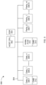
- FIG. 1 shows a schematic diagram of an example known data storage and accelerator system 100 suitable for utilizing an EC process for data storage.
- the data storage accelerator system 100 includes a host CPU 102, data storage devices 106-1,...,106-n allocated for storing data, parity storage devices 108-1,...,108-m allocated for storing parity information, and a PCIe accelerator 110 for performing, for example, an EC process.
- the host CPU 102, the data storage devices 106-1,...,106-n, the parity storage devices 108-1,...,108-m, and the PCIe accelerator 110 are connected together via a PCIe bus 104.
- the example system 100 shown includes n data storage devices 106-1 to 106-n and m parity storage devices 108-1 to 108-m allocated for storing parity information, where n and m may be positive integer numbers and may be determined based on the specific EC process utilized for generating parity information. For example, with a RS (12,4) process, four parity storage devices 108 are included for every twelve data storage devices 106 that are included.
- the PCIe accelerator 110 includes a PCIe interface (not shown) and one or more hardware accelerators (not shown) which may be, for example, field programmable gate arrays (FPGAs). Recovering lost data, for example as described previously, may be initiated by the host CPU 102 sending a proprietary command over the PCIe bus to the PCIe accelerator 110, which is received by the proprietary accelerator interface. In response to receiving the command from the host CPU 102, the proprietary accelerator interface signals the hardware accelerator to read the data from the non-corrupted data storage devices 106 and the parity information from the parity storage devices 108 and calculate the data. As described above, PCIe accelerators have the inherent problem of requiring customized drivers that require support across multiple OSes.
- FPGAs field programmable gate arrays
- Embodiments of the present disclosure provide an accelerator that utilizes a feature of the NVMe specification in order to reduce at least some of the above described problems inherent with PCIe accelerators.
- the NVMe accelerator may utilize NVMe commands to perform acceleration processes, rather than disk access functions as intended by the NVMe specification.
- the host CPU may treat an NVMe accelerator similar to an NVMe controller in order to perform acceleration processes utilizing the standard drivers that are already built into operating systems to support the NVMe standard.
- Facilitating acceleration utilizing standard drivers already in place reduces software engineering needed to implement hardware acceleration.
- Using the NVMe specification to control hardware acceleration is outside the scope and expectations of the NVMe specification and, therefore, some modification to the NVMe specification may be required to control hardware acceleration utilizing the NVMe specification, as described in more detail below.
- an example acceleration system 200 is shown in which a host CPU 202 sends NVMe commands, rather than PCIe commands, to an NVMe accelerator 204.
- the host CPU 202 may be connected to the NVMe accelerator via a PCIe bus 203.
- the NVMe accelerator 204 includes one or more hardware accelerators 208, 210, 212, each of which may be, for example, configured to perform a different acceleration function.
- the example NVMe accelerator 204 shown in FIG. 2 includes three hardware accelerators 208, 210, 212. However, other example NVMe accelerators may include more or fewer than three hardware accelerators, or a single hardware accelerator may be configured to perform multiple different acceleration processes.
- the example NVMe accelerator 204 shown in FIG. 2 includes an NVMe interface 206 that receives commands from the host CPU 202 and, based on the commands, signals one or more of the hardware accelerators 208, 210, 212 to perform the appropriate acceleration.
- the NVMe interface 206 is included within the NVMe accelerator 204 itself and thus the accelerator appears to the Host CPU 202 to be an NVMe storage device though it may not have associated persistent storage, such as an SSD, that the interface controls.
- the use of an NVMe interface 206 for an accelerator does not constrain the host CPU 202 to have other NVMe devices, such as NVMe SSDs, nor does it restrict the host CPU 202 from having other NVMe devices.
- the commands send from the host CPU 202 to the NVMe accelerator 204 may be, for example, standard NVMe disk access commands included in the NVMe specification, but the standard NVMe disk access commands are utilized as acceleration commands not disk access commands.
- the commands sent from the host CPU 202 may be customized commands that are supported by the vendor-specific registers and command space included within the NVMe specification, as described in more detail below.
- the system 300 also includes a host CPU 302, n data storage devices 306-1 to 306-n, and m parity storage devices 308-1 to 308-m connected via a PCIe bus 304, which may be substantially similar to the host CPU 102, the data storage devices 106, the parity storage devices 108, and the PCIe bus 104 described above with reference to FIG. 1 , and therefore are not further described here to avoid repetition.
- the NVMe accelerator 310 may be substantially similar to the NVMe accelerator 204 described in relation to FIG. 2 such that the host CPU 302 issues NVMe commands to the NVMe accelerator 310 to perform acceleration processes.
- the example system 300 shown in FIG. 3 includes CMBs 312 and 314 at data storage device 306-1 and the NVMe accelerator 310, respectively.
- the example shown in FIG. 3 includes two CMBs 312, 314, in other examples more or less than two CMBs may be included in the system 300.
- the CMBs 312, 314 enable the host CPU 302 to establish NVMe queues on the NVMe devices rather than in a random access memory associated with the host CPU 302, such as for example double data rate memory (DDR) 303.
- DDR double data rate memory
- Establishing NVMe queues on the CMBs 312,314 of the NVMe devices may be utilized to reduce the PCIe bandwidth used by the PCIe bus of the system 300 by reducing the PCIe traffic associated with DMA transfers.
- system 300 includes the NVMe accelerator 310, the data storage devices 306 and the parity storage devices 308 connected to the same PCIe bus 304, in other examples, some or all of the data storage devices 306, the parity storage devices 308 may be located remotely such that data is transferred over a network from a remote host.
- an example acceleration system 400 is shown in which acceleration may be performed on, for example, data from remote data storage devices (not shown) accessible over a network 424.
- the system 400 includes a host CPU 402 having an associated DDR memory 404, and an NVMe accelerator 410.
- the NVMe accelerator 410 is connected to the host CPU 402 via a PCIe switch 406 which is connected to the host CPU 402 via PCIe bus 405.
- the PCIe switch 406 enables the NVMe accelerator 410 being disconnected from the host CPU 402 and connected to other devices.
- the PCIe switch may be utilized to connect the NVMe accelerator to storage devices or other CPUs. Further, as described in more detail below with reference to FIG. 5 , the PCIe switch 406 may be utilized to connect the NVMe accelerator 410 to a network.
- the NVMe accelerator 410 includes a field programmable gate array (FPGA) 411 and optionally an onboard memory 420 on which a controller CMB 422 may be provided.
- the onboard memory 420 may be, for example, double data rate memory (DDR), or any other suitable type of memory.
- DDR double data rate memory
- the CMB 422 facilitates the host CPU 402 setting up NVMe queues on the NVMe accelerator 410 itself, reducing traffic over the PCIe bus 405.
- the FPGA 411 includes a controller 412, which includes a DMA engine, an NVMe interface 414, one or more hardware accelerators 416, and a DDR controller 418.
- the NVMe accelerator 410 may be controlled by standard NVMe commands, such as standard NVMe read and write commands, or may be controlled by vendor-specific commands, for example as described below.
- the DMA engine of the controller 412 may be utilized to transfer submission and completion commands and to transfer data to and from the hardware accelerators 416 in the event that a CMB is not utilized.
- the host CPU 402 may initiate an acceleration process by sending a standard NVMe disk access command, such as a disk write command, to the NVMe accelerator 410.
- the results of the acceleration process may be retrieved by the host CPU 402 by sending another standard NVMe disk access command, such as a read command, to the NVMe accelerator 410.
- standard NVMe disk access commands are utilized for acceleration control, rather than for disk access functions as intended by the NVMe specification.
- each hardware accelerator 416 may be associated with respective NVMe namespaces.
- the NVMe namespaces may be, for example, logical block addresses that would otherwise have been associated with an SSD.
- the disk access commands are sent in relation to an NVMe namespace that would otherwise have been associated with an SSD, but is instead used to enable hardware acceleration, and in some cases a specific type of hardware acceleration.
- the NVMe accelerator 410 is configured to perform two different acceleration processes: 1) a secured hash algorithm that generates a fixed 256-bit hash (SHA-256); and 2) EC.
- the SHA-256 may be associated with Namespace 1; EC encoding may be associated with Namespace 2; and EC decoding may be associated with Namespace 3.
- the host CPU 402 may send data to be EC encoded by the NVMe accelerator 410 by performing an NVMe write command to Namespace 2, and may retrieve the resultant EC encoded data by performing an NVMe read command to Namespace 2.
- the host CPU 402 may send vendor-specific commands to a submission queue of an NVMe accelerator 410.
- the submission queue may reside in either the DDR 404 of the host CPU 402 or the CMB 422 of the NVMe accelerator 410.
- the vendor-specific commands may be indicated by the opcode and facilitate the submission command providing customized control and command information to the accelerator 416 and the completion command providing customized feedback information from the controller 412 of the accelerator 416 to the host CPU 402.
- the NVMe accelerator 410 includes multiple accelerators 416, each accelerator 416 configured to perform a different acceleration process, different opcodes may be assigned to the different acceleration processes.
- data is provided to the accelerator 416 using the submission command via the DMA engine of the controller 412 and by pulling from a memory address provided in the vendor-specific command sent from the host CPU 402.
- the accelerator 416 performs the acceleration process specified by the opcode of the vendor-specific command, for example, an EC decoding acceleration on the data.
- the controller 412 provides a completion command back to the host CPU 402 indicating that acceleration is compete.
- the output data may be included in the completion command.
- the output data for a SHA-256 cryptographic hash function is 256 bits (32 bytes), which is small enough that it may be included in a completion command.
- the vendor-specific submission command that initiates the acceleration process may include a 64-bit address of a storage device to which the host CPU 402 wishes the output data to be written.
- the output data may be written directly to the 64-bit memory mapped address.
- the 64-bit memory address may be associated with a memory of, for example the computer that includes the host CPU and the NVMe accelerator 410, or on another local or remote PCIe attached device such as, for example, a CMB enabled NVMe drive connected to the NVMe accelerator 410 via the PCIe switch 406.
- the vendor-specific submission command includes a 64-bit address
- the completion command will be sent to the host CPU 402 only after the data transfer to the requested location is completed.
- the NVMe accelerator 410 may be configured such that the CMB 422 maps to an onboard memory 420, which is typically a DDR, of the NVMe accelerator 410 connected to the FPGA 411 using a DDR controller 418.
- input data and acceleration commands may be provided by the host CPU 402 by sending standard NVMe commands or vendor-specific commands and pulling the input data using the DMA Controller 412, as described above, or by writing the input data directly to the CMB 422.
- Output data generated by the hardware accelerator 416 processing the input data may be written directly to the CMB 422 or may be provided using a completion command as described above.
- the NVMe accelerator 410 may provide a vendor-specific completion message to the host CPU 402 that contains the memory mapped address to the results in CMB 422 in onboard memory 420 so the host CPU 402 can retrieve the output data.
- the host CPU 402 has the ability to retrieve output data from the onboard memory 420 and transmit the data to any other device including, for example, devices connected to the NVMe accelerator via the PCIe switch 406.
- Using the CMB 422 for data transfers lowers the bandwidth on the DMA engine of the controller 412 and may avoid a potential bottleneck in the controller 412.
- Using the CMB 422 for data transfers also removes the need for a host CPU 402 to provide a staging buffer and perform a memory copy between a data source, such as a hard drive, and an accelerator 416 because the data source can provide data directly to the accelerator 416.
- Using the CMB 422 to receive the data from one submission command does not force other submission commands to use the CMB 422 for their respective data and following commands may use the DMA engine of the controller 412 to pull data from host memory DDR 404. Bottlenecks in the DDR controller 418 and DMA engine of the controller 412 may be mitigated by using both data transfer mechanisms.
- the PCIe switch 406 may facilitate the NVMe accelerator 410 connecting with other devices over a network, such as, for example, storage devices or CPUs at remote locations.
- FIG. 5 shows an example of a system 500 in which a host CPU 526 does not have a locally connected hardware accelerator, but is able to access a remote NVMe accelerator 510 over a network 524 in order to perform acceleration processes without loading the remote CPU 502 at the location of the remote NVMe accelerator 510.
- the remote CPU 502, the DDR 504, the PCIe switch 506, the NVMe accelerator 510, the FPGA 511, the controller 512, the NVMe interface 514, the hardware accelerators 516, the DDR controller 518, the optional memory 520 having a CMB 522 are substantially similar to the host CPU 402, the DDR 404, the PCIe switch 406, the NVMe accelerator 410, the FPGA 411, the controller 412, the NVMe engine 414, the hardware accelerator 416, the DDR controller 418, the optional memory 420 having a CMB 422 described above with reference to FIG. 4 and therefore are not further described here to avoid repetition.
- the remote CPU 502 is connected to the NVMe accelerator over a PCIe bus 505. Further the PCIe switch 506 is connected to a remote direct access memory network interface card (RDMA NIC) 508 that facilitates connecting the NVMe accelerator 510 to a network 524.
- RDMA NIC remote direct access memory network interface card
- the host CPU 526 has an associated DDR 528.
- the host CPU 526 is connected to a PCIe switch 530 over a PCIe bus 529.
- the PCIe switch 530 is connected to a RDMA NIC 532 which facilitates connecting the host CPU 526 to the NVMe accelerator 510 over the network 524.
- the network 524 may be any suitable network that facilitates transmitting data between devices, including wired networks, wireless networks, or a combination of wired and wireless networks.
- the host CPU 526 is able to connect directly with the remote NVMe accelerator 510 to push data directly from, for example, the DDR 528 to the remote NVMe accelerator 510 without loading the remote CPU 502 and without the remote CPU 502 necessarily being aware that the transaction between the host CPU 526 and the remote NVMe accelerator 510 has taken place.
- data can be pulled from the remote NVMe accelerator 510 by the host CPU 526 without intervention or awareness from the remote CPU 502.
- the remote CPU 502 may also access the acceleration functionality of the NVMe accelerator 510, as described above. Therefore, the system 500 shown in FIG. 5 may facilitate a distributed network of NVMe accelerators 510 that may be shared among a plurality of CPUs in order reduce deployment costs in situations in which a dedicated NVMe accelerator is unwarranted.
- any number of host CPUs 526 may connect with the NVMe accelerator 510 over the network 524.
- the NVMe accelerator 510 may connect to any number of storage devices over the network 524.
- a challenge associated with a distributed accelerator in system 500 is managing quality of service for acceleration processes in view of CPUs 526 remote to the NVMe accelerator 510 pushing data to the NVMe accelerator 510 without the other CPUs being aware of the NVMe accelerator load.
- This challenge may be addressed by implementing vendor-specific commands that allow a CPU to query the NVMe accelerator 510 for the accelerator load data, such as for example the current and the average acceleration load. This query may facilitate a CPU finding an in-network NVMe accelerator 510 with the desired bandwidth to process the acceleration to be performed.
- the acceleration load statistics of the NVMe accelerator 510 can reside in CMB 522 allowing a CPU 502, 526 reading the load directly from the memory 520 of the NVMe accelerator 510.
- FIG. 6 a flow chart illustrating a method for controlling an accelerator using the NVMe specification is shown.
- the method may be implemented in any of the example NVMe accelerators described above.
- the method may be performed by, for example, a processor of an NVMe accelerator that performs instructions stored in a memory of the NVMe accelerator.
- a first NVMe command associated with an accelerator process is received at an NVMe interface of an NVMe accelerator from a host CPU.
- the format of the first NVMe command is the format of a standard NVMe command, such as a standard disk access command in accordance with the NVMe specification such as a read or write command.
- the first NVMe command is a standard NVMe read/write command that includes a namespace that would otherwise be associated with an SSD, where the included namespace is instead associated with the acceleration process.
- a vendor-specific command may include an address to which the result data generated by the acceleration process is to be written.
- the first NVMe command may be received from a host CPU that is local, or from a host CPU that is remote such that the first NVMe command is received over a network.
- the acceleration function associated with the received first NVMe command is determined. For example, as described above, if the first NVMe command is in the format of a standard NVMe command, then the determining at 604 may comprise determining the acceleration function associated with a namespace that would otherwise be associated with an SSD, but is now associated with an acceleration function, that is included within the first NVMe command. The determining at 604 may also include determining one of a plurality of hardware accelerators that are configured to perform the acceleration process associated with the first NVMe command.
- the acceleration process is performed by a hardware accelerator.
- Performing the acceleration process at 606 includes sending the input data to be processed to the hardware accelerator, or signalling the hardware accelerator to retrieve the input data.
- Performing the acceleration processes at 606 may also include signalling the acceleration hardware to write the generated result data to a particular address.
- a complete message is sent to the host CPU when the hardware accelerator has completed performing the acceleration process.
- the complete message may be a standard NVMe complete message, or may be a vendor-specific complete message.
- a vendor-specific complete message may include the result data if the result data is small enough to be included in the complete message. If the result data is written by the hardware accelerator to a particular memory address specified by the host CPU in the first NVMe command, then complete message may be sent once the result data has been completely written to the specified address.
- the vendor-specific NVMe complete message may include an address at which the result data has been written.
- a second NVMe command may be received from the host CPU to retrieve the result data and in response to receiving the second NVMe command, the result data may be sent.
- the second NVMe command may be, for example, a standard NVMe disk access command, such as a standard read or write command in accordance with the NVMe specification, or may be a vendor-specific command.
- the standard read/write command may include a namespace, where the included namespace is associated with the acceleration process, such that the result data from the acceleration process associated with the namespace is the data sent to the host CPU.
- a vendor-specific command may include an address to which the result data is to be sent to.
- Embodiments of the present disclosure facilitate performing hardware acceleration processes without utilizing specialized drivers that are software and hardware specific by controlling the hardware accelerator with NVMe commands.
- the NVMe commands may be based on standardized NVMe commands provided in the NVMe specification, or may be vendor-specific commands that are supported by the NVMe specification.
- the commands are sent to the NVMe accelerator by a host CPU which, in some embodiments, may be located remotely to the NVMe accelerator.
- the NVMe accelerator may include a CMB on which a host CPU may set up an NVMe queue in order to reduce PCIe traffic on a PCIe bus connecting the CPU and the NVMe accelerator.
- the CMB may also be used by a host CPU to transfer data for acceleration algorithms to remove host staging buffers, reduce bandwidth in the DMA controller, or to remove host memory copies.
- Embodiments of the disclosure can be represented as a computer program product stored in a machine-readable medium (also referred to as a computer-readable medium, a processor-readable medium, or a computer usable medium having a computer-readable program code embodied therein).
- the machine-readable medium can be any suitable tangible, non-transitory medium, including magnetic, optical, or electrical storage medium including a diskette, compact disk read only memory (CD-ROM), memory device (volatile or non-volatile), or similar storage mechanism.
- the machine-readable medium can contain various sets of instructions, code sequences, configuration information, or other data, which, when executed, cause a processor to perform steps in a method according to an embodiment of the disclosure.
Landscapes
- Engineering & Computer Science (AREA)
- Theoretical Computer Science (AREA)
- Physics & Mathematics (AREA)
- General Engineering & Computer Science (AREA)
- General Physics & Mathematics (AREA)
- Human Computer Interaction (AREA)
- Software Systems (AREA)
- Computer Hardware Design (AREA)
- Advance Control (AREA)
- Information Transfer Systems (AREA)
Claims (15)
- Verfahren zum Steuern eines Hardwarebeschleunigers (208, 210, 212, 416, 516), der dazu ausgelegt ist, zu verarbeitende Eingangsdaten zu empfangen und verarbeitete Eingangsdaten zurückzugeben, wobei das Verfahren Folgendes umfasst:Empfangen eines ersten nichtflüchtigen Speicherexpress(NVMe)-Befehls an einer NVMe-Schnittstelle (206, 414, 514) in Kommunikation mit dem Hardwarebeschleuniger (208, 210, 212, 416, 516) von einem Host (202, 302, 402, 502), wobei der erste NVMe-Befehl ein Format eines Disklese- oder -schreibbefehls aufweist, aber mit einer Beschleunigungsfunktion verknüpft ist, die keine Disklese- oder -schreibfunktion ist,und wobei der erste NVMe-Befehl einen ersten Namensraum einer Vielzahl von Namensräumen beinhaltet, wobei jeder der Namensräume ein Format eines Namensraums aufweist, der mit einem Festkörperlaufwerk (SSD) verknüpft ist, aber mit einer jeweiligen einer Vielzahl von Beschleunigungsfunktionen und nicht mit einem SSD verknüpft ist;Bestimmen der Beschleunigungsfunktion, die mit dem empfangenen ersten NVMe-Befehl verknüpft ist, durch die NVMe-Schnittstelle (206, 414, 514) auf Basis des ersten Namensraums, wobei die Beschleunigungsfunktion eine andere Funktion ist als eine Disklese- oder - schreibfunktion;Durchführen der Beschleunigungsfunktion am Hardwarebeschleuniger (208, 210, 212, 416, 516), um Ergebnisdaten zu erzeugen.
- Verfahren nach Anspruch 1, das ferner Folgendes umfasst:
Empfangen eines zweiten NVMe-Befehls an der NVMe-Schnittstelle (206, 414, 514) vom Host (202, 302, 402, 502), wobei der zweite NVMe-Befehl mit einer Anforderung von Ergebnisdaten verknüpft ist, die durch die Durchführung der Beschleunigungsfunktion erzeugt werden und ein Format einer Disklese- oder -schreibfunktion aufweisen, aber mit einer Hardwarebeschleunigerübertragungsfunktion und nicht mit einer Disklese- oder -schreibfunktion verknüpft sind, und in Reaktion auf das Empfangen des zweiten NVMe-Befehls Übertragen der Ergebnisdaten am Hardwarebeschleuniger (208, 210, 212, 416, 516). - Verfahren nach Anspruch 2, wobei der erste NVMe-Befehl, der vom Host (202, 302, 402, 502) empfangen wird, als ein NVMe-Schreibbefehl formatiert ist und der zweite NVMe-Befehl als ein NVMe-Lesebefehl formatiert ist.
- Verfahren nach Anspruch 2, wobei der zweite NVMe-Befehl den ersten Namensraum beinhaltet, wobei einer des ersten NVMe-Befehls und des zweiten NVMe-Befehls als ein Schreibbefehl für den ersten Namensraum formatiert ist und der andere des ersten und des zweiten NVMe-Befehls als ein Lesebefehl für den ersten Namensraum formatiert ist.
- Verfahren nach Anspruch 1, das ferner Folgendes umfasst:Bestimmen an der NVMe-Schnittstelle (206, 414, 514), dass der Hardwarebeschleuniger (208, 210, 212, 416, 516) das Durchführen der Beschleunigungsfunktion abgeschlossen hat; undSenden einer NVMe-Abschlussnachricht, die anzeigt, dass die Beschleunigungsfunktion durchgeführt wurde, von der NVMe-Schnittstelle (206, 414, 514) an den Host (202, 302, 402, 502) .
- Verfahren nach Anspruch 2, wobei der erste NVMe-Befehl eine erste Speicheradresse einer Speichervorrichtung beinhaltet, von der die Eingangsdaten zu lesen sind, und wobei der Speicher ferner zusätzlich zum Durchführen der Beschleunigungsfunktion an den Eingangsdaten das Lesen der Eingangsdaten beinhaltet, die an der ersten Speicheradresse gespeichert sind, die im ersten NVMe-Befehl beinhaltet ist, um die Ergebnisdaten zu erzeugen.
- Verfahren nach Anspruch 2, wobei der zweite NVMe-Befehl eine zweite Speicheradresse einer Speichervorrichtung beinhaltet, zu der die Ergebnisdaten zu übertragen sind, und wobei das Übertragen der Ergebnisdaten in Reaktion auf das Empfangen des zweiten NVMe-Befehls das Übertragen der Ergebnisdaten zum Speichern der Ergebnisdaten an der zweiten Speicheradresse zur Speichervorrichtung beinhaltet.
- Verfahren nach Anspruch 1, wobei das Empfangen des ersten NVMe-Befehls an der NVMe-Schnittstelle (206, 414, 514) das Empfangen des ersten NVMe-Befehls an einem Steuerungsspeicherpuffer (314, 422, 522) der NVMe-Schnittstelle (206, 414, 514) umfasst.
- Beschleuniger (204, 310, 410, 510) zum Durchführen einer Beschleunigungsfunktion, wobei der Beschleuniger Folgendes umfasst:
eine NMVe-Schnittstelle (206, 414, 514) und einen Hardwarebeschleuniger (208, 210, 212, 416, 516), der mit der NVMe-Schnittstelle (206, 414, 514) in Kommunikation steht und dazu ausgelegt ist, die Beschleunigungsfunktion durchzuführen, wobei die NVMe-Schnittstelle (206, 414, 514) zu Folgendem ausgelegt ist:Empfangen eines ersten NVMe-Befehls von einem Host (202, 302, 402, 502), wobei der erste NVMe-Befehl ein Format einer Disklese- oder -schreibfunktion aufweist, aber mit einer Beschleunigungsfunktion verknüpft ist, die nicht ohne Bezug zu einer Disklese- oder -schreibfunktion ist, und wobei der erste NVMe-Befehl einen ersten Namensraum einer Vielzahl von Namensräumen beinhaltet, wobei jeder der Namensräume ein Format eines Namensraums aufweist, der mit einem Festkörperlaufwerk (SSD) verknüpft ist, aber mit einer jeweiligen einer Vielzahl von Beschleunigungsfunktionen und nicht mit einem SSD verknüpft ist;Bestimmen einer Beschleunigungsfunktion, die mit dem empfangenen ersten NVMe-Befehl verknüpft ist, auf Basis des ersten Namensraums, wobei die Beschleunigungsfunktion eine andere Funktion ist als eine Disklese- oder -schreibfunktion;Signalisieren des Hardwarebeschleunigers (208, 210, 212, 416, 516) zum Durchführen der Beschleunigungsfunktion. - Beschleuniger (204, 310, 410, 510) nach Anspruch 9, wobei die NVMe-Schnittstelle (206, 414, 514) ferner zu Folgendem ausgelegt ist:Empfangen eines zweiten NVMe-Befehls vom Host (202, 302, 402, 502), wobei der zweite NVMe-Befehl mit einer Anforderung von Ergebnisdaten verknüpft ist, die durch die Durchführung der Beschleunigungsfunktion erzeugt werden und ein Format einer Disklese- oder - schreibfunktion aufweisen, aber mit einer Hardwarebeschleunigerübertragungsfunktion verknüpft und nicht ohne Bezug zu einer Disklese- oder -schreibfunktion ist, undin Reaktion auf das Empfangen des zweiten NVMe-Befehls Signalisieren des Hardwarebeschleunigers (208, 210, 212, 416, 516) zum Übertragen der Ergebnisdaten.
- Beschleuniger (204, 310, 410, 510) nach Anspruch 10, wobei der erste NVMe-Befehl, der vom Host (202, 302, 402, 502) empfangen wird, als ein NVMe-Schreibbefehl formatiert ist und der zweite NVMe-Befehl als ein NVMe-Lesebefehl formatiert ist.
- Beschleuniger (204, 310, 410, 510) nach Anspruch 10, wobei der zweite NVMe-Befehl den ersten Namensraum beinhaltet und wobei einer des ersten NVMe-Befehls und des zweiten NVMe-Befehls als ein Schreibbefehl für den ersten Namensraum formatiert ist und der andere des ersten und des zweiten NVMe-Befehls als ein Lesebefehl für den ersten Namensraum formatiert ist.
- Beschleuniger (204, 310, 410, 510) nach Anspruch 9, wobei die NVMe-Schnittstelle (206, 414, 514) ferner zu Folgendem ausgelegt ist:Bestimmen, dass der Hardwarebeschleuniger (208, 210, 212, 416, 516) das Durchführen der Beschleunigungsfunktion abgeschlossen hat; undSenden einer NVMe-Abschlussnachricht, die anzeigt, dass die Beschleunigungsfunktion durchgeführt wurde, an den Host (202, 302, 402, 502).
- Beschleuniger (204, 310, 410, 510) nach Anspruch 10, wobei der erste NVMe-Befehl eine erste Speicheradresse einer Speichervorrichtung beinhaltet, von der die Eingangsdaten zu lesen sind, und wobei die NVMe-Schnittstelle (206, 414, 514) ferner dazu ausgelegt ist, zusätzlich zum Signalisieren des Hardwarebeschleunigers (208, 210, 212, 416, 516) zum Durchführen der Beschleunigungsfunktion an den Eingangsdaten den Hardwarebeschleuniger (208, 210, 212, 416, 516) zum Lesen der Eingangsdaten, die an der ersten Speicheradresse gespeichert sind, die im ersten NVMe-Befehl beinhaltet ist, zu signalisieren, um die Ergebnisdaten zu erzeugen.
- Beschleuniger (204, 310, 410, 510) nach Anspruch 9, der ferner einen Steuerungsspeicherpuffer (CMB) (314, 422, 522) beinhaltet, wobei das Empfangen des ersten NVMe-Befehls an der NVMe-Schnittstelle (206, 414, 514) das Empfangen des ersten NVMe-Befehls am CMB (314, 422, 522) umfasst.
Applications Claiming Priority (2)
| Application Number | Priority Date | Filing Date | Title |
|---|---|---|---|
| US201762500794P | 2017-05-03 | 2017-05-03 | |
| PCT/CA2018/050520 WO2018201249A1 (en) | 2017-05-03 | 2018-05-02 | Apparatus and method for controlling data acceleration |
Publications (4)
| Publication Number | Publication Date |
|---|---|
| EP3616073A1 EP3616073A1 (de) | 2020-03-04 |
| EP3616073A4 EP3616073A4 (de) | 2021-02-17 |
| EP3616073B1 true EP3616073B1 (de) | 2024-08-21 |
| EP3616073C0 EP3616073C0 (de) | 2024-08-21 |
Family
ID=64015763
Family Applications (1)
| Application Number | Title | Priority Date | Filing Date |
|---|---|---|---|
| EP18795114.0A Active EP3616073B1 (de) | 2017-05-03 | 2018-05-02 | Vorrichtung und verfahren zur steuerung von datenbeschleunigung |
Country Status (5)
| Country | Link |
|---|---|
| US (1) | US10996892B2 (de) |
| EP (1) | EP3616073B1 (de) |
| CN (1) | CN110770710B (de) |
| CA (1) | CA3062336C (de) |
| WO (1) | WO2018201249A1 (de) |
Families Citing this family (43)
| Publication number | Priority date | Publication date | Assignee | Title |
|---|---|---|---|---|
| US12481612B2 (en) | 2018-03-02 | 2025-11-25 | Samsung Electronics Co., Ltd. | Mechanism to identify FPGA and SSD pairing in a multi-device environment |
| US10635609B2 (en) * | 2018-03-02 | 2020-04-28 | Samsung Electronics Co., Ltd. | Method for supporting erasure code data protection with embedded PCIE switch inside FPGA+SSD |
| US12505053B2 (en) | 2018-03-02 | 2025-12-23 | Samsung Electronics Co., Ltd. | Method for supporting erasure code data protection with embedded PCIe switch inside FPGA+SSD |
| US11340949B2 (en) * | 2018-05-08 | 2022-05-24 | Telefonaktiebolaget Lm Ericsson (Publ) | Method and node for managing a request for hardware acceleration by means of an accelerator device |
| US11144357B2 (en) | 2018-05-25 | 2021-10-12 | International Business Machines Corporation | Selecting hardware accelerators based on score |
| US10977098B2 (en) * | 2018-08-14 | 2021-04-13 | International Business Machines Corporation | Automatically deploying hardware accelerators based on requests from users |
| US10892944B2 (en) | 2018-11-29 | 2021-01-12 | International Business Machines Corporation | Selecting and using a cloud-based hardware accelerator |
| US10860504B2 (en) | 2018-12-05 | 2020-12-08 | New Century Technologies Ltd. | Peripheral device with embedded video codec functionality |
| US11868284B2 (en) | 2018-12-05 | 2024-01-09 | Rongming Microelectronics (Jinan) Co., Ltd. | Peripheral device with embedded video codec functionality |
| CN109597786B (zh) * | 2018-12-05 | 2022-03-11 | 镕铭微电子(济南)有限公司 | 主机与硬件加速模块的交互方法、硬件加速设备及介质 |
| KR102659832B1 (ko) * | 2019-03-05 | 2024-04-22 | 삼성전자주식회사 | 데이터 저장 장치 및 시스템 |
| US11762695B2 (en) * | 2019-03-29 | 2023-09-19 | Lenovo Enterprise Solutions (Singapore) Pte. Ltd. | Transparent memory management for over-subscribed accelerators |
| US11016781B2 (en) * | 2019-04-26 | 2021-05-25 | Samsung Electronics Co., Ltd. | Methods and memory modules for enabling vendor specific functionalities |
| US10970246B2 (en) * | 2019-05-03 | 2021-04-06 | Intel Corporation | Technologies for remote networked accelerators |
| US11157212B2 (en) | 2019-12-19 | 2021-10-26 | Seagate Technology, Llc | Virtual controller memory buffer |
| US10910048B1 (en) | 2020-01-16 | 2021-02-02 | Micron Technology, Inc. | Extended memory communication |
| US11409466B2 (en) | 2020-01-29 | 2022-08-09 | Western Digital Technologies, Inc. | Access control in CMB/PMR virtualization environment |
| US20210373951A1 (en) * | 2020-05-28 | 2021-12-02 | Samsung Electronics Co., Ltd. | Systems and methods for composable coherent devices |
| US11733918B2 (en) | 2020-07-28 | 2023-08-22 | Samsung Electronics Co., Ltd. | Systems and methods for processing commands for storage devices |
| US11789634B2 (en) | 2020-07-28 | 2023-10-17 | Samsung Electronics Co., Ltd. | Systems and methods for processing copy commands |
| CN112256601B (zh) * | 2020-10-19 | 2023-04-21 | 苏州凌云光工业智能技术有限公司 | 数据存取控制方法、嵌入式存储系统及嵌入式设备 |
| KR20220064230A (ko) | 2020-11-11 | 2022-05-18 | 삼성전자주식회사 | 다중 프로토콜에 기초하여 메모리에 액세스하기 위한 시스템, 장치 및 방법 |
| CN112486574B (zh) * | 2020-12-16 | 2024-07-05 | 江苏国科微电子有限公司 | 一种完成队列的回复管理方法、装置、设备及存储介质 |
| CN112527205B (zh) * | 2020-12-16 | 2024-12-06 | 江苏国科微电子有限公司 | 一种数据安全防护方法、装置、设备及介质 |
| CN112711442B (zh) * | 2020-12-29 | 2024-09-03 | 北京浪潮数据技术有限公司 | 一种主机命令写入方法、设备、系统及可读存储介质 |
| KR102890134B1 (ko) | 2021-01-06 | 2025-11-21 | 삼성전자 주식회사 | 메모리 장치를 제어하는 가속기, 이를 포함하는 컴퓨팅 시스템 및 가속기의 동작방법 |
| US12210470B2 (en) | 2021-08-03 | 2025-01-28 | Samsung Electronics Co., Ltd. | Systems, methods, and apparatus to identify functions for computational devices |
| CN115455396A (zh) * | 2022-03-08 | 2022-12-09 | 神盾股份有限公司 | 用于处理指纹信息的方法、硬件加速器及指纹识别设备 |
| US12475075B2 (en) * | 2022-03-10 | 2025-11-18 | Intel Corporation | Circuits and methods for coherent writing to host systems |
| CN114415974B (zh) * | 2022-03-28 | 2022-06-03 | 北京得瑞领新科技有限公司 | Ssd操作逻辑空间的方法、装置、存储介质及ssd设备 |
| CN115033186B (zh) * | 2022-08-09 | 2022-11-01 | 北京得瑞领新科技有限公司 | 双端口NVMe控制器及读写命令处理方法 |
| US20240094950A1 (en) * | 2022-09-16 | 2024-03-21 | Western Digital Technologies, Inc. | Block layer persistent memory buffer |
| CN115562574B (zh) * | 2022-09-23 | 2026-03-27 | 山东云海国创云计算装备产业创新中心有限公司 | 一种NVMe加速系统、方法、设备及可读介质 |
| KR20240079650A (ko) * | 2022-11-29 | 2024-06-05 | 삼성전자주식회사 | 다이렉트 스토리지 기능을 지원하는 스토리지 장치 및 스토리지 시스템 |
| KR20240084902A (ko) | 2022-12-07 | 2024-06-14 | 삼성전자주식회사 | 연산 스토리지 장치 및 그 구동 방법 |
| US12346343B2 (en) * | 2022-12-12 | 2025-07-01 | Maxlinear, Inc. | Data transform acceleration using metadata stored in accelerator memory |
| CN116027985A (zh) * | 2023-02-10 | 2023-04-28 | 山东云海国创云计算装备产业创新中心有限公司 | 一种提高NVMe加速器可用性的方法、装置、设备及介质 |
| CN116627880B (zh) * | 2023-05-23 | 2024-01-30 | 无锡众星微系统技术有限公司 | 一种支持RAID加速的PCIe Switch及其RAID加速方法 |
| US12271606B2 (en) | 2023-07-31 | 2025-04-08 | Dell Products L.P. | Software raid/management communication system |
| CN116909484B (zh) * | 2023-08-02 | 2024-08-02 | 中科驭数(北京)科技有限公司 | 数据处理方法、装置、设备及计算机可读存储介质 |
| US12511195B2 (en) * | 2023-08-21 | 2025-12-30 | Microchip Technology Incorporated | Non-volatile memory express transport protocol messaging for parity generation |
| CN117472813B (zh) * | 2023-11-09 | 2025-03-25 | 中科驭数(北京)科技有限公司 | NVMe主机、硬盘与内存之间的数据传输方法及系统 |
| CN120371752A (zh) * | 2024-02-29 | 2025-07-25 | 上海玄戒技术有限公司 | 一种数据加速器、驱动装置及芯片 |
Citations (1)
| Publication number | Priority date | Publication date | Assignee | Title |
|---|---|---|---|---|
| WO2008027091A1 (en) * | 2006-08-28 | 2008-03-06 | Tableau, Llc | Method and system for password recovery using a hardware accelerator |
Family Cites Families (7)
| Publication number | Priority date | Publication date | Assignee | Title |
|---|---|---|---|---|
| US10360176B2 (en) * | 2012-01-17 | 2019-07-23 | Intel Corporation | Techniques for command validation for access to a storage device by a remote client |
| US9003071B2 (en) * | 2013-03-13 | 2015-04-07 | Futurewei Technologies, Inc. | Namespace access control in NVM express PCIe NVM with SR-IOV |
| US9323610B2 (en) | 2014-01-30 | 2016-04-26 | Sandisk Technologies Inc. | Non-blocking commands |
| US9501245B2 (en) * | 2014-05-02 | 2016-11-22 | Cavium, Inc. | Systems and methods for NVMe controller virtualization to support multiple virtual machines running on a host |
| US20170228173A9 (en) * | 2014-05-02 | 2017-08-10 | Cavium, Inc. | Systems and methods for enabling local caching for remote storage devices over a network via nvme controller |
| US20160094619A1 (en) | 2014-09-26 | 2016-03-31 | Jawad B. Khan | Technologies for accelerating compute intensive operations using solid state drives |
| CN107241913B (zh) | 2015-02-25 | 2020-06-19 | 株式会社日立制作所 | 信息处理装置 |
-
2018
- 2018-05-02 EP EP18795114.0A patent/EP3616073B1/de active Active
- 2018-05-02 CN CN201880038486.4A patent/CN110770710B/zh active Active
- 2018-05-02 US US16/335,916 patent/US10996892B2/en active Active
- 2018-05-02 CA CA3062336A patent/CA3062336C/en active Active
- 2018-05-02 WO PCT/CA2018/050520 patent/WO2018201249A1/en not_active Ceased
Patent Citations (1)
| Publication number | Priority date | Publication date | Assignee | Title |
|---|---|---|---|---|
| WO2008027091A1 (en) * | 2006-08-28 | 2008-03-06 | Tableau, Llc | Method and system for password recovery using a hardware accelerator |
Also Published As
| Publication number | Publication date |
|---|---|
| EP3616073A4 (de) | 2021-02-17 |
| CN110770710B (zh) | 2023-09-05 |
| EP3616073C0 (de) | 2024-08-21 |
| EP3616073A1 (de) | 2020-03-04 |
| WO2018201249A1 (en) | 2018-11-08 |
| US10996892B2 (en) | 2021-05-04 |
| US20200050401A1 (en) | 2020-02-13 |
| CA3062336C (en) | 2022-07-12 |
| CN110770710A (zh) | 2020-02-07 |
| CA3062336A1 (en) | 2018-11-08 |
Similar Documents
| Publication | Publication Date | Title |
|---|---|---|
| EP3616073B1 (de) | Vorrichtung und verfahren zur steuerung von datenbeschleunigung | |
| TWI814975B (zh) | 用於利用自我調整寫緩衝區釋放的存儲介質編程方法與裝置、以及其系統單晶片 | |
| US10423568B2 (en) | Apparatus and method for transferring data and commands in a memory management environment | |
| US9557922B2 (en) | System and method for peer-to-peer PCIe storage transfers | |
| US12361144B2 (en) | Methods and apparatus for offloading encryption | |
| US10048962B2 (en) | Apparatus, system, and method for non-volatile data storage and retrieval | |
| US20210004165A1 (en) | Dummy Host Command Generation For Supporting Higher Maximum Data Transfer Sizes (MDTS) | |
| US7460531B2 (en) | Method, system, and program for constructing a packet | |
| US6105076A (en) | Method, system, and program for performing data transfer operations on user data | |
| JP6649989B2 (ja) | ストレージシステム及びその制御方法 | |
| WO2003043254A9 (en) | Transferring data using direct memory access | |
| KR20200101982A (ko) | NVMe 기반의 데이터 판독 방법, 장치, 및 시스템 | |
| US20210132858A1 (en) | Quality of Service (QOS) System and Method for Non-Volatile Memory Express Devices | |
| US20200319819A1 (en) | Method and Apparatus for Improving Parity Redundant Array of Independent Drives Write Latency in NVMe Devices | |
| US20110154165A1 (en) | Storage apparatus and data transfer method | |
| US20170139607A1 (en) | Method and system for shared direct access storage | |
| US10191690B2 (en) | Storage system, control device, memory device, data access method, and program recording medium | |
| US10733118B2 (en) | Computer system, communication device, and storage control method with DMA transfer of data | |
| EP2183663B1 (de) | Massenspeichersystem mit verbesserter nutzung der pufferkapazität | |
| KR100638378B1 (ko) | 디스크 제어장치의 메모리 구조에 대한 시스템 및 방법 | |
| JP2011192053A (ja) | ディスクアレイ装置、ディスクアレイシステム、及びキャッシュ制御方法 | |
| KR100986131B1 (ko) | 레이드 기능을 지원하는 솔리드 스테이트 디스크 | |
| JP2017130002A (ja) | ストレージ制御装置および制御プログラム | |
| US20250377883A1 (en) | Methods and systems for updating device firmware using a bootloader trap in immutable storage memory | |
| WO2017090517A1 (ja) | ソフトウェアストレージユニット、バックアップ方法、およびバックアップ制御プログラムが記録された記録媒体 |
Legal Events
| Date | Code | Title | Description |
|---|---|---|---|
| STAA | Information on the status of an ep patent application or granted ep patent |
Free format text: STATUS: THE INTERNATIONAL PUBLICATION HAS BEEN MADE |
|
| PUAI | Public reference made under article 153(3) epc to a published international application that has entered the european phase |
Free format text: ORIGINAL CODE: 0009012 |
|
| STAA | Information on the status of an ep patent application or granted ep patent |
Free format text: STATUS: REQUEST FOR EXAMINATION WAS MADE |
|
| 17P | Request for examination filed |
Effective date: 20191126 |
|
| AK | Designated contracting states |
Kind code of ref document: A1 Designated state(s): AL AT BE BG CH CY CZ DE DK EE ES FI FR GB GR HR HU IE IS IT LI LT LU LV MC MK MT NL NO PL PT RO RS SE SI SK SM TR |
|
| AX | Request for extension of the european patent |
Extension state: BA ME |
|
| DAV | Request for validation of the european patent (deleted) | ||
| DAX | Request for extension of the european patent (deleted) | ||
| A4 | Supplementary search report drawn up and despatched |
Effective date: 20210115 |
|
| RIC1 | Information provided on ipc code assigned before grant |
Ipc: G06F 15/76 20060101AFI20210111BHEP Ipc: G06F 9/06 20060101ALI20210111BHEP Ipc: G06F 13/00 20060101ALI20210111BHEP Ipc: G06F 3/06 20060101ALI20210111BHEP Ipc: G06F 15/00 20060101ALI20210111BHEP |
|
| STAA | Information on the status of an ep patent application or granted ep patent |
Free format text: STATUS: EXAMINATION IS IN PROGRESS |
|
| 17Q | First examination report despatched |
Effective date: 20220610 |
|
| REG | Reference to a national code |
Ref country code: DE Ipc: G06F0003060000 Ref country code: DE Ref legal event code: R079 Ref document number: 602018073387 Country of ref document: DE Free format text: PREVIOUS MAIN CLASS: G06F0015000000 Ipc: G06F0003060000 |
|
| GRAP | Despatch of communication of intention to grant a patent |
Free format text: ORIGINAL CODE: EPIDOSNIGR1 |
|
| STAA | Information on the status of an ep patent application or granted ep patent |
Free format text: STATUS: GRANT OF PATENT IS INTENDED |
|
| RIC1 | Information provided on ipc code assigned before grant |
Ipc: G06F 9/50 20060101ALI20240226BHEP Ipc: G06F 15/76 20060101ALI20240226BHEP Ipc: G06F 3/06 20060101AFI20240226BHEP |
|
| INTG | Intention to grant announced |
Effective date: 20240318 |
|
| GRAS | Grant fee paid |
Free format text: ORIGINAL CODE: EPIDOSNIGR3 |
|
| GRAA | (expected) grant |
Free format text: ORIGINAL CODE: 0009210 |
|
| STAA | Information on the status of an ep patent application or granted ep patent |
Free format text: STATUS: THE PATENT HAS BEEN GRANTED |
|
| AK | Designated contracting states |
Kind code of ref document: B1 Designated state(s): AL AT BE BG CH CY CZ DE DK EE ES FI FR GB GR HR HU IE IS IT LI LT LU LV MC MK MT NL NO PL PT RO RS SE SI SK SM TR |
|
| REG | Reference to a national code |
Ref country code: GB Ref legal event code: FG4D |
|
| REG | Reference to a national code |
Ref country code: CH Ref legal event code: EP |
|
| REG | Reference to a national code |
Ref country code: DE Ref legal event code: R096 Ref document number: 602018073387 Country of ref document: DE |
|
| REG | Reference to a national code |
Ref country code: IE Ref legal event code: FG4D |
|
| U01 | Request for unitary effect filed |
Effective date: 20240918 |
|
| U07 | Unitary effect registered |
Designated state(s): AT BE BG DE DK EE FI FR IT LT LU LV MT NL PT RO SE SI Effective date: 20241008 |
|
| PG25 | Lapsed in a contracting state [announced via postgrant information from national office to epo] |
Ref country code: NO Free format text: LAPSE BECAUSE OF FAILURE TO SUBMIT A TRANSLATION OF THE DESCRIPTION OR TO PAY THE FEE WITHIN THE PRESCRIBED TIME-LIMIT Effective date: 20241121 |
|
| PG25 | Lapsed in a contracting state [announced via postgrant information from national office to epo] |
Ref country code: PL Free format text: LAPSE BECAUSE OF FAILURE TO SUBMIT A TRANSLATION OF THE DESCRIPTION OR TO PAY THE FEE WITHIN THE PRESCRIBED TIME-LIMIT Effective date: 20240821 Ref country code: GR Free format text: LAPSE BECAUSE OF FAILURE TO SUBMIT A TRANSLATION OF THE DESCRIPTION OR TO PAY THE FEE WITHIN THE PRESCRIBED TIME-LIMIT Effective date: 20241122 |
|
| PG25 | Lapsed in a contracting state [announced via postgrant information from national office to epo] |
Ref country code: IS Free format text: LAPSE BECAUSE OF FAILURE TO SUBMIT A TRANSLATION OF THE DESCRIPTION OR TO PAY THE FEE WITHIN THE PRESCRIBED TIME-LIMIT Effective date: 20241221 |
|
| PG25 | Lapsed in a contracting state [announced via postgrant information from national office to epo] |
Ref country code: HR Free format text: LAPSE BECAUSE OF FAILURE TO SUBMIT A TRANSLATION OF THE DESCRIPTION OR TO PAY THE FEE WITHIN THE PRESCRIBED TIME-LIMIT Effective date: 20240821 |
|
| PG25 | Lapsed in a contracting state [announced via postgrant information from national office to epo] |
Ref country code: ES Free format text: LAPSE BECAUSE OF FAILURE TO SUBMIT A TRANSLATION OF THE DESCRIPTION OR TO PAY THE FEE WITHIN THE PRESCRIBED TIME-LIMIT Effective date: 20240821 Ref country code: RS Free format text: LAPSE BECAUSE OF FAILURE TO SUBMIT A TRANSLATION OF THE DESCRIPTION OR TO PAY THE FEE WITHIN THE PRESCRIBED TIME-LIMIT Effective date: 20241121 |
|
| PG25 | Lapsed in a contracting state [announced via postgrant information from national office to epo] |
Ref country code: RS Free format text: LAPSE BECAUSE OF FAILURE TO SUBMIT A TRANSLATION OF THE DESCRIPTION OR TO PAY THE FEE WITHIN THE PRESCRIBED TIME-LIMIT Effective date: 20241121 Ref country code: PL Free format text: LAPSE BECAUSE OF FAILURE TO SUBMIT A TRANSLATION OF THE DESCRIPTION OR TO PAY THE FEE WITHIN THE PRESCRIBED TIME-LIMIT Effective date: 20240821 Ref country code: NO Free format text: LAPSE BECAUSE OF FAILURE TO SUBMIT A TRANSLATION OF THE DESCRIPTION OR TO PAY THE FEE WITHIN THE PRESCRIBED TIME-LIMIT Effective date: 20241121 Ref country code: IS Free format text: LAPSE BECAUSE OF FAILURE TO SUBMIT A TRANSLATION OF THE DESCRIPTION OR TO PAY THE FEE WITHIN THE PRESCRIBED TIME-LIMIT Effective date: 20241221 Ref country code: HR Free format text: LAPSE BECAUSE OF FAILURE TO SUBMIT A TRANSLATION OF THE DESCRIPTION OR TO PAY THE FEE WITHIN THE PRESCRIBED TIME-LIMIT Effective date: 20240821 Ref country code: GR Free format text: LAPSE BECAUSE OF FAILURE TO SUBMIT A TRANSLATION OF THE DESCRIPTION OR TO PAY THE FEE WITHIN THE PRESCRIBED TIME-LIMIT Effective date: 20241122 Ref country code: ES Free format text: LAPSE BECAUSE OF FAILURE TO SUBMIT A TRANSLATION OF THE DESCRIPTION OR TO PAY THE FEE WITHIN THE PRESCRIBED TIME-LIMIT Effective date: 20240821 |
|
| PG25 | Lapsed in a contracting state [announced via postgrant information from national office to epo] |
Ref country code: SM Free format text: LAPSE BECAUSE OF FAILURE TO SUBMIT A TRANSLATION OF THE DESCRIPTION OR TO PAY THE FEE WITHIN THE PRESCRIBED TIME-LIMIT Effective date: 20240821 |
|
| PG25 | Lapsed in a contracting state [announced via postgrant information from national office to epo] |
Ref country code: CZ Free format text: LAPSE BECAUSE OF FAILURE TO SUBMIT A TRANSLATION OF THE DESCRIPTION OR TO PAY THE FEE WITHIN THE PRESCRIBED TIME-LIMIT Effective date: 20240821 |
|
| PG25 | Lapsed in a contracting state [announced via postgrant information from national office to epo] |
Ref country code: SK Free format text: LAPSE BECAUSE OF FAILURE TO SUBMIT A TRANSLATION OF THE DESCRIPTION OR TO PAY THE FEE WITHIN THE PRESCRIBED TIME-LIMIT Effective date: 20240821 |
|
| PLBE | No opposition filed within time limit |
Free format text: ORIGINAL CODE: 0009261 |
|
| STAA | Information on the status of an ep patent application or granted ep patent |
Free format text: STATUS: NO OPPOSITION FILED WITHIN TIME LIMIT |
|
| U20 | Renewal fee for the european patent with unitary effect paid |
Year of fee payment: 8 Effective date: 20250526 |
|
| PGFP | Annual fee paid to national office [announced via postgrant information from national office to epo] |
Ref country code: GB Payment date: 20250520 Year of fee payment: 8 |
|
| 26N | No opposition filed |
Effective date: 20250522 |
|
| REG | Reference to a national code |
Ref country code: CH Ref legal event code: H13 Free format text: ST27 STATUS EVENT CODE: U-0-0-H10-H13 (AS PROVIDED BY THE NATIONAL OFFICE) Effective date: 20251223 |
|
| PG25 | Lapsed in a contracting state [announced via postgrant information from national office to epo] |
Ref country code: CH Free format text: LAPSE BECAUSE OF NON-PAYMENT OF DUE FEES Effective date: 20250531 |
|
| PG25 | Lapsed in a contracting state [announced via postgrant information from national office to epo] |
Ref country code: MC Free format text: LAPSE BECAUSE OF FAILURE TO SUBMIT A TRANSLATION OF THE DESCRIPTION OR TO PAY THE FEE WITHIN THE PRESCRIBED TIME-LIMIT Effective date: 20240821 |
|
| PG25 | Lapsed in a contracting state [announced via postgrant information from national office to epo] |
Ref country code: IE Free format text: LAPSE BECAUSE OF NON-PAYMENT OF DUE FEES Effective date: 20250502 |