EP3617858A1 - Wellenleiterbasiertes berührungssystem mit interferenzeffekten - Google Patents
Wellenleiterbasiertes berührungssystem mit interferenzeffekten Download PDFInfo
- Publication number
- EP3617858A1 EP3617858A1 EP19202661.5A EP19202661A EP3617858A1 EP 3617858 A1 EP3617858 A1 EP 3617858A1 EP 19202661 A EP19202661 A EP 19202661A EP 3617858 A1 EP3617858 A1 EP 3617858A1
- Authority
- EP
- European Patent Office
- Prior art keywords
- waveguides
- light
- touch
- detector
- touch event
- Prior art date
- Legal status (The legal status is an assumption and is not a legal conclusion. Google has not performed a legal analysis and makes no representation as to the accuracy of the status listed.)
- Withdrawn
Links
Images


Classifications
-
- G—PHYSICS
- G06—COMPUTING OR CALCULATING; COUNTING
- G06F—ELECTRIC DIGITAL DATA PROCESSING
- G06F3/00—Input arrangements for transferring data to be processed into a form capable of being handled by the computer; Output arrangements for transferring data from processing unit to output unit, e.g. interface arrangements
- G06F3/01—Input arrangements or combined input and output arrangements for interaction between user and computer
- G06F3/03—Arrangements for converting the position or the displacement of a member into a coded form
- G06F3/041—Digitisers, e.g. for touch screens or touch pads, characterised by the transducing means
- G06F3/042—Digitisers, e.g. for touch screens or touch pads, characterised by the transducing means by opto-electronic means
- G06F3/0421—Digitisers, e.g. for touch screens or touch pads, characterised by the transducing means by opto-electronic means by interrupting or reflecting a light beam, e.g. optical touch-screen
-
- G—PHYSICS
- G06—COMPUTING OR CALCULATING; COUNTING
- G06F—ELECTRIC DIGITAL DATA PROCESSING
- G06F3/00—Input arrangements for transferring data to be processed into a form capable of being handled by the computer; Output arrangements for transferring data from processing unit to output unit, e.g. interface arrangements
- G06F3/01—Input arrangements or combined input and output arrangements for interaction between user and computer
- G06F3/03—Arrangements for converting the position or the displacement of a member into a coded form
- G06F3/041—Digitisers, e.g. for touch screens or touch pads, characterised by the transducing means
- G06F3/044—Digitisers, e.g. for touch screens or touch pads, characterised by the transducing means by capacitive means
- G06F3/0445—Digitisers, e.g. for touch screens or touch pads, characterised by the transducing means by capacitive means using two or more layers of sensing electrodes, e.g. using two layers of electrodes separated by a dielectric layer
-
- G—PHYSICS
- G06—COMPUTING OR CALCULATING; COUNTING
- G06F—ELECTRIC DIGITAL DATA PROCESSING
- G06F3/00—Input arrangements for transferring data to be processed into a form capable of being handled by the computer; Output arrangements for transferring data from processing unit to output unit, e.g. interface arrangements
- G06F3/01—Input arrangements or combined input and output arrangements for interaction between user and computer
- G06F3/03—Arrangements for converting the position or the displacement of a member into a coded form
- G06F3/041—Digitisers, e.g. for touch screens or touch pads, characterised by the transducing means
- G06F3/044—Digitisers, e.g. for touch screens or touch pads, characterised by the transducing means by capacitive means
- G06F3/0446—Digitisers, e.g. for touch screens or touch pads, characterised by the transducing means by capacitive means using a grid-like structure of electrodes in at least two directions, e.g. using row and column electrodes
-
- G—PHYSICS
- G06—COMPUTING OR CALCULATING; COUNTING
- G06F—ELECTRIC DIGITAL DATA PROCESSING
- G06F3/00—Input arrangements for transferring data to be processed into a form capable of being handled by the computer; Output arrangements for transferring data from processing unit to output unit, e.g. interface arrangements
- G06F3/01—Input arrangements or combined input and output arrangements for interaction between user and computer
- G06F3/03—Arrangements for converting the position or the displacement of a member into a coded form
- G06F3/041—Digitisers, e.g. for touch screens or touch pads, characterised by the transducing means
- G06F3/044—Digitisers, e.g. for touch screens or touch pads, characterised by the transducing means by capacitive means
- G06F3/0447—Position sensing using the local deformation of sensor cells
-
- G—PHYSICS
- G06—COMPUTING OR CALCULATING; COUNTING
- G06F—ELECTRIC DIGITAL DATA PROCESSING
- G06F3/00—Input arrangements for transferring data to be processed into a form capable of being handled by the computer; Output arrangements for transferring data from processing unit to output unit, e.g. interface arrangements
- G06F3/01—Input arrangements or combined input and output arrangements for interaction between user and computer
- G06F3/03—Arrangements for converting the position or the displacement of a member into a coded form
- G06F3/041—Digitisers, e.g. for touch screens or touch pads, characterised by the transducing means
- G06F3/045—Digitisers, e.g. for touch screens or touch pads, characterised by the transducing means using resistive elements, e.g. a single continuous surface or two parallel surfaces put in contact
-
- G—PHYSICS
- G06—COMPUTING OR CALCULATING; COUNTING
- G06F—ELECTRIC DIGITAL DATA PROCESSING
- G06F2203/00—Indexing scheme relating to G06F3/00 - G06F3/048
- G06F2203/041—Indexing scheme relating to G06F3/041 - G06F3/045
- G06F2203/04105—Pressure sensors for measuring the pressure or force exerted on the touch surface without providing the touch position
Definitions
- the present disclosure relates to touch-sensitive devices, and in particular to touch systems that employ interference effects.
- touch-sensing techniques have been developed to enable displays and other devices to have touch functionality.
- Touch-sensing functionality is gaining wider use in mobile device applications, such as smart phones, e-book readers, laptop computers and tablet computers.
- Touch systems in the form of touch screens have been developed that respond to a variety of types of touches, such as single touches, multiple touches, swiping, and touches. Some of these systems rely on light-scattering and/or light attenuation. While effective, there remains a need for alternative optics-based approaches to touch-sensing that can provide the required sensitivity to sense one or more touch events and to determine the locations of the one or more touch events.
- a touch system that employs optical interference effects.
- the touch system includes first and second waveguides that have first and second optical paths that define an optical path difference between a light source and a detector.
- the first and second waveguides are configured so that a touch event deforms at least one of the waveguides in a manner that causes the optical path difference to change.
- the change in the optical path difference (“optical path change") is detected by combining the light traveling in the two waveguides to form interfered light.
- the interfered light is processed to determine the occurrence of a touch event.
- the time-evolution of the deformation of at least one of the waveguides at the touch-event location can also be determined by measuring the interfered light over the duration of the touch event.
- aspects of the disclosure include forming an array of optical interferometers that can sense a touch event by being sensitive to optical path changes caused by deforming at least one arm of the interferometer.
- the interferometers are waveguide based and are defined by a waveguide assembly that includes first and second waveguides that define first and second interferometer arms.
- a network of the waveguide-based interferometers can be used to provide touch-sensing capability over an area of the touch-screen system.
- Optical fibers and in particular dual-core optical fibers or like fiber configurations, can be used to define the interferometer arms.
- the interferometers can be configured as Mach-Zehnder interferometers and in particular unbalanced Mach-Zehnder interferometers.
- the waveguides can have graded-index or step-index profiles that either support a single guided mode or multiple guided modes. In an example, only the lowest-order guided mode is used to define the optical path for the given waveguide.
- the waveguides can be supported by a support substrate or can be separated by an air gap.
- the support substrate can be transparent or opaque, and can be somewhat flexible or pliable to facilitate localized bending of one or both waveguides.
- only one of the waveguide deforms when the waveguide assembly is subjected to a touch event. In other examples, both waveguides deform.
- a detection grid is formed using the waveguides to enable (x,y) detection of the touch event location.
- This has particular utility for touch-sensitive systems such as keyboards that operate based on pressure being applied to a select location on a touch screen.
- the grid can be formed in one example using crossed arrays of dual-core optical fibers.
- Such a grid can constitute a network of optical interferometers, which each interferometer generating an interferometer signal.
- the interferometer signals can be processed by a controller to establish the location as well as the amount of force (e.g., the relative amount of force or pressure) applied at a touch event locations.
- Cartesian coordinates are shown in certain of the Figures for the sake of reference and are not intended as limiting with respect to direction or orientation.
- the sub-group of A-E, B-F, and C-E are specifically contemplated and should be considered disclosed from disclosure of A, B, and/or C; D, E, and/or F; and the example combination A-D.
- This concept applies to all aspects of this disclosure including, but not limited to any components of the compositions and steps in methods of making and using the disclosed compositions.
- additional steps that can be performed it is understood that each of these additional steps can be performed with any specific embodiment or combination of embodiments of the disclosed methods, and that each such combination is specifically contemplated and should be considered disclosed.
- FIG. 1 is a schematic diagram of an example touch system 10 (also referred to as a "touch-screen system”) according to the disclosure.
- the touch system 10 may be used in a variety of consumer electronic articles, for example, in conjunction with displays for cell-phones, keyboards, touch screens and other electronic devices such as those capable of wireless communication, music players, notebook computers, mobile devices, game controllers, computer “mice,” electronic book readers and the like.
- the example touch system 10 of FIG.1 includes a generally planar light-guiding assembly ("assembly") 20, the details of which are described in greater detail below.
- At least one light source 100 and at least one detector 200 are disposed adjacent a perimeter P of the assembly and are optically coupled through waveguides of the assembly as explained in greater detail below.
- One light source 100 and one detector 200 are shown by way of example.
- Perimeter P includes an edge (end) 23 adjacent light source 100 and an edge (end) 24 adjacent detector 200.
- Perimeter P can have any reasonable shape and is shown as being rectangular by way of example.
- Assembly 20 can be rectangular and in the example shown has a dimension (length) LX in the X-direction and a length LY in the Y-direction.
- Multiple light-sources 100 can be used (or equivalently, a light source with multiple light-source elements can be used), and multiple detectors 200 can be used (or equivalently, a detector with multiple detector elements, especially when the location of one or more touch events needs to be determined.
- one or more light sources 100 and one or more detectors 200 can be operably disposed in the assembly to ensure that the entire (or substantially the entire) assembly can be used to sense the pressure of a touch event. This may include, for example, cycling the activation of sets (e.g., pairs) of light sources 100 and/or detectors 200 to ensure that all possible locations for touch events are covered. In an example, the cycling can be done at a rate that is much faster than the typical duration of a touch event that applies pressure to elicit a response from touch system 10.
- Example detectors 200 include photodiodes and the various types of photosensors.
- Example light sources 100 include LEDs, laser diodes, optical-fiber-based lasers, extended light sources, and the like.
- light source 100 can comprise one or more light-source elements 102 that are operably mounted on flex-circuit boards ("flex circuits") 110, which in turn are mounted to printed circuit boards (PCB) 112 arranged adjacent an edge 26 of transparent sheet 20.
- flex circuits flex-circuit boards
- PCB printed circuit boards
- light source 100 can thus mean a light source having one or more light-source elements 102.
- detector 200 can include a detector that has one more detector elements 202. Interfered light 104AB is shown incident upon one of detector elements 202.
- an amount of pressure (e.g., a relative amount of pressure) is applied to planar light-guiding assembly at touch location TL associated with a touch event TE.
- aspects of the disclosure are directed to sensing the occurrence of a touch event TE, while other aspects include the additional function of determining the touch location TL of the touch event.
- Other aspects of the disclosure include sensing the occurrence of multiple touch events TE and optionally determining the touch locations TE of the touch events.
- Other aspects of the disclosure include sensing both the amount of pressure applied and determining the touch location TL of a touch event TE.
- touch system 10 includes an optional cover 40 that serves to cover light source 100 and 200 so that they cannot be seen from above assembly 20 by a viewer (see, e.g., viewer 500, FIG. 15B ).
- cover 40 serves the role of a bezel.
- cover 40 can be any type of light-blocking member, film, paint, glass, component, material, texture, structure, etc. that serves to block at least visible light and that is configured to keep some portion of touch system 10 from being viewed by a user, or that blocks one wavelength of light while transmitting another.
- cover 40 can reside anywhere relative to assembly 20 that serves to block a viewer from seeing light source 100 or detector 200. Cover 40 need not be contiguous and can be made of sections or segments. Further, cover 40 can be used to shield detector 200 from receiving light other than light 104 from light source 100, such as for sunlight rejection. Thus, in an example, cover can be substantially opaque at one wavelength (e.g., a visible wavelength) and substantially transparent at another wavelength (e.g., an infrared wavelength for light 104 from light source 100).
- cover 40 is in the form of a film that is opaque at least at visible wavelengths and that optionally transmits at IR wavelengths.
- An example film for cover 40 comprises a black paint that absorbs light over a wide range of wavelengths including the visible and IR wavelengths.
- touch system 10 may include a controller 300 that is operably connected (e.g., via a bus 301) to the one or more light sources 100 and the one or more detectors 200. Controller 300 is configured to control the operation of touch system 10. In some embodiments, the controller 300 includes a processor 302, a device driver 304 and interface circuit 306, all operably arranged. Controller controls light source 100 via a light-source signal SL and also receives and processes a detector signal SD from detector 200.
- controller 300 comprises a computer and includes a device, for example, a floppy disk drive, CD-ROM drive, DVD drive, magnetic optical disk (MOD) device (not shown), or any other digital device including a network connecting device such as an Ethernet device (not shown) for reading instructions and/or data from a computer-readable medium, such as a floppy disk, a CD-ROM, a DVD, a MOD or another digital source such as a network or the Internet, as well as yet to be developed digital means.
- the computer executes instructions stored in firmware and/or software (not shown).
- the computer is programmable to perform functions described herein, including the operation of the touch system and any signal processing that is required to measure, for example, relative amounts of pressure, as well as the location of a touch event, or multiple touch events and multiple pressures.
- the term computer is not limited to just those integrated circuits referred to in the art as computers, but broadly refers to computers, processors, microcontrollers, microcomputers, programmable logic controllers, application-specific integrated circuits, and other programmable circuits, and these terms are used interchangeably herein.
- Software may implement or aid in performing the pressure-sensing functions and operations disclosed herein.
- the software may be operably installed in controller 300 or processor 302.
- Software functionalities may involve programming, including executable code, and such functionalities may be used to implement the methods disclosed herein.
- Such software code is executable by the general-purpose computer or by the processor unit described below.
- the code and possibly the associated data records are stored within a general-purpose computer platform, within the processor unit, or in local memory.
- the software may be stored at other locations and/or transported for loading into the appropriate general-purpose computer systems.
- the embodiments discussed herein involve one or more software products in the form of one or more modules of code carried by at least one machine-readable medium. Execution of such code by a processor of the computer system or by the processor unit enables the platform to implement the catalog and/or software downloading functions, in essentially the manner performed in the embodiments discussed and illustrated herein.
- the computer and/or processor as discussed below may each employ a computer-readable medium or machine-readable medium, which refers to any medium that participates in providing instructions to a processor for execution, including for example, determining an amount of pressure associated with a touch event, as explained below.
- Any memory discussed below constitutes a computer-readable medium.
- Such a medium may take many forms, including but not limited to, non-volatile media, volatile media, and transmission media.
- Non-volatile media include, for example, optical or magnetic disks, such as any of the storage devices in any computer(s) operating as one of the server platforms, discussed above.
- Volatile media include dynamic memory, such as main memory of such a computer platform.
- Physical transmission media include coaxial cables; copper wire and fiber optics, including the wires that comprise a bus within a computer system.
- Common forms of computer-readable media therefore include, for example: a floppy disk, a flexible disk, hard disk, magnetic tape, any other magnetic medium, a CD-ROM, DVD, any other optical medium, less commonly used media such as punch cards, paper tape, any other physical medium with patterns of holes, a RAM, a PROM, and EPROM, a FLASH-EPROM, any other memory chip or cartridge, a carrier wave transporting data or instructions, cables or links transporting such a carrier wave, or any other medium from which a computer can read programming code and/or data. Many of these forms of computer readable media may be involved in carrying one or more sequences of one or more instructions to a processor for execution.
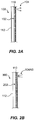
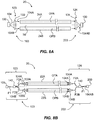
- FIG. 3 is a cross-sectional view of example system 10 that includes an example embodiment of assembly 20.
- Assembly 20 includes a top optical waveguide ("top waveguide”) 22A and a bottom optical waveguide (“bottom waveguide”) 22B.
- Top and bottom waveguides 22A and 22B have respective input edges 23A, 23B adjacent light source 100 and respective output edges 24A and 24B adjacent detector 200.
- the top and bottom waveguides 22A and 22B also have respective bodies 25A and 25B that are substantially transparent to the wavelength of light 104 emitted by light source 100.
- Top and bottom waveguides 22A and 22B also have respective upper surfaces 26A and 26B, and respective lower surfaces 27A and 27B that are defined by respective bodies 28A and 28B.
- the lower surface 27A of top waveguide 22A and the upper surface 26A of lower waveguide 22B are spaced apart by a gap 30.
- gap 30 is filled with a solid material while in another example is filled with air.
- Solid materials may comprise low index, transparent, low modulus, and/or high elasticity materials that have limited absorption of the evanescent wave.
- Gap 30 has a thickness TH 30 that in an example can range from 0 microns (i.e., no gap) to about 2 mm.
- gap 30 is formed by spacers 32. Other thickness TH 30 for gap 30 are possible depending on the particular application for assembly 20.
- top and bottom waveguides 22A and 22B are defined by first and second transparent and generally planar glass sheets.
- materials other than glass can be used, such as polymers, plastics and other non-glass materials that are substantially transparent at the wavelength of light 104.
- System 100 includes an input optical system 123 operably arranged between light source 100 and input edges 23A and 23B of top and bottom waveguides 22A and 22B.
- System 100 also includes an output optical system 124 operably arranged between light source 100 and output edges 24A and 24B of top and bottom waveguides 22A and 22B.
- Input optical system is configured to receive (coherent) light 104 from light source 100 form therefrom collimated (coherent) light beams 104A and 104B, and to direct these light beams into top and bottom waveguides 22A and 22B, respectively.
- Light beams 104A and 104B travel through top and bottom waveguides 22A and 22B over respective optical paths OPA and OPB to output edges 24A and 24B.
- Optical paths OPA and OPB are separate optical paths within top and bottom waveguides respectively, i.e., light beams 104A and 104B do not overlap with each other as they travel through their respective waveguides.
- Output optical system 124 is configured to receive the light beams 104A and 104B that exit respective output edges 24A and 24B and combine the beams so that they interfere, thereby forming an interfered light beam 104AB.
- the interfered light beam 104AB is directed to detector 200, which detects the interfered light beam.
- top and bottom waveguides can have any reasonable configuration that allows them to guide respective light beams 104A and 104B.
- optical paths OPA and OPB represent the lowest-order mode of the top and bottom waveguides 24A and 24B.
- input and output optical systems 123 and 124 can also be referred to as mode conditioners, since they are used to excite and detect a select mode (here, the lowest-order mode) of top and bottom waveguides 24A and 24B.
- the optical paths OPA and OPB represent higher modes or a combination of modes.
- Top and bottom waveguides 22A and 22B may generally be made of any suitably transparent material that can be formed into a thin planar sheet, such as plastic, acrylic, glass, etc., and that supports the transmission of light beams 104A and 104B within their respective bodies 28A and 28B without substantial loss due to scattering or absorption.
- top and bottom waveguides 22A and 22B have thicknesses TH A and TH B such that the waveguides can flex without breaking when pressure is locally applied at top surface 22 at touch location TL.
- An exemplary range for thickness THA is from 0.3 mm to 0.8 mm, and for THB is from 0.3 to 1.5 mm.
- THA is 0.3, 0.4, 0.5, 0.6, 0.7, or 0.8 mm.
- THB is 0.3, 0.4, 0.5, 0.6, 0.7, 0.8, 0.9, 1.0, 1.1, 1.2, 1.3, 1.4, or 1.5 mm.
- Other thickness can be employed consistent with the particular application for touch system 10. In an example, only top waveguide 22A has a thickness that allows it to flex, while bottom waveguide 22B is sufficiently thick or is otherwise rigid that it retains its generally planer configuration even when the top waveguide is subject to a flexing force due to a touch event TE.
- top and bottom waveguides may be formed from a chemically strengthened glass, such as a soda-lime-type glass.
- An example glass for top and bottom waveguides 22A and 22B is an alkali aluminosilicate glass hardened through ion exchange. These types of glass can comprise Na 2 O (soda), CaO (lime) and SiO 2 (silica), but can also include oxides such as MgO, Li 2 O, K 2 O, ZnO, and ZrO 2 . Once hardened through ion exchange, these types of glass exhibit certain characteristics that make them desirable for touch screen applications, as well as other applications (e.g., as a cover glass).
- soda-lime-type glass suitable for use as waveguiding sheets may be found in one or more of U.S. Patent Application No. 11/888,213 filed July 31, 2007 ; U.S. Patent Application No. 12/537,393 filed August 7, 2009 ; U.S. Patent Application No. 12/545,475 filed August 21, 2009 ; and U.S. Patent Application No. 12/392,577 filed February 25, 2009 .
- An exemplary glass for use herein is Gorilla® glass, from Corning, Incorporated, Corning, NY.
- an exemplary glass, such as low-iron Gorilla® glass or other low-iron ion-exchanged glass is transparent to IR-wavelength light 104.
- the configuration of assembly 20 defines an interferometer wherein top and bottom waveguides 22A and 22B define the two different arms of the interferometer over which light 104A and 104B respectively travel.
- interfered light 104AB is formed from light 104A and light 104B that travel through separate (i.e., non-overlapping) optical paths over the two arms of the interferometer.
- the interferometer is configured to be unbalanced so that interference occurs at detector 200. This can be accomplished by making optical paths OPA and OPB different from each other, e.g., by having one of top and bottom waveguides 22A and 22B slightly longer than the other. This introduces an initial or first optical path difference ⁇ OPD 1 .
- optical paths OPA and OPB remain constant so that the first or initial optical path difference ⁇ OPD 1 stays the same.
- a touch event TE occurs on upper surface 26A of top waveguide 22A, it creates a change in the at least one of optical paths OPA and OPB giving rise to a second optical path difference ⁇ OPD 2 that causes a change in the interfered light 104AB detected by detector 200.
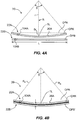
- FIG. 4A is a cross-sectional view of top and bottom waveguides 22A and 22B when upper surface 26A is subject to a touch event TE at a touch event location TL that bends the top waveguide. It is assumed that both the top and bottom waveguides have a length L when no touch event TE is occurring. When a touch event TE occurs at touch location TL, top waveguide 22A bends with a radius of curvature R measured relative to a central longitudinal axis of the top waveguide. This is just one bending scenario and other bending scenarios are discussed below.
- the new optical path OPA' associated with the flexed top waveguide 22A is longer than the optical path OPA of the unflexed top waveguide.
- the optical path OPB of bottom waveguide 22B remains substantially unchanged. This is true whether the bending is over the entire length L of top waveguide 22A or whether the bending is more localized.
- the optical path difference between the optical paths OPA' and OPB of the top and bottom waveguides 22A and 22B which can also be denoted as ⁇ OPD 2 , is about ⁇ r. If ⁇ r is for example about 2.5 microns, that would be roughly equal to two wavelengths of infrared light of wavelength of 800 microns or so. This amount of optical path difference ⁇ OPD 2 , would manifest itself as a change in the interfered light 104AB, e.g., a change in the amount of optical power due to shifting fringes in the detected portion of the resulting interference pattern.
- FIG. 4B is similar to FIG. 4A and illustrates an example of assembly 20 where top and bottom waveguides 22A and 22B are separated by a very thin layer 33 of material so that both waveguides flex when subjected to pressure at touch location TL.
- Top waveguide 22A flexes to have a radius of curvature R A while bottom waveguide 22B flexes to have a radius of curvature R B .
- the optical path difference ⁇ OPD 2 in the optical path lengths OPA' and OPB' associated with the flexed waveguides is approximated by ⁇ (R B -R A ). Again, this is true in the case when the bending of the two waveguides is localized.
- the nominal length L of the top and bottom waveguides 22A and 22B from their respective input ends 23A, 23B to their respective output ends 24A, 24B is about 17 mm. The values of these parameters are all consistent with being able to interferometrically detect the occurrence of a touch event TE.
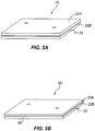
- FIG. 5A is an elevated view of an example assembly 20 showing top waveguide 22A, bottom waveguide 22B with layer 33 in between.
- Layer 33 may be transparent or opaque, or may not be included in assembly 20.
- Layer 33 may be relatively thin or may be sufficiently thick to constitute a support layer or substrate.
- top waveguide 22A is made of a first material having a modulus of elasticity E1 while bottom waveguide 22B is made of a material having a modulus of elasticity E2, wherein E2 ⁇ E1.
- E1 modulus of elasticity
- E2 modulus of elasticity
- This configuration limits the flexing of the combined structure to the location where the force or pressure is applied. Said differently, the radius of curvature of the bending is stronger and more localized.
- FIG. 5B is similar to FIG. 5A and illustrates an embodiment of assembly 20 where top and bottom waveguide 22A and 22B each have a modulus of elasticity E1 and are supported on a support substrate 86 having an elastic modulus E2, wherein E2 ⁇ E1.
- the configuration of FIG. 8B also limits the flexing of the combined structure to the location where the force or pressure is applied, i.e., the radius of curvature of the bending is stronger and more localized.
- top and bottom waveguides 22A and 22B can have a modulus of elasticity E1A and E1B, and the condition E2 ⁇ E1B ⁇ E1A is satisfied.
- FIGS. 5C and 5D are cross-sectional views of an example assembly 20 wherein top waveguide 22A is sufficiently thin and the underlying support substrate 80 or 86 (i.e., a transparent or an opaque support substrate) is sufficiently flexible so that the touch event TE causes a more localized curvature at the touch event location TL.
- finger 50 is shown as causing touch event TE.
- the radii of curvature R A and R B are smaller than in the case where the bending of the top waveguide (or both of the top and bottom waveguides) occurs over a larger distance.
- FIG. 6A is a cross-sectional view of an example embodiment of assembly 20 wherein top and bottom waveguides 22A and 22B are formed in the body 84 of a transparent sheet 80 and have a gradient index.
- the gradient-index top and bottom waveguides are formed using an ion-exchange process.
- the light beams 104A and 104B that respectively travel in top and bottom waveguides 22A and 22B are shown as a fundamental guided mode in each of the gradient-index waveguides.
- FIG. 6B is similar to FIG. 6A and illustrates an example embodiment wherein the top and bottom waveguides 22A and 22B are formed as layered structures on the top and bottom sides of support substrate 86 that has a body 88 that need not be transparent to the operating wavelength of light.
- Top and bottom waveguides 22A and 22B are shown as being formed by a high-index core layer 90 that includes a lower-index cladding layer 92 adjacent the core layer.
- the bulk index of body 88 serves as the cladding layer on the other side of core layer 90.
- support substrate 86 is the same as transparent glass sheet 80.
- support substrate 86 is made of a flexible material such as plastic, acrylic, thin metal, etc. If body 88 is opaque, then the top and bottom waveguides 22A and 22B each require an additional cladding layer 94 adjacent body 88 of support substrate 86, as illustrated in FIG. 6C .
- controller 300 via processor 302 drives the activation of light-source 100 via a light-source signal SL and also controls the detection of interfered light 104AB at detector 200.
- Detector 200 generates detector signal SD in response to detecting interfered light 104AB, wherein the strength of the detector signal SD is representative of the intensity of the detected interfered light.
- Portions of interface circuit 306 can be placed near detector 200. For example, preamplifiers and analog-to-digital converters (not shown) may be placed near detector 200 to eliminate noise that may be induced in long wires between processor 302 and the detectors 200, particularly when the processor is centrally located.
- processor 302 controls the light emission and detection process to optimize the detection of interfered light 104AB, e.g., by providing a characteristic (e.g., a modulation) to the light 104 from the light-source elements 102, or by gating detectors 200 to reduce noise, etc., or both.
- the modulation may be wavelength modulation or intensity modulation.
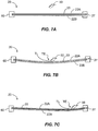
- FIGS. 7A through 7C illustrate an example of how a finger 50 is used to create a touch event TE at a touch location TL, with the touch event causing enough pressure to flex top and bottom waveguides 22A and 22B.
- assembly 20 includes a frame 60 at perimeter 27, wherein the frame supports top and bottom waveguides 22A and 22B as well as layer 33 sandwiched between.
- the flexing of assembly 20 is shown as being gradual. In other embodiment such as those described above in connection with FIGS. 5C and 5D , the bending can be more localized. In an example, the bending can be a combination of localized bending or deformation and a more gradual, larger-scale flexing.
- FIG. 8A is a cross-sectional diagram of an example assembly 20 that illustrates an example configuration for input and output optical systems 123 and 124.
- input and output optical systems include respective lenses 133 and 134, which can each comprise one or more lenses, lens elements, or other optical elements.
- Lens 133 is configured to receive diverging light 104 from light source 100 and form collimated light 104A and 104B.
- lens 134 is designed to receive collimated light beams 104A and 104B and focus them to form interfered light 104AB at detector 200.
- the combination of light source 100 and input optical system 123 defines a light source system 103
- the combination of detector 200 and output optical system 124 defines a detector system 203 (see FIG. 3 ).
- FIG. 8B is similar to FIG. 8A and illustrates an example embodiment where optical fibers are used to configure the input and output optical systems 123 and 124.
- Input optical system 123 includes a first optical fiber section F1 that is optically connected at one end to light source 100 and at the other end to a fiber optic coupler 140.
- Fiber optic coupler 140 is also optically coupled to respective ends of two other optical fiber sections F2A and F2B.
- First and second lenses 133A and 133B are arranged adjacent output ends of optical fiber sections F2A and F2B, respectively.
- Lenses 133A and 133B may each comprise one or more lenses, lens elements, or other optical elements.
- Light 104 from light source 100 is carried to coupler 140 by fiber section F1.
- Coupler 140 serves to split the light between optical fiber sections F2A and F2B so that light beams 104A and 104B respectively travel in these fibers.
- Lenses 133A and 133B are arranged adjacent the output ends of optical fiber sections F2A and F2B and collimate light 104A and 104B and direct the collimated light into respective top and bottom waveguides 22A and 22B.
- output optical system is configured in essentially the same manner but in reverse.
- collimated light beams 104A and 104B from top and bottom waveguides 22A and 22B are received by respective lenses 134A and 134B that focus these light beams into respective optical fiber sections F2A and F2B on the detector side.
- Lenses 134A and 134B may each comprise one or more lenses, lens elements, or other optical elements.
- Light 104A and 104B travels in these fiber sections to coupler 140, where they are combined to form interfered light beam 104AB.
- Interfered light beam 104AB then travels in fiber section F1 from coupler 140 to detector 200, which then detects the interfered light beam.
- Detector 200 is configured to convert the detected interfered light beam 104AB to an electrical signal embodied by detector signal SD, which in an example is a photocurrent.
- the detector may be configured to measure signal via a variety of methods, including overall signal intensity, integrated signal intensity, signal intensity at a particular wavelength, signal frequency, changes in signal frequency, etc.
- the detector electrical signal SD is then sent to processor 302 for processing, as described below. Such processing can be used to extract information relating to changes in the applied pressure at top surface 26A of top waveguide 22A created by touch event TE at touch location TL.
- FIG. 8C is similar to FIG. 8B , except that bottom waveguide 22B is in the form of optical fiber section F2B, which now directly connects the two fiber couplers 140 and serves as the second arm of the interferometer.
- aspects of the disclosure include determining the time-evolution of the touch event TE. This can be used for example to determine a relative amount of pressure that is applied to upper surface 26A of top waveguide 22A by, for example, a finger, a stylus, the eraser-end of a pencil, or like implement. In the discussion below, a finger and a stylus with a compressible end are used by way of non-limiting example to describe the pressure-sensing capabilities of touch system 10. Aspects of the disclosure include detecting respective pressures associated multiple touch events, such as when touch system 10 is used in forming a pressure-sensing keyboard, as discussed below. It is noted here that the pressure applied to assembly 30 at top waveguide 22A may be through another surface that resides atop surface 26A, such as a coating layer.
- FIGS. 9A and 9B are plots of wavelength ⁇ vs. detector optical power ("power") in normalized units in the case where the optical path difference ⁇ OPD 2 between the top and bottom waveguides is 7.5 ⁇ m and 15 ⁇ m, respectively. It can be seen from FIGS. 9A and 9B that the detector signal SD from detector 200 can vary as a sine wave that changes frequency as the optical path difference ⁇ OPD 2 increases. Thus, by monitoring the change in frequency of detector signals SD, one can determine the time-evolution of the deflection in assembly 20 due to a touch event. This time-evolution of the touch event can be used to assess the amount of pressure vs. time being applied to the touch location TL. It can also be used to sense multiple touches in succession, i.e., a double-tap.
- power wavelength ⁇ vs. detector optical power
- light source 100 is wavelength modulated via processor 302 of controller 300 via light source control signal SL (see FIG. 1 ).
- This causes a change in interfered light beam 104AB by changing the optical paths OPA and OPB of light beams 104A and 104B in a select manner.
- This select change manifests itself in detector signal SD, which is processed (filtered) by controller 300 to bring out the laser modulation frequency. This can be accomplished, for example, by a lock-in amplifier.
- the time evolution of the processed detector signal SD is used to characterize the time evolution of touch event TE.
- an object e.g., finger 50, stylus, etc.
- a small amount of flexing of the transparent sheet occurs as an object (e.g., finger 50, stylus, etc.) initially contacts surface 26A of top waveguide 22A.
- the amount of flexing of the top waveguide changes, so that optical path length difference OPD 2 continuously changes.
- the changing optical path lengths show up as a continuous change in the processed detector signal SD.
- the processed detector signal SD stops changing. At this point, the amount of time that the processed detector signal SD remains constant can be measured.
- This information can be used, for example, to carry out a function by requiring the touch event to have associated therewith not only a certain amount of pressure but a select duration as well. Further in the example embodiment, it can be required that the touch event have a select time evolution in pressure that is consistent with say a finger or stylus used to intentionally cause a touch event, as opposed to say an arbitrary object pressing down on the surface 26A of top waveguide 2A and inadvertently triggering a touch event.
- FIGS. 10A and 10B are top-down views of system 10, wherein FIG. 10A shows an example where light beams 104A and 104B travel over respective optical paths OPA and OPB from light source 100 to detector 200 in top and bottom waveguides (not shown) of assembly 20. Only a single light source element 102 and detector element 202 are shown in FIG. 10A , while an extended light source and an extended detector 200 are shown in FIG. 10B .
- FIG. 10B shows a keyboard 70 that includes indicia denoting for example the usual typing keyboard keys 72.
- the close-up inset view of key "F" shows that the key area is optionally provided with surface roughness denoted 29 that increases the amount of light scattering for the keys, particularly when they are pressed down upon with a finger to create a touch event.
- This may be used to illuminate keys 72 using guided light 104A. While guided light 104 travels straight down top waveguide 22A, the light therein interacts with upper surface 26A. If this surface is smooth, then there is very little if any loss from scattering. The introduction of surface roughness 29 will allow guided light 104A to interact with select portions of upper surface 26A and allow some of this light to escape and be visible to a viewer or user of the keyboard.
- FIG. 11A is a cross-sectional view of an example dual-core optical fiber 320 that includes two optical fiber cores 322A and 322B embedded in a cladding 323.
- FIG. 11B is a cross-sectional view of a fiber assembly 330 that has two optical fibers 320A and 320B disposed adjacent one another and that include respective cores 322A and 322B surrounded by respective claddings 323A and 323B.
- cores 322A and 322B are formed such that they support just a single mode at the operating wavelength of the dual-core optical fiber.
- Optical fibers such as dual-core fiber (“fiber") 320, fiber assembly 300 or like optical fiber configurations can be used to form a Mach-Zehnder interferometer. Examples of such interferometers are disclosed in USP 5,295,205 , USP 5,943,458 , USP 5,351,325 and USP 6,862,396 .
- FIG. 12 is taken from FIG. 1 of the '458 patent and illustrates an example fiber-based interferometer that includes a pair of fibers F 1 and F 2 . The fibers are coupled to one another for light transfer therebetween at a first coupler C 1 and a second couple C 2 . The couplers are arranged to transfer light, one fiber to the other.
- Couplers C 1 and C 2 may be so-called “evanescent" couplers in which narrowed, elongated portions of the fibers are closely juxtaposed with one another within a matrix or outer coating.
- the couplers may be 3dB couplers, arranged to transfer approximately one-half of the optical power supplied on one fiber to the other fiber.
- Fibers F 1 and F 2 have phase-shift regions with different optical path lengths disposed between the couplers.
- the optical path length over the phase shift region in fiber F 1 is different from the optical path length over the phase shift region in fiber F 2 .
- the optical path length difference has been provided either by making the phase shift region of one fiber physically longer than the other, or by making the two fibers F 1 and F 2 with different propagation constants so that the velocity of light within the two fibers is different.
- the latter structure can be achieved by making the fibers with different refractive index profiles.
- the fibers are "step-index" fibers, incorporating a core having a relatively high refractive index and a coating with a relatively low refractive index overlying the core
- the two fibers may have cores of different refractive indices, different core diameters, different coating refractive indices or some combination of these.
- the single stage Mach-Zehnder filter depicted in FIG. 12 will direct light supplied through input 1 either to output 3 or to output 4 depending upon the wavelength of the light.
- More complex Mach-Zehnder devices utilize multiple stages with multiple phase shift regions and multiple couplers connected in series to achieve certain desirable wavelength-selective characteristics.
- Still other Mach-Zehnder devices incorporate more than two fibers connected in parallel between the couplers, as described in the aforementioned USP 5,351,325 .
- Various optical fibers incorporate different optical path lengths. Desirably, the optical path length differences are selected to provide optical path length differences that are rational or integral multiples of one another.
- "OPLD" can also represent the optical path length difference that arises due to a touch event TE, as explained below.
- a light source element 102 (and input optical system 123) is optically coupled into one of input 1 or 2
- detector element 202 (and output optical system 124) is provided at one of output 3 and 4.
- first and second detector elements 202 and corresponding output optical systems 124 can be placed at outputs 3 and 4 respectively to better detect interfered light 104AB.
- the amount of interfered light 104AB being outputted at ends 3 and 4 can vary, so it can be more accurate to measure the amount of power in both of these output ends to ensure an accurate measurement of the optical path difference ⁇ OPD 2 caused by a touch event TE.
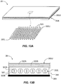
- FIG. 13A is an elevated view of an example assembly 20 that includes upper and lower arrays 350U and 350L of optical fibers 320 that form an optical fiber detection grid, as shown in the close-up view.
- This grid configuration can be used for (x,y) detection of the touch location TL of touch event since at a given touch location, the optical paths differences between cores 322A and 322B will change in relation to their proximity to the touch location.
- the (x,y) characteristics of the interference effects can be determined by processing the corresponding detector signals SD.
- FIG. 13B is a close-up cross-sectional view of the example assembly 20 of FIG. 13A .
- upper and lower fiber arrays 350U and 350L are supported in a layer 354 of support material of relatively low elastic modulus such as polyimide, which has an elastic modulus about 20 times less than that of glass.
- Assembly 20 also includes a substrate 360 that supports the support material 354 and the upper and lower fiber arrays 350U and 350L.
- FIG. 14A is a cross-sectional view of one of fibers 320 in upper fiber array 322A, and showing finger 50 just about the fiber.
- FIG. 14B is similar to FIG. 14A , but shows finger 50 pressing down on fiber 320 to form touch event TE at touch location TL. Because fiber 320 is supported in a manner that allows it to flex as part of the optical fiber grid formed by top and bottom fiber arrays 350T and 350L. Because of the bending of fiber 320, the length of optical paths OPA and OPB for light 104A and 104B traveling in cores 322A and 322B change by different amounts, thereby creating an optical path difference ⁇ OPD 2 in the same manner as the planar versions of top and bottom waveguides 22A and 22B.
- FIG. 14C is similar to FIG. 14B and illustrates an example embodiment where the bending of fiber 320 is more localized at the touch location TL based on the construction of the fiber.
- fiber 320 may be made of more flexible materials than a conventional dual-core optical fiber.
- Touch system 10 can be used in combination with conventional position-sensing display systems, such as those that are capacitive-based and resistive-based.
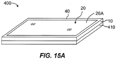
- FIG. 15A is a schematic elevated view of an example pressure-sensing display 400 formed by operably arranging touch system 10 adjacent and above (e.g., atop) a conventional display unit 410, such as a liquid crystal display, which display may have conventional position-based sensing capability.
- a conventional display unit 410 such as a liquid crystal display, which display may have conventional position-based sensing capability.
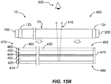
- FIG. 15B is a schematic cross-sectional, partial exploded view of an example touch-sensitive display 400 illustrating an example of how to integrate touch system 10 with conventional display unit 410.
- the conventional display unit 410 is shown in the form of a liquid crystal display that includes a backlighting unit 414 that emits light 416, a thin-film transistor (TFT) glass layer 420, a liquid crystal layer 430, a color filter glass layer 450 with a top surface 452, and a top polarizer layer 460 with a top surface 462, all arranged as shown.
- a frame 470 is disposed around the edge of color filter glass layer 450.
- Light source 100 is shown by way of example as being operably supported within frame 470. This forms an integrated display assembly 480 having a top side 482.
- assembly 20 is added to integrated display assembly 480 of conventional display unit 410 by operably disposing the assembly on top side 482.
- the assembly 20 can include the aforementioned cover 40 in the form of an IR-transparent but visibly opaque layer disposed adjacent light source 100 and detector 200.
- various indicia or indicium such as keyboard 70 (see FIG. 8B ) may be presented to user 500 on or through top surface 26A to guide the user to interact with touch system 10.
- the indicium may include areas on top surface 22 of transparent sheet 20 that are set aside for indicating user choices, software execution, etc., or to indicate a region where the user should create touch event TE. Such region, for example, might be required where light 104 does not reach certain portions of top surface 26A.
Landscapes
- Engineering & Computer Science (AREA)
- General Engineering & Computer Science (AREA)
- Theoretical Computer Science (AREA)
- Human Computer Interaction (AREA)
- Physics & Mathematics (AREA)
- General Physics & Mathematics (AREA)
- Optical Integrated Circuits (AREA)
Applications Claiming Priority (3)
| Application Number | Priority Date | Filing Date | Title |
|---|---|---|---|
| US201261651136P | 2012-05-24 | 2012-05-24 | |
| EP13726376.0A EP2856290B1 (de) | 2012-05-24 | 2013-05-21 | Wellenleiterbasiertes berührungssystem mit interferenzeffekten |
| PCT/US2013/041939 WO2013177107A1 (en) | 2012-05-24 | 2013-05-21 | Waveguide-based touch system employing interference effects |
Related Parent Applications (2)
| Application Number | Title | Priority Date | Filing Date |
|---|---|---|---|
| EP13726376.0A Division-Into EP2856290B1 (de) | 2012-05-24 | 2013-05-21 | Wellenleiterbasiertes berührungssystem mit interferenzeffekten |
| EP13726376.0A Division EP2856290B1 (de) | 2012-05-24 | 2013-05-21 | Wellenleiterbasiertes berührungssystem mit interferenzeffekten |
Publications (1)
| Publication Number | Publication Date |
|---|---|
| EP3617858A1 true EP3617858A1 (de) | 2020-03-04 |
Family
ID=48539426
Family Applications (2)
| Application Number | Title | Priority Date | Filing Date |
|---|---|---|---|
| EP13726376.0A Active EP2856290B1 (de) | 2012-05-24 | 2013-05-21 | Wellenleiterbasiertes berührungssystem mit interferenzeffekten |
| EP19202661.5A Withdrawn EP3617858A1 (de) | 2012-05-24 | 2013-05-21 | Wellenleiterbasiertes berührungssystem mit interferenzeffekten |
Family Applications Before (1)
| Application Number | Title | Priority Date | Filing Date |
|---|---|---|---|
| EP13726376.0A Active EP2856290B1 (de) | 2012-05-24 | 2013-05-21 | Wellenleiterbasiertes berührungssystem mit interferenzeffekten |
Country Status (5)
| Country | Link |
|---|---|
| US (2) | US9952719B2 (de) |
| EP (2) | EP2856290B1 (de) |
| CN (1) | CN104641330B (de) |
| TW (1) | TWI609311B (de) |
| WO (1) | WO2013177107A1 (de) |
Families Citing this family (25)
| Publication number | Priority date | Publication date | Assignee | Title |
|---|---|---|---|---|
| US9285623B2 (en) * | 2012-10-04 | 2016-03-15 | Corning Incorporated | Touch screen systems with interface layer |
| US9902644B2 (en) | 2014-06-19 | 2018-02-27 | Corning Incorporated | Aluminosilicate glasses |
| JP2016058014A (ja) * | 2014-09-12 | 2016-04-21 | 日東電工株式会社 | 位置センサ |
| CN106155399B (zh) * | 2015-04-24 | 2023-05-16 | 宸鸿科技(厦门)有限公司 | 触控装置 |
| US10310674B2 (en) * | 2015-07-22 | 2019-06-04 | Semiconductor Components Industries, Llc | Optical touch screen system using radiation pattern sensing and method therefor |
| US11788869B2 (en) | 2016-02-25 | 2023-10-17 | Cornell University | Waveguides for use in sensors or displays |
| CA3015906A1 (en) * | 2016-02-25 | 2017-08-31 | Cornell University | Waveguides for use in sensors or displays |
| US10043050B2 (en) * | 2016-03-07 | 2018-08-07 | Microsoft Technology Licensing, Llc | Image sensing with a display |
| CN106293266B (zh) * | 2016-07-27 | 2019-02-12 | 京东方科技集团股份有限公司 | 一种触控模组和显示装置 |
| CN106293241B (zh) * | 2016-08-17 | 2019-01-04 | 京东方科技集团股份有限公司 | 一种压力传感器及显示装置 |
| KR102495467B1 (ko) | 2016-12-07 | 2023-02-06 | 플라트프로그 라보라토리즈 에이비 | 개선된 터치 장치 |
| FI3717944T3 (fi) * | 2017-11-29 | 2025-09-04 | Univ Cornell | Aaltoputki ja samaan perustuvia antureita |
| CN112747847B (zh) * | 2018-07-02 | 2021-10-15 | 上海交通大学 | 光波导压力测量系统 |
| EP3667279B1 (de) * | 2018-12-10 | 2021-12-01 | FRAUNHOFER-GESELLSCHAFT zur Förderung der angewandten Forschung e.V. | Sensoreinrichtung |
| CN110083274B (zh) * | 2019-04-28 | 2022-05-06 | 业成科技(成都)有限公司 | 光学触控装置及其系统 |
| CN110442273A (zh) * | 2019-07-19 | 2019-11-12 | 深圳市华星光电半导体显示技术有限公司 | 红外触控显示装置 |
| CN110427114A (zh) * | 2019-08-01 | 2019-11-08 | 京东方科技集团股份有限公司 | 输入设备以及电子终端组件 |
| CN114730228A (zh) * | 2019-11-25 | 2022-07-08 | 平蛙实验室股份公司 | 一种触摸感应设备 |
| CN111157154B (zh) * | 2020-01-07 | 2021-04-09 | 腾讯科技(深圳)有限公司 | 触觉传感器、触碰事件的检测方法、装置及智能机器人 |
| CN111256889B (zh) * | 2020-01-07 | 2021-05-04 | 腾讯科技(深圳)有限公司 | 触觉传感器、触觉事件的检测方法、装置及智能机器人 |
| CN110823427B (zh) * | 2020-01-09 | 2020-04-14 | 腾讯科技(深圳)有限公司 | 触觉传感器、压力事件的检测方法、装置及智能机器人 |
| CN112558807B (zh) * | 2020-11-12 | 2024-06-28 | 周幼宁 | 一种智能表面 |
| CN113157127B (zh) * | 2021-02-04 | 2024-11-05 | 识瓴电子科技(南通)有限责任公司 | 智能表面系统集成的方法 |
| WO2022246807A1 (en) * | 2021-05-28 | 2022-12-01 | Huawei Technologies Co., Ltd. | Electronic apparatus comprising haptic feedback arrangement and method of providing such feedback |
| US20250377734A1 (en) * | 2024-06-11 | 2025-12-11 | Apple Inc. | Input system for portable electronic device |
Citations (8)
| Publication number | Priority date | Publication date | Assignee | Title |
|---|---|---|---|---|
| US4733068A (en) * | 1986-04-07 | 1988-03-22 | Rockwell International Corporation | Crossed fiber optic tactile sensor |
| US5295205A (en) | 1993-03-29 | 1994-03-15 | Corning Incorporated | Environmentally stable monolithic Mach-Zehnder device |
| US5351325A (en) | 1993-04-29 | 1994-09-27 | Corning Incorporated | Narrow band Mach-Zehnder filter |
| US5943458A (en) | 1995-06-09 | 1999-08-24 | Corning Incorporated | Mach-Zehnder interferometric devices with composite fibers |
| DE10139147A1 (de) * | 2001-08-09 | 2003-03-06 | Siemens Ag | Verfahren und Vorrichtung zur Störung eines optischen Vorgangs an einem optischen Touchscreen |
| US6862396B2 (en) | 1999-11-02 | 2005-03-01 | Georgia Tech Research Corporation | Apparatus and method of optical transfer and control in plasmon supporting metal nanostructures |
| US20110122091A1 (en) | 2009-11-25 | 2011-05-26 | King Jeffrey S | Methods and apparatus for sensing touch events on a display |
| EP2437145A1 (de) * | 2010-09-17 | 2012-04-04 | Research In Motion Limited | Berührungsempfindliche Anzeige mit Druckerkennung und Verfahren |
Family Cites Families (121)
| Publication number | Priority date | Publication date | Assignee | Title |
|---|---|---|---|---|
| US3673327A (en) | 1970-11-02 | 1972-06-27 | Atomic Energy Commission | Touch actuable data input panel assembly |
| US4484179A (en) | 1980-04-16 | 1984-11-20 | At&T Bell Laboratories | Touch position sensitive surface |
| US4542375A (en) | 1982-02-11 | 1985-09-17 | At&T Bell Laboratories | Deformable touch sensitive surface |
| WO1983003314A1 (en) | 1982-03-16 | 1983-09-29 | Burroughs Corp | Fiber wrap keyboard and switch |
| US4511760A (en) | 1983-05-23 | 1985-04-16 | International Business Machines Corporation | Force sensing data input device responding to the release of pressure force |
| US4725978A (en) | 1983-05-30 | 1988-02-16 | Ichiro Fujioka | Graphic pattern inputting apparatus |
| US4710760A (en) | 1985-03-07 | 1987-12-01 | American Telephone And Telegraph Company, At&T Information Systems Inc. | Photoelastic touch-sensitive screen |
| US4687885A (en) | 1985-03-11 | 1987-08-18 | Elographics, Inc. | Electrographic touch sensor with Z-axis capability |
| US5222400A (en) | 1985-12-18 | 1993-06-29 | Spaceball Technologies Incorporated | Force and torque converter |
| CA1294802C (en) | 1986-06-04 | 1992-01-28 | Benjamin J. Ainslie | Optical waveguides and their manufacture |
| US4834480A (en) | 1988-04-21 | 1989-05-30 | Bell Communications Research, Inc. | Composite channel waveguides |
| FI82989C (fi) | 1989-04-13 | 1991-05-10 | Nokia Oy Ab | Foerfarande foer framstaellning av en ljusvaogledare. |
| JPH0377222A (ja) | 1989-08-17 | 1991-04-02 | Sony Corp | 入力装置 |
| US5610629A (en) | 1991-12-06 | 1997-03-11 | Ncr Corporation | Pen input to liquid crystal display |
| US5712937A (en) | 1994-12-01 | 1998-01-27 | Asawa; Charles K. | Optical waveguide including singlemode waveguide channels coupled to a multimode fiber |
| GB2313195A (en) | 1996-05-02 | 1997-11-19 | Univ Bristol | Data entry device |
| JPH10207616A (ja) | 1997-01-20 | 1998-08-07 | Sharp Corp | 入力装置 |
| US6031520A (en) | 1997-04-04 | 2000-02-29 | De Gotari; Sergio Salinas | Substantially stationary pressure sensitive system for providing input to an electrical device, particularly a computer |
| GB2329020B (en) | 1997-09-04 | 2003-04-23 | Delco Electronics Europ Gmbh | Electrically operable device operation |
| US6556149B1 (en) | 1999-03-01 | 2003-04-29 | Canpolar East Inc. | Switches and joysticks using a non-electrical deformable pressure sensor |
| US6737591B1 (en) | 1999-05-25 | 2004-05-18 | Silverbrook Research Pty Ltd | Orientation sensing device |
| CA2273113A1 (en) | 1999-05-26 | 2000-11-26 | Tactex Controls Inc. | Touch pad using a non-electrical deformable pressure sensor |
| US6504530B1 (en) | 1999-09-07 | 2003-01-07 | Elo Touchsystems, Inc. | Touch confirming touchscreen utilizing plural touch sensors |
| US7157649B2 (en) | 1999-12-23 | 2007-01-02 | New Transducers Limited | Contact sensitive device |
| JP2004534974A (ja) | 2000-10-27 | 2004-11-18 | エロ・タッチシステムズ・インコーポレイテッド | 複数のタッチセンサを利用した接触確認式タッチスクリーン |
| KR20010096633A (ko) | 2001-04-18 | 2001-11-08 | 장광식 정윤철 | 도광판 일체형 터치 패널 및 그 적층방법 |
| CA2353697A1 (en) | 2001-07-24 | 2003-01-24 | Tactex Controls Inc. | Touch sensitive membrane |
| JP2005505075A (ja) | 2001-10-09 | 2005-02-17 | コーニンクレッカ フィリップス エレクトロニクス エヌ ヴィ | タッチセンシティビティ機能を有する装置 |
| DE10158775B4 (de) | 2001-11-30 | 2004-05-06 | 3Dconnexion Gmbh | Anordnung zum Erfassen von Relativbewegungen oder Relativpositionen zweier Objekte |
| US6900795B1 (en) | 2002-02-27 | 2005-05-31 | Knight, Iii Jack | Unitary molded lens filter for touch screen interface |
| US20040040800A1 (en) | 2002-07-31 | 2004-03-04 | George Anastas | System and method for providing passive haptic feedback |
| US9195344B2 (en) | 2002-12-10 | 2015-11-24 | Neonode Inc. | Optical surface using a reflected image for determining three-dimensional position information |
| US7685538B2 (en) | 2003-01-31 | 2010-03-23 | Wacom Co., Ltd. | Method of triggering functions in a computer application using a digitizer having a stylus and a digitizer system |
| US7442914B2 (en) | 2003-09-12 | 2008-10-28 | Flatfrog Laboratories Ab | System and method of determining a position of a radiation emitting element |
| CN1867881B (zh) | 2003-09-12 | 2010-08-18 | 平蛙实验室股份公司 | 确定辐射散射/反射件的位置的系统和方法 |
| KR101098635B1 (ko) | 2004-02-13 | 2011-12-23 | 큐알쥐 리미티드 | 정전용량 센서 |
| US7042371B2 (en) | 2004-02-24 | 2006-05-09 | Nokia Corporation | Optical keyboard with geodesic optical elements |
| US7158054B2 (en) | 2004-09-21 | 2007-01-02 | Nokia Corporation | General purpose input board for a touch actuation |
| US7417627B2 (en) | 2004-10-27 | 2008-08-26 | Eastman Kodak Company | Sensing display |
| US8599140B2 (en) | 2004-11-17 | 2013-12-03 | International Business Machines Corporation | Providing a frustrated total internal reflection touch interface |
| US8130210B2 (en) | 2004-11-30 | 2012-03-06 | Avago Technologies Ecbu Ip (Singapore) Pte. Ltd. | Touch input system using light guides |
| US7903090B2 (en) | 2005-06-10 | 2011-03-08 | Qsi Corporation | Force-based input device |
| CN101000529B (zh) | 2006-01-13 | 2011-09-14 | 北京汇冠新技术股份有限公司 | 一种用于红外触摸屏的触摸力检测装置 |
| US7951583B2 (en) | 2006-03-10 | 2011-05-31 | Plc Diagnostics, Inc. | Optical scanning system |
| KR20090007776A (ko) | 2006-05-01 | 2009-01-20 | 알피오 피티와이 리미티드 | 광학 터치스크린용 도파로 물질 |
| US8144271B2 (en) | 2006-08-03 | 2012-03-27 | Perceptive Pixel Inc. | Multi-touch sensing through frustrated total internal reflection |
| KR100917582B1 (ko) | 2006-08-10 | 2009-09-15 | 주식회사 엘지화학 | 비접촉식 좌표입력 시스템용 도광판을 이용한 비접촉식좌표입력 방법 |
| US7920124B2 (en) | 2006-08-29 | 2011-04-05 | Canon Kabushiki Kaisha | Force sense presentation device, mixed reality system, information processing method, and information processing apparatus |
| TWI355631B (en) | 2006-08-31 | 2012-01-01 | Au Optronics Corp | Liquid crystal display with a liquid crystal touch |
| JP4294668B2 (ja) | 2006-09-14 | 2009-07-15 | 株式会社日立製作所 | 点図ディスプレイ装置 |
| WO2008034184A1 (en) * | 2006-09-22 | 2008-03-27 | Rpo Pty Limited | Waveguide configurations for optical touch systems |
| WO2008045207A2 (en) | 2006-10-06 | 2008-04-17 | Qualcomm Mems Technologies, Inc. | Light guide |
| US20080088600A1 (en) | 2006-10-11 | 2008-04-17 | Apple Inc. | Method and apparatus for implementing multiple push buttons in a user input device |
| US20080088597A1 (en) | 2006-10-11 | 2008-04-17 | Apple Inc. | Sensor configurations in a user input device |
| KR101385969B1 (ko) | 2007-03-21 | 2014-04-17 | 삼성전자주식회사 | 화상형성장치 |
| FR2914756B1 (fr) | 2007-04-05 | 2012-09-21 | Jazzmutant | Capteur multi-tactile transparent. |
| US7666511B2 (en) | 2007-05-18 | 2010-02-23 | Corning Incorporated | Down-drawable, chemically strengthened glass for cover plate |
| WO2008147917A2 (en) | 2007-05-22 | 2008-12-04 | Qsi Corporation | Touch-based input device with boundary defining a void |
| US8917244B2 (en) | 2007-06-11 | 2014-12-23 | Honeywell Internation Inc. | Stimuli sensitive display screen with multiple detect modes |
| EP2034287A1 (de) | 2007-09-10 | 2009-03-11 | Nederlandse Organisatie voor Toegepast-Natuuurwetenschappelijk Onderzoek TNO | Optischer Sensor zur Messung einer Kraftverteilung |
| US20090124024A1 (en) | 2007-11-07 | 2009-05-14 | Shingo Kasai | Optical-waveguide sensor chip, method of manufacturing the same, method of measuring substance, substance-measuring kit and optical-waveguide sensor |
| JP4904249B2 (ja) | 2007-11-15 | 2012-03-28 | 日東電工株式会社 | タッチパネル用光導波路およびそれを用いたタッチパネル |
| JP2011507108A (ja) | 2007-12-11 | 2011-03-03 | スキッフ・エルエルシー | タッチ感応被照射ディスプレイ装置およびその操作方法 |
| TWI380196B (en) | 2007-12-25 | 2012-12-21 | Pixart Imaging Inc | Method for detecting users' pressing action and optical operating unit |
| US8179375B2 (en) | 2008-01-04 | 2012-05-15 | Tactus Technology | User interface system and method |
| US8947383B2 (en) | 2008-01-04 | 2015-02-03 | Tactus Technology, Inc. | User interface system and method |
| CN101980983B (zh) | 2008-02-26 | 2014-04-16 | 康宁股份有限公司 | 用于硅酸盐玻璃的澄清剂 |
| US20090219253A1 (en) | 2008-02-29 | 2009-09-03 | Microsoft Corporation | Interactive Surface Computer with Switchable Diffuser |
| US8553014B2 (en) | 2008-06-19 | 2013-10-08 | Neonode Inc. | Optical touch screen systems using total internal reflection |
| US20100001978A1 (en) | 2008-07-02 | 2010-01-07 | Stephen Brian Lynch | Ambient light interference reduction for optical input devices |
| JP5670901B2 (ja) | 2008-08-08 | 2015-02-18 | コーニング インコーポレイテッド | 強化ガラス物品およびその製造方法 |
| JP2012500177A (ja) | 2008-08-21 | 2012-01-05 | コーニング インコーポレイテッド | 電子装置のための耐久性ガラスハウジング/エンクロージャ |
| US8777099B2 (en) | 2008-08-29 | 2014-07-15 | The Invention Science Fund I, Llc | Bendable electronic device status information system and method |
| KR101482125B1 (ko) | 2008-09-09 | 2015-01-13 | 엘지전자 주식회사 | 휴대 단말기 및 그 동작방법 |
| US10289199B2 (en) | 2008-09-29 | 2019-05-14 | Apple Inc. | Haptic feedback system |
| US20100103140A1 (en) | 2008-10-27 | 2010-04-29 | Sony Ericsson Mobile Communications Ab | Touch sensitive device using optical gratings |
| CN101739170A (zh) | 2008-11-12 | 2010-06-16 | 鸿富锦精密工业(深圳)有限公司 | 触控面板组件及触控面板系统 |
| WO2010063320A1 (en) | 2008-12-03 | 2010-06-10 | Agc Flat Glass Europe Sa | Panel of glass comprising at least a sheet of glass, an exciter and a touch sensing device |
| KR101521096B1 (ko) | 2008-12-19 | 2015-05-18 | 삼성디스플레이 주식회사 | 표시장치 |
| JP5239835B2 (ja) * | 2008-12-24 | 2013-07-17 | 富士ゼロックス株式会社 | 光導波路及び光導波路型タッチパネル |
| US8384682B2 (en) | 2009-01-08 | 2013-02-26 | Industrial Technology Research Institute | Optical interactive panel and display system with optical interactive panel |
| CN102388354A (zh) | 2009-02-17 | 2012-03-21 | 诺亚·安格林 | 漂浮平面触摸检测系统 |
| CN101539815A (zh) | 2009-02-25 | 2009-09-23 | 韩鼎楠 | 多点触摸屏操作工具 |
| KR20100102774A (ko) | 2009-03-12 | 2010-09-27 | 삼성전자주식회사 | 터치 감지 시스템 및 이를 채용한 디스플레이 장치 |
| US20100245288A1 (en) | 2009-03-29 | 2010-09-30 | Harris Technology, Llc | Touch Tunnels |
| US8253712B2 (en) | 2009-05-01 | 2012-08-28 | Sony Ericsson Mobile Communications Ab | Methods of operating electronic devices including touch sensitive interfaces using force/deflection sensing and related devices and computer program products |
| US8624853B2 (en) * | 2009-06-01 | 2014-01-07 | Perceptive Pixel Inc. | Structure-augmented touch sensing with frustated total internal reflection |
| US20110032214A1 (en) | 2009-06-01 | 2011-02-10 | Qualcomm Mems Technologies, Inc. | Front light based optical touch screen |
| US20100309169A1 (en) | 2009-06-03 | 2010-12-09 | Lumio Inc. | Optical Touch Screen with Reflectors |
| WO2010146580A1 (en) | 2009-06-14 | 2010-12-23 | Micropointing Ltd. | Finger-operated input device |
| KR101071672B1 (ko) | 2009-06-23 | 2011-10-11 | 한국표준과학연구원 | 접촉힘 세기 또는 압력 세기를 감지하는 촉각센서가 구비된 조도 조절 가능한 전계 발광 소자, 이를 포함하는 평판표시장치, 이를 포함하는 휴대기기 키패드 |
| TWI398804B (zh) | 2009-06-30 | 2013-06-11 | Pixart Imaging Inc | 光學觸控螢幕之位移偵測系統及其方法 |
| CN101957693B (zh) | 2009-07-20 | 2013-04-24 | 鸿富锦精密工业(深圳)有限公司 | 触控系统 |
| US8390481B2 (en) | 2009-08-17 | 2013-03-05 | Apple Inc. | Sensing capacitance changes of a housing of an electronic device |
| JP2013506213A (ja) | 2009-09-30 | 2013-02-21 | ベイジン アイルタッチ システムズ カンパニー,リミティド | タッチスクリーン、タッチシステム及びタッチシステムにおけるタッチオブジェクトの位置決定方法 |
| JP4932895B2 (ja) | 2009-11-12 | 2012-05-16 | 奇美電子股▲ふん▼有限公司 | ディスプレイ装置及び電子機器 |
| US8570297B2 (en) | 2009-12-14 | 2013-10-29 | Synaptics Incorporated | System and method for measuring individual force in multi-object sensing |
| CN101751186B (zh) | 2009-12-30 | 2011-12-21 | 鸿富锦精密工业(深圳)有限公司 | 触摸电子装置及其控制方法 |
| US8368677B2 (en) | 2010-03-31 | 2013-02-05 | Casio Computer Co., Ltd. | Optical sensor device, display apparatus, and method for driving optical sensor device |
| US20120326981A1 (en) | 2010-05-12 | 2012-12-27 | Nec Corporation | Information processing terminal, terminal operation method and computer-readable medium |
| IT1400420B1 (it) | 2010-06-04 | 2013-05-31 | Maria De | Sensore per la misura di una forza esterna applicata a detto sensore. |
| FR2963839B1 (fr) | 2010-08-13 | 2012-08-17 | Delphi Tech Inc | Panneau de commande comportant une touche resistive |
| JP5819965B2 (ja) | 2010-08-27 | 2015-11-24 | インテル・コーポレーション | システム及び装置 |
| US9223431B2 (en) * | 2010-09-17 | 2015-12-29 | Blackberry Limited | Touch-sensitive display with depression detection and method |
| EP2439619B1 (de) | 2010-09-17 | 2019-07-17 | BlackBerry Limited | Berührungsempfindliche Anzeige mit optischem Sensor und Verfahren |
| US20120068939A1 (en) * | 2010-09-17 | 2012-03-22 | Nigel Patrick Pemberton-Pigott | Touch-sensitive display with depression detection and method |
| EP2437144B1 (de) | 2010-09-17 | 2018-08-29 | BlackBerry Limited | Berührungsempfindliche Anzeige mit optischem Sensor und Verfahren |
| US9513737B2 (en) | 2010-09-17 | 2016-12-06 | Blackberry Limited | Touch-sensitive display with optical sensor and method |
| US20120071206A1 (en) | 2010-09-17 | 2012-03-22 | Nigel Patrick Pemberton-Pigott | Touch-sensitive display with optical sensor and method |
| EP2439620B1 (de) | 2010-09-17 | 2018-04-11 | BlackBerry Limited | Berührungsempfindliche Anzeige mit Druckerkennung und Verfahren |
| TWI428804B (zh) | 2010-10-20 | 2014-03-01 | Pixart Imaging Inc | 光學觸控系統及其感測方法 |
| US9235303B2 (en) | 2010-12-20 | 2016-01-12 | Intel Corporation | Micro deflectors on touch sensor |
| US8665244B2 (en) | 2011-02-22 | 2014-03-04 | Microsoft Corporation | Optical touch detection |
| WO2013029641A1 (en) | 2011-08-31 | 2013-03-07 | Sony Ericsson Mobile Communications Ab | Method for operating a touch sensitive user interface |
| EP2748695B1 (de) | 2011-09-16 | 2019-01-02 | Sony Mobile Communications Inc. | Kraftempfindlicher berührungssensor |
| WO2013068651A2 (en) | 2011-11-11 | 2013-05-16 | Qitec Ltd | A touch sensitive operation interface |
| US8994694B2 (en) | 2011-11-30 | 2015-03-31 | Blackberry Limited | Optical interference based user input device |
| US8982084B2 (en) | 2011-12-16 | 2015-03-17 | Flatfrog Laboratories Ab | Tracking objects on a touch surface |
| TWM436872U (en) | 2012-03-15 | 2012-09-01 | Univ China Sci & Tech | Improved optical touch panel including optic fiber for transmission |
| US9405382B2 (en) | 2012-07-24 | 2016-08-02 | Rapt Ip Limited | Augmented optical waveguide for use in an optical touch sensitive device |
| US9041690B2 (en) | 2012-08-06 | 2015-05-26 | Qualcomm Mems Technologies, Inc. | Channel waveguide system for sensing touch and/or gesture |
-
2013
- 2013-04-22 US US13/867,417 patent/US9952719B2/en active Active
- 2013-05-21 EP EP13726376.0A patent/EP2856290B1/de active Active
- 2013-05-21 CN CN201380027193.3A patent/CN104641330B/zh not_active Expired - Fee Related
- 2013-05-21 EP EP19202661.5A patent/EP3617858A1/de not_active Withdrawn
- 2013-05-21 WO PCT/US2013/041939 patent/WO2013177107A1/en not_active Ceased
- 2013-05-22 TW TW102118090A patent/TWI609311B/zh not_active IP Right Cessation
-
2018
- 2018-03-09 US US15/916,924 patent/US10572071B2/en not_active Expired - Fee Related
Patent Citations (8)
| Publication number | Priority date | Publication date | Assignee | Title |
|---|---|---|---|---|
| US4733068A (en) * | 1986-04-07 | 1988-03-22 | Rockwell International Corporation | Crossed fiber optic tactile sensor |
| US5295205A (en) | 1993-03-29 | 1994-03-15 | Corning Incorporated | Environmentally stable monolithic Mach-Zehnder device |
| US5351325A (en) | 1993-04-29 | 1994-09-27 | Corning Incorporated | Narrow band Mach-Zehnder filter |
| US5943458A (en) | 1995-06-09 | 1999-08-24 | Corning Incorporated | Mach-Zehnder interferometric devices with composite fibers |
| US6862396B2 (en) | 1999-11-02 | 2005-03-01 | Georgia Tech Research Corporation | Apparatus and method of optical transfer and control in plasmon supporting metal nanostructures |
| DE10139147A1 (de) * | 2001-08-09 | 2003-03-06 | Siemens Ag | Verfahren und Vorrichtung zur Störung eines optischen Vorgangs an einem optischen Touchscreen |
| US20110122091A1 (en) | 2009-11-25 | 2011-05-26 | King Jeffrey S | Methods and apparatus for sensing touch events on a display |
| EP2437145A1 (de) * | 2010-09-17 | 2012-04-04 | Research In Motion Limited | Berührungsempfindliche Anzeige mit Druckerkennung und Verfahren |
Also Published As
| Publication number | Publication date |
|---|---|
| US10572071B2 (en) | 2020-02-25 |
| EP2856290B1 (de) | 2019-11-27 |
| WO2013177107A1 (en) | 2013-11-28 |
| US20180196577A1 (en) | 2018-07-12 |
| TWI609311B (zh) | 2017-12-21 |
| US20130314368A1 (en) | 2013-11-28 |
| TW201405397A (zh) | 2014-02-01 |
| US9952719B2 (en) | 2018-04-24 |
| CN104641330B (zh) | 2017-07-04 |
| CN104641330A (zh) | 2015-05-20 |
| EP2856290A1 (de) | 2015-04-08 |
Similar Documents
| Publication | Publication Date | Title |
|---|---|---|
| US10572071B2 (en) | Waveguide-based touch system employing interference effects | |
| US10228799B2 (en) | Pressure sensing touch systems and methods | |
| US9134842B2 (en) | Pressure sensing touch systems and methods | |
| EP2845079B1 (de) | Druckempfindliches berührungssystem mit totalreflexion | |
| US9557846B2 (en) | Pressure-sensing touch system utilizing optical and capacitive systems | |
| US9619084B2 (en) | Touch screen systems and methods for sensing touch screen displacement | |
| US9285623B2 (en) | Touch screen systems with interface layer | |
| CN105930013A (zh) | 触敏显示器及其使用方法 | |
| US20160170565A1 (en) | Light guide assembly for optical touch sensing, and method for detecting a touch | |
| US20110163995A1 (en) | Touch panel and touch sensing method |
Legal Events
| Date | Code | Title | Description |
|---|---|---|---|
| PUAI | Public reference made under article 153(3) epc to a published international application that has entered the european phase |
Free format text: ORIGINAL CODE: 0009012 |
|
| AC | Divisional application: reference to earlier application |
Ref document number: 2856290 Country of ref document: EP Kind code of ref document: P |
|
| AK | Designated contracting states |
Kind code of ref document: A1 Designated state(s): AL AT BE BG CH CY CZ DE DK EE ES FI FR GB GR HR HU IE IS IT LI LT LU LV MC MK MT NL NO PL PT RO RS SE SI SK SM TR |
|
| STAA | Information on the status of an ep patent application or granted ep patent |
Free format text: STATUS: REQUEST FOR EXAMINATION WAS MADE |
|
| 17P | Request for examination filed |
Effective date: 20200902 |
|
| RBV | Designated contracting states (corrected) |
Designated state(s): AL AT BE BG CH CY CZ DE DK EE ES FI FR GB GR HR HU IE IS IT LI LT LU LV MC MK MT NL NO PL PT RO RS SE SI SK SM TR |
|
| 18W | Application withdrawn |
Effective date: 20210204 |