EP3617892A1 - Blockvorrichtungsschnittstelle mit nichtflüchtigem nicht auslagerbarem speicher - Google Patents
Blockvorrichtungsschnittstelle mit nichtflüchtigem nicht auslagerbarem speicher Download PDFInfo
- Publication number
- EP3617892A1 EP3617892A1 EP19194744.9A EP19194744A EP3617892A1 EP 3617892 A1 EP3617892 A1 EP 3617892A1 EP 19194744 A EP19194744 A EP 19194744A EP 3617892 A1 EP3617892 A1 EP 3617892A1
- Authority
- EP
- European Patent Office
- Prior art keywords
- data
- memory
- storage devices
- pinned
- write
- Prior art date
- Legal status (The legal status is an assumption and is not a legal conclusion. Google has not performed a legal analysis and makes no representation as to the accuracy of the status listed.)
- Granted
Links
Images

Classifications
-
- G—PHYSICS
- G06—COMPUTING OR CALCULATING; COUNTING
- G06F—ELECTRIC DIGITAL DATA PROCESSING
- G06F3/00—Input arrangements for transferring data to be processed into a form capable of being handled by the computer; Output arrangements for transferring data from processing unit to output unit, e.g. interface arrangements
- G06F3/06—Digital input from, or digital output to, record carriers, e.g. RAID, emulated record carriers or networked record carriers
- G06F3/0601—Interfaces specially adapted for storage systems
- G06F3/0602—Interfaces specially adapted for storage systems specifically adapted to achieve a particular effect
- G06F3/061—Improving I/O performance
- G06F3/0611—Improving I/O performance in relation to response time
-
- G—PHYSICS
- G06—COMPUTING OR CALCULATING; COUNTING
- G06F—ELECTRIC DIGITAL DATA PROCESSING
- G06F12/00—Accessing, addressing or allocating within memory systems or architectures
- G06F12/02—Addressing or allocation; Relocation
- G06F12/08—Addressing or allocation; Relocation in hierarchically structured memory systems, e.g. virtual memory systems
- G06F12/10—Address translation
-
- G—PHYSICS
- G06—COMPUTING OR CALCULATING; COUNTING
- G06F—ELECTRIC DIGITAL DATA PROCESSING
- G06F12/00—Accessing, addressing or allocating within memory systems or architectures
- G06F12/02—Addressing or allocation; Relocation
- G06F12/08—Addressing or allocation; Relocation in hierarchically structured memory systems, e.g. virtual memory systems
- G06F12/0802—Addressing of a memory level in which the access to the desired data or data block requires associative addressing means, e.g. caches
- G06F12/0806—Multiuser, multiprocessor or multiprocessing cache systems
- G06F12/0842—Multiuser, multiprocessor or multiprocessing cache systems for multiprocessing or multitasking
-
- G—PHYSICS
- G06—COMPUTING OR CALCULATING; COUNTING
- G06F—ELECTRIC DIGITAL DATA PROCESSING
- G06F11/00—Error detection; Error correction; Monitoring
- G06F11/07—Responding to the occurrence of a fault, e.g. fault tolerance
- G06F11/08—Error detection or correction by redundancy in data representation, e.g. by using checking codes
- G06F11/10—Adding special bits or symbols to the coded information, e.g. parity check, casting out 9's or 11's
- G06F11/1004—Adding special bits or symbols to the coded information, e.g. parity check, casting out 9's or 11's to protect a block of data words, e.g. CRC or checksum
-
- G—PHYSICS
- G06—COMPUTING OR CALCULATING; COUNTING
- G06F—ELECTRIC DIGITAL DATA PROCESSING
- G06F11/00—Error detection; Error correction; Monitoring
- G06F11/07—Responding to the occurrence of a fault, e.g. fault tolerance
- G06F11/08—Error detection or correction by redundancy in data representation, e.g. by using checking codes
- G06F11/10—Adding special bits or symbols to the coded information, e.g. parity check, casting out 9's or 11's
- G06F11/1008—Adding special bits or symbols to the coded information, e.g. parity check, casting out 9's or 11's in individual solid state devices
- G06F11/1012—Adding special bits or symbols to the coded information, e.g. parity check, casting out 9's or 11's in individual solid state devices using codes or arrangements adapted for a specific type of error
- G06F11/1032—Simple parity
-
- G—PHYSICS
- G06—COMPUTING OR CALCULATING; COUNTING
- G06F—ELECTRIC DIGITAL DATA PROCESSING
- G06F11/00—Error detection; Error correction; Monitoring
- G06F11/07—Responding to the occurrence of a fault, e.g. fault tolerance
- G06F11/08—Error detection or correction by redundancy in data representation, e.g. by using checking codes
- G06F11/10—Adding special bits or symbols to the coded information, e.g. parity check, casting out 9's or 11's
- G06F11/1076—Parity data used in redundant arrays of independent storages, e.g. in RAID systems
-
- G—PHYSICS
- G06—COMPUTING OR CALCULATING; COUNTING
- G06F—ELECTRIC DIGITAL DATA PROCESSING
- G06F11/00—Error detection; Error correction; Monitoring
- G06F11/07—Responding to the occurrence of a fault, e.g. fault tolerance
- G06F11/08—Error detection or correction by redundancy in data representation, e.g. by using checking codes
- G06F11/10—Adding special bits or symbols to the coded information, e.g. parity check, casting out 9's or 11's
- G06F11/1076—Parity data used in redundant arrays of independent storages, e.g. in RAID systems
- G06F11/1088—Reconstruction on already foreseen single or plurality of spare disks
-
- G—PHYSICS
- G06—COMPUTING OR CALCULATING; COUNTING
- G06F—ELECTRIC DIGITAL DATA PROCESSING
- G06F12/00—Accessing, addressing or allocating within memory systems or architectures
- G06F12/02—Addressing or allocation; Relocation
- G06F12/0223—User address space allocation, e.g. contiguous or non contiguous base addressing
- G06F12/023—Free address space management
- G06F12/0238—Memory management in non-volatile memory, e.g. resistive RAM or ferroelectric memory
- G06F12/0246—Memory management in non-volatile memory, e.g. resistive RAM or ferroelectric memory in block erasable memory, e.g. flash memory
-
- G—PHYSICS
- G06—COMPUTING OR CALCULATING; COUNTING
- G06F—ELECTRIC DIGITAL DATA PROCESSING
- G06F12/00—Accessing, addressing or allocating within memory systems or architectures
- G06F12/02—Addressing or allocation; Relocation
- G06F12/0223—User address space allocation, e.g. contiguous or non contiguous base addressing
- G06F12/023—Free address space management
- G06F12/0253—Garbage collection, i.e. reclamation of unreferenced memory
-
- G—PHYSICS
- G06—COMPUTING OR CALCULATING; COUNTING
- G06F—ELECTRIC DIGITAL DATA PROCESSING
- G06F12/00—Accessing, addressing or allocating within memory systems or architectures
- G06F12/02—Addressing or allocation; Relocation
- G06F12/08—Addressing or allocation; Relocation in hierarchically structured memory systems, e.g. virtual memory systems
- G06F12/0802—Addressing of a memory level in which the access to the desired data or data block requires associative addressing means, e.g. caches
- G06F12/0806—Multiuser, multiprocessor or multiprocessing cache systems
- G06F12/0815—Cache consistency protocols
-
- G—PHYSICS
- G06—COMPUTING OR CALCULATING; COUNTING
- G06F—ELECTRIC DIGITAL DATA PROCESSING
- G06F12/00—Accessing, addressing or allocating within memory systems or architectures
- G06F12/02—Addressing or allocation; Relocation
- G06F12/08—Addressing or allocation; Relocation in hierarchically structured memory systems, e.g. virtual memory systems
- G06F12/0802—Addressing of a memory level in which the access to the desired data or data block requires associative addressing means, e.g. caches
- G06F12/0866—Addressing of a memory level in which the access to the desired data or data block requires associative addressing means, e.g. caches for peripheral storage systems, e.g. disk cache
- G06F12/0868—Data transfer between cache memory and other subsystems, e.g. storage devices or host systems
-
- G—PHYSICS
- G06—COMPUTING OR CALCULATING; COUNTING
- G06F—ELECTRIC DIGITAL DATA PROCESSING
- G06F12/00—Accessing, addressing or allocating within memory systems or architectures
- G06F12/02—Addressing or allocation; Relocation
- G06F12/08—Addressing or allocation; Relocation in hierarchically structured memory systems, e.g. virtual memory systems
- G06F12/0802—Addressing of a memory level in which the access to the desired data or data block requires associative addressing means, e.g. caches
- G06F12/0866—Addressing of a memory level in which the access to the desired data or data block requires associative addressing means, e.g. caches for peripheral storage systems, e.g. disk cache
- G06F12/0871—Allocation or management of cache space
-
- G—PHYSICS
- G06—COMPUTING OR CALCULATING; COUNTING
- G06F—ELECTRIC DIGITAL DATA PROCESSING
- G06F12/00—Accessing, addressing or allocating within memory systems or architectures
- G06F12/02—Addressing or allocation; Relocation
- G06F12/08—Addressing or allocation; Relocation in hierarchically structured memory systems, e.g. virtual memory systems
- G06F12/12—Replacement control
-
- G—PHYSICS
- G06—COMPUTING OR CALCULATING; COUNTING
- G06F—ELECTRIC DIGITAL DATA PROCESSING
- G06F12/00—Accessing, addressing or allocating within memory systems or architectures
- G06F12/14—Protection against unauthorised use of memory or access to memory
- G06F12/1408—Protection against unauthorised use of memory or access to memory by using cryptography
-
- G—PHYSICS
- G06—COMPUTING OR CALCULATING; COUNTING
- G06F—ELECTRIC DIGITAL DATA PROCESSING
- G06F15/00—Digital computers in general; Data processing equipment in general
- G06F15/16—Combinations of two or more digital computers each having at least an arithmetic unit, a program unit and a register, e.g. for a simultaneous processing of several programs
- G06F15/163—Interprocessor communication
- G06F15/167—Interprocessor communication using a common memory, e.g. mailbox
-
- G—PHYSICS
- G06—COMPUTING OR CALCULATING; COUNTING
- G06F—ELECTRIC DIGITAL DATA PROCESSING
- G06F3/00—Input arrangements for transferring data to be processed into a form capable of being handled by the computer; Output arrangements for transferring data from processing unit to output unit, e.g. interface arrangements
- G06F3/06—Digital input from, or digital output to, record carriers, e.g. RAID, emulated record carriers or networked record carriers
- G06F3/0601—Interfaces specially adapted for storage systems
- G06F3/0602—Interfaces specially adapted for storage systems specifically adapted to achieve a particular effect
- G06F3/0604—Improving or facilitating administration, e.g. storage management
- G06F3/0607—Improving or facilitating administration, e.g. storage management by facilitating the process of upgrading existing storage systems, e.g. for improving compatibility between host and storage device
-
- G—PHYSICS
- G06—COMPUTING OR CALCULATING; COUNTING
- G06F—ELECTRIC DIGITAL DATA PROCESSING
- G06F3/00—Input arrangements for transferring data to be processed into a form capable of being handled by the computer; Output arrangements for transferring data from processing unit to output unit, e.g. interface arrangements
- G06F3/06—Digital input from, or digital output to, record carriers, e.g. RAID, emulated record carriers or networked record carriers
- G06F3/0601—Interfaces specially adapted for storage systems
- G06F3/0602—Interfaces specially adapted for storage systems specifically adapted to achieve a particular effect
- G06F3/061—Improving I/O performance
-
- G—PHYSICS
- G06—COMPUTING OR CALCULATING; COUNTING
- G06F—ELECTRIC DIGITAL DATA PROCESSING
- G06F3/00—Input arrangements for transferring data to be processed into a form capable of being handled by the computer; Output arrangements for transferring data from processing unit to output unit, e.g. interface arrangements
- G06F3/06—Digital input from, or digital output to, record carriers, e.g. RAID, emulated record carriers or networked record carriers
- G06F3/0601—Interfaces specially adapted for storage systems
- G06F3/0602—Interfaces specially adapted for storage systems specifically adapted to achieve a particular effect
- G06F3/061—Improving I/O performance
- G06F3/0613—Improving I/O performance in relation to throughput
-
- G—PHYSICS
- G06—COMPUTING OR CALCULATING; COUNTING
- G06F—ELECTRIC DIGITAL DATA PROCESSING
- G06F3/00—Input arrangements for transferring data to be processed into a form capable of being handled by the computer; Output arrangements for transferring data from processing unit to output unit, e.g. interface arrangements
- G06F3/06—Digital input from, or digital output to, record carriers, e.g. RAID, emulated record carriers or networked record carriers
- G06F3/0601—Interfaces specially adapted for storage systems
- G06F3/0602—Interfaces specially adapted for storage systems specifically adapted to achieve a particular effect
- G06F3/0614—Improving the reliability of storage systems
- G06F3/0619—Improving the reliability of storage systems in relation to data integrity, e.g. data losses, bit errors
-
- G—PHYSICS
- G06—COMPUTING OR CALCULATING; COUNTING
- G06F—ELECTRIC DIGITAL DATA PROCESSING
- G06F3/00—Input arrangements for transferring data to be processed into a form capable of being handled by the computer; Output arrangements for transferring data from processing unit to output unit, e.g. interface arrangements
- G06F3/06—Digital input from, or digital output to, record carriers, e.g. RAID, emulated record carriers or networked record carriers
- G06F3/0601—Interfaces specially adapted for storage systems
- G06F3/0628—Interfaces specially adapted for storage systems making use of a particular technique
- G06F3/0638—Organizing or formatting or addressing of data
- G06F3/064—Management of blocks
-
- G—PHYSICS
- G06—COMPUTING OR CALCULATING; COUNTING
- G06F—ELECTRIC DIGITAL DATA PROCESSING
- G06F3/00—Input arrangements for transferring data to be processed into a form capable of being handled by the computer; Output arrangements for transferring data from processing unit to output unit, e.g. interface arrangements
- G06F3/06—Digital input from, or digital output to, record carriers, e.g. RAID, emulated record carriers or networked record carriers
- G06F3/0601—Interfaces specially adapted for storage systems
- G06F3/0628—Interfaces specially adapted for storage systems making use of a particular technique
- G06F3/0646—Horizontal data movement in storage systems, i.e. moving data in between storage devices or systems
- G06F3/065—Replication mechanisms
-
- G—PHYSICS
- G06—COMPUTING OR CALCULATING; COUNTING
- G06F—ELECTRIC DIGITAL DATA PROCESSING
- G06F3/00—Input arrangements for transferring data to be processed into a form capable of being handled by the computer; Output arrangements for transferring data from processing unit to output unit, e.g. interface arrangements
- G06F3/06—Digital input from, or digital output to, record carriers, e.g. RAID, emulated record carriers or networked record carriers
- G06F3/0601—Interfaces specially adapted for storage systems
- G06F3/0628—Interfaces specially adapted for storage systems making use of a particular technique
- G06F3/0646—Horizontal data movement in storage systems, i.e. moving data in between storage devices or systems
- G06F3/0652—Erasing, e.g. deleting, data cleaning, moving of data to a wastebasket
-
- G—PHYSICS
- G06—COMPUTING OR CALCULATING; COUNTING
- G06F—ELECTRIC DIGITAL DATA PROCESSING
- G06F3/00—Input arrangements for transferring data to be processed into a form capable of being handled by the computer; Output arrangements for transferring data from processing unit to output unit, e.g. interface arrangements
- G06F3/06—Digital input from, or digital output to, record carriers, e.g. RAID, emulated record carriers or networked record carriers
- G06F3/0601—Interfaces specially adapted for storage systems
- G06F3/0668—Interfaces specially adapted for storage systems adopting a particular infrastructure
- G06F3/0671—In-line storage system
- G06F3/0683—Plurality of storage devices
- G06F3/0688—Non-volatile semiconductor memory arrays
-
- G—PHYSICS
- G06—COMPUTING OR CALCULATING; COUNTING
- G06F—ELECTRIC DIGITAL DATA PROCESSING
- G06F3/00—Input arrangements for transferring data to be processed into a form capable of being handled by the computer; Output arrangements for transferring data from processing unit to output unit, e.g. interface arrangements
- G06F3/06—Digital input from, or digital output to, record carriers, e.g. RAID, emulated record carriers or networked record carriers
- G06F3/0601—Interfaces specially adapted for storage systems
- G06F3/0668—Interfaces specially adapted for storage systems adopting a particular infrastructure
- G06F3/0671—In-line storage system
- G06F3/0683—Plurality of storage devices
- G06F3/0689—Disk arrays, e.g. RAID, JBOD
-
- G—PHYSICS
- G06—COMPUTING OR CALCULATING; COUNTING
- G06F—ELECTRIC DIGITAL DATA PROCESSING
- G06F9/00—Arrangements for program control, e.g. control units
- G06F9/06—Arrangements for program control, e.g. control units using stored programs, i.e. using an internal store of processing equipment to receive or retain programs
- G06F9/30—Arrangements for executing machine instructions, e.g. instruction decode
- G06F9/30003—Arrangements for executing specific machine instructions
- G06F9/30007—Arrangements for executing specific machine instructions to perform operations on data operands
- G06F9/30036—Instructions to perform operations on packed data, e.g. vector, tile or matrix operations
-
- G—PHYSICS
- G06—COMPUTING OR CALCULATING; COUNTING
- G06F—ELECTRIC DIGITAL DATA PROCESSING
- G06F9/00—Arrangements for program control, e.g. control units
- G06F9/06—Arrangements for program control, e.g. control units using stored programs, i.e. using an internal store of processing equipment to receive or retain programs
- G06F9/30—Arrangements for executing machine instructions, e.g. instruction decode
- G06F9/30098—Register arrangements
- G06F9/3012—Organisation of register space, e.g. banked or distributed register file
- G06F9/30123—Organisation of register space, e.g. banked or distributed register file according to context, e.g. thread buffers
-
- G—PHYSICS
- G06—COMPUTING OR CALCULATING; COUNTING
- G06F—ELECTRIC DIGITAL DATA PROCESSING
- G06F9/00—Arrangements for program control, e.g. control units
- G06F9/06—Arrangements for program control, e.g. control units using stored programs, i.e. using an internal store of processing equipment to receive or retain programs
- G06F9/30—Arrangements for executing machine instructions, e.g. instruction decode
- G06F9/38—Concurrent instruction execution, e.g. pipeline or look ahead
- G06F9/3877—Concurrent instruction execution, e.g. pipeline or look ahead using a secondary processor, e.g. coprocessor
-
- G—PHYSICS
- G06—COMPUTING OR CALCULATING; COUNTING
- G06F—ELECTRIC DIGITAL DATA PROCESSING
- G06F9/00—Arrangements for program control, e.g. control units
- G06F9/06—Arrangements for program control, e.g. control units using stored programs, i.e. using an internal store of processing equipment to receive or retain programs
- G06F9/30—Arrangements for executing machine instructions, e.g. instruction decode
- G06F9/38—Concurrent instruction execution, e.g. pipeline or look ahead
- G06F9/3877—Concurrent instruction execution, e.g. pipeline or look ahead using a secondary processor, e.g. coprocessor
- G06F9/3879—Concurrent instruction execution, e.g. pipeline or look ahead using a secondary processor, e.g. coprocessor for non-native instruction execution, e.g. executing a command; for Java instruction set
- G06F9/3881—Arrangements for communication of instructions and data
-
- G—PHYSICS
- G06—COMPUTING OR CALCULATING; COUNTING
- G06F—ELECTRIC DIGITAL DATA PROCESSING
- G06F12/00—Accessing, addressing or allocating within memory systems or architectures
- G06F12/02—Addressing or allocation; Relocation
- G06F12/08—Addressing or allocation; Relocation in hierarchically structured memory systems, e.g. virtual memory systems
- G06F12/12—Replacement control
- G06F12/121—Replacement control using replacement algorithms
- G06F12/126—Replacement control using replacement algorithms with special data handling, e.g. priority of data or instructions, handling errors or pinning
-
- G—PHYSICS
- G06—COMPUTING OR CALCULATING; COUNTING
- G06F—ELECTRIC DIGITAL DATA PROCESSING
- G06F13/00—Interconnection of, or transfer of information or other signals between, memories, input/output devices or central processing units
- G06F13/14—Handling requests for interconnection or transfer
- G06F13/16—Handling requests for interconnection or transfer for access to memory bus
- G06F13/1605—Handling requests for interconnection or transfer for access to memory bus based on arbitration
- G06F13/1652—Handling requests for interconnection or transfer for access to memory bus based on arbitration in a multiprocessor architecture
- G06F13/1663—Access to shared memory
-
- G—PHYSICS
- G06—COMPUTING OR CALCULATING; COUNTING
- G06F—ELECTRIC DIGITAL DATA PROCESSING
- G06F2212/00—Indexing scheme relating to accessing, addressing or allocation within memory systems or architectures
- G06F2212/10—Providing a specific technical effect
- G06F2212/1016—Performance improvement
- G06F2212/1024—Latency reduction
-
- G—PHYSICS
- G06—COMPUTING OR CALCULATING; COUNTING
- G06F—ELECTRIC DIGITAL DATA PROCESSING
- G06F2212/00—Indexing scheme relating to accessing, addressing or allocation within memory systems or architectures
- G06F2212/10—Providing a specific technical effect
- G06F2212/1032—Reliability improvement, data loss prevention, degraded operation etc
-
- G—PHYSICS
- G06—COMPUTING OR CALCULATING; COUNTING
- G06F—ELECTRIC DIGITAL DATA PROCESSING
- G06F2212/00—Indexing scheme relating to accessing, addressing or allocation within memory systems or architectures
- G06F2212/10—Providing a specific technical effect
- G06F2212/1052—Security improvement
-
- G—PHYSICS
- G06—COMPUTING OR CALCULATING; COUNTING
- G06F—ELECTRIC DIGITAL DATA PROCESSING
- G06F2212/00—Indexing scheme relating to accessing, addressing or allocation within memory systems or architectures
- G06F2212/22—Employing cache memory using specific memory technology
- G06F2212/222—Non-volatile memory
-
- G—PHYSICS
- G06—COMPUTING OR CALCULATING; COUNTING
- G06F—ELECTRIC DIGITAL DATA PROCESSING
- G06F2212/00—Indexing scheme relating to accessing, addressing or allocation within memory systems or architectures
- G06F2212/26—Using a specific storage system architecture
- G06F2212/261—Storage comprising a plurality of storage devices
-
- G—PHYSICS
- G06—COMPUTING OR CALCULATING; COUNTING
- G06F—ELECTRIC DIGITAL DATA PROCESSING
- G06F2212/00—Indexing scheme relating to accessing, addressing or allocation within memory systems or architectures
- G06F2212/28—Using a specific disk cache architecture
- G06F2212/285—Redundant cache memory
- G06F2212/286—Mirrored cache memory
-
- G—PHYSICS
- G06—COMPUTING OR CALCULATING; COUNTING
- G06F—ELECTRIC DIGITAL DATA PROCESSING
- G06F2212/00—Indexing scheme relating to accessing, addressing or allocation within memory systems or architectures
- G06F2212/30—Providing cache or TLB in specific location of a processing system
- G06F2212/301—In special purpose processing node, e.g. vector processor
-
- G—PHYSICS
- G06—COMPUTING OR CALCULATING; COUNTING
- G06F—ELECTRIC DIGITAL DATA PROCESSING
- G06F2212/00—Indexing scheme relating to accessing, addressing or allocation within memory systems or architectures
- G06F2212/30—Providing cache or TLB in specific location of a processing system
- G06F2212/304—In main memory subsystem
- G06F2212/3042—In main memory subsystem being part of a memory device, e.g. cache DRAM
-
- G—PHYSICS
- G06—COMPUTING OR CALCULATING; COUNTING
- G06F—ELECTRIC DIGITAL DATA PROCESSING
- G06F2212/00—Indexing scheme relating to accessing, addressing or allocation within memory systems or architectures
- G06F2212/40—Specific encoding of data in memory or cache
- G06F2212/401—Compressed data
-
- G—PHYSICS
- G06—COMPUTING OR CALCULATING; COUNTING
- G06F—ELECTRIC DIGITAL DATA PROCESSING
- G06F2212/00—Indexing scheme relating to accessing, addressing or allocation within memory systems or architectures
- G06F2212/40—Specific encoding of data in memory or cache
- G06F2212/402—Encrypted data
-
- G—PHYSICS
- G06—COMPUTING OR CALCULATING; COUNTING
- G06F—ELECTRIC DIGITAL DATA PROCESSING
- G06F2212/00—Indexing scheme relating to accessing, addressing or allocation within memory systems or architectures
- G06F2212/40—Specific encoding of data in memory or cache
- G06F2212/403—Error protection encoding, e.g. using parity or ECC codes
-
- G—PHYSICS
- G06—COMPUTING OR CALCULATING; COUNTING
- G06F—ELECTRIC DIGITAL DATA PROCESSING
- G06F2212/00—Indexing scheme relating to accessing, addressing or allocation within memory systems or architectures
- G06F2212/46—Caching storage objects of specific type in disk cache
- G06F2212/461—Sector or disk block
-
- G—PHYSICS
- G06—COMPUTING OR CALCULATING; COUNTING
- G06F—ELECTRIC DIGITAL DATA PROCESSING
- G06F2212/00—Indexing scheme relating to accessing, addressing or allocation within memory systems or architectures
- G06F2212/65—Details of virtual memory and virtual address translation
- G06F2212/657—Virtual address space management
-
- G—PHYSICS
- G06—COMPUTING OR CALCULATING; COUNTING
- G06F—ELECTRIC DIGITAL DATA PROCESSING
- G06F3/00—Input arrangements for transferring data to be processed into a form capable of being handled by the computer; Output arrangements for transferring data from processing unit to output unit, e.g. interface arrangements
- G06F3/06—Digital input from, or digital output to, record carriers, e.g. RAID, emulated record carriers or networked record carriers
- G06F3/0601—Interfaces specially adapted for storage systems
- G06F3/0668—Interfaces specially adapted for storage systems adopting a particular infrastructure
- G06F3/0671—In-line storage system
- G06F3/0673—Single storage device
- G06F3/0679—Non-volatile semiconductor memory device, e.g. flash memory, one time programmable memory [OTP]
Definitions
- This relates to a block device interface using non-volatile pinned memory.
- Data may be stored on persistent storage devices.
- a driver can provide an interface to allow data to be written to and read from the persistent storage devices.
- a method comprising: receiving, at a block device interface, an instruction to write data, the instruction comprising a memory location of the data; copying the data to pinned memory; performing, by a vector processor, one or more invertible transforms on the data; and writing the data from the pinned memory to one or more storage devices asynchronously; wherein the pinned memory of the data corresponds to a location in pinned memory, the pinned memory being accessible by the vector processor and one or more other processors.
- a method comprising: receiving, at a block device interface, an instruction to read data from one or more storage devices; writing the data from one or more storage devices to a memory location; and performing, by a vector processor, one or more invertible transforms on the data at the memory location; wherein the memory location of the data corresponds to a location in pinned memory, the pinned memory being accessible by the vector processor and one or more other processors.
- an instruction to write data is first received at a block device interface.
- the instruction comprises a memory location of the data to be stored. This memory location may be in pinned memory, which is memory accessible by a vector processor and one or more other processors.
- the vector processor can then perform one or more invertible transforms on the data.
- the data is then asynchronously written from the memory location in pinned memory to one or more storage devices.
- asynchronously refers the data being written to the memory and the data being written to the one or more storage devices not necessarily being immediately sequential. That is, once the data is written to the memory, some amount of time may pass before the data is written to the one or more storage devices. In some instances, this may be immediate, but it is not necessary that this occurs. This contrasts with synchronous writing in which when the data is written to the memory, the data is simultaneously (or immediately afterwards) written to one or more storage devices.
- Pinned memory is a portion of memory which is accessible by multiple types of processor via direct memory access.
- pinned memory may unified memory which is physically located in main memory.
- Pinned memory may be accessible by a vector processor (such as a GPU) and one or more other processors (such as a CPU) directly over a bus. In this way, both processors may operate on the same data in memory without any need for the memory to be copied. This may be called "zero-copy".
- non-pinned memory which requires data to be copied to memory associated with each processor or processor type. For example, if data was stored in memory associated with a CPU, the data would need to be copied to memory associated with the GPU before the GPU could process the data.
- Utilizing pinned memory can therefore decrease the overhead when switching between processors or processor types.
- the pinned memory is physically part of non-volatile memory, comprising one or more non-volatile memory chips.
- non-volatile may be considered to mean that the memory maintains the stored data even without power. This contrasts with volatile memory in which power must be maintained constantly for the data to be retained.
- the pinned memory may be configured as a write-back cache. This may be considered a cache in which data is kept in the cache until the data is about to be overwritten in the cache with new data (or at least for some substantial period). That is, data may be written from the cache to the storage devices as late as possible.
- the memory typically provides a much faster write speed than the underlying storage devices. Thus, by deferring writing to the storage devices, the slower speed of the storage devices does not delay the write speed. Moreover, repeated writes of the data already in the memory can be fast, since there is no need to retrieve the data from the storage devices.
- the cache is non-volatile, the data is not lost if there is a power failure.
- the cache may even be moved into a separate system for recovery if necessary. This can reduce the risk of maintaining data in memory for a substantial period.
- an interface may be provided for use by programs or the system.
- the interface may be a block device driver.
- a block device driver is a driver configured to allow interaction with an underlying device that operates in fixed-size blocks. For example, storage devices typically operate in blocks of 512 bytes or 4096 bytes. The system can then interact with the storage device (for example, by writing data to the device or reading data from the device) using a block device driver.
- the interface may operate on the basis of a meta-device.
- a meta-device can be presented as if it were a device from the point of view of a program using the interface.
- the meta-device may be mapped to one or more storage devices which are hidden from the program.
- the driver may translate a request to store data on a single meta-device into storing the data in a stripe across all the devices. In this way, the driver can hide the hardware details.
- the interface may be provided as a driver running on one or more CPUs. Additionally or alternatively, the interface may run as a long-running kernel on a vector processor such as a GPU. This would allow kernels running on the vector processor to interface directly with the interface without the mediation of a CPU.
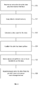
- Figure 1 shows an example approach for the pinned memory can be used in writing data.
- the block device interface receives an instruction to write data.
- the instruction to write data may be received as a function call of the interface.
- the data may be specified in the instruction with reference to a memory location.
- the instruction to write data may also comprise a destination at which the data should be written. This may be a reference to a location on one or more of the storage devices.
- the memory location of the data may correspond to a location in pinned memory. That is, the data is stored in a memory location which is accessible by the vector processor and by one or more other processors. In this manner, the driver may be running on the vector processor or another processor (such as a CPU).
- the memory location may be in main memory (that is, memory not accessible by a vector processor).
- the data is copied to pinned memory.
- one or more transforms may be performed to the data.
- one transform may involve encrypting or encoding the data. This may allow the data in pinned memory to be encrypted or encoded, even if the data in main memory is unencrypted or unencoded. Such transforms may be relatively fast so as to not materially delay a write process.
- Step 102 may only occur where the memory location in the instruction is not in pinned memory. That is, step 102 may be omitted where the data indicated in the request is already in pinned memory.
- a checksum for the data is calculated.
- the purpose of the checksum is to verify that the data which was written is the data that is subsequently retrieved. This can avoid the risk of bitrot, or otherwise of the data unexpectedly changing.
- the checksum may be a cryptographic hash, such that there is an extremely low probability that a change in the data would be unnoticeable.
- the checksum can then be stored in the cache, for example at the same location as the data.
- the checksum calculation may be relatively fast so as not to materially delay a write process.
- step 103 may be omitted.
- a checksum may be seen as unnecessary or the overhead associated with a checksum may be regarded as undesirable.
- the data is confirmed as having been written. This may involve returning a success value to the sender of the instruction, for example. In some cases, this may comprise confirming that the data has been written to the destination location specified in the instruction. In this way, the use of the cache is transparent to the user. From the user's point of view, the data has been stored at the specified storage device. This provides for compatibility and encapsulates the complexity which may otherwise be associated with using a cache.
- Step 104 may be particularly beneficial where the pinned memory corresponds to non-volatile memory. Because non-volatile memory is resistant against power loss, once the data has been written to the non-volatile memory, there may be a negligible chance of data loss. Thus by confirming that data has been written before the data has actually been written to the persistent storage device, this can provide a very fast data throughput without underlying risk of data loss.
- the vector processor performs one or more transforms on the data.
- These transforms can be invertible transforms, such that the original contents can be recovered by performing an inverse function.
- encryption, encoding, compression, deduplication, and the addition of further information are usually invertible functions, since the original information can be obtained by an inverse function.
- the transforms may be performed in a predetermined order. For example, encryption may be performed before encoding.
- One transform may be to encrypt the data. This can be performed using RSA, AES, or any other appropriate encryption algorithm. This may avoid the data being read if the underlying storage devices are compromised.
- Another transform may be to encode the data by adding parity information to the data through use of an error correcting code before splitting the data into data fragments. This allows for the original data to be recreated based on the fragments even if some fragments are erroneous.
- This error correcting code may be an erasure code, which allows for recreating the original data even if some of the fragments are entirely lost.
- a Reed-Solomon code is an example of an erasure code.
- a piece of data such as a block, is encoded using the Reed-Solomon algorithm to form a number of codewords.
- Each codeword comprises n symbols: k of these carry information from the original data, and the remaining are computed and can be used to reconstruct the original data.
- Each codeword can be broken up to form a data fragment.
- the parity n-k may be selected based on the type of data, system default, user preference or any other suitable approach. Because of how Reed-Solomon codes work, even if up to n-k fragments are lost, the original data can still be obtained.
- the vector processor may encode the data to form n data fragments, such that any k of the data fragments can be used to regenerate the data, k being less than or equal to n.
- this may include computing a cryptographic or non-cryptographic hash based on the data, and encoding this as part of the data.
- a further transform may be to log the storage event in an event log. This may include a timestamp and a cryptographic hash of the data. While logging does not affect the data being stored, it can be treated as a transform of the data for the purpose of the order of transforms.
- a vector processor By using a vector processor to perform the transforms, relatively high-quality transforms can be performed more efficiently compared to using a CPU. For example, in the case of encoding, a high level of parity may be used. In addition, this can be done in substantially real-time, so that the transforms do not materially delay the storage process (for example, by adding less than a few milliseconds of time to storage, for example).
- the pinned memory is configured to operate as a write-back cache.
- the driver In writing the data, the driver will determine a location in the cache at which the data should be written. If there is unused space in the cache, the data may be written there. If there is no unused space, the driver may move some of the existing data from the cache and to the one or more storage devices.
- the data is written to the cache at this location.
- Metadata at the driver may be updated to reflect this. For example, a mapping may be updated to show that the data intended to be stored at the destination location in the instruction is stored at the respective location in the cache. In addition, the location in the cache may be marked as dirty to indicate that the data stored there cannot be overwritten without being moved to one or more storage devices first.
- the driver asynchronously writes the data from the pinned memory to one or more storage devices.
- the driver may rely on one or more heuristics for this. For example, the driver may select the data to be m based on one or more of how old it is, how recent it was used, and how likely it is to be used.
- Step 106 may only be performed when the new data is needed to be written to the cache. In this way, the cache operates in a "lazy write" paradigm. Alternatively, in some cases the data may be immediately moved from the cache, for example where the data written is heuristically determined to be the best data to be moved.
- the driver writes the data to one or more of the storage devices.
- the one or more storage devices may be those specified in the initial instruction received at step 101 and recorded in metadata.
- step 106 is performed subsequently and asynchronously to step 103, the delays associated with typical storage devices are not apparent to a user in ordinary use. That is, the driver provides the appearance of data being stored at the much higher cache speed, rather than the lower storage device speed.
- non-volatile memory can mitigate or eliminate the "write hole" phenomenon. That is, in the case of volatile memory, if there is power loss during the transfer of data from the memory to a storage device, it can be impossible to determine if the data on disk was correctly transferred from memory. However, with non-volatile memory, the transfer process can resume without data loss when power is restored.
- the driver selectively moves data from the cache to the one or more storage devices when new data is needed to be written.
- the data is moved to one or more storage devices.
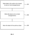
- Figure 2 shows an example approach for writing data from the write-back cache to one or more storage devices. This may be used to implement step 105.
- the driver selects the data at one or more blocks of the cache to be moved to one or more storage devices.
- the selection of the data in the cache to be moved may be made according to a heuristic using a number of variables. For example, this may be based on the age of the data, the most recent use of the data, the expected likelihood of use of the data, or the relationship between the data at the blocks.
- the driver writes the data to one or more storage devices. This may occur in a conventional manner by the driver interacting with a storage controller of the one or more storage devices.
- the selection of the one or more storage devices may be based on metadata previously stored for the data to be moved. That is, when the data was initially stored in the cache, metadata may have been updated to map between the cache location of the data and the eventual storage device location of the data. In such a case, this storage device location may be used to select the one or more storage devices.
- the driver marks the corresponding blocks of the cache as clean. This allows that part of the cache to be reused.
- the driver may also update the metadata to show that the data is no longer stored in the cache, for example by removing a mapping between a location in the cache and the data.
- the cache may be configured to retain a certain level of clean capacity. That is, data may be moved from the cache so that the cache can store a predetermined quantity of data without moving data. For example, it may be that 50% of the overall capacity of the cache should be retained as clean. This allows for improved burst performance in writing, while still allowing the improved read and modify performance for data already in the cache.
- the non-volatile write-back cache may be treated as a common resource available to all users. However, in some cases, a single user may monopolize the cache by writing a large amount of data at once. Once the cache is full, other users may not see the benefits
- the non-volatile write-back cache may be partitioned by source (such as user, or group of users). Each partition can then operate independently for caching and capacity purposes.
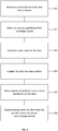
- Figure 3 shows an example of the use of a partitioned cache.
- the driver receives an instruction to write data. This may be the same as step 101. However, in this case, the instruction specifies a source of the instruction (such as a user or user group).
- the driver writes the data to a partition of the write-back cache, where the partition is associated with the source. This may be the same as step 102, except that the data is only written to that partition. If the partition has insufficient clean space, data will be moved out of that partition to the one or more storage devices (even if all other partitions in the cache are unused).
- the driver calculates a checksum for the data.
- the checksum can then be stored in the partition of the cache. This may be the same as step 103, except that the checksum may only be written to that partition.
- step 304 the driver confirms that the data has been written. This may be the same as step 104.
- the vector processor performs one or more invertible transforms on the data. This may be the same as step 105.
- the driver asynchronously writes the data from the pinned memory to one or more storage devices. This may be the same as step 106.
- the effect of a single source (such as a single user or user group) on the cache is substantially limited to their partition. This can preserve a high level of quality of service for multiple users, and avoids general performance degradation in response to bursts.
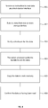
- Figure 4 shows an example approach for how the pinned memory can be used in reading data. This is an complement to the approach shown in Figure 1 .
- the block device interface receives an instruction to read data from one or more storage devices.
- the instruction to read data may be received as a function call of the interface.
- the instruction may specify the data with reference to a location on one or more storage devices or with reference to a meta-device.
- the data is retrieved from the one or more storage devices to the memory location.
- this may comprise retrieving the data from the underlying physical storage devices.
- the memory location of the data corresponds to a location in pinned memory. That is, the data is stored in a memory location which is accessible by the vector processor and by one or more other processors. In this manner, the driver may be running on the vector processor or another processor (such as a CPU).
- a checksum for the data is calculated. This can be compared to a previously calculated checksum for the data. This verifies that the data retrieved from the storage device is the same as the data that was stored at the storage device. In some cases, step 403 may be omitted. For example, in some implementations, verifying a checksum may be seen as unnecessary or the overhead associated with verifying a checksum may be regarded as undesirable.
- the vector processor performs one or more transforms on the data. These transforms may be the inverse of transforms performed at step 102 to recovers the original data. For example, decryption, decoding, decompression, un-deduplication, and the removal of further information may be performed to invert the transforms performed at step 102.
- the transforms may be performed in a predetermined order. For example, decoding may be performed before decryption.
- the data is copied to main memory.
- step 405 may be omitted.
- the data is confirmed as having been read. This may involve returning the memory location to the sender of the instruction, for example.
- FIG. 5 shows an example system which may be used to implement the methods noted above.
- the system 1000 comprises a CPU (central processing unit) 1010, a main memory 1020, one or more peripherals 1030, and a GPU (graphics processing unit) 1050.
- the CPU 1010, main memory 1020, peripherals 1030, and GPU 1050 are connected by a bus 1040.
- the bus 1040 includes a root complex, and each of the peripherals 1030 and the GPU 1050 are PCIe endpoints.
- the GPU 1050 can communicate with the peripherals 1030 directly via the bus 1040. In some cases, more than one CPU 1010 and/or more than one GPU 1050 is provided.
- the main memory 1020 comprises non-volatile memory chips configured to operate as a non-volatile write-back cache. This may involve the use of flash memory alone or in combination with conventional volatile memory.
- the non-volatile memory chips may be configured as non-volatile dual in-line memory module (NVDIMM).
- the main memory 1020 may further comprise conventional volatile memory, which is not used as the non-volatile write-back cache.
- the main memory 1020 comprises one or more pairs of non-volatile memory modules, such as a pair of NVDIMMs.
- data written to one of the non-volatile memory modules is mirrored on the other. This can provide a level of resilience in case of data loss: each non-volatile memory module contains the full set of data in the cache.
- the data may then be automatically mirrored to the new module.
- a first module of the pair can be replaced with a new larger one.
- the second module of the pair can then be replaced with a new larger one. This results in the cache being expanded (to the new larger size) without any loss of data or functionality.
- one or more of the non-volatile memory modules may be spanned, such that blocks are alternated between them. Spanning and mirroring may be combined. For example, of four non-volatile memory modules, a first and second module may be spanned, the first and second module may be mirrored to the third and fourth module.
- the peripherals 1030 may include persistent storage devices (such as hard disk drives, solid state drives, or the like), storage controllers (such as RAID controllers), network controllers (such as network interface cards), switches (such as PCIe switches configured to connect further peripherals), or any of a variety of devices.
- persistent storage devices such as hard disk drives, solid state drives, or the like
- storage controllers such as RAID controllers
- network controllers such as network interface cards
- switches such as PCIe switches configured to connect further peripherals
- main memory 1020 and any storage devices Atypical characteristic of the main memory 1020 and any storage devices is that main memory tends to be much faster for a random write. Thus writing a unit of data to main memory can typically be resolved much more quickly than writing a unit of data to a storage device.
- storage devices tend to be cheaper and larger, and are thus better for general long-term storage purposes.
- the peripherals 1030 and the GPU 1050 may have access to the main memory 1020 via the bus 1040.
- DMA direct memory access
- this can allow the peripheral 1030 or the GPU 1050 to read data to and write data from the main memory. This may involve copying the data from main memory 1020 to a memory local to the peripheral 1030 or the GPU 1050.
- the memory space for the CPU 1010 and the GPU 1050 can be shared via unified virtual memory. This allows for a pointer to a single memory address to be passed between the CPU and the GPU without the need to copy data between a main memory 1020 and a local memory.
- Computer system 500 may be used to implement the methods noted above.
- CPU 1010 or GPU 1050 may run a program which operates as a driver to one or more of the storage device peripherals 1030.
- a vector processor is a processor in which instructions are executed on an array of data. This can be contrasted to conventional CPUs which are scalar and execute an instruction on a single data item. This can allow a vector processor to process a large quantity of data much more quickly than a conventional, scalar CPU.
- a vector processor is a GPU.
- a vector processor may be implemented in other forms, such as a field programmable gate array (FPGA).
- FPGA field programmable gate array
- FIG. 6 An example GPU 950 which operates as a vector processor is shown in Figure 6 . Such a GPU 950 may be used as the vector processor in any of the approaches noted above.
- the GPU 950 comprises a number of SMs (streaming multiprocessors) 951, typically between 1 and 30. Each SM 951 has a shared memory 952 and an instruction unit 953.
- SMs streaming multiprocessors
- Each SM 951 comprises a number of SPs (streaming processors) 954, for example 8.
- SPs streaming processors
- Each SP 954 has access to the shared memory 952 and has a set of registers 955.
- Each SP 954 may also have access to a global memory 956 of the GPU. This global memory 956 may be mapped to main memory 920 of the computer system.
- the SPs 954 within an SM 951 receive instructions from the same instruction unit 953. In this way, each SP 954 within an SM typically processes the same instruction at the same time.
- the GPU 950 can be configured to run a kernel, which may be a program or function.
- the kernel may make use of the CUDA platform. Kernels are commonly relatively short-lived (that is, on the order of seconds), as a watchdog timer may kill a kernel if it runs beyond a preset threshold. However, in some cases a kernel may be long-running, in that it can execute indefinitely until execution finishes. Although a kernel runs on a GPU, it is typically initiated by a local or remote CPU.
- a kernel is executed by GPU 950 executing a grid corresponding to the kernel.
- a grid consists of a number of blocks. There is typically no synchronization between blocks in a grid.
- Each SM 951 can execute a block of the grid. Typically, an SM 951 can execute multiple blocks at the same time. The number of blocks on an SM 951 may be limited by the capacity of the shared memory 952. Typically, a block does not move from one SM 951 to another SM 951 during the execution of the kernel.
- Each SP 954 can execute a thread of the block. In some cases, one SP 954 can handle multiple threads at the same time.
- a thread is typically a computation comprising a number of instructions. Each instruction may take a number of cycles to perform, for example 4. Because of this latency, an SP 954 can execute multiple threads at once. That is, while one thread is being executed, another thread can be started. Threads may communicate with one another via shared memory 952 of the SM 951.
- the GPU 950 may have a SIMD (single instruction, multiple data) architecture. This means that a GPU 950 may operate on the basis of warps.
- Each warp comprises a number of threads within a block which execute the same instruction in lockstep, though optionally on different data. For example, each thread in a warp may execute an addition instruction to the numbers stored at different memory addresses. In addition, each thread within a warp may be configured to fetch data from memory at the same time.
- a warp is resident on an SM 951, such that each thread in a warp may be executed by a different SP 954 within an SM 951.
- the warp size (that is, the number of threads within a warp that can be executed in lockstep) may be a predetermined value, such as 32.
- An SM 951 may have multiple resident warps.
- a single kernel can utilize the capacity of the numerous processors available on a GPU. This can result in a kernel being executed significantly more quickly in comparison to other processing units.
- any of these methods may be embodied by a series of instructions, which may form a computer program. These instructions, or this computer program, may be stored on a computer readable medium, which may be non-transitory. When executed, these instructions or this program may cause a processor, such as a CPU or GPU, to perform the described methods.
- a processor such as a CPU or GPU
- processors may comprise a plurality of processors. That is, at least in the case of processors, the singular should be interpreted as including the plural.
- methods comprise multiple steps, different steps or different parts of a step may be performed by different processors.
- one step may be performed by a first type of processor (for example, processing of large sets of data may be performed by a GPU) and another step may be performed by a second type of processor (such as metadata lookup being performed by a CPU).
Landscapes
- Engineering & Computer Science (AREA)
- Theoretical Computer Science (AREA)
- Physics & Mathematics (AREA)
- General Engineering & Computer Science (AREA)
- General Physics & Mathematics (AREA)
- Software Systems (AREA)
- Human Computer Interaction (AREA)
- Computer Security & Cryptography (AREA)
- Quality & Reliability (AREA)
- Mathematical Physics (AREA)
- Computer Hardware Design (AREA)
- Information Retrieval, Db Structures And Fs Structures Therefor (AREA)
- Memory System Of A Hierarchy Structure (AREA)
- Complex Calculations (AREA)
- Signal Processing For Digital Recording And Reproducing (AREA)
- Detection And Correction Of Errors (AREA)
Applications Claiming Priority (3)
| Application Number | Priority Date | Filing Date | Title |
|---|---|---|---|
| US201862725703P | 2018-08-31 | 2018-08-31 | |
| US201862725691P | 2018-08-31 | 2018-08-31 | |
| US201862746981P | 2018-10-17 | 2018-10-17 |
Publications (2)
| Publication Number | Publication Date |
|---|---|
| EP3617892A1 true EP3617892A1 (de) | 2020-03-04 |
| EP3617892B1 EP3617892B1 (de) | 2022-05-11 |
Family
ID=67734509
Family Applications (4)
| Application Number | Title | Priority Date | Filing Date |
|---|---|---|---|
| EP24165253.6A Pending EP4404046A3 (de) | 2018-08-31 | 2019-08-22 | Verwaltung einer persistenten speichervorrichtung |
| EP19193027.0A Ceased EP3617868A1 (de) | 2018-08-31 | 2019-08-22 | Verwaltung einer persistenten speichervorrichtung |
| EP19194744.9A Active EP3617892B1 (de) | 2018-08-31 | 2019-08-30 | Blockvorrichtungsschnittstelle mit nichtflüchtigem nicht auslagerbarem speicher |
| EP19194748.0A Pending EP3627325A3 (de) | 2018-08-31 | 2019-08-30 | Vektorprozessorspeicherung |
Family Applications Before (2)
| Application Number | Title | Priority Date | Filing Date |
|---|---|---|---|
| EP24165253.6A Pending EP4404046A3 (de) | 2018-08-31 | 2019-08-22 | Verwaltung einer persistenten speichervorrichtung |
| EP19193027.0A Ceased EP3617868A1 (de) | 2018-08-31 | 2019-08-22 | Verwaltung einer persistenten speichervorrichtung |
Family Applications After (1)
| Application Number | Title | Priority Date | Filing Date |
|---|---|---|---|
| EP19194748.0A Pending EP3627325A3 (de) | 2018-08-31 | 2019-08-30 | Vektorprozessorspeicherung |
Country Status (5)
| Country | Link |
|---|---|
| US (10) | US11347653B2 (de) |
| EP (4) | EP4404046A3 (de) |
| JP (3) | JP2020042805A (de) |
| CN (3) | CN110874451A (de) |
| TW (3) | TW202011202A (de) |
Families Citing this family (8)
| Publication number | Priority date | Publication date | Assignee | Title |
|---|---|---|---|---|
| US11347653B2 (en) | 2018-08-31 | 2022-05-31 | Nyriad, Inc. | Persistent storage device management |
| CN111104047B (zh) * | 2018-10-25 | 2023-08-25 | 伊姆西Ip控股有限责任公司 | 管理冗余磁盘阵列的方法、设备和计算机可读存储介质 |
| US11907068B2 (en) * | 2021-02-16 | 2024-02-20 | Nyriad, Inc. | Read request response for reconstructed data in a degraded drive |
| EP4399612A4 (de) * | 2021-09-10 | 2025-07-23 | Purdue Research Foundation | Speicherverwaltungsverfahren für pseudofunktionelle differenzierbare programmierung |
| US12147680B2 (en) * | 2021-12-21 | 2024-11-19 | Daedalus Cloud Llc | Methods of administering metadata for persistent storage device |
| EP4202630A1 (de) | 2021-12-21 | 2023-06-28 | Nyriad, Inc. | Verfahren zur anordnung von daten auf einer persistenten speichervorrichtung |
| WO2024220365A1 (en) * | 2023-04-19 | 2024-10-24 | Daedalus Cloud Llc | Methods for continuously writing resilient data |
| WO2026049645A1 (ru) * | 2024-08-27 | 2026-03-05 | Акционерное Общество "Софит" | Векторное вычислительное устройство |
Citations (4)
| Publication number | Priority date | Publication date | Assignee | Title |
|---|---|---|---|---|
| US20090268903A1 (en) * | 2008-04-25 | 2009-10-29 | Netapp, Inc. | Network storage server with integrated encryption, compression and deduplication capability |
| US20130016109A1 (en) * | 2011-07-15 | 2013-01-17 | Kirill Garanzha | Out-of-core ray tracing with memory-efficient page generation |
| US20170132151A1 (en) * | 2015-11-09 | 2017-05-11 | International Business Machines Corporation | Implementing hardware accelerator for storage write cache management for destage operations from storage write cache |
| WO2019040418A1 (en) | 2017-08-22 | 2019-02-28 | Albert Einstein College Of Medicine, Inc. | VIRAL INHIBITOR WITH BROAD SPECTRUM |
Family Cites Families (80)
| Publication number | Priority date | Publication date | Assignee | Title |
|---|---|---|---|---|
| US5282274A (en) | 1990-05-24 | 1994-01-25 | International Business Machines Corporation | Translation of multiple virtual pages upon a TLB miss |
| US5502836A (en) * | 1991-11-21 | 1996-03-26 | Ast Research, Inc. | Method for disk restriping during system operation |
| US5459857A (en) * | 1992-05-15 | 1995-10-17 | Storage Technology Corporation | Fault tolerant disk array data storage subsystem |
| JPH0792790B2 (ja) * | 1992-11-18 | 1995-10-09 | 野木 達夫 | ベクトル並列計算機 |
| US6138126A (en) * | 1995-05-31 | 2000-10-24 | Network Appliance, Inc. | Method for allocating files in a file system integrated with a raid disk sub-system |
| JP3905992B2 (ja) * | 1999-03-23 | 2007-04-18 | 株式会社東芝 | デジタルデータ記録装置 |
| US6813688B2 (en) * | 2000-12-04 | 2004-11-02 | Sun Microsystems, Inc. | System and method for efficient data mirroring in a pair of storage devices |
| US20040123032A1 (en) | 2002-12-24 | 2004-06-24 | Talagala Nisha D. | Method for storing integrity metadata in redundant data layouts |
| US7111118B2 (en) | 2003-10-08 | 2006-09-19 | Lsi Logic Corporation | High performance raid mapping |
| US7418649B2 (en) * | 2005-03-15 | 2008-08-26 | Microsoft Corporation | Efficient implementation of reed-solomon erasure resilient codes in high-rate applications |
| JP2007140887A (ja) * | 2005-11-18 | 2007-06-07 | Hitachi Ltd | ストレージシステム、ディスクアレイ装置、ボリューム提示方法及びデータ一致性確認方法 |
| US7594087B2 (en) * | 2006-01-19 | 2009-09-22 | Sigmatel, Inc. | System and method for writing data to and erasing data from non-volatile memory |
| US7734890B2 (en) * | 2006-10-06 | 2010-06-08 | Okralabs Llc | Method and system for using a distributable virtual address space |
| US9632870B2 (en) | 2007-03-29 | 2017-04-25 | Violin Memory, Inc. | Memory system with multiple striping of raid groups and method for performing the same |
| US20090203430A1 (en) | 2008-02-07 | 2009-08-13 | Igt | Hybrid memory system and spin-buffer journaling in a gaming machine |
| KR101449524B1 (ko) | 2008-03-12 | 2014-10-14 | 삼성전자주식회사 | 스토리지 장치 및 컴퓨팅 시스템 |
| US20100037056A1 (en) * | 2008-08-07 | 2010-02-11 | Follis Benjamin D | Method to support privacy preserving secure data management in archival systems |
| US8874775B2 (en) * | 2008-10-15 | 2014-10-28 | Aster Risk Management Llc | Balancing a distributed system by replacing overloaded servers |
| CN101419573A (zh) * | 2008-12-01 | 2009-04-29 | 成都市华为赛门铁克科技有限公司 | 一种存储管理的方法、系统和存储设备 |
| KR101683286B1 (ko) | 2009-11-25 | 2016-12-06 | 삼성전자주식회사 | 이동통신망을 이용한 싱크 인증 시스템 및 방법 |
| WO2012052800A1 (en) | 2010-10-21 | 2012-04-26 | Oracle International Corp. | Two stage checksummed raid storage model |
| US9767098B2 (en) * | 2012-08-08 | 2017-09-19 | Amazon Technologies, Inc. | Archival data storage system |
| US9058223B2 (en) | 2011-04-22 | 2015-06-16 | Microsoft Technology Licensing Llc | Parallel entropy encoding on GPU |
| KR20120134919A (ko) * | 2011-06-03 | 2012-12-12 | 삼성전자주식회사 | 메모리 장치 |
| US9229809B2 (en) * | 2011-09-11 | 2016-01-05 | Microsoft Technology Licensing Llc | Nonvolatile media journaling of verified data sets |
| WO2013052562A1 (en) * | 2011-10-05 | 2013-04-11 | Lsi Corporation | Self-journaling and hierarchical consistency for non-volatile storage |
| CN103257831B (zh) * | 2012-02-20 | 2016-12-07 | 深圳市腾讯计算机系统有限公司 | 存储器的读写控制方法及对应的存储器 |
| WO2014003599A1 (en) | 2012-06-29 | 2014-01-03 | Ems Corparation | Redundant disc encoding via erasure decoding |
| FI125308B (en) * | 2012-07-05 | 2015-08-31 | Blancco Oy Ltd | Device, arrangement, method, and computer program for erasing data stored in mass storage |
| US9779035B1 (en) * | 2012-08-08 | 2017-10-03 | Amazon Technologies, Inc. | Log-based data storage on sequentially written media |
| US9164702B1 (en) * | 2012-09-07 | 2015-10-20 | Google Inc. | Single-sided distributed cache system |
| US9152552B2 (en) | 2012-09-11 | 2015-10-06 | International Business Machines Corporation | Securing sensitive information in a network cloud |
| US9639457B1 (en) | 2012-12-20 | 2017-05-02 | Datadirect Networks, Inc. | Data storage system and method for data migration between high-performance computing architectures and data storage devices using storage controller with distributed XOR capability |
| US9501276B2 (en) * | 2012-12-31 | 2016-11-22 | Intel Corporation | Instructions and logic to vectorize conditional loops |
| US9395924B2 (en) * | 2013-01-22 | 2016-07-19 | Seagate Technology Llc | Management of and region selection for writes to non-volatile memory |
| US9092152B1 (en) | 2013-03-14 | 2015-07-28 | Datadirect Networks, Inc. | Data storage system employing a distributed compute engine memory controller with embedded logic and arithmetic functionality and method for data migration between high-performance computing architectures and data storage devices using the same |
| US9792220B2 (en) | 2013-03-15 | 2017-10-17 | Nvidia Corporation | Microcontroller for memory management unit |
| US9213633B2 (en) * | 2013-04-30 | 2015-12-15 | Seagate Technology Llc | Flash translation layer with lower write amplification |
| US9158927B1 (en) | 2013-06-24 | 2015-10-13 | Amazon Technologies, Inc. | Cross-region recovery of encrypted, erasure-encoded data |
| US9311011B2 (en) * | 2013-08-07 | 2016-04-12 | Qualcomm Incorporated | Dynamic address negotiation for shared memory regions in heterogenous multiprocessor systems |
| US9405623B2 (en) * | 2013-09-25 | 2016-08-02 | Xyratex Technology Limited | Method of, and apparatus for, layout rectification of erasure encoded storage systems |
| US9571125B2 (en) * | 2013-10-03 | 2017-02-14 | Futurewei Technologies, Inc. | Systems and methods of vector-DMA cache-XOR for MPCC erasure coding |
| US9223843B1 (en) * | 2013-12-02 | 2015-12-29 | Amazon Technologies, Inc. | Optimized log storage for asynchronous log updates |
| US9268640B1 (en) | 2013-12-20 | 2016-02-23 | Emc Corporation | Limiting data loss on parity RAID groups |
| US9483349B2 (en) | 2014-01-17 | 2016-11-01 | Netapp, Inc. | Clustered raid data organization |
| US9075773B1 (en) * | 2014-05-07 | 2015-07-07 | Igneous Systems, Inc. | Prioritized repair of data storage failures |
| CN104063186B (zh) * | 2014-06-30 | 2016-04-06 | 成都万维图新信息技术有限公司 | 一种电子设备的数据访问方法 |
| CN104410725A (zh) | 2014-09-17 | 2015-03-11 | 广州杰赛科技股份有限公司 | Gpu的处理方法、系统以及基于gpu的dns解析方法和系统 |
| RU2580016C1 (ru) | 2014-10-17 | 2016-04-10 | Закрытое акционерное общество "Лаборатория Касперского" | Способ передачи управления между областями памяти |
| US9921910B2 (en) * | 2015-02-19 | 2018-03-20 | Netapp, Inc. | Virtual chunk service based data recovery in a distributed data storage system |
| US9811275B2 (en) * | 2015-02-27 | 2017-11-07 | Toshiba Memory Corporation | Memory system and data control method |
| JP6385570B2 (ja) * | 2015-05-12 | 2018-09-05 | 株式会社日立製作所 | ストレージシステムおよび記憶制御方法 |
| US9823843B2 (en) * | 2015-07-23 | 2017-11-21 | Qualcomm Incorporated | Memory hierarchy monitoring systems and methods |
| CN105141891B (zh) * | 2015-08-04 | 2019-04-30 | 浙江宇视科技有限公司 | 一种警前录像缓存方法和装置 |
| US9823968B1 (en) | 2015-08-21 | 2017-11-21 | Datadirect Networks, Inc. | Data storage system employing a variable redundancy distributed RAID controller with embedded RAID logic and method for data migration between high-performance computing architectures and data storage devices using the same |
| US10445850B2 (en) | 2015-08-26 | 2019-10-15 | Intel Corporation | Technologies for offloading network packet processing to a GPU |
| JP6113816B1 (ja) * | 2015-11-18 | 2017-04-12 | 株式会社東芝 | 情報処理システム、情報処理装置、及びプログラム |
| US10216419B2 (en) | 2015-11-19 | 2019-02-26 | HGST Netherlands B.V. | Direct interface between graphics processing unit and data storage unit |
| US20170206033A1 (en) | 2016-01-19 | 2017-07-20 | SK Hynix Inc. | Mechanism enabling the use of slow memory to achieve byte addressability and near-dram performance with page remapping scheme |
| EP3203377A1 (de) * | 2016-02-08 | 2017-08-09 | Wipro Limited | Verfahren und system zur optimierten speicherbereinigung in einer speichervorrichtung |
| CN107102957A (zh) | 2016-02-22 | 2017-08-29 | 深圳市知穹科技有限公司 | 一种基于gpu与nic之间的内存高速直接交换的方法及系统 |
| ES2899933T3 (es) | 2016-03-15 | 2022-03-15 | Datomia Res Labs Ou | Gestión y seguridad de datos del sistema de almacenamiento distribuido |
| US10248326B2 (en) * | 2016-06-29 | 2019-04-02 | EMC IP Holding Company LLC | Incremental erasure coding for storage systems |
| US10152376B2 (en) * | 2016-06-29 | 2018-12-11 | EMC IP Holding Company LLC | Data object recovery for storage systems |
| TWI592799B (zh) * | 2016-07-01 | 2017-07-21 | 群聯電子股份有限公司 | 映射表更新方法、記憶體控制電路單元及記憶體儲存裝置 |
| US10739996B1 (en) * | 2016-07-18 | 2020-08-11 | Seagate Technology Llc | Enhanced garbage collection |
| CN106383666B (zh) * | 2016-09-07 | 2020-05-01 | 东信和平科技股份有限公司 | 一种数据存储方法及装置 |
| US9996411B1 (en) | 2016-11-29 | 2018-06-12 | International Business Machines Corporation | In-channel memory mirroring |
| US10296224B2 (en) | 2016-12-21 | 2019-05-21 | Intel Corporation | Apparatus, system and method for increasing the capacity of a storage device available to store user data |
| US20180181324A1 (en) | 2016-12-26 | 2018-06-28 | EMC IP Holding Company LLC | Data protection with erasure coding and xor |
| WO2019050418A1 (en) | 2017-09-11 | 2019-03-14 | Nyriad Limited | COMPRESSION OF DATA BASED ON A DICTIONARY |
| CN109542335B (zh) * | 2017-09-22 | 2022-04-01 | 慧荣科技股份有限公司 | 快闪存储器的数据内部搬移方法以及使用该方法的装置 |
| US10394706B2 (en) * | 2017-11-02 | 2019-08-27 | Western Digital Technologies, Inc. | Non-volatile storage with adaptive command prediction |
| CN107844431B (zh) * | 2017-11-03 | 2022-01-25 | 合肥兆芯电子有限公司 | 映射表更新方法、存储器控制电路单元与存储器存储装置 |
| WO2019118356A1 (en) | 2017-12-11 | 2019-06-20 | Fungible, Inc. | Durable block storage in data center access nodes with inline erasure coding |
| US10509698B2 (en) | 2018-02-27 | 2019-12-17 | Goke Us Research Laboratory | Method and apparatus for data encoding and decoding using a standardized data storage and retrieval protocol |
| CN115509961B (zh) * | 2018-06-25 | 2026-03-17 | 慧荣科技股份有限公司 | 实体存储对照表产生装置及方法 |
| US10783022B2 (en) * | 2018-08-03 | 2020-09-22 | EMC IP Holding Company LLC | Immediate replication for dedicated data blocks |
| US11347653B2 (en) | 2018-08-31 | 2022-05-31 | Nyriad, Inc. | Persistent storage device management |
| US11115057B2 (en) * | 2020-02-07 | 2021-09-07 | EMC IP Holding Company LLC | Efficient erasure coding of mid-size data objects |
-
2019
- 2019-08-19 US US16/544,605 patent/US11347653B2/en active Active
- 2019-08-21 TW TW108129760A patent/TW202011202A/zh unknown
- 2019-08-22 EP EP24165253.6A patent/EP4404046A3/de active Pending
- 2019-08-22 EP EP19193027.0A patent/EP3617868A1/de not_active Ceased
- 2019-08-28 JP JP2019156155A patent/JP2020042805A/ja active Pending
- 2019-08-29 JP JP2019156878A patent/JP2020038649A/ja active Pending
- 2019-08-29 JP JP2019157181A patent/JP2020038650A/ja active Pending
- 2019-08-30 US US16/556,711 patent/US11263145B2/en active Active
- 2019-08-30 EP EP19194744.9A patent/EP3617892B1/de active Active
- 2019-08-30 CN CN201910816269.XA patent/CN110874451A/zh active Pending
- 2019-08-30 TW TW108131172A patent/TW202014884A/zh unknown
- 2019-08-30 EP EP19194748.0A patent/EP3627325A3/de active Pending
- 2019-08-30 US US16/556,575 patent/US11263144B2/en active Active
- 2019-08-30 TW TW108131168A patent/TW202014908A/zh unknown
- 2019-08-30 CN CN201910817188.1A patent/CN110874194A/zh active Pending
- 2019-08-30 CN CN201910815672.0A patent/CN110874193A/zh active Pending
-
2022
- 2022-01-19 US US17/579,264 patent/US12086070B2/en active Active
- 2022-02-01 US US17/590,721 patent/US11782844B2/en active Active
- 2022-04-27 US US17/731,038 patent/US12229055B2/en active Active
-
2023
- 2023-09-07 US US18/463,256 patent/US12235772B2/en active Active
-
2024
- 2024-07-18 US US18/777,334 patent/US20240370377A1/en active Pending
-
2025
- 2025-01-03 US US19/009,685 patent/US20250139014A1/en active Pending
- 2025-01-14 US US19/020,108 patent/US20250156335A1/en active Pending
Patent Citations (4)
| Publication number | Priority date | Publication date | Assignee | Title |
|---|---|---|---|---|
| US20090268903A1 (en) * | 2008-04-25 | 2009-10-29 | Netapp, Inc. | Network storage server with integrated encryption, compression and deduplication capability |
| US20130016109A1 (en) * | 2011-07-15 | 2013-01-17 | Kirill Garanzha | Out-of-core ray tracing with memory-efficient page generation |
| US20170132151A1 (en) * | 2015-11-09 | 2017-05-11 | International Business Machines Corporation | Implementing hardware accelerator for storage write cache management for destage operations from storage write cache |
| WO2019040418A1 (en) | 2017-08-22 | 2019-02-28 | Albert Einstein College Of Medicine, Inc. | VIRAL INHIBITOR WITH BROAD SPECTRUM |
Non-Patent Citations (2)
| Title |
|---|
| ANONYMOUS: "CUDA 2.2 Pinned Memory APIs", 1 March 2009 (2009-03-01), XP055655605, Retrieved from the Internet <URL:https://devtalk.nvidia.com/cmd/default/download-comment-attachment/50683/> [retrieved on 20200108] * |
| ANUJAN VARMA ET AL: "Destage algorithms for disk arrays with non-volatile caches", ACM SIGARCH COMPUTER ARCHITECTURE NEWS, ACM SPECIAL INTEREST GROUP ON COMPUTER ARCHITECTURE, 2 PENN PLAZA, SUITE 701 NEW YORK NY 10121-0701 USA, vol. 23, no. 2, 1 May 1995 (1995-05-01), pages 83 - 95, XP058084661, ISSN: 0163-5964, DOI: 10.1145/225830.224042 * |
Also Published As
| Publication number | Publication date |
|---|---|
| US12235772B2 (en) | 2025-02-25 |
| CN110874194A (zh) | 2020-03-10 |
| US20250139014A1 (en) | 2025-05-01 |
| US20250156335A1 (en) | 2025-05-15 |
| EP4404046A2 (de) | 2024-07-24 |
| US11263145B2 (en) | 2022-03-01 |
| CN110874193A (zh) | 2020-03-10 |
| CN110874451A (zh) | 2020-03-10 |
| US20220156200A1 (en) | 2022-05-19 |
| US20220253385A1 (en) | 2022-08-11 |
| US12086070B2 (en) | 2024-09-10 |
| TW202011202A (zh) | 2020-03-16 |
| US20240370377A1 (en) | 2024-11-07 |
| US20220138111A1 (en) | 2022-05-05 |
| US11263144B2 (en) | 2022-03-01 |
| US20200073663A1 (en) | 2020-03-05 |
| EP3627325A3 (de) | 2020-07-29 |
| TW202014908A (zh) | 2020-04-16 |
| JP2020038650A (ja) | 2020-03-12 |
| JP2020042805A (ja) | 2020-03-19 |
| JP2020038649A (ja) | 2020-03-12 |
| EP3617868A1 (de) | 2020-03-04 |
| US12229055B2 (en) | 2025-02-18 |
| US11782844B2 (en) | 2023-10-10 |
| EP3627325A2 (de) | 2020-03-25 |
| US20200073818A1 (en) | 2020-03-05 |
| TW202014884A (zh) | 2020-04-16 |
| US11347653B2 (en) | 2022-05-31 |
| EP3617892B1 (de) | 2022-05-11 |
| US20200073824A1 (en) | 2020-03-05 |
| US20230418761A1 (en) | 2023-12-28 |
| EP4404046A3 (de) | 2024-10-30 |
Similar Documents
| Publication | Publication Date | Title |
|---|---|---|
| US12086070B2 (en) | Block device interface using non-volatile pinned memory | |
| US11340985B2 (en) | Reliability coding for storage on a network | |
| US8583984B2 (en) | Method and apparatus for increasing data reliability for raid operations | |
| US9823968B1 (en) | Data storage system employing a variable redundancy distributed RAID controller with embedded RAID logic and method for data migration between high-performance computing architectures and data storage devices using the same | |
| US8037391B1 (en) | Raid-6 computation system and method | |
| JP2020095722A (ja) | 誤り訂正符号加速装置及びシステム | |
| WO2012050935A2 (en) | Apparatus, system, and method for data transformations within a data storage device | |
| EP4145265A2 (de) | Speichersystem | |
| US20250355589A1 (en) | Systems, methods, and apparatus for hierarchical aggregation for computational storage | |
| US10095542B2 (en) | Cooperative thread array granularity context switch during trap handling | |
| KR101970864B1 (ko) | 총 플래시 어레이 기반 오픈스택 클라우드 블록 스토리지에서의 패리티 데이터 중복제거 방법 | |
| US12346203B2 (en) | Read request response for reconstructed data in a degraded drive | |
| HK40025857A (en) | Block device interface using non-volatile pinned memory | |
| WO2020086850A2 (en) | Flexible reliability coding for storage on a network | |
| US9645745B2 (en) | I/O performance in resilient arrays of computer storage devices | |
| HK40025858A (en) | Vector processor storage | |
| US9830094B2 (en) | Dynamic transitioning of protection information in array systems | |
| HK40025859A (en) | Persistent storage device management |
Legal Events
| Date | Code | Title | Description |
|---|---|---|---|
| PUAI | Public reference made under article 153(3) epc to a published international application that has entered the european phase |
Free format text: ORIGINAL CODE: 0009012 |
|
| STAA | Information on the status of an ep patent application or granted ep patent |
Free format text: STATUS: THE APPLICATION HAS BEEN PUBLISHED |
|
| AK | Designated contracting states |
Kind code of ref document: A1 Designated state(s): AL AT BE BG CH CY CZ DE DK EE ES FI FR GB GR HR HU IE IS IT LI LT LU LV MC MK MT NL NO PL PT RO RS SE SI SK SM TR |
|
| AX | Request for extension of the european patent |
Extension state: BA ME |
|
| STAA | Information on the status of an ep patent application or granted ep patent |
Free format text: STATUS: REQUEST FOR EXAMINATION WAS MADE |
|
| 17P | Request for examination filed |
Effective date: 20200826 |
|
| RBV | Designated contracting states (corrected) |
Designated state(s): AL AT BE BG CH CY CZ DE DK EE ES FI FR GB GR HR HU IE IS IT LI LT LU LV MC MK MT NL NO PL PT RO RS SE SI SK SM TR |
|
| REG | Reference to a national code |
Ref country code: DE Ref legal event code: R079 Ref document number: 602019014784 Country of ref document: DE Free format text: PREVIOUS MAIN CLASS: G06F0012080400 Ipc: G06F0012086800 |
|
| GRAP | Despatch of communication of intention to grant a patent |
Free format text: ORIGINAL CODE: EPIDOSNIGR1 |
|
| STAA | Information on the status of an ep patent application or granted ep patent |
Free format text: STATUS: GRANT OF PATENT IS INTENDED |
|
| RIC1 | Information provided on ipc code assigned before grant |
Ipc: G06F 13/16 20060101ALN20211018BHEP Ipc: G06F 12/126 20160101ALN20211018BHEP Ipc: G06F 11/10 20060101ALI20211018BHEP Ipc: G06F 3/06 20060101ALI20211018BHEP Ipc: G06F 9/38 20180101ALI20211018BHEP Ipc: G06F 15/167 20060101ALI20211018BHEP Ipc: G06F 12/0842 20160101ALI20211018BHEP Ipc: G06F 12/0871 20160101ALI20211018BHEP Ipc: G06F 12/0868 20160101AFI20211018BHEP |
|
| INTG | Intention to grant announced |
Effective date: 20211112 |
|
| GRAS | Grant fee paid |
Free format text: ORIGINAL CODE: EPIDOSNIGR3 |
|
| RAP3 | Party data changed (applicant data changed or rights of an application transferred) |
Owner name: NYRIAD |
|
| GRAA | (expected) grant |
Free format text: ORIGINAL CODE: 0009210 |
|
| STAA | Information on the status of an ep patent application or granted ep patent |
Free format text: STATUS: THE PATENT HAS BEEN GRANTED |
|
| RAP1 | Party data changed (applicant data changed or rights of an application transferred) |
Owner name: NYRIAD, INC. |
|
| AK | Designated contracting states |
Kind code of ref document: B1 Designated state(s): AL AT BE BG CH CY CZ DE DK EE ES FI FR GB GR HR HU IE IS IT LI LT LU LV MC MK MT NL NO PL PT RO RS SE SI SK SM TR |
|
| REG | Reference to a national code |
Ref country code: GB Ref legal event code: FG4D |
|
| REG | Reference to a national code |
Ref country code: CH Ref legal event code: EP |
|
| REG | Reference to a national code |
Ref country code: AT Ref legal event code: REF Ref document number: 1492042 Country of ref document: AT Kind code of ref document: T Effective date: 20220515 |
|
| REG | Reference to a national code |
Ref country code: DE Ref legal event code: R096 Ref document number: 602019014784 Country of ref document: DE |
|
| REG | Reference to a national code |
Ref country code: IE Ref legal event code: FG4D |
|
| REG | Reference to a national code |
Ref country code: NL Ref legal event code: FP |
|
| REG | Reference to a national code |
Ref country code: LT Ref legal event code: MG9D |
|
| REG | Reference to a national code |
Ref country code: AT Ref legal event code: MK05 Ref document number: 1492042 Country of ref document: AT Kind code of ref document: T Effective date: 20220511 |
|
| PG25 | Lapsed in a contracting state [announced via postgrant information from national office to epo] |
Ref country code: SE Free format text: LAPSE BECAUSE OF FAILURE TO SUBMIT A TRANSLATION OF THE DESCRIPTION OR TO PAY THE FEE WITHIN THE PRESCRIBED TIME-LIMIT Effective date: 20220511 Ref country code: PT Free format text: LAPSE BECAUSE OF FAILURE TO SUBMIT A TRANSLATION OF THE DESCRIPTION OR TO PAY THE FEE WITHIN THE PRESCRIBED TIME-LIMIT Effective date: 20220912 Ref country code: NO Free format text: LAPSE BECAUSE OF FAILURE TO SUBMIT A TRANSLATION OF THE DESCRIPTION OR TO PAY THE FEE WITHIN THE PRESCRIBED TIME-LIMIT Effective date: 20220811 Ref country code: LT Free format text: LAPSE BECAUSE OF FAILURE TO SUBMIT A TRANSLATION OF THE DESCRIPTION OR TO PAY THE FEE WITHIN THE PRESCRIBED TIME-LIMIT Effective date: 20220511 Ref country code: HR Free format text: LAPSE BECAUSE OF FAILURE TO SUBMIT A TRANSLATION OF THE DESCRIPTION OR TO PAY THE FEE WITHIN THE PRESCRIBED TIME-LIMIT Effective date: 20220511 Ref country code: GR Free format text: LAPSE BECAUSE OF FAILURE TO SUBMIT A TRANSLATION OF THE DESCRIPTION OR TO PAY THE FEE WITHIN THE PRESCRIBED TIME-LIMIT Effective date: 20220812 Ref country code: FI Free format text: LAPSE BECAUSE OF FAILURE TO SUBMIT A TRANSLATION OF THE DESCRIPTION OR TO PAY THE FEE WITHIN THE PRESCRIBED TIME-LIMIT Effective date: 20220511 Ref country code: ES Free format text: LAPSE BECAUSE OF FAILURE TO SUBMIT A TRANSLATION OF THE DESCRIPTION OR TO PAY THE FEE WITHIN THE PRESCRIBED TIME-LIMIT Effective date: 20220511 Ref country code: BG Free format text: LAPSE BECAUSE OF FAILURE TO SUBMIT A TRANSLATION OF THE DESCRIPTION OR TO PAY THE FEE WITHIN THE PRESCRIBED TIME-LIMIT Effective date: 20220811 Ref country code: AT Free format text: LAPSE BECAUSE OF FAILURE TO SUBMIT A TRANSLATION OF THE DESCRIPTION OR TO PAY THE FEE WITHIN THE PRESCRIBED TIME-LIMIT Effective date: 20220511 |
|
| PG25 | Lapsed in a contracting state [announced via postgrant information from national office to epo] |
Ref country code: RS Free format text: LAPSE BECAUSE OF FAILURE TO SUBMIT A TRANSLATION OF THE DESCRIPTION OR TO PAY THE FEE WITHIN THE PRESCRIBED TIME-LIMIT Effective date: 20220511 Ref country code: PL Free format text: LAPSE BECAUSE OF FAILURE TO SUBMIT A TRANSLATION OF THE DESCRIPTION OR TO PAY THE FEE WITHIN THE PRESCRIBED TIME-LIMIT Effective date: 20220511 Ref country code: LV Free format text: LAPSE BECAUSE OF FAILURE TO SUBMIT A TRANSLATION OF THE DESCRIPTION OR TO PAY THE FEE WITHIN THE PRESCRIBED TIME-LIMIT Effective date: 20220511 Ref country code: IS Free format text: LAPSE BECAUSE OF FAILURE TO SUBMIT A TRANSLATION OF THE DESCRIPTION OR TO PAY THE FEE WITHIN THE PRESCRIBED TIME-LIMIT Effective date: 20220911 |
|
| PG25 | Lapsed in a contracting state [announced via postgrant information from national office to epo] |
Ref country code: SM Free format text: LAPSE BECAUSE OF FAILURE TO SUBMIT A TRANSLATION OF THE DESCRIPTION OR TO PAY THE FEE WITHIN THE PRESCRIBED TIME-LIMIT Effective date: 20220511 Ref country code: SK Free format text: LAPSE BECAUSE OF FAILURE TO SUBMIT A TRANSLATION OF THE DESCRIPTION OR TO PAY THE FEE WITHIN THE PRESCRIBED TIME-LIMIT Effective date: 20220511 Ref country code: RO Free format text: LAPSE BECAUSE OF FAILURE TO SUBMIT A TRANSLATION OF THE DESCRIPTION OR TO PAY THE FEE WITHIN THE PRESCRIBED TIME-LIMIT Effective date: 20220511 Ref country code: EE Free format text: LAPSE BECAUSE OF FAILURE TO SUBMIT A TRANSLATION OF THE DESCRIPTION OR TO PAY THE FEE WITHIN THE PRESCRIBED TIME-LIMIT Effective date: 20220511 Ref country code: DK Free format text: LAPSE BECAUSE OF FAILURE TO SUBMIT A TRANSLATION OF THE DESCRIPTION OR TO PAY THE FEE WITHIN THE PRESCRIBED TIME-LIMIT Effective date: 20220511 Ref country code: CZ Free format text: LAPSE BECAUSE OF FAILURE TO SUBMIT A TRANSLATION OF THE DESCRIPTION OR TO PAY THE FEE WITHIN THE PRESCRIBED TIME-LIMIT Effective date: 20220511 |
|
| REG | Reference to a national code |
Ref country code: DE Ref legal event code: R097 Ref document number: 602019014784 Country of ref document: DE |
|
| PLBE | No opposition filed within time limit |
Free format text: ORIGINAL CODE: 0009261 |
|
| STAA | Information on the status of an ep patent application or granted ep patent |
Free format text: STATUS: NO OPPOSITION FILED WITHIN TIME LIMIT |
|
| PG25 | Lapsed in a contracting state [announced via postgrant information from national office to epo] |
Ref country code: MC Free format text: LAPSE BECAUSE OF FAILURE TO SUBMIT A TRANSLATION OF THE DESCRIPTION OR TO PAY THE FEE WITHIN THE PRESCRIBED TIME-LIMIT Effective date: 20220511 Ref country code: AL Free format text: LAPSE BECAUSE OF FAILURE TO SUBMIT A TRANSLATION OF THE DESCRIPTION OR TO PAY THE FEE WITHIN THE PRESCRIBED TIME-LIMIT Effective date: 20220511 |
|
| REG | Reference to a national code |
Ref country code: CH Ref legal event code: PL |
|
| 26N | No opposition filed |
Effective date: 20230214 |
|
| PG25 | Lapsed in a contracting state [announced via postgrant information from national office to epo] |
Ref country code: LU Free format text: LAPSE BECAUSE OF NON-PAYMENT OF DUE FEES Effective date: 20220830 Ref country code: LI Free format text: LAPSE BECAUSE OF NON-PAYMENT OF DUE FEES Effective date: 20220831 Ref country code: CH Free format text: LAPSE BECAUSE OF NON-PAYMENT OF DUE FEES Effective date: 20220831 |
|
| REG | Reference to a national code |
Ref country code: BE Ref legal event code: MM Effective date: 20220831 |
|
| PG25 | Lapsed in a contracting state [announced via postgrant information from national office to epo] |
Ref country code: SI Free format text: LAPSE BECAUSE OF FAILURE TO SUBMIT A TRANSLATION OF THE DESCRIPTION OR TO PAY THE FEE WITHIN THE PRESCRIBED TIME-LIMIT Effective date: 20220511 |
|
| PG25 | Lapsed in a contracting state [announced via postgrant information from national office to epo] |
Ref country code: BE Free format text: LAPSE BECAUSE OF NON-PAYMENT OF DUE FEES Effective date: 20220831 |
|
| PG25 | Lapsed in a contracting state [announced via postgrant information from national office to epo] |
Ref country code: IT Free format text: LAPSE BECAUSE OF FAILURE TO SUBMIT A TRANSLATION OF THE DESCRIPTION OR TO PAY THE FEE WITHIN THE PRESCRIBED TIME-LIMIT Effective date: 20220511 |
|
| PG25 | Lapsed in a contracting state [announced via postgrant information from national office to epo] |
Ref country code: HU Free format text: LAPSE BECAUSE OF FAILURE TO SUBMIT A TRANSLATION OF THE DESCRIPTION OR TO PAY THE FEE WITHIN THE PRESCRIBED TIME-LIMIT; INVALID AB INITIO Effective date: 20190830 |
|
| PG25 | Lapsed in a contracting state [announced via postgrant information from national office to epo] |
Ref country code: CY Free format text: LAPSE BECAUSE OF FAILURE TO SUBMIT A TRANSLATION OF THE DESCRIPTION OR TO PAY THE FEE WITHIN THE PRESCRIBED TIME-LIMIT Effective date: 20220511 |
|
| REG | Reference to a national code |
Ref country code: DE Ref legal event code: R081 Ref document number: 602019014784 Country of ref document: DE Owner name: DAEDALUS CLOUD LLC, CROTON-ON-HUDSON, US Free format text: FORMER OWNER: NYRIAD, INC., DOVER, DE, US |
|
| PG25 | Lapsed in a contracting state [announced via postgrant information from national office to epo] |
Ref country code: MK Free format text: LAPSE BECAUSE OF FAILURE TO SUBMIT A TRANSLATION OF THE DESCRIPTION OR TO PAY THE FEE WITHIN THE PRESCRIBED TIME-LIMIT Effective date: 20220511 |
|
| REG | Reference to a national code |
Ref country code: GB Ref legal event code: 732E Free format text: REGISTERED BETWEEN 20240530 AND 20240605 |
|
| PG25 | Lapsed in a contracting state [announced via postgrant information from national office to epo] |
Ref country code: TR Free format text: LAPSE BECAUSE OF FAILURE TO SUBMIT A TRANSLATION OF THE DESCRIPTION OR TO PAY THE FEE WITHIN THE PRESCRIBED TIME-LIMIT Effective date: 20220511 |
|
| REG | Reference to a national code |
Ref country code: NL Ref legal event code: PD Owner name: DAEDALUS CLOUD LLC; US Free format text: DETAILS ASSIGNMENT: CHANGE OF OWNER(S), ASSIGNMENT; FORMER OWNER NAME: NYRIAD, INC. Effective date: 20240805 |
|
| PG25 | Lapsed in a contracting state [announced via postgrant information from national office to epo] |
Ref country code: MT Free format text: LAPSE BECAUSE OF FAILURE TO SUBMIT A TRANSLATION OF THE DESCRIPTION OR TO PAY THE FEE WITHIN THE PRESCRIBED TIME-LIMIT Effective date: 20220511 |
|
| PG25 | Lapsed in a contracting state [announced via postgrant information from national office to epo] |
Ref country code: BG Free format text: LAPSE BECAUSE OF FAILURE TO SUBMIT A TRANSLATION OF THE DESCRIPTION OR TO PAY THE FEE WITHIN THE PRESCRIBED TIME-LIMIT Effective date: 20220511 |
|
| PG25 | Lapsed in a contracting state [announced via postgrant information from national office to epo] |
Ref country code: BG Free format text: LAPSE BECAUSE OF FAILURE TO SUBMIT A TRANSLATION OF THE DESCRIPTION OR TO PAY THE FEE WITHIN THE PRESCRIBED TIME-LIMIT Effective date: 20220511 |
|
| PGFP | Annual fee paid to national office [announced via postgrant information from national office to epo] |
Ref country code: NL Payment date: 20250825 Year of fee payment: 7 |
|
| PGFP | Annual fee paid to national office [announced via postgrant information from national office to epo] |
Ref country code: DE Payment date: 20250827 Year of fee payment: 7 |
|
| PGFP | Annual fee paid to national office [announced via postgrant information from national office to epo] |
Ref country code: GB Payment date: 20250826 Year of fee payment: 7 |
|
| PGFP | Annual fee paid to national office [announced via postgrant information from national office to epo] |
Ref country code: FR Payment date: 20250825 Year of fee payment: 7 |
|
| PGFP | Annual fee paid to national office [announced via postgrant information from national office to epo] |
Ref country code: IE Payment date: 20250819 Year of fee payment: 7 |