EP3618103A1 - Strukturierungsmethode - Google Patents
Strukturierungsmethode Download PDFInfo
- Publication number
- EP3618103A1 EP3618103A1 EP18191776.6A EP18191776A EP3618103A1 EP 3618103 A1 EP3618103 A1 EP 3618103A1 EP 18191776 A EP18191776 A EP 18191776A EP 3618103 A1 EP3618103 A1 EP 3618103A1
- Authority
- EP
- European Patent Office
- Prior art keywords
- layer
- trenches
- mask
- patterning
- memorization
- Prior art date
- Legal status (The legal status is an assumption and is not a legal conclusion. Google has not performed a legal analysis and makes no representation as to the accuracy of the status listed.)
- Withdrawn
Links
Images







Classifications
-
- G—PHYSICS
- G03—PHOTOGRAPHY; CINEMATOGRAPHY; ANALOGOUS TECHNIQUES USING WAVES OTHER THAN OPTICAL WAVES; ELECTROGRAPHY; HOLOGRAPHY
- G03F—PHOTOMECHANICAL PRODUCTION OF TEXTURED OR PATTERNED SURFACES, e.g. FOR PRINTING, FOR PROCESSING OF SEMICONDUCTOR DEVICES; MATERIALS THEREFOR; ORIGINALS THEREFOR; APPARATUS SPECIALLY ADAPTED THEREFOR
- G03F7/00—Photomechanical, e.g. photolithographic, production of textured or patterned surfaces, e.g. printing surfaces; Materials therefor, e.g. comprising photoresists; Apparatus specially adapted therefor
- G03F7/16—Coating processes; Apparatus therefor
-
- H—ELECTRICITY
- H10—SEMICONDUCTOR DEVICES; ELECTRIC SOLID-STATE DEVICES NOT OTHERWISE PROVIDED FOR
- H10W—GENERIC PACKAGES, INTERCONNECTIONS, CONNECTORS OR OTHER CONSTRUCTIONAL DETAILS OF DEVICES COVERED BY CLASS H10
- H10W20/00—Interconnections in chips, wafers or substrates
- H10W20/01—Manufacture or treatment
- H10W20/071—Manufacture or treatment of dielectric parts thereof
- H10W20/081—Manufacture or treatment of dielectric parts thereof by forming openings in the dielectric parts
- H10W20/089—Manufacture or treatment of dielectric parts thereof by forming openings in the dielectric parts using processes for implementing desired shapes or dispositions of the openings, e.g. double patterning
-
- H—ELECTRICITY
- H10—SEMICONDUCTOR DEVICES; ELECTRIC SOLID-STATE DEVICES NOT OTHERWISE PROVIDED FOR
- H10P—GENERIC PROCESSES OR APPARATUS FOR THE MANUFACTURE OR TREATMENT OF DEVICES COVERED BY CLASS H10
- H10P76/00—Manufacture or treatment of masks on semiconductor bodies, e.g. by lithography or photolithography
- H10P76/40—Manufacture or treatment of masks on semiconductor bodies, e.g. by lithography or photolithography of masks comprising inorganic materials
- H10P76/408—Manufacture or treatment of masks on semiconductor bodies, e.g. by lithography or photolithography of masks comprising inorganic materials characterised by their sizes, orientations, dispositions, behaviours or shapes
- H10P76/4085—Manufacture or treatment of masks on semiconductor bodies, e.g. by lithography or photolithography of masks comprising inorganic materials characterised by their sizes, orientations, dispositions, behaviours or shapes characterised by the processes involved to create the masks
-
- G—PHYSICS
- G03—PHOTOGRAPHY; CINEMATOGRAPHY; ANALOGOUS TECHNIQUES USING WAVES OTHER THAN OPTICAL WAVES; ELECTROGRAPHY; HOLOGRAPHY
- G03F—PHOTOMECHANICAL PRODUCTION OF TEXTURED OR PATTERNED SURFACES, e.g. FOR PRINTING, FOR PROCESSING OF SEMICONDUCTOR DEVICES; MATERIALS THEREFOR; ORIGINALS THEREFOR; APPARATUS SPECIALLY ADAPTED THEREFOR
- G03F7/00—Photomechanical, e.g. photolithographic, production of textured or patterned surfaces, e.g. printing surfaces; Materials therefor, e.g. comprising photoresists; Apparatus specially adapted therefor
- G03F7/70—Microphotolithographic exposure; Apparatus therefor
- G03F7/70691—Handling of masks or workpieces
- G03F7/70733—Handling masks and workpieces, e.g. exchange of workpiece or mask, transport of workpiece or mask
-
- H—ELECTRICITY
- H10—SEMICONDUCTOR DEVICES; ELECTRIC SOLID-STATE DEVICES NOT OTHERWISE PROVIDED FOR
- H10P—GENERIC PROCESSES OR APPARATUS FOR THE MANUFACTURE OR TREATMENT OF DEVICES COVERED BY CLASS H10
- H10P50/00—Etching of wafers, substrates or parts of devices
- H10P50/69—Etching of wafers, substrates or parts of devices using masks for semiconductor materials
- H10P50/691—Etching of wafers, substrates or parts of devices using masks for semiconductor materials for Group V materials or Group III-V materials
- H10P50/692—Etching of wafers, substrates or parts of devices using masks for semiconductor materials for Group V materials or Group III-V materials characterised by their composition, e.g. multilayer masks or materials
-
- H—ELECTRICITY
- H10—SEMICONDUCTOR DEVICES; ELECTRIC SOLID-STATE DEVICES NOT OTHERWISE PROVIDED FOR
- H10P—GENERIC PROCESSES OR APPARATUS FOR THE MANUFACTURE OR TREATMENT OF DEVICES COVERED BY CLASS H10
- H10P50/00—Etching of wafers, substrates or parts of devices
- H10P50/73—Etching of wafers, substrates or parts of devices using masks for insulating materials
-
- H—ELECTRICITY
- H10—SEMICONDUCTOR DEVICES; ELECTRIC SOLID-STATE DEVICES NOT OTHERWISE PROVIDED FOR
- H10P—GENERIC PROCESSES OR APPARATUS FOR THE MANUFACTURE OR TREATMENT OF DEVICES COVERED BY CLASS H10
- H10P76/00—Manufacture or treatment of masks on semiconductor bodies, e.g. by lithography or photolithography
- H10P76/20—Manufacture or treatment of masks on semiconductor bodies, e.g. by lithography or photolithography of masks comprising organic materials
- H10P76/204—Manufacture or treatment of masks on semiconductor bodies, e.g. by lithography or photolithography of masks comprising organic materials of organic photoresist masks
Definitions
- the present inventive concept relates to a patterning method.
- a photoresist layer may be formed above the layer which is to be patterned.
- the photoresist layer may be lithographically patterned (i.e. exposed and developed) and the pattern in the photoresist layer may then be transferred into the underlying layer by etching while using the patterned photoresist layer as an etch mask.
- Lithographically based patterning techniques may also involve transferring the pattern in the photoresist layer into a mask layer (typically a hard mask layer) in one or more etching steps, and thereafter using the mask layer in a final pattern transfer step into an underlying layer.
- spacer-assisted multiple patterning techniques also known as self-aligned multiple patterning techniques
- SADP self-aligned multiple patterning techniques
- SAQP spacer-assisted multiple patterning techniques
- grating-like patterning layers of mandrel lines and spacer lines may be used to form tight pitch line patterns in an underlying layer.
- Multiple patterning may be combined with block techniques to enable forming of interrupted or discontinuous lines.
- CDs critical dimensions
- EUVL extreme ultraviolet lithography
- EPE edge placement errors
- SADP and SAQP enables forming of comparably tighter pitch patterns.
- lithographically based patterning techniques allows forming of patterns of various shapes
- self-aligned multiple patterning techniques are typically limited to forming regular and repeating line-based patterns.
- the inventive method enables an increased flexibility for the shape of the patterns than provided by conventional self-aligned multiple patterning techniques. Additionally, the method enabling forming of patterns with smaller CD than provided by conventional lithographical patterning techniques.
- the inventive method is based on an advantageous combination of two litho-etch (LE) patterning processes supplemented with a spacer-assisted (SA) technique.
- the method may hence be referred to as a "SALELE” patterning process.
- the trench patterns may be designed in a relatively free manner.
- the trenches may be formed with various widths, various spacing and various directions in different regions of the first mask layer, rather than in a regular, fixed single pitch trench pattern.
- a further advantage over self-aligned multiple patterning techniques is that formation of dummy lines may be avoided.
- the inventive method is enabled by the combined use an upper and lower memorization layer.
- the upper memorization layer has a double function.
- the upper memorization layer is first patterned to memorize the pattern of upper trenches, which pattern later is used for patterning the lower memorization layer.
- the (patterned) upper memorization layer is then again patterned to memorize the second block pattern, which is used to define trench interruptions for the second set of lower trenches in the lower memorization layer.
- the lower memorization layer allows the first set of lower trenches and the second set of lower trenches to be sequentially memorized therein, prior to patterning the target layer.
- spacer lines may be defined along the sidewalls of each upper trench.
- spacer layer/spacer lines as an etch mask in subsequent patterning steps makes it possible to ensure an at least minimum separation between adjacent trenches which are to be formed in the target layer.
- a sidewall spacer layer may be reliably formed with uniform thickness in the upper trenches and may hence reduce process variability.
- the first and second block patterns enable forming of interrupted trenches with smaller tip-to-tip separation than would be achievable by directly patterning interrupted trenches in the first and second mask layers. Since the second block pattern is formed by patterning the already once patterned upper memorization layer, the second block pattern may be self-aligned with respect to the first set of lower trenches and consequently reliably be aligned with the second set of lower trenches.
- first feature such as a layer, a mask or other structure
- second feature such as a layer, a mask or other structure
- first feature is formed above the second feature (as seen) in a normal direction to the main surface or in-plane extension of the feature, e.g. layer or level, or in the normal direction to the target layer.
- the layer stack is formed above a substrate, above may accordingly refer to the normal direction to the substrate.
- a first feature such as a layer, a mask or other structure, formed "on" a second feature such as a layer, a mask or other structure may either be formed directly on the second feature (i.e. in abutment with the second feature), or indirectly on the second feature, with one or more structures intermediate the first and the second feature (i.e. not in direct contact with the first feature).
- a “trench” in a layer is hereby meant a recess or opening in the layer.
- a trench may, at least along a portion thereof, extend in a straight line and present a uniform width.
- etch mask By the terminology "using a layer as an etch mask” is hereby meant that one or more underlying layers are etched while said layer counteracts etching of the underlying layer(s) in regions covered by said layer.
- the underlying layer(s) are hence etched selectively to said layer acting as an etch mask.
- etching or removal of a feature "A”, selectively to a feature "B”, is hereby meant that a feature A arranged adjacent to a feature B may be removed while preserving the feature B.
- This may be achieved by selecting a material of feature A and a material of feature B as a combination of materials presenting different etch rates in a given etch process.
- the preservation of the feature B following the etch process may be complete (in the sense that the feature B is not affected appreciably during the etch process) or at least partial (in the sense that the feature B remains at least to the extent that it may serve its intended function during subsequent process steps).
- a ratio of an etch rate of the material of feature A compared to an etch rate of the material of feature B may advantageously be 2:1 or higher, but more preferably 10:1 or higher, or even more preferably 40:1 or higher.
- the patterning of the first set of target trenches may be performed prior to patterning of the second set of target trenches. More specifically, the patterning of the first set of target trenches may comprise using the once patterned lower memorization layer and the spacer layer as an etch mask. Subsequently, the patterning of the second set of target trenches may comprise using the twice patterned lower memorization layer as an etch mask. Thereby, the first and second sets of target trenches may be formed in different and subsequent patterning steps.
- This sequential patterning approach simplifies the process since it does not require the patterning of the second block pattern in the patterned upper memorization layer to employ an etch with a considerably greater selectivity towards the material of the upper memorization layer than of the target layer.
- forming the first and second sets of target trenches simultaneously may complicate the target layer patterning since the regions of the target layer exposed in, respectively, the first and second lower sets of trenches of the lower memorization layer then would have been exposed to different etching processes, modifying the respective surface regions of the target layer differently. Differently modified surface regions may respond differently to etching during the patterning of the target layer and in turn have an adverse impact on the fidelity of the target layer patterning.
- the first set of target trenches may be formed during the patterning of the second block pattern in the once patterned upper memorization layer and prior to forming the second mask layer.
- Postponing patterning of the first set of target trenches until forming the second block pattern makes it possible to preserve the mask budget of the (once) patterned upper memorization layer for the second block pattern.
- a second block mask comprising a set of second mask blocks may counteract etching of the portions of the once patterned upper memorization layer (which portions are to form the second blocks of the second block pattern). The etching employed during the patterning of the first set of target trenches could otherwise attack also these portions of the patterned upper memorization layer.
- trenches of at least a subset of the second set of lower trenches are arranged alternatingly with trenches of at least a subset of the first set of lower trenches.
- the subsets of first lower trenches and second lower trenches may together define a tight pitch trench pattern.
- the spacer layer may define first and second spacer lines along each upper trench. Accordingly, each trench of said at least a subset of the second set of lower trenches may be spaced from an adjacent trench of said at least a subset of the first set of lower trenches by a thickness portion of the lower memorization layer preserved under a respective one of said spacer lines a respective one of said spacer lines. Thereby, the subsets of first and second trenches may be formed with a uniform spacing matching a line width of the spacer lines (i.e. the thickness of the spacer layer).
- forming the set of trenches in the first mask layer comprises:
- a trench pattern may first be lithographically defined in the photoresist layer and subsequently trenches may be patterned in the first mask layer.
- the patterning of the set of trenches in the first mask layer may comprise transferring the set of trenches in the photoresist layer into the first mask layer by etching, thereby forming the set of trenches in the first mask layer.
- the patterning of the set of trenches may however also comprise a sequential transferring of trench patterns:
- a transfer layer may be formed above the first mask layer.
- the first photoresist layer may be formed above the transfer layer.
- the patterning of the set of trenches in the first mask layer may comprise:
- the trench pattern formed in the first mask layer may be trimmed in relation to the original lithographically patterned trench pattern in the photoresist layer.
- the trimming may comprise a lateral etch back of the portions of the patterned transfer layer surrounding the trenches formed therein. In other words, the trimming may result in a widening of the trenches in the patterned transfer layer.
- the first mask layer may be used as an etch mask in the patterning of the upper trenches in the upper memorization layer.
- the method may comprise subjecting the patterned upper memorization layer (with the upper trenches formed therein) to a trimming step, thereby forming a trimmed trench pattern in the upper memorization layer.
- the trimming may comprise an etch step.
- the trimming may comprise an oxidation of an outer thickness portion of the upper memorization layer to form an oxide layer on the upper memorization layer and subsequently removing the oxide layer formed on the upper memorization layer by etching.
- the second mask layer is formed to cover the patterned lower memorization layer and the second block pattern, and wherein forming the set of trenches in the second mask layer comprises:
- a trench pattern may first be lithographically defined in the photoresist layer and subsequently trenches may be patterned in the second mask layer.
- the patterning of the set of trenches in the second mask layer may comprise transferring the set of trenches in the photoresist layer into the second mask layer by etching, thereby forming the set of trenches in the second mask layer.
- the patterning of the set of trenches may however also comprise a sequential transferring of trench patterns:
- a transfer layer may be formed above the second mask layer.
- the second photoresist layer may be formed above the transfer layer.
- the patterning of the set of trenches in the second mask layer may comprise:
- the second mask layer may be used as an etch mask in the patterning of the second set of lower trenches in the lower memorization layer.
- forming the first block pattern comprises:
- blocks may first be lithographically defined in the photoresist layer and subsequently the first block pattern may be patterned in the first block mask layer.
- patterning the patterned upper memorization layer to form a second block pattern comprises:
- Depositing a second block mask layer covering the patterned lower and upper memorization layers allows providing a planar surface, thus facilitating a lithographic patterning of a block pattern in the photoresist layer.
- Said patterning of the second block mask layer may comprise etching the second block mask layer to form the second block mask comprising the set of second mask blocks and such that portions of the second block mask layer remain in the first set of lower trenches, wherein during said patterning of the patterned upper memorization layer to form the second block pattern, said portions of the second block mask layer remaining in the first set of lower trenches masks the target layer within the first set of lower trenches, and wherein the method further comprises: removing the second block mask and said portions of the second block mask layer subsequent to forming the second block pattern.
- an upper surface of the target layer may be covered during the patterning of the patterning to form the second block pattern (i.e. the patterning of the patterned upper memorization layer).
- etching of the target layer may be counteracted by the portions of the block mask layer remaining within the first set of lower trenches and by the (once) patterned lower memorization layer outside of the first set of lower trenches. This allows limiting exposure of the target layer to etchants prior to patterning of the target layer. This in turn facilitates a simultaneous patterning of the first and second sets of target trenches.
- the method may comprise patterning the first set of target trenches and the second set of target trenches simultaneously, said patterning comprising using the (twice) patterned lower memorization layer (comprising the first and second lower sets of trenches) as an etch mask.
- the first and second sets of target trenches may be formed simultaneously in a same patterning step.
- the target layer may be a hard mask layer.
- the method may accordingly be used for the purpose of patterning a hard mask layer, which in turn may be used for patterning an underlying layer.
- the target layer may be a TiN layer
- the lower memorization layer may be a SiN layer
- the upper memorization layer may be an a-Si (amorphous silicon) layer.
- the first and second set target trenches may be transferred into an underlying layer using the target layer as an etch mask.
- the underlying layer may be a dielectric layer. Accordingly the method may be used for forming trenches in a dielectric layer, which subsequently may be filled with a conductive material to form a pattern of conductive paths of an interconnect structure. As the method makes it possible to avoid forming of dummy trenches in the target layer and dielectric layer, it follows that unused conductive dummy lines may be avoided in the dielectric layer. Such dummy lines could otherwise adversely affect RC delay and/or power consumption in a final circuit.
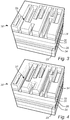
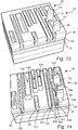
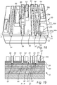
- FIGS 1-24 illustrate process flows of patterning methods.
- a method for patterning a target layer will now be described with reference to Figures 1-21 .
- the method will be described in connection with patterning a target layer 22 in the form of a hard mask layer, which in turn may be used for the purpose of patterning trenches in a dielectric layer stack 10. It is however noted that the method has a more general applicability for patterning trenches in any target layer, such as in a semiconductor a layer or a metal layer.
- FIG. 1 With reference to Figure 1 there is shown, in perspective, a section of a semiconductor structure or intermediate device.
- the structure may extend laterally or horizontally beyond the illustrated section.
- the illustrated planes of section extending through the structure are common to all the figures unless stated otherwise.
- the relative dimensions of the shown elements, in particular the relative thickness of the layers is merely schematic and may, for the purpose of illustrational clarity, differ from a physical structure.
- directions X and Y indicates a first and a second horizontal direction, respectively, (parallel to the main plane of extension of the layers) and Z indicates a vertical direction (normal to the main surface of the layers).
- the structure includes in a bottom-up direction a substrate 1, for instance a semiconductor substrate.
- An active device layer including semiconductor devices such as transistors may be fabricated on a main surface of the substrate 1.
- the active device layer may also be referred to as a front-end-of-line portion (FEOL-portion).
- a dielectric layer stack 10 is formed above the substrate 1.
- the dielectric layer stack 10 may comprise a low-k dielectric layer 12, an interface layer 14 and an oxide capping layer 16. More generally, the dielectric layer stack 10 may be of any conventional type used in back-end-of-line (BEOL) interconnect structures.
- BEOL back-end-of-line
- a layer stack 20 is formed above the dielectric layer stack 10.
- the layer stack 20 comprises in a bottom-up direction (i.e. parallel to the vertical direction Z) a target layer 22, a lower memorization layer 24 and an upper memorization layer 26.
- the memorization layers 24, 26 may through patterning be used to "memorize” or "store” one or more parts of a final pattern that is to be transferred to the target layer.
- the lower and upper memorization layers 24, 26 may be referred to as the lower and upper patterning layers 24, 26.
- the target layer 22 may be a TiN layer.
- the lower memorization layer 24 may be a SiN layer.
- the upper memorization layer 26 may be an a-Si layer.
- the target layer may be formed of a first material.
- the lower memorization layer may be formed of a second material different from the first material.
- the upper memorization layer may be formed of a third material different from the first material and the third material.
- Figures 2-5 illustrate process steps for forming a first mask layer 31 and forming a set of trenches 40 therein using lithography and etching.
- a first lithographic layer stack 30 has been formed on the layer stack 20.
- the lithographic layer stack 30 comprises the first mask layer 31 and a photoresist layer 38.
- the first mask layer 31 may for instance be formed by a carbon-based patterning film, for instance an amorphous carbon film, or some other conventional organic or non-organic patterning film allowing high-fidelity pattern transfer when used in a lithographic layer stack.
- the layer stack 30 may additionally comprise one or more transfer layers 32, 34, 36 intermediate the first mask layer 31 and the photoresist layer 38.
- the layer stack 30 may comprise an anti-reflective coating 32, for instance in the form of a silicon-including layer such as SiOC.
- the layer stack 30 may comprise an organic spin-on layer 34, such as a spin-on-carbon (SOC) layer.
- the layer stack may further comprise an additional anti-reflective coating 36, for instance in the form of a spin-on-glass (SOG) layer or a silicon-including layer.
- a trench pattern comprising a set of trenches 39 have been lithographically patterned in the photoresist layer 38.
- Each trench of the set of trenches 39 is formed over a region of the target layer 22 where a trench of a first set of target trenches 100 is to be formed.
- the trenches 39 may be formed with various widths (along the first horizontal direction X) and various longitudinal dimensions (along the second horizontal direction Y).
- the trenches 39 may extend in parallel to each other.
- the trench pattern comprising the set of trenches 39 have been transferred into the transfer layers 32 and 34 to form a set of trenches 35 therein.
- the pattern transfer may comprise first transferring the trench pattern comprising the set of trenches 39 into the transfer layer 36 by etching the layer 36 while using the photoresist layer 38 as an etch mask.
- the transfer layer 34 may then be etched through the trenches in the transfer layer 36. If the transfer layer 34 is formed by an organic material (such as a SOC), the photoresist layer 38 may be consumed during the etching. Thus, mainly the transfer layer 36 may act as an etch mask during the patterning of the transfer layer 34.
- the trenches 35 in the transfer layer 34 may then be further transferred into the transfer layer 32 by etching. During the etching the transfer layer 36 may be consumed. Thus, mainly the transfer layer 34 may act as an etch mask during the patterning of the transfer layer 32.
- Figure 4 illustrates an optional trimming step which may be performed prior to patterning the first mask layer 31.
- the patterned transfer layers 32, 34 may be subjected to a short isotropic etch step, trimming the lateral dimensions of the layers 32, 34 thus forming a trimmed trench pattern 37.
- the critical dimensions of the lithographically defined trench pattern may be reduced to the desired values prior to patterning the upper memorization layer 26. Consequently, the trimming results in increasing the widths of the trenches 35 to form the widened trenches 37 in the transfer layers 32, 34.
- the trimmed trench pattern 37 has been transferred into the first mask layer 31 to form a pattern comprising a set of trenches 40.
- the set of trenches 40 extend in parallel to each other.
- the set of trenches 40 exposes an upper surface of the upper memorization layer 26.
- the set of trenches 40 may be formed by etching the first mask layer 31 while using at least the transfer layer 32, possibly also the transfer layer 34 (depending on etch selectivities), as an etch mask.
- the lithographic layer stack 30 may comprise only the first mask layer 31 and the photoresist layer 38.
- the set of trenches 39 may be lithographically patterned in the photoresist layer 38.
- the set of trenches 40 may subsequently be patterned in the first mask layer 31 using the patterned photoresist layer 38 as an etch mask.
- the various steps of patterning the layer stack 30 may comprise using etching techniques which per se are known in the art. For instance, a SOG or SiOC layer may be etched using fluorine based etching chemistries (e.g. CF4, CH3F, CHF3, CH2F2, C4F8 or C4F6), a SOC or carbon-based patterning film may be etched using N 2 /H 2 or O 2 based etching chemistries (e.g. O 2 , CO 2 , SO 2 optionally supplemented with HBr or CH 4 ).
- fluorine based etching chemistries e.g. CF4, CH3F, CHF3, CH2F2, C4F8 or C4F6
- a SOC or carbon-based patterning film may be etched using N 2 /H 2 or O 2 based etching chemistries (e.g. O 2 , CO 2 , SO 2 optionally supplemented with HBr or CH 4 ).
- a set of upper trenches commonly referenced 44, have been patterned in the upper memorization layer 26.
- the set of upper trenches 44 comprises for instance trenches 46, 47 and 48.
- the set of upper trenches 44 extend in parallel to each other.
- the patterning may comprise etching the upper memorization layer 26 using the first mask layer as an etch mask.
- the pattern comprising the set of trenches 40 in first mask layer 31 have accordingly been memorized in the upper memorization layer 26.
- a conventional etching process preferably a dry etching process, compatible with the materials forming the first mask layer 31 and the upper memorization layer 26 may be used.
- an a-Si layer may be etched through an carbon-based etch mask using Cl 2 or fluorine-based etching chemistries such as SF 6 .
- a trimming step may be applied to upper memorization layer 26 subsequent to patterning the upper trenches 44 therein.
- the trimming may comprise oxidizing the upper memorization layer 26 to form an oxide layer covering the upper memorization layer 26 and thereafter removing the oxide layer from the upper memorization layer 26 in an etch step, for instance using dHF.
- This technique may be applied provided the upper memorization layer 26 is formed of a material which may be oxidized in a controlled manner, for instance a-Si.
- the spacer layer 50 may be an oxide layer, such as silicon oxide SiO 2 or a metal oxide layer such as titanium oxide TiOx.
- a SiN layer may also be used provided SiN is not used to form the lower memorization layer 24.
- the spacer layer 50 may be formed of a fourth material different from each one of the first through third materials forming the target layer 22, the lower memorization layer 24 and the upper memorization layer 26.
- the spacer layer 50 may be formed by depositing a conformal spacer layer covering the patterned upper memorization layer 26, for instance in an atomic layer deposition (ALD) process.
- ALD atomic layer deposition
- a vertical anisotropic etch may then be performed such that portions of the conformally deposited spacer layer on horizontally oriented surfaces are removed, while portions deposited on the vertically oriented sidewalls of the upper trenches 44 are preserved to form the final spacer layer 50.
- the spacer layer 50 thus defines a pair of spacer lines extending along each upper trench 44, such as spacer lines 50a, 50b along the upper trench 47 and spacer lines 50c, 50d along the upper trench 48.
- the spacer layer 50 may also form on end walls of the trenches 44. The end wall portions layer 50 accordingly connect the spacer lines 50a, 50b and 50c, 50d formed on the mutually opposite trench sidewalls.
- Figure 8-9 illustrate forming of a first block pattern 58 above the lower memorization layer 24.
- the first block pattern 58 comprises a set of first blocks 60, 62. Each first block 60, 62 extends across an upper trench 46, 48 in the upper memorization layer 26.
- a first block mask layer 52 has been formed to cover the patterned upper memorization layer 26.
- the first block mask layer 52 may be formed by a SOC layer or some other organic spin-on layer.
- a photoresist layer has been formed above the first block mask layer 52 and lithographically patterned to define a photoresist block mask comprising a set of resist blocks 54, 56. Each resist block 54, 56 extends across an upper trench 46, 47 in the upper memorization layer 26 (c.f. Figure 7 ).
- the first block mask layer 52 has been patterned to form the first block pattern 58.
- the patterning may comprise etching the first block mask layer 52 using the photoresist block mask 54, 56 as an etch mask. Accordingly, a set of first blocks 60, 62 may be patterned in the first block mask layer 52. Following pattering of the first block mask layer 52, the resist blocks 54, 56 may be stripped from the first blocks 60, 62. Similar to the patterning of the first mask layer 31, the patterning of the first block mask layer 52 may comprise a number of transfer steps into one or more transfer layers intermediate the layers 52 and the photoresist layer (such as anti-reflective coating(s) of SOG and/or SiOC or another silicon-including layer).
- a first set of lower trenches have been patterned in the lower memorization layer 24 and comprising for instance trenches 66, 67, 68.
- the patterning may comprise etching the lower memorization layer 24 while using the patterned upper memorization layer 26, the spacer layer 50 and the first block pattern 58 as an etch mask.
- the first lower trenches 64 exposes an upper surface of the target layer 22.
- An etching process preferably a dry etching process, allowing etching of the lower memorization layer 24 selectively to the first blocks 60, 62, the spacer layer 50 and the upper memorization layer 26 may be used.
- a SiN layer may be etched selectively to SOC, a-Si and an oxide such as a silicon or metal oxide (e.g. SiO 2 or TiO x ) using fluorine-based etching chemistries.
- first lower trenches 64 such as first lower trenches 66, 67 are interrupted by a respective trench interruption.
- the trench interruptions are formed by the portions 24a, 24b of the lower memorization layer 24 preserved under the first blocks 60, 62.
- the trench 66 forms an interrupted or discontinuous trench formed by two trench portions 66a, 66b.
- the trench 67 forms an interrupted or discontinuous trench formed by two trench portions 67a, 67b.
- interrupted trenches with more relaxed tip-to-tip separation may be formed without relying on a block-based technique, i.e. by being directly lithographically defined and etched into the first mask layer 31.
- Figure 12-14 illustrate forming of a second block pattern 82 above the (once) patterned lower memorization layer 24.
- the second block pattern 82 is formed by again patterning the (already once patterned) upper memorization layer 26.
- the second block pattern 82 comprises a set of second blocks 26a, 26b, each second block being formed by a respective portion 26a, 26b of the upper memorization layer 26 remaining after the second block patterning.
- a second block mask layer 70 has been formed to cover the patterned lower and upper memorization layers 24, 26.
- the second block mask layer 70 fills the first set of lower trenches 64 in the lower memorization layer 24 and the upper trenches 44 in the upper memorization layer 26.
- the second block mask layer 70 may be formed by a SOC layer or some other organic spin-on layer.
- a photoresist layer has been formed above the second block mask layer 70 and lithographically patterned to define a photoresist block mask comprising a set of resist blocks 72, 74. Each resist block 72, 74 is formed over a respective portion 26a, 26b of the upper memorization layer 26.
- the second block mask layer 70 has been patterned to form a second block mask 78.
- the second block mask 78 comprises a set of second mask blocks 79, 80.
- the patterning may comprise etching the second block layer 70 using the photoresist block mask 72, 74 as an etch mask. The etching may be stopped when the upper surface of the target layer 22 is exposed in the lower trenches 64. Accordingly, following the patterning of the second block mask layer 70, the upper surface of the target layer 22 is again exposed in the lower trenches 64 in the lower memorization layer.
- the patterning of the second block mask layer 70 may proceed in a similar fashion as the above described patterning of the first block mask layer 52.
- the (once patterned) upper memorization layer 26 has been patterned to form the second block pattern 82.
- the patterning may comprise etching the remaining portions of the upper memorization layer 26 using the second block mask 78 as an etch mask.
- the second block pattern 82 is formed by the portions 26a, 26b of the upper memorization layer 26 preserved under the second mask blocks 79, 78.
- the resist blocks 79, 78 may be stripped from the second blocks 26a, 26b.
- the upper memorization layer 26 may be etched using any of the etching chemistries discussed in connection with the first patterning of the upper memorization layer 26.
- a first set of target trenches have been patterned in the target layer 22 under the first set of lower trenches 64.
- the first set of lower trenches 64 exposes an upper surfaces of an underlying layer, i.e. in the illustrated process flow formed by an upper surface of the dielectric layer stack 10.
- the first set of target trenches 100 correspond to the first set of lower trenches 64.
- the first set of target trenches 100 extend in parallel to each other.
- the first set of target trenches 100 comprises for instance first target trenches 102 and 104.
- the first target trench 102 is formed by two trench portions 102a, and 102b interrupted by a trench interruption formed by a portion of the target layer 22 preserved under the portion 24b of the lower memorization layer 24.
- the patterning of the first set of target trenches 100 may comprise etching the target layer 22 through the first set of lower trenches 64 in the lower memorization layer 26. Accordingly, the (once) patterned lower memorization layer 26 and the spacer layer 50 may be used as a combined etch mask during the patterning of the target layer 22.
- the etching may advantageously be tuned such that the second block mask 78 and/or at least the second block pattern 82 are at least partially preserved following formation of the first set of target trenches 100.
- the first set of target trenches 100 and the upper memorization layer 26 may be etched simultaneously, i.e. by the same etching chemistry, and selectively to the spacer layer 50 and the lower memorization layer 24.
- a-Si and TiN may be etched simultaneously and selectively to an oxide such as a silicon or metal oxide (e.g. SiO 2 or TiO x ) and SiN using an Cl 2 -based etching chemistry.
- the second block mask 78 (or remaining portions thereof) may be removed from the second block pattern 82 by etching. The resulting structure is shown in figure 15 .
- Figures 16-17 illustrate process steps for forming a second mask layer 86 and forming a set of trenches 92 therein using lithography and etching.
- a second lithographic layer stack 84 has been formed above the patterned lower memorization layer 24 and the second block pattern 82.
- the lithographic layer stack 84 comprises the second mask layer 86 and a photoresist layer 90.
- the second mask layer 86 may be formed by a SOC layer or some other organic spin-on-layer.
- the layer stack 30 may additionally comprise one or more transfer layers 88 intermediate the second mask layer 86 and the photoresist layer 90, such as an anti-reflective coating, for instance of SOG or SiOC.
- a trench pattern comprising a set of trenches 91 have been lithographically patterned in the photoresist layer 90.
- Each trench of the set of trenches 91 is formed over a respective remaining portion of the (once patterned) lower memorization layer 24.
- each trench of the set of trenches 91 is formed over a region of the target layer 22 where a trench of a second set of target trenches 106 is to be formed.
- the trenches 91 may be formed with various widths (along the first horizontal direction X) and various longitudinal dimensions (along the second horizontal direction Y).
- the trenches 39 may extend in parallel to each other.
- the trenches 39 may further extend in parallel to the first set of lower trenches 64 already formed in the lower memorization layer 24.
- the trench pattern comprising the set of trenches 91 have been transferred into the transfer layer 88 and the second mask layer 86 to form a set of trenches 92.
- the set of trenches 92 comprises for instance trenches 93, 94.
- the set of trenches 92 exposes an upper surface of the remaining portions of the (once patterned) lower memorization layer 24.
- At least a subset of the trenches 92, such as trenches 93, 94 may be formed to expose and extend along one or more spacer lines 50b, 50c, 50d.
- At least a subset of the trenches, such as the trench 94 may be formed to expose one or more second blocks 26a, 26b of the second block pattern 82.
- the pattern transfer may comprise first transferring the trench pattern comprising the set of trenches 91 into the transfer layer 88 by etching the layer 88 while using the photoresist layer 90 as an etch mask.
- the second mask layer 86 may then be etched through the trenches in the transfer layer 88. If the second mask layer 86 is formed by an organic material, the photoresist layer 90 may be consumed during the etching.
- the SOG transfer layer 88 may act as an etch mask during the patterning of the second mask layer 86.
- trimming of the trench pattern may be performed, analogous to the trimming of the trenches in the mask layer stack 30.
- a second set of lower trenches 96 have been patterned in the (once patterned) lower memorization layer 24.
- the patterning may comprise etching the lower memorization layer 24 using the second mask layer 86, the spacer layer 50 and the second block pattern 82 as an etch mask.
- the second set of lower trenches 96 exposes an upper surface of the (once patterned) target layer 22. Any of the etching processes mentioned in connection with the patterning of the first set of lower trenches 64 may be used for etching the second set of lower trenches 96.
- the second lower trenches 96 are interrupted by one or more trench interruptions 24c, 24d, each trench interruption 24c, 24d being formed by a portion 24c, 24d of the lower memorization layer 24 preserved under a respective one of said second blocks 78, 80.
- the trench 98 forms an interrupted or discontinuous trench formed by three trench portions 98a, 98b, 98c.
- Figure 19 is a plan view along line A-A indicated in figure 18 , showing more clearly the alternating arrangement of the first set of lower trenches 64 and the second set of lower trenches 96.
- the trenches 67, 68 of the first set of lower trenches 64 and the trenches 97, 98 of the second set of lower trenches 96 are arranged alternatingly.
- Each trench of this subset of trenches 67, 68, 97, 98 is separated from a neighboring one of this subset by a distance defined by the thickness of the spacer layer 50.
- a second set of target trenches 106 have been patterned in the target layer 22 under the second set of lower trenches 96.
- the second set of target trenches 106 exposes an upper surfaces of the underlying layer, i.e. in the illustrated process flow formed by the upper surface of the dielectric layer stack 10.
- the target trenches 102, 104 of the first set 100 and the target trenches 108, 110 of the second set 106 forms a subset of target trenches which are arranged alternatingly.
- Each trench of this subset of trenches 67, 68, 97, 98 is separated from a neighboring one of this subset by a distance defined by the thickness of the spacer layer 50.
- the patterning of the second set of target trenches 106 may comprise etching the target layer 22 through the second set of lower trenches 96 in the lower memorization layer 26. Accordingly, the (twice) patterned lower memorization layer 26 and the spacer layer 50 may be used as a combined etch mask during the second patterning of the target layer 22. Any of the etching processes mentioned in connection with the patterning of the first set of target trenches 100 may be used for etching the second set of target trenches 106.
- the remaining portions of the lower memorization layer 26 and the spacer layer 50 may be removed from the patterned target layer 22 by etching.
- the resulting structure is shown in figure 21 .
- the method may then proceed with patterning the dielectric layer stack 10 using the target layer 22 as an etch mask to form a set of trenches in the dielectric layer.
- the dielectric layer trenches may subsequently be filled with a conductive material to form a pattern of conductive paths of an interconnect structure.
- the first and second sets of target trenches 100, 106 in the target layer 22 may instead of being patterned in a sequential approach, be patterned simultaneously:
- the alternative process may proceed as disclosed with reference to Figures 1-12 above.
- the second block mask layer 70 has accordingly been formed to cover the patterned lower and upper memorization layers 24, 26 and accordingly fill the first set of lower trenches 64.
- the patterning of the second block mask layer 70 may comprises etching the second block mask layer 70 to form the second block mask 78 comprising the set of second mask blocks 79, 80 and such that portions 170 of the second block mask layer 70 remain in the first set of lower trenches 64 of the lower memorization layer 24.
- the etching of the second block mask layer 70 may be stopped when an upper surface of the patterned upper memorization layer 26 is exposed. A thickness portion of the second block mask layer 70 may accordingly remain also in regions exposed by the resist block mask 72, 74, thereby forming the portions 170 filling the first set of lower trenches 64.
- the (once) patterned upper memorization layer 26 has been patterned to form the second block pattern 82 comprising second blocks 26a, 26b.
- the patterning may, like in Figure 14 , comprise etching the remaining portions of the upper memorization layer 26 using the second block mask 78 as an etch mask.
- the portions 170 of the second block mask layer 70 remaining in the first set of lower trenches 64 may mask the target layer 22, thus counteracting etching of the target layer 22 through the first set of lower trenches 64.
- the second block mask 78 and the portions of the second block mask layer 70 have been removed subsequent to forming the second block pattern 82.
- the target layer 22 is thereby exposed in the first set of lower trenches 64.
- the process may thereafter proceed in the manner disclosed in connection with figures 16-17 (forming the second mask layer 86 and the set of trenches 92), figure 18 (patterning the second set of lower trenches 96 in the lower memorization layer 24).
- the first and second set of target trenches 100, 106 may be patterned simultaneously in the target layer 22 by etching the target layer 22 and using the (twice) patterned lower memorization layer 24 as an etch mask.
- the remaining portions of the lower memorization layer 26 and the spacer layer 50 may be removed from the patterned target layer 22 by etching to arrive at the resulting structure shown in figure 21 .
Landscapes
- Physics & Mathematics (AREA)
- General Physics & Mathematics (AREA)
- Semiconductor Memories (AREA)
- Drying Of Semiconductors (AREA)
Priority Applications (3)
| Application Number | Priority Date | Filing Date | Title |
|---|---|---|---|
| EP18191776.6A EP3618103A1 (de) | 2018-08-30 | 2018-08-30 | Strukturierungsmethode |
| CN201910540801.XA CN110874019B (zh) | 2018-08-30 | 2019-06-21 | 一种图案化方法 |
| US16/556,124 US10770295B2 (en) | 2018-08-30 | 2019-08-29 | Patterning method |
Applications Claiming Priority (1)
| Application Number | Priority Date | Filing Date | Title |
|---|---|---|---|
| EP18191776.6A EP3618103A1 (de) | 2018-08-30 | 2018-08-30 | Strukturierungsmethode |
Publications (1)
| Publication Number | Publication Date |
|---|---|
| EP3618103A1 true EP3618103A1 (de) | 2020-03-04 |
Family
ID=63490225
Family Applications (1)
| Application Number | Title | Priority Date | Filing Date |
|---|---|---|---|
| EP18191776.6A Withdrawn EP3618103A1 (de) | 2018-08-30 | 2018-08-30 | Strukturierungsmethode |
Country Status (3)
| Country | Link |
|---|---|
| US (1) | US10770295B2 (de) |
| EP (1) | EP3618103A1 (de) |
| CN (1) | CN110874019B (de) |
Cited By (3)
| Publication number | Priority date | Publication date | Assignee | Title |
|---|---|---|---|---|
| EP3901987A1 (de) | 2020-04-23 | 2021-10-27 | IMEC vzw | Musterverfahren |
| EP3901986A1 (de) | 2020-04-23 | 2021-10-27 | IMEC vzw | Musterverfahren |
| US20220223415A1 (en) * | 2021-01-14 | 2022-07-14 | Imec Vzw | Patterning method |
Families Citing this family (3)
| Publication number | Priority date | Publication date | Assignee | Title |
|---|---|---|---|---|
| TW201921498A (zh) * | 2017-09-27 | 2019-06-01 | 美商微材料有限責任公司 | 選擇性氧化鋁蝕刻的使用 |
| KR102889699B1 (ko) | 2021-04-06 | 2025-11-24 | 삼성전자주식회사 | 반도체 소자의 제조방법 |
| US12148617B2 (en) | 2021-11-01 | 2024-11-19 | International Business Machines Corporation | Structure and method to pattern pitch lines |
Citations (4)
| Publication number | Priority date | Publication date | Assignee | Title |
|---|---|---|---|---|
| US20150200096A1 (en) * | 2014-01-14 | 2015-07-16 | Taiwan Semiconductor Manufacturing Co., Ltd. | Cut last self-aligned litho-etch patterning |
| WO2017083528A1 (en) * | 2015-11-12 | 2017-05-18 | Qualcomm Incorporated | Self-aligned metal cut and via in semiconductor back-end-of-line (beol) processing, and related apparatus |
| EP3255663A1 (de) * | 2016-06-07 | 2017-12-13 | IMEC vzw | Verfahren zur unterbrechung einer leitung in einer elektronischen verbindung |
| US20180114721A1 (en) * | 2016-10-20 | 2018-04-26 | Tokyo Electron Limited | Method of Reducing Overlay Error in Via to Grid Patterning |
Family Cites Families (19)
| Publication number | Priority date | Publication date | Assignee | Title |
|---|---|---|---|---|
| US4639288A (en) * | 1984-11-05 | 1987-01-27 | Advanced Micro Devices, Inc. | Process for formation of trench in integrated circuit structure using isotropic and anisotropic etching |
| JP3296324B2 (ja) * | 1999-04-07 | 2002-06-24 | 日本電気株式会社 | 半導体メモリ装置の製造方法 |
| KR100586165B1 (ko) * | 2003-12-30 | 2006-06-07 | 동부일렉트로닉스 주식회사 | 바닥 반사 방지 코팅 방법 |
| JP4707593B2 (ja) * | 2006-03-23 | 2011-06-22 | 大日本スクリーン製造株式会社 | 熱処理装置と基板吸着方法 |
| US20080113157A1 (en) * | 2006-11-13 | 2008-05-15 | Seagate Technology Llc | Method for fabricating master stamper/imprinters for patterned recording media utilizing hybrid resist |
| KR101284746B1 (ko) * | 2006-12-26 | 2013-07-16 | 주식회사 케이씨텍 | 포토레지스트 도포 노즐의 처짐 방지장치 |
| US20110079918A1 (en) * | 2009-10-01 | 2011-04-07 | Applied Materials, Inc. | Plasma-based organic mask removal with silicon fluoride |
| US8629040B2 (en) | 2011-11-16 | 2014-01-14 | Taiwan Semiconductor Manufacturing Company, Ltd. | Methods for epitaxially growing active regions between STI regions |
| WO2014005841A1 (en) * | 2012-07-03 | 2014-01-09 | Imec | A method for fabricating a thin film transistor |
| US9466486B2 (en) | 2013-08-30 | 2016-10-11 | Taiwan Semiconductor Manufacturing Company, Ltd. | Method for integrated circuit patterning |
| CN107112212B (zh) * | 2014-12-22 | 2021-03-12 | 东京毅力科创株式会社 | 使用接枝聚合物材料图案化基底 |
| JP6715415B2 (ja) * | 2016-01-29 | 2020-07-01 | 東京エレクトロン株式会社 | メモリフィンパターンを形成するための方法及びシステム |
| US9679809B1 (en) | 2016-03-22 | 2017-06-13 | Globalfoundries Inc. | Method of forming self aligned continuity blocks for mandrel and non-mandrel interconnect lines |
| US9818623B2 (en) | 2016-03-22 | 2017-11-14 | Globalfoundries Inc. | Method of forming a pattern for interconnection lines and associated continuity blocks in an integrated circuit |
| US9786545B1 (en) * | 2016-09-21 | 2017-10-10 | Globalfoundries Inc. | Method of forming ANA regions in an integrated circuit |
| US9852986B1 (en) | 2016-11-28 | 2017-12-26 | Globalfoundries Inc. | Method of patterning pillars to form variable continuity cuts in interconnection lines of an integrated circuit |
| US9941164B1 (en) * | 2016-12-05 | 2018-04-10 | Samsung Electronics Co., Ltd. | Self-aligned block patterning with density assist pattern |
| US9812351B1 (en) | 2016-12-15 | 2017-11-07 | Globalfoundries Inc. | Interconnection cells having variable width metal lines and fully-self aligned continuity cuts |
| EP3367429A1 (de) * | 2017-02-27 | 2018-08-29 | IMEC vzw | Verfahren zur definition von patterns für leiterbahnen in einer dielektrischen schicht |
-
2018
- 2018-08-30 EP EP18191776.6A patent/EP3618103A1/de not_active Withdrawn
-
2019
- 2019-06-21 CN CN201910540801.XA patent/CN110874019B/zh active Active
- 2019-08-29 US US16/556,124 patent/US10770295B2/en active Active
Patent Citations (4)
| Publication number | Priority date | Publication date | Assignee | Title |
|---|---|---|---|---|
| US20150200096A1 (en) * | 2014-01-14 | 2015-07-16 | Taiwan Semiconductor Manufacturing Co., Ltd. | Cut last self-aligned litho-etch patterning |
| WO2017083528A1 (en) * | 2015-11-12 | 2017-05-18 | Qualcomm Incorporated | Self-aligned metal cut and via in semiconductor back-end-of-line (beol) processing, and related apparatus |
| EP3255663A1 (de) * | 2016-06-07 | 2017-12-13 | IMEC vzw | Verfahren zur unterbrechung einer leitung in einer elektronischen verbindung |
| US20180114721A1 (en) * | 2016-10-20 | 2018-04-26 | Tokyo Electron Limited | Method of Reducing Overlay Error in Via to Grid Patterning |
Cited By (7)
| Publication number | Priority date | Publication date | Assignee | Title |
|---|---|---|---|---|
| EP3901987A1 (de) | 2020-04-23 | 2021-10-27 | IMEC vzw | Musterverfahren |
| EP3901986A1 (de) | 2020-04-23 | 2021-10-27 | IMEC vzw | Musterverfahren |
| US11476155B2 (en) | 2020-04-23 | 2022-10-18 | Imec Vzw | Patterning method |
| US11710637B2 (en) | 2020-04-23 | 2023-07-25 | Imec Vzw | Patterning method |
| US20220223415A1 (en) * | 2021-01-14 | 2022-07-14 | Imec Vzw | Patterning method |
| EP4030465A1 (de) | 2021-01-14 | 2022-07-20 | Imec VZW | Musterverfahren |
| US12261045B2 (en) | 2021-01-14 | 2025-03-25 | Imec Vzw | Patterning method |
Also Published As
| Publication number | Publication date |
|---|---|
| US10770295B2 (en) | 2020-09-08 |
| US20200075335A1 (en) | 2020-03-05 |
| CN110874019A (zh) | 2020-03-10 |
| CN110874019B (zh) | 2023-04-28 |
Similar Documents
| Publication | Publication Date | Title |
|---|---|---|
| US10770295B2 (en) | Patterning method | |
| US10840097B2 (en) | Semiconductor methods and devices | |
| CN110739210B (zh) | 半导体结构及其形成方法 | |
| US10192956B2 (en) | Method for producing fin structures of a semiconductor device in a substrate | |
| TWI391988B (zh) | 利用間距減縮製造裝置之方法及相關結構 | |
| KR101091298B1 (ko) | 반도체 디바이스의 임계 치수를 축소하는 방법 및 축소된 임계 치수를 갖는 부분적으로 제조된 반도체 디바이스 | |
| JP4953740B2 (ja) | 半導体素子のストレージノードコンタクトプラグの形成方法 | |
| US9123659B1 (en) | Method for manufacturing finFET device | |
| CN111524855B (zh) | 半导体结构及其形成方法 | |
| CN108807152A (zh) | 半导体装置的形成方法 | |
| US10147637B2 (en) | Methods for forming conductive paths and vias | |
| CN110690117A (zh) | 半导体结构及其形成方法 | |
| US20180247814A1 (en) | Method for Defining Patterns for Conductive Paths in a Dielectric Layer | |
| US10651076B2 (en) | Method for defining patterns for conductive paths in dielectric layer | |
| KR20090070103A (ko) | 반도체 소자의 패턴 형성 방법 | |
| US12261045B2 (en) | Patterning method | |
| CN108511388B (zh) | 使目标层图案化的方法 | |
| US11710637B2 (en) | Patterning method | |
| US11476155B2 (en) | Patterning method | |
| CN112951724A (zh) | 半导体结构及其形成方法 | |
| US20250079174A1 (en) | Method for processing a substrate |
Legal Events
| Date | Code | Title | Description |
|---|---|---|---|
| PUAI | Public reference made under article 153(3) epc to a published international application that has entered the european phase |
Free format text: ORIGINAL CODE: 0009012 |
|
| STAA | Information on the status of an ep patent application or granted ep patent |
Free format text: STATUS: THE APPLICATION HAS BEEN PUBLISHED |
|
| AK | Designated contracting states |
Kind code of ref document: A1 Designated state(s): AL AT BE BG CH CY CZ DE DK EE ES FI FR GB GR HR HU IE IS IT LI LT LU LV MC MK MT NL NO PL PT RO RS SE SI SK SM TR |
|
| AX | Request for extension of the european patent |
Extension state: BA ME |
|
| STAA | Information on the status of an ep patent application or granted ep patent |
Free format text: STATUS: THE APPLICATION IS DEEMED TO BE WITHDRAWN |
|
| 18D | Application deemed to be withdrawn |
Effective date: 20200905 |