EP3618111A1 - Ensemble de boîtiers à del et ampoule à del comprenant ce dernier - Google Patents
Ensemble de boîtiers à del et ampoule à del comprenant ce dernier Download PDFInfo
- Publication number
- EP3618111A1 EP3618111A1 EP18809817.2A EP18809817A EP3618111A1 EP 3618111 A1 EP3618111 A1 EP 3618111A1 EP 18809817 A EP18809817 A EP 18809817A EP 3618111 A1 EP3618111 A1 EP 3618111A1
- Authority
- EP
- European Patent Office
- Prior art keywords
- led package
- led
- light
- package
- chip
- Prior art date
- Legal status (The legal status is an assumption and is not a legal conclusion. Google has not performed a legal analysis and makes no representation as to the accuracy of the status listed.)
- Granted
Links
Images



Classifications
-
- H—ELECTRICITY
- H10—SEMICONDUCTOR DEVICES; ELECTRIC SOLID-STATE DEVICES NOT OTHERWISE PROVIDED FOR
- H10H—INORGANIC LIGHT-EMITTING SEMICONDUCTOR DEVICES HAVING POTENTIAL BARRIERS
- H10H29/00—Integrated devices, or assemblies of multiple devices, comprising at least one light-emitting semiconductor element covered by group H10H20/00
- H10H29/10—Integrated devices comprising at least one light-emitting semiconductor component covered by group H10H20/00
- H10H29/14—Integrated devices comprising at least one light-emitting semiconductor component covered by group H10H20/00 comprising multiple light-emitting semiconductor components
-
- H—ELECTRICITY
- H10—SEMICONDUCTOR DEVICES; ELECTRIC SOLID-STATE DEVICES NOT OTHERWISE PROVIDED FOR
- H10W—GENERIC PACKAGES, INTERCONNECTIONS, CONNECTORS OR OTHER CONSTRUCTIONAL DETAILS OF DEVICES COVERED BY CLASS H10
- H10W90/00—Package configurations
-
- F—MECHANICAL ENGINEERING; LIGHTING; HEATING; WEAPONS; BLASTING
- F21—LIGHTING
- F21K—NON-ELECTRIC LIGHT SOURCES USING LUMINESCENCE; LIGHT SOURCES USING ELECTROCHEMILUMINESCENCE; LIGHT SOURCES USING CHARGES OF COMBUSTIBLE MATERIAL; LIGHT SOURCES USING SEMICONDUCTOR DEVICES AS LIGHT-GENERATING ELEMENTS; LIGHT SOURCES NOT OTHERWISE PROVIDED FOR
- F21K9/00—Light sources using semiconductor devices as light-generating elements, e.g. using light-emitting diodes [LED] or lasers
-
- F—MECHANICAL ENGINEERING; LIGHTING; HEATING; WEAPONS; BLASTING
- F21—LIGHTING
- F21K—NON-ELECTRIC LIGHT SOURCES USING LUMINESCENCE; LIGHT SOURCES USING ELECTROCHEMILUMINESCENCE; LIGHT SOURCES USING CHARGES OF COMBUSTIBLE MATERIAL; LIGHT SOURCES USING SEMICONDUCTOR DEVICES AS LIGHT-GENERATING ELEMENTS; LIGHT SOURCES NOT OTHERWISE PROVIDED FOR
- F21K9/00—Light sources using semiconductor devices as light-generating elements, e.g. using light-emitting diodes [LED] or lasers
- F21K9/20—Light sources comprising attachment means
- F21K9/23—Retrofit light sources for lighting devices with a single fitting for each light source, e.g. for substitution of incandescent lamps with bayonet or threaded fittings
-
- F—MECHANICAL ENGINEERING; LIGHTING; HEATING; WEAPONS; BLASTING
- F21—LIGHTING
- F21K—NON-ELECTRIC LIGHT SOURCES USING LUMINESCENCE; LIGHT SOURCES USING ELECTROCHEMILUMINESCENCE; LIGHT SOURCES USING CHARGES OF COMBUSTIBLE MATERIAL; LIGHT SOURCES USING SEMICONDUCTOR DEVICES AS LIGHT-GENERATING ELEMENTS; LIGHT SOURCES NOT OTHERWISE PROVIDED FOR
- F21K9/00—Light sources using semiconductor devices as light-generating elements, e.g. using light-emitting diodes [LED] or lasers
- F21K9/20—Light sources comprising attachment means
- F21K9/23—Retrofit light sources for lighting devices with a single fitting for each light source, e.g. for substitution of incandescent lamps with bayonet or threaded fittings
- F21K9/235—Details of bases or caps, i.e. the parts that connect the light source to a fitting; Arrangement of components within bases or caps
-
- H—ELECTRICITY
- H10—SEMICONDUCTOR DEVICES; ELECTRIC SOLID-STATE DEVICES NOT OTHERWISE PROVIDED FOR
- H10H—INORGANIC LIGHT-EMITTING SEMICONDUCTOR DEVICES HAVING POTENTIAL BARRIERS
- H10H20/00—Individual inorganic light-emitting semiconductor devices having potential barriers, e.g. light-emitting diodes [LED]
- H10H20/80—Constructional details
- H10H20/81—Bodies
- H10H20/822—Materials of the light-emitting regions
- H10H20/824—Materials of the light-emitting regions comprising only Group III-V materials, e.g. GaP
- H10H20/825—Materials of the light-emitting regions comprising only Group III-V materials, e.g. GaP containing nitrogen, e.g. GaN
-
- H—ELECTRICITY
- H10—SEMICONDUCTOR DEVICES; ELECTRIC SOLID-STATE DEVICES NOT OTHERWISE PROVIDED FOR
- H10H—INORGANIC LIGHT-EMITTING SEMICONDUCTOR DEVICES HAVING POTENTIAL BARRIERS
- H10H20/00—Individual inorganic light-emitting semiconductor devices having potential barriers, e.g. light-emitting diodes [LED]
- H10H20/80—Constructional details
- H10H20/83—Electrodes
-
- H—ELECTRICITY
- H10—SEMICONDUCTOR DEVICES; ELECTRIC SOLID-STATE DEVICES NOT OTHERWISE PROVIDED FOR
- H10H—INORGANIC LIGHT-EMITTING SEMICONDUCTOR DEVICES HAVING POTENTIAL BARRIERS
- H10H20/00—Individual inorganic light-emitting semiconductor devices having potential barriers, e.g. light-emitting diodes [LED]
- H10H20/80—Constructional details
- H10H20/85—Packages
- H10H20/851—Wavelength conversion means
-
- H—ELECTRICITY
- H10—SEMICONDUCTOR DEVICES; ELECTRIC SOLID-STATE DEVICES NOT OTHERWISE PROVIDED FOR
- H10H—INORGANIC LIGHT-EMITTING SEMICONDUCTOR DEVICES HAVING POTENTIAL BARRIERS
- H10H20/00—Individual inorganic light-emitting semiconductor devices having potential barriers, e.g. light-emitting diodes [LED]
- H10H20/80—Constructional details
- H10H20/85—Packages
- H10H20/851—Wavelength conversion means
- H10H20/8511—Wavelength conversion means characterised by their material, e.g. binder
- H10H20/8512—Wavelength conversion materials
-
- F—MECHANICAL ENGINEERING; LIGHTING; HEATING; WEAPONS; BLASTING
- F21—LIGHTING
- F21Y—INDEXING SCHEME ASSOCIATED WITH SUBCLASSES F21K, F21L, F21S and F21V, RELATING TO THE FORM OR THE KIND OF THE LIGHT SOURCES OR OF THE COLOUR OF THE LIGHT EMITTED
- F21Y2113/00—Combination of light sources
- F21Y2113/10—Combination of light sources of different colours
- F21Y2113/13—Combination of light sources of different colours comprising an assembly of point-like light sources
-
- F—MECHANICAL ENGINEERING; LIGHTING; HEATING; WEAPONS; BLASTING
- F21—LIGHTING
- F21Y—INDEXING SCHEME ASSOCIATED WITH SUBCLASSES F21K, F21L, F21S and F21V, RELATING TO THE FORM OR THE KIND OF THE LIGHT SOURCES OR OF THE COLOUR OF THE LIGHT EMITTED
- F21Y2115/00—Light-generating elements of semiconductor light sources
- F21Y2115/10—Light-emitting diodes [LED]
-
- H—ELECTRICITY
- H10—SEMICONDUCTOR DEVICES; ELECTRIC SOLID-STATE DEVICES NOT OTHERWISE PROVIDED FOR
- H10H—INORGANIC LIGHT-EMITTING SEMICONDUCTOR DEVICES HAVING POTENTIAL BARRIERS
- H10H20/00—Individual inorganic light-emitting semiconductor devices having potential barriers, e.g. light-emitting diodes [LED]
- H10H20/80—Constructional details
- H10H20/85—Packages
- H10H20/857—Interconnections, e.g. lead-frames, bond wires or solder balls
Definitions
- Embodiments of the present invention relate to an LED package set and an LED bulb including the same.
- incandescent lamps using filaments have been widely used as luminaires.
- operation of a filament-based incandescent lamp is based on the principle that light is obtained by temperature radiation caused by heating a tungsten filament in a vacuum glass bulb to high temperature through application of electricity.
- Such a typical incandescent lamp is not suitable for long-term use due to short lifespan of the filament and has extremely low energy efficiency since most of energy supplied thereto is released as heat and only a fraction of the energy is converted into light.
- LEDs light emitting diodes having long lifespan and high energy efficiency are used in luminaires.
- Embodiments of the present invention provide an LED package set which has high economic efficiency due to long lifespan and low heat generation thereof, and an LED bulb including the same.
- Embodiments of the present invention provide an LED package set which allows regulation of color temperature of light emitted therefrom, and an LED bulb including the same.
- Embodiments of the present invention provide an LED package set which can evenly emit light in all directions by emitting light in different directions, and an LED bulb including the same.
- an LED package set including: a substrate; a first LED package disposed on the substrate and including at least one first LED chip; a second LED package disposed on the substrate and including at least one second LED chip; and a resistor disposed on the substrate, the resistor being connected in series to the first LED package and connected in parallel to the second LED package.
- the second LED package is connected in parallel to the first LED package and the resistor. The first LED package and the second LED package emit light having different color temperatures.
- an LED bulb including: a base formed with an external electrode pad receiving electricity from an external power supply; an LED package set; a holder coupled to the LED package set; and a light transmissive cover enclosing the LED package set and coupled at one end thereof to the base.
- the LED package set includes a substrate having a pair of electrode pads formed at one end thereof, a first LED package including at least one first LED chip, a second LED package including at least one second LED chip, and a resistor.
- the holder is formed with a connection portion receiving one end of the LED package set and electrically connected to the pair of electrode pads of the substrate.
- the first LED package, the second LED package, and the resistor are disposed on the substrate.
- the first LED package and the second LED package are connected in parallel to one another and emit light having different color temperatures.
- the resistor is connected in series to the first LED package and connected in parallel to the second LED package.
- an LED package set and an LED bulb including the same can have long lifespan and low heat generation by employing an LED package instead of a tungsten filament, thereby improving economic efficiency.
- the LED package set and the LED bulb including the same can emit light having a suitable color temperature according to an environment using at least two LED packages emitting light having different color temperatures.
- the LED package set and the LED bulb including the same include a resistor connected in series to one LED package and connected in parallel to the other LED package.
- the LED package set and the LED bulb can emit light changed in color temperature with change in voltage and current supplied to the LED package set.
- an LED package set includes: a substrate; a first LED package disposed on the substrate and including at least one first LED chip; a second LED package disposed on the substrate and including at least one second LED chip; and a resistor disposed on the substrate, the resistor being connected in series to the first LED package and connected in parallel to the second LED package.
- the second LED package is connected in parallel to the first LED package and the resistor. The first LED package and the second LED package emit light having different color temperatures.
- the LED package set is driven in a constant current mode. Electricity applied to the LED package set is changed according to a dimming signal. According to the present invention, as voltage applied to the LED package set is changed according to the dimming signal, a current distribution ratio between the first LED package and the second LED package is changed. As a result, a color temperature of mixed light composed of light emitted from the first LED package and light emitted from the second LED package is changed.
- the substrate includes a pair of electrode pads formed thereon. One end of the first LED package and one end of the second LED package are connected to one of the pair of electrode pads. One end of the resistor is connected to the other end of the first LED package. The other end of the second LED package and the other end of the resistor are connected to the other of the pair of electrode pads.
- Light from the first LED package has a higher color temperature than light from the second LED package.
- a difference in color temperature between the light from the first LED package and the light from the second LED package may be more than or equal to 500 K.
- a difference in color temperature between the light from the first LED package and the light from the second LED package may be less than or equal to 1,000 K.
- a color temperature of mixed light composed of the light from the first LED package and the light from the second LED package is changed depending on current flowing through the first LED package and current flowing through the second LED package.
- the first LED package may include a first wavelength conversion portion covering the at least one first LED chip.
- the second LED package may include a second wavelength conversion portion covering the at least one second LED chip.
- the first LED chip and the second LED chip may emit light having different color temperatures.
- the first wavelength conversion portion and the second wavelength conversion portion may include phosphors having the same color temperature, respectively.
- the LED package set may be configured such that the first LED chip and the second LED chip are both covered by a single common wavelength conversion portion.
- the first LED chip and the second LED chip may emit light having different color temperatures.
- the first LED chip may have the same size as the second LED chip, or may have a different size from the second LED chip. With increasing size of the first LED chip and the second LED chip, the first LED chip and the second LED chip have higher luminous efficacy due to increase in light emitting area thereof.
- an LED bulb includes: a base formed with an external electrode pad receiving electricity from an external power supply; an LED package set; a holder coupled to the LED package set; and a light transmissive cover enclosing the LED package set and coupled at one end thereof to the base.
- the LED package set includes a substrate having a pair of electrode pads formed at one end thereof, a first LED package including at least one first LED chip, a second LED package including at least one second LED chip, and a resistor.
- the holder is formed with a connection portion receiving one end of the LED package set and electrically connected to the pair of electrode pads of the substrate.
- the first LED package, the second LED package, and the resistor are disposed on the substrate.
- the first LED package and the second LED package are connected in parallel to one another and emit light having different color temperatures.
- the resistor is connected in series to the first LED package and connected in parallel to the second LED package.
- the LED package set is driven in a constant current mode.
- One end of the first LED package and one end of the second LED package are connected to one of the pair of electrode pads.
- One end of the resistor is connected to the other end of the first LED package.
- the other end of the second LED package and the other end of the resistor are connected to the other of the pair of electrode pads.
- Light from the first LED package has a higher color temperature than light from the second LED package.
- a difference in color temperature between the light from the first LED package and the light from the second LED package may be more than or equal to 500 K.
- a difference in color temperature between the light from the first LED package and the light from the second LED package may be less than or equal to 1,000 K.
- the resistor is a fixed resistor whose resistance does not change.
- a ratio of resistance offered by the first LED package and the resistor to resistance offered by the second LED package is changed with change in electricity applied to the LED package set.
- Current applied to the LED package set is distributed to the first LED package 110 and the second LED package in inverse proportion to the ratio.
- a color temperature of mixed light composed of the light from the first LED package and the light from the second LED package is changed depending on current flowing through the first LED package and current flowing through the second LED package.
- connection portion of the holder is provided in the form of a groove or hole into which one end of the substrate is inserted.
- the connection portion includes a pair of connection terminals electrically connected to the pair of electrode pads of the substrate.
- the substrate may further include a bent portion formed between the pair of electrode pads and the first LED chip, the second LED chip, or the resistor to allow the substrate to be bent upwards or downwards with respect thereto.
- the first LED package may include a first wavelength conversion portion covering the at least one first LED chip.
- the second LED package may include a second wavelength conversion portion covering the at least one second LED chip.
- the first LED chip and the second LED chip may emit light having different color temperatures.
- the first wavelength conversion portion and the second wavelength conversion portion may include phosphors having the same color temperature, respectively.
- the LED package set may be configured such that the first LED chip and the second LED chip are both covered by a single common wavelength conversion portion.
- the first LED chip and the second LED chip may emit light having different color temperatures.
- the first LED chip may have the same size as the second LED chip, or may have a different size from the second LED chip. With increasing size of the first LED chip and the second LED chip, the first LED chip and the second LED chip have higher luminous efficacy due to increase in light emitting area thereof.
- FIG. 1 and FIG. 2 are exemplary views of an LED package set according to one embodiment of the present invention.
- FIG. 1 is a plan view of an LED package set 100 according to one embodiment of the present invention.
- FIG. 2 is a sectional view of the LED package set 100 taken along line A1-A2 of FIG. 1 .
- the LED package set 100 includes a substrate 140, a first LED package 110, a second LED package 120, and a resistor 130.
- the LED package set 100 is driven in a constant current mode.
- the substrate 140 is a circuit substrate having a wiring circuit (not shown) formed thereon.
- the substrate 140 may be any substrate suitable for forming a wiring circuit thereon, such as a printed circuit board, a metal substrate, and a glass substrate.
- the substrate 140 may be a metal substrate.
- the metal substrate has high heat dissipation performance and thus can allow a plurality of LED chips or LED packages to be disposed thereon.
- the substrate 140 includes a pair of electrode pads 141 formed at one end thereof.
- the pair of electrode pads 141 receives electricity for driving the first LED package 110 and the second LED package 120 from the outside of the LED package set 100.
- electricity applied to the substrate 140 is changed according to a dimming signal.
- the pair of electrode pads 141 formed on the substrate 140 is electrically connected to the first LED package 110, the second LED package 120, and the resistor 130.
- the first LED package 110 is disposed on the substrate 140.
- the first LED package 110 includes a first LED chip 111 and a first wavelength conversion portion 115.
- the first LED package 110 includes at least one first LED chip 111.
- the plural first LED chips 111 are electrically connected to one another to form an array.
- the first wavelength conversion portion 115 is formed on the substrate 140 to cover the first LED chip 111.
- the first wavelength conversion portion 115 may be formed to collectively cover the plural first LED chips 111.
- the first wavelength conversion portion 115 may be formed to individually cover each of the plural first LED chips 111.
- the second LED package 120 is disposed on the substrate 140.
- the second LED package 120 includes a second LED chip 121 and a second wavelength conversion portion 125.
- the second LED package 120 includes at least one second LED chip 121. If the second LED package 120 includes plural second LED chips 121, the plural second LED chips 121 are electrically connected to one another to form an array.
- the second wavelength conversion portion 125 is formed on the substrate 140 to cover the second LED chip 121.
- the first wavelength conversion portion 125 may be formed to collectively cover the plural second LED chips 121.
- the second wavelength conversion portion 125 may be formed to individually cover each of the plural second LED chips 121.
- the first LED package 110 and the second LED package 120 emit light of the same color.
- light from the first LED package 110 has a different color temperature than light from the second LED package 120.
- the first LED package 110 and the second LED package 120 may emit white light having different color temperatures.
- Light emitted from the first LED chip 111 and the second LED chip 121 is warm light.
- light emitted from the first LED chip 111 and the second LED chip 121 has a color temperature of 1,000 K to 4,000 K.
- light emitted from the first LED chip 111 and the second LED chip 121 has a color temperature of 1,600 K to 3,000 K.
- first wavelength conversion portion 115 and the second wavelength conversion portion 125 include different phosphors.
- light emitted from the first LED package 110 through the first wavelength conversion portion 115 has a different color temperature than light emitted from the second LED package 120 through the second wavelength conversion portion 125.
- the first wavelength conversion portion 115 includes a phosphor having a higher color temperature.
- the first wavelength conversion portion 115 may include a phosphor having a color temperature of about 3,000 K.
- the second wavelength conversion portion 125 includes a phosphor having a lower color temperature.
- the second wavelength conversion portion 125 may include a phosphor having a color temperature of about 1,800 K.
- light from the first LED package 110 has a higher color temperature than light from the second LED package 120.
- the LED package set may be configured such that light from the second LED package 120 has a higher color temperature than light from the first LED package 110, provided that there is a difference in color temperature between the light from the first LED package 110 and the light from the second LED package 120.
- a difference in color temperature between the light from the first LED package 110 and the light from the second LED package 120 may range from 500 K to 1,000 K.
- An LED package having a lower color temperature may have a lower light intensity than an LED package having a higher color temperature.
- the second LED chip 121 may have a wider light emitting area than the first LED chip 111. That is, the second LED chip 121 may be larger than the first LED chip 111.
- the resistor 130 may be disposed on the substrate 140 or embedded in the substrate 140.
- the resistor 130 has a fixed resistance.
- the resistor 130 is adapted to distribute current to the first LED package 110 and the second LED package 120.
- the first LED package 110 is connected in series to the resistor 130. Further, the second LED package 120 is connected in parallel to the first LED package 110 and the resistor 130 connected in series.
- the LED package set 100 according to the present invention emits mixed light composed of light having different color temperatures.
- Voltage changed in magnitude according to an external dimming signal is applied to the LED package set 100.
- a resistance ratio of the first LED package 110 to the second LED package 120 is changed depending on change in voltage and the resistor 130.
- the dimming signal is a signal that controls magnitude of electricity applied to the substrate 140 to regulate color temperature of light emitted from the LED package set 100.
- a color temperature of mixed light from the LED package set 100 is regulated by change in strength or brightness ratio between light from the first LED package 110 and light from the second LED package 120 having different color temperatures.
- the first LED package 110 and the second LED package 120 are described as including the first wavelength conversion portion 115 and the second wavelength conversion portion 125, respectively.
- the present invention is not limited thereto and the first wavelength conversion portion 115 and the second wavelength conversion portion 125 may be omitted, provided that each of the first LED chip 111 and the second LED chip 121 emits light having a color and color temperature desired by a user.
- the LED package set 100 is described as including two LED packages emitting light having different color temperatures. However, it should be understood that the present invention is not limited thereto and the LED package set 100 may include three or more LED packages emitting light having different color temperatures. In this case, the color temperature of light emitted from the LED package set 100 can be more accurately regulated by adjusting resistance of resistors connected in series to the LED packages.
- the first LED chip 111 of the first LED package 110 and the second LED chip 121 of the second LED package 120 may emit light having different color temperatures.
- the first LED package 110 and the second LED package 120 may be covered by a single common wavelength conversion portion.
- the first LED chip 111 of the first LED package 110 and the second LED chip 121 of the second LED package 120 may emit light having the same color temperature. That is, the first LED chip 111 may be the same as the second LED chip 121.
- the first wavelength conversion portion 115 of the first LED package 110 and the second wavelength conversion portion 125 of the second LED package 120 may include phosphors having different color temperatures, respectively.
- FIG. 3 is a circuit diagram of an LED package set according to one embodiment of the present invention.
- An LED package set 100 represented by the circuit of FIG. 3 is the LED package set 100 of FIG. 1 and FIG. 2 .
- a first LED array 113 of the first LED package (110 of FIG. 1 ) is connected in series to the resistor 130.
- one end of the resistor 130 is connected to a cathode of the first LED array 113, that is, the other end of the first LED array.
- a second LED array 123 of the second LED package (120 of FIG. 2 ) is connected in parallel to the first LED array 113 and the resistor 130 connected in series.
- an anode of the first LED array 113 and an anode of the second LED array 123 are connected to a first terminal 151.
- the other end of the resistor 130 and a cathode of the second LED array 123 are connected to a second terminal 152.
- the first terminal 151 and the second terminal 152 are connected to opposite ends of a constant current system 160, respectively.
- the resistor 130 has a predetermined fixed resistance.
- the constant current system 160 is a system that supplies electricity to the LED package set 100 in a constant current mode.
- Electricity applied to the LED package set 100 is changed according to an external dimming signal. That is, voltage and current applied to the LED package set 100 are changed according to the external dimming signal. As voltage applied to the LED package set 110 is changed according to the dimming signal, a ratio of resistance offered by the first LED package 110 and the resistor 130 to resistance offered by the second LED package 120 is changed. Current from the constant current system 160 is distributed to the first LED package 110 and the second LED package 120 in inverse proportion to the ratio.
- the dimming signal indicates a dimming level of 100% when the light intensities of the first LED package (110 of FIG. 1 ) and the second LED package (120 of FIG. 2 ) reach the same maximum values, and current applied to the LED package set has a maximum value of 30 mA.
- the first LED package (110 of FIG. 1 ) has a color temperature of 3,000 K and the second LED package (120 of FIG. 2 ) has a color temperature of 1,800 K. Further, the resistor 130 has a resistance of 1 k ⁇ .
- a current of 3 mA is applied to the first terminal 151.
- all of the current flows through the second LED package (120 of FIG. 2 ).
- the second LED package (120, FIG. 2 ) emits light having an intensity corresponding to 3 mA. Since only the second LED package (120 of FIG. 2 ) emits light, light from the LED package set 100 has a color temperature of 1,800 K.
- a current of 6 mA is applied to the first terminal 151.
- a current of 1.2 mA flows through the first LED package (110 of FIG. 1 ) and a current of 4.8 mA flows through the second LED package (120 of FIG. 2 ).
- the LED package set 100 emits light having a color temperature of 2,100 K.
- a current of 15 mA is applied to the first terminal 151.
- a current of 4.5 mA flows through the first LED package (110 of FIG. 1 ) and a current of 10.5 mA flows through the second LED package (120 of FIG. 2 ).
- the LED package set 100 emits light having a color temperature of 2,400 K.
- a current of 22.5 mA is applied to the first terminal 151.
- a current of 9 mA flows through the first LED package (110 of FIG. 1 ) and a current of 13.5 mA flows through the second LED package (120 of FIG. 2 ).
- the LED package set 100 emits light having a color temperature of 2,550 K.
- a current of 30 mA is applied to the first terminal 151.
- a current of 15 mA flows through each of the first LED package (110 of FIG. 1 ) and the second LED package (120 of FIG. 2 ).
- the LED package set 100 emits light having a color temperature of 2,700 K.
- the LED package set 100 can emit light having various color temperatures by distributing current to the first LED package (110 of FIG. 1 ) and the second LED package (120 of FIG. 2 ) according to the dimming signal.
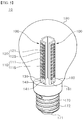
- FIG. 4 and FIG. 5 are exemplary views of an LED bulb according to a first embodiment of the present invention.
- FIG. 4 is an exemplary view of a base 170 and a holder 180 of an LED bulb 10
- FIG. 5 is an exemplary view of the LED bulb 10 with an LED package set 100 mounted thereon.
- the LED bulb 10 includes the base 170, the LED package set 100, the holder 180, and a light transmissive cover 190.
- the LED package set 100 is the LED package set 100 of FIG. 1 to FIG. 3 . See FIG. 1 to FIG. 3 for details of the LED package set 100.
- the base 170 is coupled to a socket for connection to an external power supply.
- the base 170 is formed on an outer surface thereof with a first external electrode 171 and a second external electrode 172 electrically connected to the socket.
- the first external electrode 171 and the second external electrode 172 receive electricity from the external power supply.
- the light transmissive cover 190 is coupled to the base 170 to enclose internal components such as the holder 180 and the LED package set 100.
- the light transmissive cover 190 is formed of a light transmissive material.
- the light transmissive cover 190 is formed of glass.
- the holder 180 and the LED package set 100 are disposed in the LED bulb 10.
- an interior of the LED bulb 10 is an inner space formed by coupling the base 170 to the light transmissive cover 190.
- the holder 180 is disposed under the LED package set 100 to support the LED package set 100 in an upright position.
- the holder 180 includes a connection portion 181 provided in the form of a groove or a through-hole.
- the connection portion 181 is formed therein with a pair of connection terminals 183 formed of a conductive material.
- One of the pair of connection terminals 183 is electrically connected to the first external electrode 171 of the base 170 and the other connection terminal is electrically connected to the second external electrode 172 of the base 170.
- the pair of connection terminals 183 is connected to the first external electrode 171 and the second external electrode 172 of the base 170 via conductive parts (not shown), such as wires, respectively.
- the holder 180 has been described as a separate component from the base 170. However, it should be understood that the present invention is not limited thereto and the holder 180 may be integrally formed with the base 170.
- the LED bulb 10 includes at least one LED package set 100.
- the LED bulb 10 is shown as including four LED package sets 100.
- the present invention is not limited thereto and the number of LED package sets 100 mounted on the LED bulb 10 may vary depending on choices made by those skilled in the art.
- the LED package set 100 is secured to the holder 180. One end of the LED package set 100 is inserted into the connection portion 181 of the holder 180. Thus, the LED package set 100 is disposed in an upright position inside the LED bulb 10. That is, the LED package set 100 is stood such that the first LED package 110 and the second LED package 120 face an inner surface of the light transmissive cover 190.
- the one end of the LED package set 100 inserted into the connection portion 181 corresponds to one end of the substrate 140 at which the pair of electrode pads 141 is formed.
- the pair of connection terminals 183 of the connection portion 181 is brought into contact with and electrically connected to the pair of electrode pads 141 of the substrate 140. Accordingly, electricity changed according to the dimming signal is applied to the LED package set 100 through the first external electrode 171 and the second external electrode 172 of the base 170 and the pair of connection terminals 183 of the holder 180.
- the LED bulb 10 is configured such that the LED package set 100 is secured by being inserted into the holder 180, it is easy to replace the LED package set 100 upon failure of the LED package set.
- the LED package set 100 allows light intensities of the first LED package 110 and the second LED package 120 to be regulated depending on current applied thereto. That is, color temperature of light emitted from the LED bulb 10 is changed with change in current applied from the outside.
- the LED bulb 10 can emit light having a color temperature suitable for a specific application or environment.
- the LED package set 100 includes the resistor 130 connected in series to the first LED package 110 and connected in parallel to the second LED package 120.
- current is distributed to the first LED package 110 and the second LED package 120 depending on resistance offered by the first LED package 110 and the resistor 130 and resistance offered by the second LED package 120.
- the LED bulb 10 can emit light changed in color temperature according to the dimming signal.
- the LED bulb 10 can evenly emit light laterally by including the plurality of LED package sets 100.
- FIG. 6 is an exemplary view of an LED bulb according to a second embodiment of the present invention.
- the LED bulb 20 includes at least one LED package set 200.
- the LED package set 200 is formed with a bent portion 210.
- the bent portion 210 is formed on the substrate 140 between the pair of electrode pads 141 and the first LED chip 111, the second LED chip 121, and the resistor 130.
- the bent portion 210 is formed in a transverse direction of the substrate 140.
- the transverse direction of the substrate 140 is a perpendicular direction with respect to a straight line connecting one end of the substrate 140 at which the pair of electrode pads 141 is formed to the other end of the substrate 140.
- the bent portion 210 is provided to bend the LED package set 200 at a predetermined angle.
- the bent portion 210 may be formed in any shape and by any method so long as the LED package set 200 can be bent with respect to the bent portion.
- the bent portion 210 may be formed by half-etching a portion of the substrate 140.
- the bent portion 210 may be provided in the form of at least one through-hole formed through a portion of the substrate 140.
- the bent portion 210 may be provided in the form of an indentation formed by pressing a pointed object into a portion of the substrate 140.
- the LED package set 200 may be bent about the bent portion 210 such that the first LED package 110 and the second LED package 120 face in an upward direction of the LED bulb 20, as shown in FIG. 6 .
- the LED bulb 20 including the LED package sets 200 configured as above can evenly emit light upwards as well as laterally.
- the LED bulb 20 may include an LED package set 200 bent downwards as opposed to FIG. 4 to evenly emit light laterally and downwards.
- the LED bulb 20 may include both an LED package set bent upwards and an LED package set bent downwards to evenly emit light laterally, upwards, and downwards.
Landscapes
- Engineering & Computer Science (AREA)
- Physics & Mathematics (AREA)
- Microelectronics & Electronic Packaging (AREA)
- Optics & Photonics (AREA)
- General Engineering & Computer Science (AREA)
- Led Device Packages (AREA)
- Non-Portable Lighting Devices Or Systems Thereof (AREA)
- Fastening Of Light Sources Or Lamp Holders (AREA)
Priority Applications (2)
| Application Number | Priority Date | Filing Date | Title |
|---|---|---|---|
| EP24153468.4A EP4372817A3 (fr) | 2017-05-31 | 2018-05-30 | Ampoule à del comprenant un ensemble de boîtiers de del |
| SI201831079T SI3618111T1 (sl) | 2017-05-31 | 2018-05-30 | Led sijalka s kompletom paketov svetlečih diod led |
Applications Claiming Priority (2)
| Application Number | Priority Date | Filing Date | Title |
|---|---|---|---|
| KR1020170067992A KR102400151B1 (ko) | 2017-05-31 | 2017-05-31 | 엘이디 패키지 세트 및 이를 포함하는 엘이디 벌브 |
| PCT/KR2018/006137 WO2018221952A1 (fr) | 2017-05-31 | 2018-05-30 | Ensemble de boîtiers à del et ampoule à del comprenant ce dernier |
Related Child Applications (1)
| Application Number | Title | Priority Date | Filing Date |
|---|---|---|---|
| EP24153468.4A Division EP4372817A3 (fr) | 2017-05-31 | 2018-05-30 | Ampoule à del comprenant un ensemble de boîtiers de del |
Publications (3)
| Publication Number | Publication Date |
|---|---|
| EP3618111A1 true EP3618111A1 (fr) | 2020-03-04 |
| EP3618111A4 EP3618111A4 (fr) | 2020-12-30 |
| EP3618111B1 EP3618111B1 (fr) | 2024-01-24 |
Family
ID=64456386
Family Applications (2)
| Application Number | Title | Priority Date | Filing Date |
|---|---|---|---|
| EP18809817.2A Active EP3618111B1 (fr) | 2017-05-31 | 2018-05-30 | Ampoule à del comprenant ensemble de boîtiers à del |
| EP24153468.4A Pending EP4372817A3 (fr) | 2017-05-31 | 2018-05-30 | Ampoule à del comprenant un ensemble de boîtiers de del |
Family Applications After (1)
| Application Number | Title | Priority Date | Filing Date |
|---|---|---|---|
| EP24153468.4A Pending EP4372817A3 (fr) | 2017-05-31 | 2018-05-30 | Ampoule à del comprenant un ensemble de boîtiers de del |
Country Status (6)
| Country | Link |
|---|---|
| US (3) | US11296142B2 (fr) |
| EP (2) | EP3618111B1 (fr) |
| KR (2) | KR102400151B1 (fr) |
| CN (3) | CN118315378A (fr) |
| SI (1) | SI3618111T1 (fr) |
| WO (1) | WO2018221952A1 (fr) |
Cited By (1)
| Publication number | Priority date | Publication date | Assignee | Title |
|---|---|---|---|---|
| WO2021224134A1 (fr) * | 2020-05-07 | 2021-11-11 | Signify Holding B.V. | Filament de del et lampe |
Families Citing this family (8)
| Publication number | Priority date | Publication date | Assignee | Title |
|---|---|---|---|---|
| CN111140773A (zh) * | 2018-11-06 | 2020-05-12 | 朗德万斯公司 | 用于半导体灯的多色光引擎 |
| US11209129B2 (en) * | 2019-01-29 | 2021-12-28 | Xiamen Eco Lighting Co. Ltd. | Light apparatus |
| US11212901B2 (en) * | 2019-01-29 | 2021-12-28 | Xiamen Eco Lighting Co. Ltd. | Light apparatus |
| WO2021018646A1 (fr) | 2019-07-30 | 2021-02-04 | Signify Holding B.V. | Filament de del à couleur réglable et lampe dotée d'un tel filament |
| CN111174114A (zh) * | 2020-01-15 | 2020-05-19 | 南京工业大学 | 一种新型半导体照明光源 |
| CN115479223A (zh) * | 2022-09-13 | 2022-12-16 | 东莞圣柏电子有限公司 | 一种双色灯泡 |
| KR102793157B1 (ko) * | 2022-10-28 | 2025-04-08 | 주식회사 더드림글로벌 | 용과 생장 촉진용 램프 |
| WO2026046861A1 (fr) * | 2024-08-27 | 2026-03-05 | Signify Holding B.V. | Réseau de diodes électroluminescentes comprenant des del de taille normale et des micro-del |
Family Cites Families (13)
| Publication number | Priority date | Publication date | Assignee | Title |
|---|---|---|---|---|
| US10487987B2 (en) * | 2015-08-17 | 2019-11-26 | Zhejiang Super Lighting Electric Appliance Co., Ltd. | LED filament |
| TWI354365B (en) * | 2009-08-26 | 2011-12-11 | Quasioptical led package structure for increasing | |
| KR101093952B1 (ko) * | 2010-03-08 | 2011-12-14 | 주식회사 인성전자 | 색온도 조절이 가능한 엘이디 패키지 |
| US8410726B2 (en) * | 2011-02-22 | 2013-04-02 | Quarkstar Llc | Solid state lamp using modular light emitting elements |
| KR101249673B1 (ko) * | 2011-06-28 | 2013-04-01 | 주식회사 알앤에프케미칼 | 디스플레이 화면 보호용 필름 및 상기 필름을 이용한 디스플레이 포장용 백 |
| KR101884599B1 (ko) * | 2011-08-22 | 2018-08-02 | 엘지이노텍 주식회사 | 발광 소자 패키지, 이를 포함하는 조명 장치 및 조명 시스템 |
| US9247597B2 (en) | 2011-12-02 | 2016-01-26 | Lynk Labs, Inc. | Color temperature controlled and low THD LED lighting devices and systems and methods of driving the same |
| JP2014157744A (ja) * | 2013-02-15 | 2014-08-28 | Panasonic Corp | 発光回路、発光モジュール及び照明装置 |
| JP6210830B2 (ja) * | 2013-05-27 | 2017-10-11 | シチズン時計株式会社 | Led電球 |
| TWI626395B (zh) * | 2013-06-11 | 2018-06-11 | 晶元光電股份有限公司 | 發光裝置 |
| TWI651871B (zh) * | 2013-06-27 | 2019-02-21 | 晶元光電股份有限公司 | 發光組件及製作方法 |
| CN107004751B (zh) | 2014-11-28 | 2019-05-03 | 夏普株式会社 | 发光装置以及照明器具 |
| KR20180054327A (ko) * | 2016-11-15 | 2018-05-24 | 서울반도체 주식회사 | 발광 장치 |
-
2017
- 2017-05-31 KR KR1020170067992A patent/KR102400151B1/ko active Active
-
2018
- 2018-05-30 SI SI201831079T patent/SI3618111T1/sl unknown
- 2018-05-30 CN CN202410413716.8A patent/CN118315378A/zh active Pending
- 2018-05-30 CN CN201880005640.8A patent/CN110121772B/zh active Active
- 2018-05-30 US US16/618,004 patent/US11296142B2/en active Active
- 2018-05-30 EP EP18809817.2A patent/EP3618111B1/fr active Active
- 2018-05-30 CN CN201911197367.6A patent/CN110931474A/zh active Pending
- 2018-05-30 WO PCT/KR2018/006137 patent/WO2018221952A1/fr not_active Ceased
- 2018-05-30 EP EP24153468.4A patent/EP4372817A3/fr active Pending
-
2022
- 2022-04-04 US US17/713,177 patent/US12034031B2/en active Active
- 2022-05-16 KR KR1020220059756A patent/KR102514504B1/ko active Active
-
2024
- 2024-07-08 US US18/766,483 patent/US20240363673A1/en active Pending
Cited By (1)
| Publication number | Priority date | Publication date | Assignee | Title |
|---|---|---|---|---|
| WO2021224134A1 (fr) * | 2020-05-07 | 2021-11-11 | Signify Holding B.V. | Filament de del et lampe |
Also Published As
| Publication number | Publication date |
|---|---|
| EP4372817A2 (fr) | 2024-05-22 |
| CN110121772A (zh) | 2019-08-13 |
| CN110121772B (zh) | 2024-04-26 |
| EP3618111A4 (fr) | 2020-12-30 |
| US11296142B2 (en) | 2022-04-05 |
| CN110931474A (zh) | 2020-03-27 |
| SI3618111T1 (sl) | 2024-05-31 |
| WO2018221952A1 (fr) | 2018-12-06 |
| KR20220070393A (ko) | 2022-05-31 |
| US20240363673A1 (en) | 2024-10-31 |
| KR20180131244A (ko) | 2018-12-10 |
| US12034031B2 (en) | 2024-07-09 |
| CN118315378A (zh) | 2024-07-09 |
| US20200168660A1 (en) | 2020-05-28 |
| EP3618111B1 (fr) | 2024-01-24 |
| KR102400151B1 (ko) | 2022-05-20 |
| KR102514504B1 (ko) | 2023-03-27 |
| EP4372817A3 (fr) | 2024-07-31 |
| US20220231077A1 (en) | 2022-07-21 |
Similar Documents
| Publication | Publication Date | Title |
|---|---|---|
| EP3618111B1 (fr) | Ampoule à del comprenant ensemble de boîtiers à del | |
| US12146619B2 (en) | Light bulb shaped lamp | |
| US8820950B2 (en) | Light emitting device and illumination apparatus | |
| US8911108B2 (en) | Light bulb shaped lamp and lighting apparatus | |
| EP3226313B1 (fr) | Dispositif électroluminescent et dispositif d'éclairage le comprenant | |
| US9416924B2 (en) | Light emission module | |
| WO2012086109A1 (fr) | Lampe en forme d'ampoule et dispositif d'éclairage | |
| CN102192424B (zh) | 发光装置以及照明装置 | |
| US9013097B2 (en) | Light-emitting module, lighting device, and lighting fixture | |
| KR101872253B1 (ko) | 발광 소자 패키지, 발광 장치 및 조명 장치 | |
| US20140043807A1 (en) | Device, lighting apparatus and method of assembling a light source for a lighting apparatus | |
| JP6008290B2 (ja) | 発光モジュール、照明装置および照明器具 | |
| JP2006261600A (ja) | 照明モジュール、照明装置及び照明モジュールの製造方法 | |
| US9328876B2 (en) | High efficiency LED lamp | |
| WO2014030275A1 (fr) | Lampe en forme d'ampoule et dispositif d'éclairage | |
| JP2014130728A (ja) | 照明装置 |
Legal Events
| Date | Code | Title | Description |
|---|---|---|---|
| STAA | Information on the status of an ep patent application or granted ep patent |
Free format text: STATUS: THE INTERNATIONAL PUBLICATION HAS BEEN MADE |
|
| PUAI | Public reference made under article 153(3) epc to a published international application that has entered the european phase |
Free format text: ORIGINAL CODE: 0009012 |
|
| STAA | Information on the status of an ep patent application or granted ep patent |
Free format text: STATUS: REQUEST FOR EXAMINATION WAS MADE |
|
| 17P | Request for examination filed |
Effective date: 20191128 |
|
| AK | Designated contracting states |
Kind code of ref document: A1 Designated state(s): AL AT BE BG CH CY CZ DE DK EE ES FI FR GB GR HR HU IE IS IT LI LT LU LV MC MK MT NL NO PL PT RO RS SE SI SK SM TR |
|
| AX | Request for extension of the european patent |
Extension state: BA ME |
|
| DAV | Request for validation of the european patent (deleted) | ||
| DAX | Request for extension of the european patent (deleted) | ||
| A4 | Supplementary search report drawn up and despatched |
Effective date: 20201127 |
|
| RIC1 | Information provided on ipc code assigned before grant |
Ipc: H01L 33/62 20100101ALI20201123BHEP Ipc: H01L 33/36 20100101ALI20201123BHEP Ipc: H01L 33/50 20100101ALI20201123BHEP Ipc: H01L 25/075 20060101AFI20201123BHEP Ipc: F21K 9/00 20160101ALI20201123BHEP Ipc: H01L 25/16 20060101ALI20201123BHEP |
|
| STAA | Information on the status of an ep patent application or granted ep patent |
Free format text: STATUS: EXAMINATION IS IN PROGRESS |
|
| 17Q | First examination report despatched |
Effective date: 20221121 |
|
| GRAP | Despatch of communication of intention to grant a patent |
Free format text: ORIGINAL CODE: EPIDOSNIGR1 |
|
| STAA | Information on the status of an ep patent application or granted ep patent |
Free format text: STATUS: GRANT OF PATENT IS INTENDED |
|
| INTG | Intention to grant announced |
Effective date: 20230803 |
|
| GRAS | Grant fee paid |
Free format text: ORIGINAL CODE: EPIDOSNIGR3 |
|
| GRAA | (expected) grant |
Free format text: ORIGINAL CODE: 0009210 |
|
| STAA | Information on the status of an ep patent application or granted ep patent |
Free format text: STATUS: THE PATENT HAS BEEN GRANTED |
|
| AK | Designated contracting states |
Kind code of ref document: B1 Designated state(s): AL AT BE BG CH CY CZ DE DK EE ES FI FR GB GR HR HU IE IS IT LI LT LU LV MC MK MT NL NO PL PT RO RS SE SI SK SM TR |
|
| REG | Reference to a national code |
Ref country code: GB Ref legal event code: FG4D |
|
| REG | Reference to a national code |
Ref country code: CH Ref legal event code: EP |
|
| REG | Reference to a national code |
Ref country code: IE Ref legal event code: FG4D |
|
| REG | Reference to a national code |
Ref country code: DE Ref legal event code: R096 Ref document number: 602018064555 Country of ref document: DE |
|
| REG | Reference to a national code |
Ref country code: SE Ref legal event code: TRGR |
|
| REG | Reference to a national code |
Ref country code: NL Ref legal event code: FP |
|
| REG | Reference to a national code |
Ref country code: LT Ref legal event code: MG9D |
|
| PG25 | Lapsed in a contracting state [announced via postgrant information from national office to epo] |
Ref country code: IS Free format text: LAPSE BECAUSE OF FAILURE TO SUBMIT A TRANSLATION OF THE DESCRIPTION OR TO PAY THE FEE WITHIN THE PRESCRIBED TIME-LIMIT Effective date: 20240524 |
|
| PG25 | Lapsed in a contracting state [announced via postgrant information from national office to epo] |
Ref country code: LT Free format text: LAPSE BECAUSE OF FAILURE TO SUBMIT A TRANSLATION OF THE DESCRIPTION OR TO PAY THE FEE WITHIN THE PRESCRIBED TIME-LIMIT Effective date: 20240124 |
|
| PG25 | Lapsed in a contracting state [announced via postgrant information from national office to epo] |
Ref country code: GR Free format text: LAPSE BECAUSE OF FAILURE TO SUBMIT A TRANSLATION OF THE DESCRIPTION OR TO PAY THE FEE WITHIN THE PRESCRIBED TIME-LIMIT Effective date: 20240425 |
|
| PG25 | Lapsed in a contracting state [announced via postgrant information from national office to epo] |
Ref country code: HR Free format text: LAPSE BECAUSE OF FAILURE TO SUBMIT A TRANSLATION OF THE DESCRIPTION OR TO PAY THE FEE WITHIN THE PRESCRIBED TIME-LIMIT Effective date: 20240124 Ref country code: RS Free format text: LAPSE BECAUSE OF FAILURE TO SUBMIT A TRANSLATION OF THE DESCRIPTION OR TO PAY THE FEE WITHIN THE PRESCRIBED TIME-LIMIT Effective date: 20240424 |
|
| PG25 | Lapsed in a contracting state [announced via postgrant information from national office to epo] |
Ref country code: ES Free format text: LAPSE BECAUSE OF FAILURE TO SUBMIT A TRANSLATION OF THE DESCRIPTION OR TO PAY THE FEE WITHIN THE PRESCRIBED TIME-LIMIT Effective date: 20240124 |
|
| PG25 | Lapsed in a contracting state [announced via postgrant information from national office to epo] |
Ref country code: RS Free format text: LAPSE BECAUSE OF FAILURE TO SUBMIT A TRANSLATION OF THE DESCRIPTION OR TO PAY THE FEE WITHIN THE PRESCRIBED TIME-LIMIT Effective date: 20240424 Ref country code: NO Free format text: LAPSE BECAUSE OF FAILURE TO SUBMIT A TRANSLATION OF THE DESCRIPTION OR TO PAY THE FEE WITHIN THE PRESCRIBED TIME-LIMIT Effective date: 20240424 Ref country code: LT Free format text: LAPSE BECAUSE OF FAILURE TO SUBMIT A TRANSLATION OF THE DESCRIPTION OR TO PAY THE FEE WITHIN THE PRESCRIBED TIME-LIMIT Effective date: 20240124 Ref country code: IS Free format text: LAPSE BECAUSE OF FAILURE TO SUBMIT A TRANSLATION OF THE DESCRIPTION OR TO PAY THE FEE WITHIN THE PRESCRIBED TIME-LIMIT Effective date: 20240524 Ref country code: HR Free format text: LAPSE BECAUSE OF FAILURE TO SUBMIT A TRANSLATION OF THE DESCRIPTION OR TO PAY THE FEE WITHIN THE PRESCRIBED TIME-LIMIT Effective date: 20240124 Ref country code: GR Free format text: LAPSE BECAUSE OF FAILURE TO SUBMIT A TRANSLATION OF THE DESCRIPTION OR TO PAY THE FEE WITHIN THE PRESCRIBED TIME-LIMIT Effective date: 20240425 Ref country code: FI Free format text: LAPSE BECAUSE OF FAILURE TO SUBMIT A TRANSLATION OF THE DESCRIPTION OR TO PAY THE FEE WITHIN THE PRESCRIBED TIME-LIMIT Effective date: 20240124 Ref country code: ES Free format text: LAPSE BECAUSE OF FAILURE TO SUBMIT A TRANSLATION OF THE DESCRIPTION OR TO PAY THE FEE WITHIN THE PRESCRIBED TIME-LIMIT Effective date: 20240124 Ref country code: BG Free format text: LAPSE BECAUSE OF FAILURE TO SUBMIT A TRANSLATION OF THE DESCRIPTION OR TO PAY THE FEE WITHIN THE PRESCRIBED TIME-LIMIT Effective date: 20240124 |
|
| PG25 | Lapsed in a contracting state [announced via postgrant information from national office to epo] |
Ref country code: PL Free format text: LAPSE BECAUSE OF FAILURE TO SUBMIT A TRANSLATION OF THE DESCRIPTION OR TO PAY THE FEE WITHIN THE PRESCRIBED TIME-LIMIT Effective date: 20240124 Ref country code: PT Free format text: LAPSE BECAUSE OF FAILURE TO SUBMIT A TRANSLATION OF THE DESCRIPTION OR TO PAY THE FEE WITHIN THE PRESCRIBED TIME-LIMIT Effective date: 20240524 |
|
| PG25 | Lapsed in a contracting state [announced via postgrant information from national office to epo] |
Ref country code: PT Free format text: LAPSE BECAUSE OF FAILURE TO SUBMIT A TRANSLATION OF THE DESCRIPTION OR TO PAY THE FEE WITHIN THE PRESCRIBED TIME-LIMIT Effective date: 20240524 Ref country code: PL Free format text: LAPSE BECAUSE OF FAILURE TO SUBMIT A TRANSLATION OF THE DESCRIPTION OR TO PAY THE FEE WITHIN THE PRESCRIBED TIME-LIMIT Effective date: 20240124 Ref country code: LV Free format text: LAPSE BECAUSE OF FAILURE TO SUBMIT A TRANSLATION OF THE DESCRIPTION OR TO PAY THE FEE WITHIN THE PRESCRIBED TIME-LIMIT Effective date: 20240124 |
|
| REG | Reference to a national code |
Ref country code: AT Ref legal event code: UEP Ref document number: 1652873 Country of ref document: AT Kind code of ref document: T Effective date: 20240124 |
|
| PG25 | Lapsed in a contracting state [announced via postgrant information from national office to epo] |
Ref country code: DK Free format text: LAPSE BECAUSE OF FAILURE TO SUBMIT A TRANSLATION OF THE DESCRIPTION OR TO PAY THE FEE WITHIN THE PRESCRIBED TIME-LIMIT Effective date: 20240124 |
|
| PG25 | Lapsed in a contracting state [announced via postgrant information from national office to epo] |
Ref country code: SM Free format text: LAPSE BECAUSE OF FAILURE TO SUBMIT A TRANSLATION OF THE DESCRIPTION OR TO PAY THE FEE WITHIN THE PRESCRIBED TIME-LIMIT Effective date: 20240124 |
|
| PG25 | Lapsed in a contracting state [announced via postgrant information from national office to epo] |
Ref country code: CZ Free format text: LAPSE BECAUSE OF FAILURE TO SUBMIT A TRANSLATION OF THE DESCRIPTION OR TO PAY THE FEE WITHIN THE PRESCRIBED TIME-LIMIT Effective date: 20240124 Ref country code: EE Free format text: LAPSE BECAUSE OF FAILURE TO SUBMIT A TRANSLATION OF THE DESCRIPTION OR TO PAY THE FEE WITHIN THE PRESCRIBED TIME-LIMIT Effective date: 20240124 |
|
| REG | Reference to a national code |
Ref country code: DE Ref legal event code: R097 Ref document number: 602018064555 Country of ref document: DE |
|
| PG25 | Lapsed in a contracting state [announced via postgrant information from national office to epo] |
Ref country code: SK Free format text: LAPSE BECAUSE OF FAILURE TO SUBMIT A TRANSLATION OF THE DESCRIPTION OR TO PAY THE FEE WITHIN THE PRESCRIBED TIME-LIMIT Effective date: 20240124 |
|
| PG25 | Lapsed in a contracting state [announced via postgrant information from national office to epo] |
Ref country code: SM Free format text: LAPSE BECAUSE OF FAILURE TO SUBMIT A TRANSLATION OF THE DESCRIPTION OR TO PAY THE FEE WITHIN THE PRESCRIBED TIME-LIMIT Effective date: 20240124 Ref country code: SK Free format text: LAPSE BECAUSE OF FAILURE TO SUBMIT A TRANSLATION OF THE DESCRIPTION OR TO PAY THE FEE WITHIN THE PRESCRIBED TIME-LIMIT Effective date: 20240124 Ref country code: RO Free format text: LAPSE BECAUSE OF FAILURE TO SUBMIT A TRANSLATION OF THE DESCRIPTION OR TO PAY THE FEE WITHIN THE PRESCRIBED TIME-LIMIT Effective date: 20240124 Ref country code: EE Free format text: LAPSE BECAUSE OF FAILURE TO SUBMIT A TRANSLATION OF THE DESCRIPTION OR TO PAY THE FEE WITHIN THE PRESCRIBED TIME-LIMIT Effective date: 20240124 Ref country code: DK Free format text: LAPSE BECAUSE OF FAILURE TO SUBMIT A TRANSLATION OF THE DESCRIPTION OR TO PAY THE FEE WITHIN THE PRESCRIBED TIME-LIMIT Effective date: 20240124 Ref country code: CZ Free format text: LAPSE BECAUSE OF FAILURE TO SUBMIT A TRANSLATION OF THE DESCRIPTION OR TO PAY THE FEE WITHIN THE PRESCRIBED TIME-LIMIT Effective date: 20240124 |
|
| REG | Reference to a national code |
Ref country code: DE Ref legal event code: R079 Ref document number: 602018064555 Country of ref document: DE Free format text: PREVIOUS MAIN CLASS: H01L0025075000 Ipc: H10H0029240000 |
|
| PLBE | No opposition filed within time limit |
Free format text: ORIGINAL CODE: 0009261 |
|
| STAA | Information on the status of an ep patent application or granted ep patent |
Free format text: STATUS: NO OPPOSITION FILED WITHIN TIME LIMIT |
|
| REG | Reference to a national code |
Ref country code: CH Ref legal event code: PL |
|
| 26N | No opposition filed |
Effective date: 20241025 |
|
| PG25 | Lapsed in a contracting state [announced via postgrant information from national office to epo] |
Ref country code: MC Free format text: LAPSE BECAUSE OF FAILURE TO SUBMIT A TRANSLATION OF THE DESCRIPTION OR TO PAY THE FEE WITHIN THE PRESCRIBED TIME-LIMIT Effective date: 20240124 |
|
| PG25 | Lapsed in a contracting state [announced via postgrant information from national office to epo] |
Ref country code: MC Free format text: LAPSE BECAUSE OF FAILURE TO SUBMIT A TRANSLATION OF THE DESCRIPTION OR TO PAY THE FEE WITHIN THE PRESCRIBED TIME-LIMIT Effective date: 20240124 Ref country code: CH Free format text: LAPSE BECAUSE OF NON-PAYMENT OF DUE FEES Effective date: 20240531 |
|
| PG25 | Lapsed in a contracting state [announced via postgrant information from national office to epo] |
Ref country code: IE Free format text: LAPSE BECAUSE OF NON-PAYMENT OF DUE FEES Effective date: 20240530 |
|
| PGFP | Annual fee paid to national office [announced via postgrant information from national office to epo] |
Ref country code: SI Payment date: 20250212 Year of fee payment: 8 |
|
| PGFP | Annual fee paid to national office [announced via postgrant information from national office to epo] |
Ref country code: DE Payment date: 20250220 Year of fee payment: 8 |
|
| PGFP | Annual fee paid to national office [announced via postgrant information from national office to epo] |
Ref country code: AT Payment date: 20250305 Year of fee payment: 8 |
|
| PG25 | Lapsed in a contracting state [announced via postgrant information from national office to epo] |
Ref country code: CY Free format text: LAPSE BECAUSE OF FAILURE TO SUBMIT A TRANSLATION OF THE DESCRIPTION OR TO PAY THE FEE WITHIN THE PRESCRIBED TIME-LIMIT; INVALID AB INITIO Effective date: 20180530 |
|
| PG25 | Lapsed in a contracting state [announced via postgrant information from national office to epo] |
Ref country code: HU Free format text: LAPSE BECAUSE OF FAILURE TO SUBMIT A TRANSLATION OF THE DESCRIPTION OR TO PAY THE FEE WITHIN THE PRESCRIBED TIME-LIMIT; INVALID AB INITIO Effective date: 20180530 |
|
| PGFP | Annual fee paid to national office [announced via postgrant information from national office to epo] |
Ref country code: LU Payment date: 20260220 Year of fee payment: 9 Ref country code: NL Payment date: 20260220 Year of fee payment: 9 |
|
| PGFP | Annual fee paid to national office [announced via postgrant information from national office to epo] |
Ref country code: SE Payment date: 20260223 Year of fee payment: 9 |
|
| PGFP | Annual fee paid to national office [announced via postgrant information from national office to epo] |
Ref country code: GB Payment date: 20260309 Year of fee payment: 9 |
|
| PGFP | Annual fee paid to national office [announced via postgrant information from national office to epo] |
Ref country code: BE Payment date: 20260220 Year of fee payment: 9 Ref country code: IT Payment date: 20260223 Year of fee payment: 9 |
|
| PGFP | Annual fee paid to national office [announced via postgrant information from national office to epo] |
Ref country code: FR Payment date: 20260224 Year of fee payment: 9 |
|
| PGFP | Annual fee paid to national office [announced via postgrant information from national office to epo] |
Ref country code: MT Payment date: 20260212 Year of fee payment: 9 |