EP3618253B1 - Mehrpunkt hochsetzsteller mit fliegenden kondensatoren - Google Patents
Mehrpunkt hochsetzsteller mit fliegenden kondensatoren Download PDFInfo
- Publication number
- EP3618253B1 EP3618253B1 EP19191072.8A EP19191072A EP3618253B1 EP 3618253 B1 EP3618253 B1 EP 3618253B1 EP 19191072 A EP19191072 A EP 19191072A EP 3618253 B1 EP3618253 B1 EP 3618253B1
- Authority
- EP
- European Patent Office
- Prior art keywords
- branch
- switches
- capacitor
- voltage
- vout
- Prior art date
- Legal status (The legal status is an assumption and is not a legal conclusion. Google has not performed a legal analysis and makes no representation as to the accuracy of the status listed.)
- Active
Links
Images






Classifications
-
- H—ELECTRICITY
- H02—GENERATION; CONVERSION OR DISTRIBUTION OF ELECTRIC POWER
- H02M—APPARATUS FOR CONVERSION BETWEEN AC AND AC, BETWEEN AC AND DC, OR BETWEEN DC AND DC, AND FOR USE WITH MAINS OR SIMILAR POWER SUPPLY SYSTEMS; CONVERSION OF DC OR AC INPUT POWER INTO SURGE OUTPUT POWER; CONTROL OR REGULATION THEREOF
- H02M3/00—Conversion of DC power input into DC power output
- H02M3/02—Conversion of DC power input into DC power output without intermediate conversion into AC
- H02M3/04—Conversion of DC power input into DC power output without intermediate conversion into AC by static converters
- H02M3/08—Conversion of DC power input into DC power output without intermediate conversion into AC by static converters using discharge tubes without control electrode or semiconductor devices without control electrode
-
- H—ELECTRICITY
- H02—GENERATION; CONVERSION OR DISTRIBUTION OF ELECTRIC POWER
- H02M—APPARATUS FOR CONVERSION BETWEEN AC AND AC, BETWEEN AC AND DC, OR BETWEEN DC AND DC, AND FOR USE WITH MAINS OR SIMILAR POWER SUPPLY SYSTEMS; CONVERSION OF DC OR AC INPUT POWER INTO SURGE OUTPUT POWER; CONTROL OR REGULATION THEREOF
- H02M1/00—Details of apparatus for conversion
- H02M1/36—Means for starting or stopping converters
-
- H—ELECTRICITY
- H02—GENERATION; CONVERSION OR DISTRIBUTION OF ELECTRIC POWER
- H02M—APPARATUS FOR CONVERSION BETWEEN AC AND AC, BETWEEN AC AND DC, OR BETWEEN DC AND DC, AND FOR USE WITH MAINS OR SIMILAR POWER SUPPLY SYSTEMS; CONVERSION OF DC OR AC INPUT POWER INTO SURGE OUTPUT POWER; CONTROL OR REGULATION THEREOF
- H02M1/00—Details of apparatus for conversion
- H02M1/0061—Details of apparatus for conversion using discharge tubes
-
- H—ELECTRICITY
- H02—GENERATION; CONVERSION OR DISTRIBUTION OF ELECTRIC POWER
- H02M—APPARATUS FOR CONVERSION BETWEEN AC AND AC, BETWEEN AC AND DC, OR BETWEEN DC AND DC, AND FOR USE WITH MAINS OR SIMILAR POWER SUPPLY SYSTEMS; CONVERSION OF DC OR AC INPUT POWER INTO SURGE OUTPUT POWER; CONTROL OR REGULATION THEREOF
- H02M1/00—Details of apparatus for conversion
- H02M1/32—Means for protecting converters other than automatic disconnection
-
- H—ELECTRICITY
- H02—GENERATION; CONVERSION OR DISTRIBUTION OF ELECTRIC POWER
- H02M—APPARATUS FOR CONVERSION BETWEEN AC AND AC, BETWEEN AC AND DC, OR BETWEEN DC AND DC, AND FOR USE WITH MAINS OR SIMILAR POWER SUPPLY SYSTEMS; CONVERSION OF DC OR AC INPUT POWER INTO SURGE OUTPUT POWER; CONTROL OR REGULATION THEREOF
- H02M3/00—Conversion of DC power input into DC power output
- H02M3/02—Conversion of DC power input into DC power output without intermediate conversion into AC
- H02M3/04—Conversion of DC power input into DC power output without intermediate conversion into AC by static converters
- H02M3/10—Conversion of DC power input into DC power output without intermediate conversion into AC by static converters using discharge tubes with control electrode or semiconductor devices with control electrode
- H02M3/145—Conversion of DC power input into DC power output without intermediate conversion into AC by static converters using discharge tubes with control electrode or semiconductor devices with control electrode using devices of a triode or transistor type requiring continuous application of a control signal
- H02M3/155—Conversion of DC power input into DC power output without intermediate conversion into AC by static converters using discharge tubes with control electrode or semiconductor devices with control electrode using devices of a triode or transistor type requiring continuous application of a control signal using semiconductor devices only
- H02M3/156—Conversion of DC power input into DC power output without intermediate conversion into AC by static converters using discharge tubes with control electrode or semiconductor devices with control electrode using devices of a triode or transistor type requiring continuous application of a control signal using semiconductor devices only with automatic control of output voltage or current, e.g. switching regulators
- H02M3/158—Conversion of DC power input into DC power output without intermediate conversion into AC by static converters using discharge tubes with control electrode or semiconductor devices with control electrode using devices of a triode or transistor type requiring continuous application of a control signal using semiconductor devices only with automatic control of output voltage or current, e.g. switching regulators including plural semiconductor devices as final control devices for a single load
-
- H—ELECTRICITY
- H02—GENERATION; CONVERSION OR DISTRIBUTION OF ELECTRIC POWER
- H02M—APPARATUS FOR CONVERSION BETWEEN AC AND AC, BETWEEN AC AND DC, OR BETWEEN DC AND DC, AND FOR USE WITH MAINS OR SIMILAR POWER SUPPLY SYSTEMS; CONVERSION OF DC OR AC INPUT POWER INTO SURGE OUTPUT POWER; CONTROL OR REGULATION THEREOF
- H02M7/00—Conversion of AC power input into DC power output; Conversion of DC power input into AC power output
- H02M7/42—Conversion of DC power input into AC power output without possibility of reversal
- H02M7/44—Conversion of DC power input into AC power output without possibility of reversal by static converters
- H02M7/48—Conversion of DC power input into AC power output without possibility of reversal by static converters using discharge tubes with control electrode or semiconductor devices with control electrode
- H02M7/483—Converters with outputs that each can have more than two voltages levels
- H02M7/4837—Flying capacitor converters
-
- H—ELECTRICITY
- H02—GENERATION; CONVERSION OR DISTRIBUTION OF ELECTRIC POWER
- H02M—APPARATUS FOR CONVERSION BETWEEN AC AND AC, BETWEEN AC AND DC, OR BETWEEN DC AND DC, AND FOR USE WITH MAINS OR SIMILAR POWER SUPPLY SYSTEMS; CONVERSION OF DC OR AC INPUT POWER INTO SURGE OUTPUT POWER; CONTROL OR REGULATION THEREOF
- H02M1/00—Details of apparatus for conversion
- H02M1/0003—Details of control, feedback or regulation circuits
-
- H—ELECTRICITY
- H02—GENERATION; CONVERSION OR DISTRIBUTION OF ELECTRIC POWER
- H02M—APPARATUS FOR CONVERSION BETWEEN AC AND AC, BETWEEN AC AND DC, OR BETWEEN DC AND DC, AND FOR USE WITH MAINS OR SIMILAR POWER SUPPLY SYSTEMS; CONVERSION OF DC OR AC INPUT POWER INTO SURGE OUTPUT POWER; CONTROL OR REGULATION THEREOF
- H02M3/00—Conversion of DC power input into DC power output
- H02M3/02—Conversion of DC power input into DC power output without intermediate conversion into AC
- H02M3/04—Conversion of DC power input into DC power output without intermediate conversion into AC by static converters
- H02M3/06—Conversion of DC power input into DC power output without intermediate conversion into AC by static converters using resistors or capacitors, e.g. potential divider
- H02M3/07—Conversion of DC power input into DC power output without intermediate conversion into AC by static converters using resistors or capacitors, e.g. potential divider using capacitors charged and discharged alternately by semiconductor devices with control electrode, e.g. charge pumps
Definitions
- the present disclosure relates to the field of power electronics technology, and particularly, to a multi-level boost apparatus.
- D1 ( DE102014109048A1 ) relates to a multi-level half-bridge arrangement of a voltage converter, comprising: a series connection of at least a first switching element, a second switching element, a third switching element and a fourth switching element, Low-voltage connections which are connected to an end point of the series connection of the switching elements and a center tap between the second switching element and the third switching element of the series connection, High-voltage connections, the high-voltage connections being connected to the two end points of the series connection of the switching elements, and a storage capacitor, which has a tap between the first switching element and the second switching element of the series circuit and with a further tap between the third switching element and the fourth switching element of the series circuit connected is.
- the DC/DC power conversion device includes: a DC voltage conversion section having switching elements, a charge/discharge capacitor to be charged/discharged as those elements are turned on/off, and diodes for providing charging/discharging paths; voltage dividing capacitors connected in series with each other; a first voltage equalizing diode connected forward in a direction to allow a current flow from a negative terminal of the charge/discharge capacitor to the junction of the voltage dividing capacitors 10 and 11; a first voltage equalizing Zener diode connected in an anti-series relationship thereto; a second voltage equalizing diode connected forward in a direction to allow a current flow from the junction of the voltage dividing capacitors to a positive terminal of the charge/discharge capacitor; and a second voltage equalizing Zener diode connected connected
- D3 ( EP2219275A1 ) relates to a DC/AC conversion structure, preferably intended for photovoltaic systems, having a high yield across the entire input voltage range thereof, thereby guaranteeing that direct current is not injected into the alternating current network.
- the circuit includes six switching elements controlled by a command unit.
- the circuit includes a capacitive divider having the negative of the photovoltaic field connected to one of the ends thereof and a network terminal connected at the mid-point of same, which minimises problems of electromagnetic compatibility.
- D4 JP2012239324A discloses a DC/DC power conversion apparatus including a DC voltage conversion part which is provided between a reactor connected to a DC power supply and smoothing capacitors of an output voltage and comprised of: first and second switching elements; a charge/discharge capacitor performing a charge/discharge operation depending on on-off of the first and second switching elements; and diodes forming a charge path and a discharge path of the charge/discharge capacitor.
- the DC/DC power conversion apparatus further comprises: a voltage divider resistor connected between a junction of the diodes with the smoothing capacitor and a high potential side terminal of the charge/discharge capacitor; a voltage divider resistor connected in parallel with the charge/discharge capacitor; and a voltage divider resistor connected between a low potential side terminal of the charge/discharge capacitor and a junction of the first switch element with the smoothing capacitor.
- D5 discloses a boost power conversion circuit including a first switch module, a second switch module, a first unidirectional conduction device, a second unidirectional conduction device, a flying capacitor, a third unidirectional conduction device, a third switch module, and a fourth unidirectional conduction device.
- the first switch module and the second switch module are connected in series with a power source and an inductor to form a loop.
- the first unidirectional conduction device and the second unidirectional conduction device are connected in series with a bus, an inductor, and the power source to form a loop.
- a flying capacitor and the third unidirectional conduction device are connected between a reverse stop terminal of the first unidirectional conduction device and upper and low bus capacitor midpoints; the third switch module is connected between a negative terminal of the flying capacitor and a midpoint between the first switch module and the second switch module; the fourth unidirectional conduction device is connected to two ends of a serial branch of the first unidirectional conduction device, and the second unidirectional conduction device; and the third unidirectional conduction device is used for clamping a voltage stress of the second switch module to a lower bus voltage. Therefore, a problem of over-voltage punching of the semiconductor device is solved.
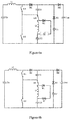
- Shown in Figure 1a is a topology of a main circuit of a conventional three-level boost apparatus of a flying-capacitor type. Under a normal condition, voltage stresses of K1, K2, D1 and D2 are all half of an output voltage Vout. Across each transistor, a withstand voltage when the circuit is started has a great difference from that when operation is in a steady state. Specifically, in a case that an input voltage Vin is higher than a withstand voltage of K2, K2 would break down and fail due to overvoltage. In a case that the input Vin is low and a difference Vout-Vin between the input and output voltages is greater than a withstand voltage of D2, D2 would break down and fail due to overvoltage. Therefore, there are great restrictive conditions for putting the solution shown in Figure 1a into practice, and advantages of the topology cannot be fully developed.
- Shown in Figure 1b is a topology of an improved main circuit of a three-level boost apparatus of a flying-capacitor type.
- the circuit is better in addressing the issue that K1 and K2 divides the voltage equally when being powered, in a case that the output voltage Vout is provided by the input voltage Vin at startup.
- a voltage on D2 is still the difference Vout-Vin between the input and output voltages, in a case that the output voltage Vout is high and the input voltage Vin is low. Therefore, D2 still has a risk of breakdown due to overvoltage.
- a multi-level boost apparatus is provided according to the present disclosure, so as to address an issue that a device has a risk of breakdown at an instant of being powered due to overvoltage in case of a low input voltage in conventional technology.
- a multi-level boost apparatus is provided, where a main circuit of the multi-level boost apparatus includes an input capacitor, an input inductor, a first branch, a second branch, a third branch, a fourth branch, and N-1 claim branches, and N is a positive integer greater that 1, and where:
- a second one of the two voltage dividing modules includes a first controllable switch and a first resistor that are connected in series, and a common node between the first one of the two dividing modules and the second one of the two dividing modules are connected via a second controllable switch to a common node between the first one of the two first switches and a second one of the two first switches.
- the i-th one of the N voltage dividing modules includes a controllable switch and a second capacitor that are connected in series for each positive integer i that is greater than 1 and smaller than or equal to N, and the second capacitor is charged in a default state of the controllable switch;
- the multi-level boost apparatus further includes N-1 connection capacitors in case of N being greater than 2, where for each positive integer j that is smaller than N-1, a terminal of a j-th one of the N-1 connection capacitors is connected to a common node between a (j+1)-th one of the N second switches and a (j+2)-th one of the N second switches, and another terminal of the j-th one of the N-1 connection capacitors is connected to a common node between a (j+1)-th one of the N voltage dividing modules and a (j+2)-th one of the N voltage dividing modules.
- the N first switches are reverse-conducting transistors
- the N second switches are diodes
- each controllable switch is a mechanical switch or a reverse-conducting transistor, where:
- each of the N-1 the clamp branches includes: a first diode and a first power source, and the first power source is configured to reduce a voltage across the i-th one of the second switches.
- the fourth branch includes N output capacitors sequentially connected in series, a first one of the N output capacitors is connected to the input capacitor, and an N-th one of the output capacitors is connected to the second branch, and each of the N-1 clamp branches includes a first diode, where:
- the i-th one of the N voltage dividing modules further includes a first impedance connected in series with the controllable switch and the second capacitor, for each positive integer i that is greater than 1 and smaller than or equal to N, where the first impedance is a resistor, an inductor or a capacitor, or is a combination of at least two of a resistor, an inductor and a capacitor.
- N is equal to 2
- the fourth branch includes two output capacitors connected in series
- a controller of the multi-level boost apparatus is configured to:
- the first impedance is the inductor
- the i-th one of the N voltage dividing module further includes a discharge branch configured to provide a discharge loop for the inductor, for each positive integer i that is greater than 1 and smaller than or equal to N.
- the discharge branch includes a second diode and a second impedance that are connected in series, and the second impedance is a resistor, a capacitor, or a combination of a resistor and a capacitor.
- the discharge branch includes a second diode and a second power source that are connected in series, and the second power source is configured to receive power from the inductor.
- the fourth branch includes multiple output capacitors sequentially connected in series, and the second power source includes all or a part of the multiple output capacitors in the fourth branch.
- N is equal to 2
- the fourth branch includes two output capacitors connected in series
- a controller of the multi-level boost apparatus is configured to:
- voltage allocation among the N first switches is achieved by arranging the N voltage dividing modules. It is prevented that the second one to the N-th one of the first switches break down and fail due to overvoltage.
- the voltage bore by the i-th second switch is clamped at a difference between the voltage across two terminals of the fourth branch (namely, the output voltage of the multi-level boost apparatus) and the voltage across the corresponding clamp branch.
- a multi-level boost apparatus is provided according to the present disclosure, so as to address an issue in conventional technology that a device has a risk of breakdown due to overvoltage at an instant of being powered under a high input voltage.
- a multi-level boost apparatus generally includes a main circuit, a voltage-and-current detection device, a controller, and the like.
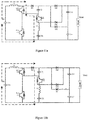
- the main circuit of the multi-level boost apparatus may be as shown in Figure 2a to Figure 2e , including: an input capacitor Cin, an input inductor L1, a first branch, a second branch, a third branch, a fourth branch and N-1 clamp branches.
- N is a positive integer greater than 1.
- a terminal of the input inductor L1 is connected to a terminal of the input capacitor Cin.
- the first branch includes N first switches (such as K11 and K12 in Figures 2a to 2d , or K11, K12 and K13 in Figure 2e ) sequentially connected in series.
- the first switch K11 connected to the input inductor L1 is the 1st first switch.
- the second branch includes N second switches (such as D01 and D02 in Figures 2a to 2d , or D01, D02 and D03 in Figure 2e ) sequentially connected in series.
- the second switch D01 connected to the input inductor L1 is the 1st second switch.
- a common node between the 1st second switch D01 and the 2nd second switch D02 is connected to a terminal of the third branch.
- the third branch includes N voltage dividing modules sequentially connected in series. The N voltage dividing modules are configured to divide a voltage across the third branch.
- a common node between an (i-1)-th voltage dividing module and an i-th voltage dividing module is connected to a common node between an (i-1)-th first switch and an i-th first switch, for each positive integer i that is greater than 1 and smaller than or equal to N.
- the 1st voltage dividing module includes a first capacitor C1.
- a common node between the (i-1)-th second switch and the i-th second switch is connected to a terminal of the (i-1)-th clamp branch.
- the (i-1)-th clamp branch is configured to reduce a voltage across the i-th second switch.
- a common node between D01 and D02 is connected to the first clamp branch (including D11 and DC11), and the 1st clamp branch is configured to reduce a voltage across the 2nd second switch D02.
- a common node between D01 and D02 is connected to the 1st clamp branch (including D11 and DC11), the 1st clamp branch is configured to reduce a voltage across the 2nd second switch D02, a common node between D02 and D03 is connected to the 2nd clamp branch (including D12 and DC12), and the 2nd clamp branch is configured to reduce a voltage across the 3rd second switch D03.
- Another terminal of the second branch is connected to a terminal of the fourth branch.
- Two terminals of the fourth branch are output terminals of the main circuit.
- a voltage across the two terminals of the fourth branch is an output voltage of the main circuit.
- the fourth branch includes at least one output capacitor (such as Cout in Figures 2a to 2e ).
- Another terminal of the first branch, another terminal of the third branch, the another terminal of the fourth branch, and another terminal of each of the N-1 clamp branches are all connected to another terminal of the input capacitor Cin.
- a 2nd voltage dividing module includes a first controllable switch K31 and a first resistor R0 that are connected in series.
- a common node between the 1st voltage dividing module and the 2nd voltage dividing module is connected via a second controllable switch K32 to a common node of the 1st first and a 2nd first switch.
- the i-th voltage dividing module includes: a controllable switch (K21 in Figure 2c and Figure 2d , or K21 and K22 in Figure 2e ) and a second capacitor (C21 in Figure 2c and Figure 2d , or C21 and C22 in Figure 2e ) that are connected in series.
- the second capacitor is charged in a default state of the controllable switch.
- positions of the controllable switch and the second capacitor are exchangeable, which are not limited to cases shown in Figures 2c to 2e , and fall within the protection scope of the present disclosure.
- the multi-level boost apparatus further includes N-1 connection capacitors (such as C3 in Figure 2e ).
- N-1 connection capacitors such as C3 in Figure 2e .
- a terminal of the j-th connection capacitor is connected to a common node between the (j+1)-th second switch and the (j+2)-th second switch, and another terminal of the j-th connection capacitor is connected to a common node between the (j+1)-th voltage dividing module and the (j+2)-th voltage dividing module, for each positive integer j that is smaller than N-1.
- the first switch may be a reverse-conducting transistor
- the second switch may be a diode.
- Each controllable switch (such as K31 and K32 in Figures 2a and 2b , K21 in Figures 2c and 2d , and K21 and K22 in Figure 2e ) may be a normally-on mechanical switch, or a reverse-conducting transistor for charging, in a default state, the second capacitor in a same voltage dividing module.
- the reverse-conducting transistor may be a MOSFET, a JFET, an IGBT integrated with an antiparallel diode, or the like, which is not specifically limited herein and fall within the protection scope of the present disclosure based on an application environment.
- the common node between the (i-1)-th second switch and the i-th second switch is a node connecting a cathode of the (i-1)-th diode and an anode of the i-th diode.
- the common node between the (i-1)-th second switch and the i-th second switch is a node connecting an anode of the (i-1)-th diode and a cathode of the i-th diode.
- Figures 2a and 2b are topologies in duality
- Figures 2c and 2d are topologies in duality
- the main circuits can achieve a three-level output.
- the dual topology for Figure 2e and the topology of a main circuit in case of N>3 can be analogized according to the above cases, which are not shown herein and fall within the protection scope of the present disclosure.
- the 2nd second switch D02 may bear a voltage difference between the output voltage and the input voltage, in the solution of the conventional technology shown in Figure 1b . Hence, a voltage stress on D02 may exceed the standard.
- the clamp branch includes a first diode (such as D11 as shown in Figure 2c ) and a first power source (such as DC11 as shown in Figure 2c).
- Figure 2c is taken as an example for illustration.
- a principle of overvoltage protection for the second switch is as follows. The clamp branch reduces the voltage on the second switch D02, and a highest voltage bore by the 2nd second switch D02 is adjusted to a difference between a voltage across the fourth branch (including Cout), namely, the output voltage of the multi-level boost apparatus, and a voltage across the clamp branch. Thereby, the voltage stress bore by the 2nd second switch D02 is reduced.
- the input inductor L1 and the second branch are both arranged on a positive cable of the multi-level boost apparatus in Figure 2c .
- a cathode of the first diode D11 is connected to a common node between corresponding two second switches (D01 and D02), an anode of the first diode D11 is connected to a positive terminal of the first power source DC11, and a negative terminal of the first power source DC11 is connected to the input capacitor Cin.
- the input inductor L1 and the second branch are both arranged on a negative cable of the multi-level boost apparatus in Figure 2d .
- the anode of the first diode D11 is connected to the common node between the corresponding two second switches (D01 and D02), the cathode of the first diode D11 is connected to the negative terminal of the first power source DC11, and the positive terminal of the first power source DC11 is connected to the input capacitor Cin.
- K22, C22, D03, D12, DC12, and C3 are added on the basis of Figure 2c . Connections among all devices refer to Figure 2e , and are not further described herein.
- principles in the topologies shown in Figures 2a , 2b , 2d and 2e and other topologies are similar to the aforementioned content, which can be analogized and are not further described herein.
- the first power source may be an additional power source. Or, a part of the output voltage of the main circuit of the multi-level boost apparatus may serve as the first power source, to reduce the voltage on the corresponding second switch.
- the fourth branch includes N output capacitors (such as Co1 and Co2 in Figures 3a to 3d , or Co1, Co2 and Co3 in Figure 3e ) connected in series.
- the output capacitor connected to the input capacitor Cin is the 1st output capacitor (such as Co1 in Figures 3a to 3e ), and the output capacitor connected to the second branch is the N-th output capacitor (such as Co2 in Figures 3a to 3d , and Co3 in Figure 3e ).
- the clamp branch includes a first diode.
- a cathode of the first diode in the (i-1)-th clamp branch is connected to the common node between the (i-1)-th second switch and the i-th second switch, and an anode of the first diode in the (i-1)-th clamp branch is connected to the common node between the (i-1)-th output capacitor and the i-th output capacitor.
- a cathode of D11 is connected to the common node between D01 and D02, and an anode of D11 is connected to the common node between Co1 and Co2.
- a cathode of D12 is connected to the common node between D02 and D03, and an anode of D12 is connected to the common node between Co2 and Co3.
- the anode of the first diode in the (i-1)-th clamp branch is connected to the common node between the (i-1)-th second switch and the i-th the second switch
- the cathode of the first diode in the (i-1)-th clamp branch is connected to the common node between the (i-1)-th output capacitor and the i-th output capacitor.
- an anode of D11 is connected to the common node between D01 and D02
- a cathode of D11 is connected to the common node between Co1 and Co2.
- Figure 3a illustrates on the basis of Figure 2a
- Figure 3b illustrates on the basis of Figure 2b
- Figure 3c illustrates on the basis of Figure 2c
- Figure 3d illustrates on the basis of Figure 2d
- Figure 3e illustrates on the basis of Figure 2e .
- Configurations of the clamp branches in other topologies can be obtained by analogy, and are not further described herein.
- a principle of overvoltage protection for the first switch in the embodiment is as follows.
- a controller controls the first controllable switch K31 to be turned off at start-up, and the first capacitor C1 can be pre-charged by the input voltage via the first controllable switch K31 and the first resistor R0.
- the controller controls the second controllable switch K32 to be turned on and the first controllable switch K31 to be turned off, so that the 1st first switch K11 is connected in parallel with the first capacitor C1.
- the voltage across the 1st first switch K11 is raised, and the voltage across the second first switch K12 is lowered.
- the voltages across the two first switches are both within a safe range, thereby preventing the second first switch K12 from breaking down due to overvoltage at start-up.
- the topology shown in Figure 2c is taken as an example for illustrate. Since parasitic capacitance of the two first switches K11 and K12 are much smaller than the first capacitor C1 and the second capacitor C21, voltage division of K11 and K12 on the input voltage at start-up can be ignored with respect to the first capacitor C1 and the second capacitor C21. Therefore, voltages bore by the two first switches K11 and K12 are determined by voltages across the first capacitor C1 and the second capacitor C21, respectively. The problem that the input voltage is completely bore by K2 in conventional technology, as shown in Figure 1 , is solved.
- the multi-level boost apparatus clamps the voltage on the i-th second switch at the difference between the voltage across the fourth branch (i.e., the output voltage of the multi-level boost apparatus) and the voltage across the corresponding clamp branch, by arranging the i-th clamp branch at a common node between the (i-1)-th second switch and the i-th second switch.
- the risk is avoided that the 2nd second switch to the N-th second switch break down due to overvoltage at an instant of being power, in a case that the input voltage is low.
- N voltage dividing modules are arranged to divide a voltage between the N first switches, and it is avoided that the 2nd first switch to the N-th first switch break down due to overvoltage.
- the embodiment adopts fewer devices to address the issue of excessive voltage stress on the switching transistor of the conventional multi-level boost circuit of a flying-capacitor type.
- Devices with lower withstand voltage can be selected for all the switching transistors, and reliable operation of the system operation guaranteed within a wide input range of the circuit. Since the circuit operates at multiple levels, a volume and a cost of relevant filter components can be well controlled, rendering the system a great advantage in cost performance.
- the voltage on the second capacitor (such as C21 in Figures 2c, 2d , 3c and 3d , and C21 and C22 in Figures 2e and 3e ) in each voltage dividing module exceeds a set limit under some special working conditions, and a sum of the voltages on the first capacitor and all the second capacitors exceeds the output voltage of the main circuit.
- the controllable switch in each voltage dividing module is turned on to discharge the corresponding second capacitor, a large current spike is introduced because the impedance of a loop is too small, and the second switches and the controllable switches in the loop are damaged.
- the i-th voltage dividing module further includes a first impedance (such as Z1 in Figure 4a ) connected in series with the controllable switch and the second capacitor.
- the first impedance is a resistor (such as R1 in Figure 4b ), an inductor (such as L2 in Figure 4c ), a capacitor (not shown), or a combination (not shown) of at least two of a resistor, an inductor and a capacitor.
- the problem of the current impulse caused by turning on the controllable switch to discharge the corresponding second capacitor can be solved by increasing the impedance of the loop.
- positions of the controllable switch, the first impedance and the second capacitor may be interchanged, which are not limited to the cases shown in Figure 4a to Figure 4c , and fall within the protection scope of the present disclosure.
- Figures 4a to 4c all illustrates on the basis of the topology shown in Figure 2c . Structures of the voltage dividing modules in other topologies may be obtained by analogy, and are not enumerated for illustration herein.
- the controller of the multi-level boost device is configured as follows.
- the second one of the two first switches in the first branch is controlled to be turned off, the first one of the two first switches is controlled to be turned on pulsingly, and the controllable switch is controlled to be turned on, to discharge the second capacitor.
- Vout is a voltage across the fourth branch.
- Vc1 is a voltage across the first capacitor.
- Vc2 is a voltage across the second capacitor.
- Vin is an input voltage of the multi-level boost apparatus.
- Vco1 is a voltage across one of the two output capacitors that is connected to the input capacitor.
- Co2 may be N times Co1, where N ⁇ 2, in other embodiments of the present disclosure.
- K11 and K12 are turned on in an interleaved manner, in a case that the main circuit enters the normal operating mode.
- the normal operating mode refers to an operating mode other than the controlling mode specified above.
- the boost device operates normally in a closed-loop manner in the normal operating mode. Waveforms of pulses for the two switches are shown in Figure 5 . T is a period of the pulses, and D is a duty cycle of the pulses.
- the i-th voltage dividing module further includes a discharge branch configured to provide a discharge loop for the inductor.
- the discharge branch includes a second diode and a second impedance that are connected in series, such as D21 and Z2 shown in Figure 6a .
- the second impedance Z2 may be a resistor (such as R2 shown in Figure 6b ), a capacitor (not shown), or a combination (not shown) of a resistor and a capacitor.
- positions of the second diode and the second impedance may be exchanged, which are not limited to the cases shown in Figure 6a and Figure 6b , and fall within the protection scope of the present disclosure.
- Figure 6a and Figure 6b both illustrates on the basis of the topology shown in Figure 4c . Structures of the discharge branches in other topologies can be obtained by analogy, and are not enumerated for illustration herein.
- the discharge branch includes a second diode and a second power source that are connected in series.
- the second power source is configured to receive power from the inductor.
- the discharge branch for the inductor L2 includes a second diode D21 and a second power source DC21.
- the second power source DC21 is capable to receive power from the inductor L2 via the second diode D21, and reuse the power.
- the second power source includes all or part of the output capacitors in the fourth branch.
- a discharge channel can be provided for the second capacitor in a case that the system is shut down, improving security of the system.
- the second diode D21 is capable to feed power from the inductor L2 back to a main bus (Cout may be an equivalent form of a capacitor or multiple capacitors). As shown in Figure 7c , the second diode D21 is capable to feed power from the inductor L2 back to a part (Co1) of the bus. Moreover, the second diode D21 is capable to provide a discharge loop for the second capacitor C21, in a case that the system is powered off.
- Figure 8a The solution shown in Figure 8a can be obtained by combining the inductor L2 and the discharge branch of L2 in Figure 7b with Figure 3c .
- Figure 8b shows a solution in which each switch transistor is replaced with a reverse-conducting switching device IGBT.
- Figure 8c is a dual topology of Figure 8a . Topologies for more levels can be obtained by analogy, and are not shown by enumeration herein.
- Figure 8b is taken as an example to illustrate an operating process and a control strategy of the controller under the several typical operating conditions as follows.
- An output load Zload is added on the basis of Figure 8b , as shown in Figure 8d .
- a specific implementation is not limited thereto, and adjustment may be made according to a practical requirement, which all fall within the protection scope of the present disclosure.
- the two first switches K11 and K12 in the first branch are controlled to be turned off.
- L2 plus C21, Co1 and Co2 are respectively charged by Vin via a current limiting resistor (not shown) and L1. Since the L2 is designed to be much smaller than L1, a voltage drop on L2 can be neglected.
- an oscillation voltage formed between L1 and C1, L2 plus C21, Co1 and Co2 is small due to existence of starting resistance and the load Zload.
- a current loop is shown in Figure 9a .
- a process for charging C1 and C21 is same as the first operating condition. Namely, firstly two first switches K11 and K12 in the first branch are both controlled to be turned off. Due to Vin ⁇ Vout, the output voltage is not charged.
- a process for charging C1 and C21 is same as that at the beginning of the second operating condition 2. Namely, firstly the two first switches K11 and K12 in the first branch are both controlled to be turned off. Since Vin is low and the voltage across C1 is not higher than the voltage across Co1, there would be a problem that Co1 directly charges C1 in a case that pulsed charging is performed as the second operating condition 2.
- Devices D11 and K12 in the loop is apt to be damaged, since impedance of the loop is extremely low in such case.
- C1 should be pre-charged under a special logic, and the start-up process of the second operating condition is not entered until the voltage across C1 is higher than the voltage across Co1.
- L1 L2 and C21 are charged by Vin, and directions of current is shown in Figure 11a .
- the directions of current is shown in Figure 11b .
- the 2nd first switch K12 in the first branch is controlled to be turned off, the 1st first switch K11 is controlled to be turned on pulsingly with a period T1, and the controllable switch K21 is controlled to be turned on pulsingly with a period T2.
- the period T2 is smaller than the period T1.
- there may be four situations as shown in Table 1, and diagrams of flowing directions of current in the situations are shown in Figures 12a, 12b , 12c and 12d .
- L2 can effectively suppress a discharge current, and power in L2 is fed back to the output terminal via D21, thereby achieving discharging without losses.
- Table 1 K11 K12 K21 Current flow diagram OFF OFF ON Figure 12a OFF OFF OFF Figure 12b ON OFF ON Figure 12c ON OFF OFF Figure 12d
- a fifth operating condition 5 is that Vin is removed at a certain moment in case of the normal operating condition of the main circuit.
- Internal energy storage devices of the system are discharged via some special discharge circuits at a bus side, to protect safety of maintenance personnel.
- C1 and C21 do not have relevant discharge loop.
- Vout is lower than the sum of the voltages across C1 and C21
- C1 is discharged by connecting to the output terminal via K12 and D02
- C21 is discharged by connecting to the output terminal through D21.
- Vout is the voltage between the two terminals of the fourth branch, namely, the output voltage of the main circuit.
- Vc1 is the voltage between the two terminals of the first capacitor.
- Vc2 is the voltage between the two terminals of the second capacitor.
- Vin is the input voltage of the multi-level boost apparatus.
- Vco1 is the voltage between the two terminals of the output capacitor that is connected to the input capacitor Cin.
- Co2 may be N times Co1, where N ⁇ 2, in other embodiments of the present disclosure.
Landscapes
- Engineering & Computer Science (AREA)
- Power Engineering (AREA)
- Dc-Dc Converters (AREA)
Claims (15)
- Mehrstufige Verstärkungsvorrichtung, wobei eine Hauptschaltung der mehrstufigen Verstärkungsvorrichtung einen Eingangskondensator (Cin), einen Eingangsinduktor (L1), einen ersten Zweig, einen zweiten Zweig, einen dritten Zweig, einen vierten Zweig und N-1 Klemmzweige umfasst;
wobei N eine positive Ganzzahl größer als 1 ist; und
wobei:ein Endgerät des Eingangsinduktors (L1) mit einem Endgerät des Eingangskondensators (Cin) verbunden ist, und ein anderes Endgerät des Eingangsinduktors (Cin) mit einem Endgerät des ersten Zweigs und ein Endgerät des zweiten Zweigs verbunden ist;der erste Zweig N erste Schalter (K11, K12, K13) umfasst, die sequentiell in Reihe geschaltet sind, wobei ein erster von den N ersten Schaltern mit dem Eingangsinduktor (L1) verbunden ist;der zweite Zweig N zweite Schalter (D01, D02, D03) umfasst, die sequentiell in Reihe geschaltet sind, wobei ein erster von den N zweiten Schaltern mit dem Eingangsinduktor (L1) verbunden ist, und ein gemeinsamer Knoten zwischen dem ersten von den N zweiten Schaltern und einem zweiten von den N zweiten Schaltern mit einem Endgerät des dritten Zweigs verbunden ist;der dritte Zweig N spannungsteilende Module umfasst, die sequentiell in Reihe geschaltet sind, wobei die N spannungsteilende Module dafür ausgelegt sind, eine Spannung quer über den dritten Zweig zu teilen, und wobei ein erstes von den N spannungsteilenden Modulen einen ersten Kondensator (C1) umfasst;für jede positive Ganzzahl i, die größer als 1 und kleiner als oder gleich N ist:ein gemeinsamer Knoten zwischen einem (i-1)-ten von den N spannungsteilenden Modulen und einem i-ten von den N spannungsteilenden Modulen mit einem gemeinsamen Knoten zwischen einem (i-1)-ten von den N ersten Schaltern und einem i-ten von den N ersten Schaltern verbunden ist; undein gemeinsamer Knoten zwischen einem (i-1)-ten von den N zweiten Schaltern und einem i-ten von den zweiten Schaltern mit einem Endgerät eines (i-1) von den N-1 Klemmzweigen verbunden ist, und der (i-1)-te von den N-1 Klemmzweigen dafür ausgelegt ist, eine Spannung auf dem i-ten von den Schaltern des zweiten Zweigs zu verringern;ein anderes Endgerät des zweiten Zweigs mit einem Endgerät des vierten Zweigs verbunden ist, wobei das Endgerät des vierten Zweigs und ein anderes Endgerät des vierten Zweigs Ausgangsendgeräte der Hauptschaltung sind, und der vierte Zweig entweder einen Ausgangkondensator (Cout) oder N Ausgangkondensatoren (Co1, Co2, Co3) umfasst, die sequentiell in Reihe geschaltet sind, wobei der erste von ihnen (Co1) mit einem anderen Endgerät des Eingangskondensators (Cin) verbunden ist; undein anderes Endgerät des ersten Zweigs, ein anderes Endgerät des dritten Zweigs, das andere Endgerät des vierten Zweigs und ein anderes Endgerät jedes der N-1 Klemmzweige mit einem anderen Endgerät des Eingangskondensators (Cin) verbunden sind, oder das andere Endgerät des oder jedes (i-1) der N-1 Klemmzweigen mit einem gemeinsamen Knoten zwischen dem (i-1)-ten und dem i-ten der N Ausgangkondensatoren (Co1, Co2, Co3, ...) verbunden ist,dadurch gekennzeichnet, dassdas i-te von den N spannungsteilenden Modulen einen steuerbaren Schalter (K21, K22) und einen zweiten Kondensator (C21, C22) umfasst, die in Reihe geschaltet sind, für jede positive Ganzzahl i, die größer als 1 und kleiner als oder gleich N ist, und der zweite Kondensator in einem Standardzustand des steuerbaren Schalters aufgeladen wird; undwobei, wenn N größer als 2 ist:die mehrstufige Verstärkungsvorrichtung weiter N-1 Verbindungskondensatoren (C3) umfasst; undfür jede positive Ganzzahl j, die kleiner als N-1 ist:ein Endgerät eines j-ten von den N-1 Verbindungskondensatoren mit einem gemeinsamen Knoten zwischen einem (j+1)-ten von den N zweiten Schaltern und einem (j+2)-ten von den N zweiten Schaltern verbunden ist; undein anderes Endgerät des j-ten von den N-1 Verbindungskondensatoren mit einem gemeinsamen Knoten zwischen einem (j+1)-ten von den N spannungsteilenden Modulen und einem (j+2)-ten von den N spannungsteilenden Modulen verbunden ist. - Mehrstufige Verstärkungsvorrichtung nach Anspruch 1, wobei die N ersten Schalter rückleitende Transistoren sind, die N zweiten Schalter Dioden sind, und jeder steuerbare Schalter ein mechanischer Schalter oder ein rückleitender Transistor ist; und
wobei:der Eingangsinduktor und der zweite Zweig auf einem positiven Kabel der mehrstufigen Verstärkungsvorrichtung angeordnet sind, und der gemeinsame Knoten zwischen einem (i-1)-ten von den N zweiten Schaltern und dem i-ten von den N zweiten Schaltern ein Knoten ist, der eine Kathode eines (i-1)-ten von den Dioden und eine Anode eines i-ten von den Dioden verbindet, für jede positive Ganzzahl i, die größer als 1 und kleiner als oder gleich N ist; oderder Eingangsinduktor und der zweite Zweig auf einem negativen Kabel der mehrstufigen Verstärkungsvorrichtung angeordnet sind, und der gemeinsame Knoten zwischen dem (i-1)-ten von den N zweiten Schaltern und dem i-ten von den N zweiten Schaltern ein Knoten ist, der zwischen einer Anode eines (i-1)-ten von den Dioden und einer Kathode eines i-ten von den Dioden verbindet, für jede positive Ganzzahl i, die größer als 1 und kleiner als oder gleich N ist. - Mehrstufige Verstärkungsvorrichtung nach Anspruch 1, wobei:
jeder der N-1 Klemmzweige eine erste Diode (D11) und eine erste Stromquelle (DC11) umfasst, und die erste Stromquelle dafür ausgelegt ist, eine Spannung quer über den i-ten von den zweiten Schaltern zu verringern. - Mehrstufige Verstärkungsvorrichtung nach Anspruch 1, wobei der vierte Zweig N Ausgangkondensatoren (Co1, Co2, Co3) umfasst, die sequentiell in Reihe geschaltet sind, wobei ein erster von den N Ausgangkondensatoren mit dem Eingangskondensator (Cin) verbunden ist, und ein N-ter von den Ausgangkondensatoren mit dem zweiten Zweig verbunden ist, und jeder von den N-1 Klemmzweigen eine erste Diode umfasst; und
wobei:der Eingangsinduktor und der zweite Zweig auf einem positiven Kabel der mehrstufigen Verstärkungsvorrichtung angeordnet sind, und eine Kathode der ersten Diode im (i-1)-ten von den N-1 Klemmzweigen mit dem gemeinsamen Knoten zwischen dem (i-1)-ten von den N zweiten Schaltern und dem i-ten von den N zweiten Schaltern verbunden ist, und eine Anode der ersten Diode im (i-1)-ten von den N-1 Klemmzweigen mit einem gemeinsamen Knoten zwischen einem (i-1)-ten von den N Ausgangkondensatoren und einem i-ten von den N Ausgangkondensatoren verbunden ist, für jede positive Ganzzahl i, die größer als 1 und kleiner als oder gleich N ist; oderder Eingangsinduktor und der zweite Zweig auf einem negativen Kabel der mehrstufigen Verstärkungsvorrichtung angeordnet sind, und eine Anode der ersten Diode im (i-1)-ten von den N-1 Klemmzweigen mit dem gemeinsamen Knoten zwischen dem (i-1)-ten von den N zweiten Schaltern und dem i-ten von den N zweiten Schaltern verbunden ist, und eine Kathode der ersten Diode im (i-1)-ten von den N-1 Klemmzweigen mit einem gemeinsamen Knoten zwischen einem (i-1)-ten von den N Ausgangkondensatoren und einem i-ten von den N Ausgangkondensatoren verbunden ist, für jede positive Ganzzahl i, die größer als 1 und kleiner als oder gleich N ist. - Mehrstufige Verstärkungsvorrichtung nach Anspruch 1, wobei:das i-te von den N spannungsteilenden Modulen weiter eine erste Impedanz (Z1) umfasst, die mit dem steuerbaren Schalter und dem zweiten Kondensator in Reihe verbunden ist, für jede positive Ganzzahl i, die größer als 1 und kleiner als oder gleich N ist, unddie erste Impedanz ein Widerstand, ein Induktor oder ein Kondensator oder eine Kombination von mindestens zwei von einem Widerstand, einem Induktor und einem Kondensator ist.
- Mehrstufige Verstärkungsvorrichtung nach Anspruch 5, wobei N gleich 2 ist, der vierte Zweig zwei Ausgangkondensatoren umfasst, die in Reihe geschaltet sind, und
wobei eine Steuereinheit der mehrstufigen Verstärkungsvorrichtung für Folgendes ausgelegt ist:Steuern der zwei ersten Schalter im ersten Zweig zum Ausschalten als Reaktion darauf, dass Vin eingeschaltet wird, und Vout=Vc1=Vc2=0, und dann Steuern der Hauptschaltung, um in einen normalen Betriebsmodus zu kommen als Reaktion auf Vout=Vin;Steuern der zwei ersten Schalter im ersten Zweig zum Ausschalten als Reaktion darauf, dass Vin eingeschaltet wird Vout/2≤Vin≤Vout und Vc1=Vc2=0; dann Steuern der zwei ersten Schalter im ersten Zweig zum pulsierenden Einschalten auf verschachtelte Art und Weise als Reaktion auf Vc1=Vc2=Vin/2, bis Vc1+Vc2=Vout; und dann Steuern der Hauptschaltung, um in den normalen Betriebsmodus zu kommen als Reaktion auf Vc1+Vc2=Vout;Steuern der zwei ersten Schalter im ersten Zweig zum Ausschalten als Reaktion darauf, dass Vin eingeschaltet wird, Vout/4≤Vin≤Vout/2 und Vc1=Vc2=0;dann Steuern eines zweiten von den zwei ersten Schaltern im ersten Zweig zum Ausschalten, und der erste von den zwei ersten Schaltern pulsierend eingeschaltet wird, als Reaktion auf Vc1=Vc2=Vin/2; dann Steuern der zwei ersten Schalter im ersten Zweig zum pulsierenden Einschalten auf verschachtelte Art und Weise als Reaktion auf Vc1 >Vco1, bis Vc1+Vc2=Vout; und dann Steuern der Hauptschaltung, um in den normalen Betriebsmodus zu kommen als Reaktion auf Vc1+Vc2=Vout; undSteuern des zweiten von den zwei ersten Schaltern im ersten Zweig zum Ausschalten, Steuern des ersten von den zwei ersten Schaltern zum pulsierenden Einschalten und Steuern des steuerbaren Schalters, um den zweiten Kondensator zu entladen, als Reaktion auf Vc1=Vout/2<Vc2 und darauf, dass die Hauptschaltung im normalen Betriebsmodus ist; undwobei Vout eine Spannung quer über den vierten Zweig ist, Vc1 eine Spannung quer über den ersten Kondensator ist, Vc2 eine Spannung quer über den zweiten Kondensator ist, Vin eine Eingangsspannung der mehrstufigen Verstärkungsvorrichtung ist, Vco1 eine Spannung quer über einen von den zwei Ausgangkondensatoren ist, der mit dem Eingangskondensator verbunden ist,wobei der erste Kondensator und der zweite Kondensator die gleiche Kapazität aufweisen, und die Kapazität des einen von den zwei Ausgangkondensatoren dreimal größer als die Kapazität eines anderen der zwei Ausgangkondensatoren ist. - Mehrstufige Verstärkungsvorrichtung nach Anspruch 5, wobei:die erste Impedanz ein Induktor ist; unddas i-te von dem N spannungsteilenden Modul weiter einen Entladungszweig umfasst, der dafür ausgelegt ist, eine Entladungsschlaufe für den Induktor bereitzustellen, für jede positive Ganzzahl i, die größer als 1 und kleiner als oder gleich N ist.
- Mehrstufige Verstärkungsvorrichtung nach Anspruch 7, wobei:der Entladungszweig eine zweite Diode (D21) und eine zweite Impedanz (Z2) umfasst, die in Reihe geschaltet sind, unddie zweite Impedanz ein Widerstand, ein Kondensator oder eine Kombination von einem Widerstand und einem Kondensator ist.
- Mehrstufige Verstärkungsvorrichtung nach Anspruch 7, wobei:der Entladungszweig eine zweite Diode (D21) und eine zweite Stromquelle (DC21) umfasst, die die in Reihe geschaltet sind, unddie zweite Stromquelle dafür ausgelegt ist, Strom vom Induktor zu empfangen.
- Mehrstufige Verstärkungsvorrichtung nach Anspruch 9, wobei:der vierte Zweig eine Mehrheit von Ausgangkondensatoren umfasst, die sequentiell in Reihe geschaltet sind; unddie zweite Stromquelle alle oder einen Teil der Mehrheit von Ausgangkondensatoren im vierten Zweig umfasst.
- Mehrstufige Verstärkungsvorrichtung nach Anspruch 10, wobei N gleich 2 ist, und der vierte Zweig zwei Ausgangkondensatoren umfasst, die in Reihe geschaltet sind;
wobei eine Steuereinheit der mehrstufigen Verstärkungsvorrichtung für Folgendes ausgelegt ist:Steuern der zwei ersten Schalter im ersten Zweig zum Ausschalten als Reaktion darauf, dass Vin eingeschaltet wird, und Vout=Vc1=Vc2=0, und dann Steuern der Hauptschaltung, um in einen normalen Betriebsmodus zu kommen als Reaktion auf Vout=Vin;Steuern der zwei ersten Schalter im ersten Zweig zum Ausschalten als Reaktion darauf, dass Vin eingeschaltet wird Vout/2≤Vin≤Vout und Vc1=Vc2=0; dann Steuern der zwei ersten Schalter im ersten Zweig zum pulsierenden Einschalten auf verschachtelte Art und Weise als Reaktion auf Vc1=Vc2=Vin/2, bis Vc1+Vc2=Vout; und dann Steuern der Hauptschaltung, um in den normalen Betriebsmodus zu kommen als Reaktion auf Vc1+Vc2=Vout;Steuern der zwei ersten Schalter im ersten Zweig zum Ausschalten als Reaktion darauf, dass Vin eingeschaltet wird, Vout/4≤Vin≤Vout/2 und Vc1=Vc2=0; dann Steuern eines zweiten von den zwei ersten Schaltern im ersten Zweig zum Ausschalten, und der erste von den zwei ersten Schaltern pulsierend eingeschaltet wird, als Reaktion auf Vc1=Vc2=Vin/2; dann Steuern der zwei ersten Schalter im ersten Zweig zum pulsierenden Einschalten auf verschachtelte Art und Weise als Reaktion auf Vc1>Vco1, bis Vc1+Vc2=Vout; und dann Steuern der Hauptschaltung, um in den normalen Betriebsmodus zu kommen als Reaktion auf Vc1+Vc2=Vout; undSteuern des zweiten von den zwei ersten Schaltern im ersten Zweig zum Ausschalten, Steuern des ersten von den zwei ersten Schaltern zum pulsierenden Einschalten mit einem Zeitraum von T1, und Steuern des steuerbaren Schalters zum pulsierenden Einschalten mit einem Zeitraum von T2, um den zweiten Kondensator zu entladen, als Reaktion auf Vc1=Vout/2<Vc2 und darauf, dass die Hauptschaltung im normalen Betriebsmodus ist, wobei T2 kleiner als T1 ist; undwobei Vout eine Spannung quer über den vierten Zweig ist, Vc1 eine Spannung quer über den ersten Kondensator ist, Vc2 eine Spannung quer über den zweiten Kondensator ist, Vin eine Eingangsspannung der mehrstufigen Verstärkungsvorrichtung ist, Vco1 eine Spannung quer über einen von den zwei Ausgangkondensatoren ist, der mit dem Eingangskondensator verbunden ist,wobei der erste Kondensator und der zweite Kondensator die gleiche Kapazität aufweisen, und die Kapazität des einen von den zwei Ausgangkondensatoren dreimal größer als die Kapazität eines anderen der zwei Ausgangkondensatoren ist. - Mehrstufige Verstärkungsvorrichtung, wobei eine Hauptschaltung der mehrstufigen Verstärkungsvorrichtung einen Eingangskondensator (Cin), einen Eingangsinduktor (L1), einen ersten Zweig, einen zweiten Zweig, einen dritten Zweig, einen vierten Zweig und einen Klemmzweig umfasst, und wobei:ein Endgerät des Eingangsinduktors (L1) mit einem Endgerät des Eingangskondensators (Cin) verbunden ist, und ein anderes Endgerät des Eingangsinduktors (L1) mit einem Endgerät des ersten Zweigs und ein Endgerät des zweiten Zweigs verbunden ist;der erste Zweig 2 erste Schalter (K11, K12) umfasst, die sequentiell in Reihe geschaltet sind, wobei ein erster von den 2 ersten Schaltern mit dem Eingangsinduktor (L1) verbunden ist;der zweite Zweig 2 zweite Schalter (D01, D02) umfasst, die sequentiell in Reihe geschaltet sind, wobei ein erster von den 2 zweiten Schaltern mit dem Eingangsinduktor (L1) verbunden ist, und ein gemeinsamer Knoten zwischen dem ersten von den 2 zweiten Schaltern und einem zweiten von den 2 zweiten Schaltern mit einem Endgerät des dritten Zweigs verbunden ist;der dritte Zweig 2 spannungsteilende Module umfasst, die sequentiell in Reihe geschaltet sind, wobei die 2 spannungsteilende Module dafür ausgelegt sind, eine Spannung quer über den dritten Zweig zu teilen, und wobei ein erstes von den 2 spannungsteilenden Modulen einen ersten Kondensator (C1) umfasst;ein gemeinsamer Knoten zwischen einem ersten von den 2 spannungsteilenden Modulen und einem zweiten von den 2 spannungsteilenden Modulen mit einem gemeinsamen Knoten zwischen einem ersten von den 2 ersten Schaltern und einem zweiten von den 2 ersten Schaltern verbunden ist; undein gemeinsamer Knoten zwischen einem ersten von den 2 zweiten Schaltern und einem zweiten von den 2 zweiten Schaltern mit einem Endgerät des Klemmzweigs verbunden ist, und der Klemmzweig dafür ausgelegt ist, eine Spannung auf dem zweiten von den Schaltern des zweiten Zweigs zu verringern;ein anderes Endgerät des zweiten Zweigs mit einem Endgerät des vierten Zweigs verbunden ist, wobei das Endgerät des vierten Zweigs und ein anderes Endgerät des vierten Zweigs Ausgangsendgeräte der Hauptschaltung sind, und der vierte Zweig entweder einen Ausgangkondensator (Cout) oder 2 Ausgangkondensatoren (Co1, Co2) umfasst, die sequentiell in Reihe geschaltet sind, wobei der erste von ihnen (Co1) mit einem anderen Endgerät des Eingangskondensators (Cin) verbunden ist; undein anderes Endgerät des ersten Zweigs, ein anderes Endgerät des dritten Zweigs, das andere Endgerät des vierten Zweigs und ein anderes Endgerät von jedem Klemmzweig mit einem anderen Endgerät des Eingangskondensators (Cin) verbunden ist oder das andere Endgerät des Klemmzweigs mit einem gemeinsamen Knoten zwischen den zwei Ausgangkondensatoren (Co1, Co2) verbunden ist,dadurch gekennzeichnet, dassein zweites von den zwei spannungsteilenden Modulen einen ersten steuerbaren Schalter (K31) und einen ersten Widerstand (R0) umfasst, die in Reihe geschaltet sind, undein gemeinsamer Knoten zwischen dem ersten von den zwei teilenden Modulen und dem zweiten von den zwei teilenden Modulen über einen zweiten steuerbaren Schalter (K32) mit einem gemeinsamen Knoten zwischen dem ersten von den zwei ersten Schaltern und einem zweiten von den zwei ersten Schaltern verbunden sind.
- Mehrstufige Verstärkungsvorrichtung nach Anspruch 12, wobei die 2 ersten Schalter rückleitende Transistoren sind, die 2 zweiten Schalter Dioden sind, und jeder steuerbare Schalter ein mechanischer Schalter oder ein rückleitender Transistor ist; und
wobei:der Eingangsinduktor und der zweite Zweig auf einem positiven Kabel der mehrstufigen Verstärkungsvorrichtung angeordnet sind, und der gemeinsame Knoten zwischen dem ersten und den 2 zweiten Schaltern und dem zweiten von den 2 zweiten Schaltern ein Knoten ist, der eine Kathode der ersten von den Dioden und eine Anode der zweiten von den Dioden verbindet;der Eingangsinduktor und der zweite Zweig auf einem negativen Kabel der mehrstufigen Verstärkungsvorrichtung angeordnet sind, und der gemeinsame Knoten zwischen dem ersten von den 2 zweiten Schaltern und dem zweiten von den zweiten Schaltern ein Knoten ist, der zwischen einer Anode der ersten von den Dioden und einer Kathode der zweiten von den Dioden verbindet. - Mehrstufige Verstärkungsvorrichtung nach Anspruch 12, wobei:
der Klemmzweig eine erste Diode und eine erste Stromquelle umfasst, und die erste Stromquelle dafür ausgelegt ist, eine Spannung quer über den zweiten von den zweiten Schaltern zu verringern. - Mehrstufige Verstärkungsvorrichtung nach Anspruch 12, wobei der vierte Zweig 2 Ausgangkondensatoren (Co1, Co2) umfasst, die sequentiell in Reihe geschaltet sind, wobei ein erster von den 2 Ausgangkondensatoren mit dem Eingangskondensator (Cin) verbunden ist, und ein zweiter von den Ausgangkondensatoren mit dem zweiten Zweig verbunden ist, und der Klemmzweig eine erste Diode umfasst; und
wobei:der Eingangsinduktor und der zweite Zweig auf einem positiven Kabel der mehrstufigen Verstärkungsvorrichtung angeordnet sind, und eine Kathode der ersten Diode im Klemmzweig mit dem gemeinsamen Knoten zwischen dem ersten von den 2 zweiten Knoten und dem zweiten von den 2 zweiten Schaltern verbunden ist, und eine Anode der ersten Diode im Klemmzweig mit einem gemeinsamen Knoten zwischen einem ersten von den 2 Ausgangkondensatoren und einem zweiten von den 2 Ausgangkondensatoren verbunden ist;der Eingangsinduktor und der zweite Zweig auf einem negativen Kabel der mehrstufigen Verstärkungsvorrichtung angeordnet sind, und eine Anode der ersten Diode im Klemmzweig mit dem gemeinsamen Knoten zwischen dem ersten von den 2 zweiten Knoten und dem zweiten von den 2 zweiten Schaltern verbunden ist, und eine Kathode der ersten Diode im Klemmzweig mit einem gemeinsamen Knoten zwischen einem ersten von den 2 Ausgangkondensatoren und einem zweiten von den zwei Ausgangkondensatoren verbunden ist.
Applications Claiming Priority (1)
| Application Number | Priority Date | Filing Date | Title |
|---|---|---|---|
| CN201810993253.1A CN109039061B (zh) | 2018-08-29 | 2018-08-29 | 一种多电平boost装置 |
Publications (2)
| Publication Number | Publication Date |
|---|---|
| EP3618253A1 EP3618253A1 (de) | 2020-03-04 |
| EP3618253B1 true EP3618253B1 (de) | 2021-06-30 |
Family
ID=64625958
Family Applications (1)
| Application Number | Title | Priority Date | Filing Date |
|---|---|---|---|
| EP19191072.8A Active EP3618253B1 (de) | 2018-08-29 | 2019-08-09 | Mehrpunkt hochsetzsteller mit fliegenden kondensatoren |
Country Status (3)
| Country | Link |
|---|---|
| US (1) | US11283354B2 (de) |
| EP (1) | EP3618253B1 (de) |
| CN (1) | CN109039061B (de) |
Cited By (1)
| Publication number | Priority date | Publication date | Assignee | Title |
|---|---|---|---|---|
| EP4597812A1 (de) * | 2024-02-05 | 2025-08-06 | Sungrow Power Supply Co., Ltd. | Dreistufiger aufwärtswandler, verfahren und vorrichtung zur steuerung eines dreistufigen aufwärtswandlers und fotovoltaisches system |
Families Citing this family (17)
| Publication number | Priority date | Publication date | Assignee | Title |
|---|---|---|---|---|
| CN108667327B (zh) * | 2018-05-03 | 2020-03-20 | 华为数字技术(苏州)有限公司 | 多电平逆变器 |
| CN109194129B (zh) * | 2018-10-26 | 2020-06-30 | 京东方科技集团股份有限公司 | 一种升压电路及其驱动方法、背光模组和显示装置 |
| CN109756115B (zh) * | 2018-12-21 | 2021-12-03 | 华为数字技术(苏州)有限公司 | 一种升压功率变换电路、方法、逆变器、装置及系统 |
| CN110165888B (zh) * | 2019-06-11 | 2024-05-14 | 阳光电源股份有限公司 | 三电平Boost电路、多路输出并联系统 |
| CN110299837A (zh) * | 2019-06-24 | 2019-10-01 | 科华恒盛股份有限公司 | 一种高压boost电路及其控制方法 |
| US11362589B2 (en) * | 2019-08-28 | 2022-06-14 | Delta Electronics, Inc. | Flying capacitor converter |
| CN110545040A (zh) * | 2019-09-11 | 2019-12-06 | 阳光电源股份有限公司 | 一种三电平Buck电路及其控制方法 |
| CN110572026A (zh) * | 2019-09-26 | 2019-12-13 | 特变电工西安电气科技有限公司 | 一种钳位型三电平升压功率变换电路 |
| CN110896278B (zh) * | 2019-12-06 | 2021-02-12 | 阳光电源股份有限公司 | 电容钳位型直流变换电路及其控制方法 |
| CN110971124A (zh) * | 2019-12-19 | 2020-04-07 | 北京理工大学 | 一种直流变换器 |
| AU2019478501B2 (en) * | 2019-12-20 | 2023-10-12 | Huawei Digital Power Technologies Co., Ltd. | Dc-dc converter |
| CN111371323B (zh) * | 2020-04-03 | 2024-06-18 | 锦浪科技股份有限公司 | 一种boost升压功率变换电路及其控制方法 |
| TWI719906B (zh) * | 2020-06-05 | 2021-02-21 | 台達電子工業股份有限公司 | 升壓電路 |
| CN113972836B (zh) * | 2020-07-22 | 2024-01-30 | 华为数字能源技术有限公司 | 一种三电平升压变换器及控制方法 |
| CN112532057B (zh) * | 2020-12-08 | 2022-02-08 | 清华大学 | 三角形多电平变换器及其控制方法 |
| CN112928907B (zh) * | 2021-02-26 | 2022-04-12 | 华中科技大学 | 一种多电平双向dc-dc变换器启动控制方法及系统 |
| US12381528B2 (en) * | 2021-03-09 | 2025-08-05 | Skyworks Solutions, Inc. | Bidirectional variable gain amplifiers for radio frequency communication systems |
Family Cites Families (19)
| Publication number | Priority date | Publication date | Assignee | Title |
|---|---|---|---|---|
| US7023186B2 (en) | 2004-08-05 | 2006-04-04 | Astec International Limited | Two stage boost converter topology |
| US7161331B2 (en) * | 2005-04-11 | 2007-01-09 | Yuan Ze University | Boost converter utilizing bi-directional magnetic energy transfer of coupling inductor |
| US7548435B2 (en) | 2006-03-31 | 2009-06-16 | Astec International Limited | Zero-voltage-switching DC-DC converters with synchronous rectifiers |
| WO2009068698A1 (es) * | 2007-11-30 | 2009-06-04 | Ingeteam Energy, S.A. | Circuito electrico para convertir energia electrica continua en energia electrica alterna |
| CN101572503A (zh) * | 2009-06-01 | 2009-11-04 | 浙江大学 | 通用型开关电容二极管箝位组合多电平电路 |
| WO2011092932A1 (ja) * | 2010-02-01 | 2011-08-04 | 三菱電機株式会社 | Dc/dc電力変換装置 |
| JP5665649B2 (ja) * | 2011-05-12 | 2015-02-04 | 三菱電機株式会社 | Dc/dc電力変換装置 |
| CN102624271B (zh) * | 2012-04-01 | 2014-07-16 | 阳光电源股份有限公司 | 一种五电平逆变拓扑单元及五电平逆变器 |
| JP2014036491A (ja) * | 2012-08-08 | 2014-02-24 | Mitsubishi Electric Corp | Dc/dc電力変換装置および太陽光発電システム用パワーコンディショナ |
| DE102014109048B4 (de) * | 2014-06-27 | 2022-02-10 | Sma Solar Technology Ag | Schaltungsanordnung mit einer Mehrfachniveau-Halbbrückenanordnung |
| CN104158208A (zh) | 2014-07-15 | 2014-11-19 | 阳光电源股份有限公司 | 一种单级光伏并网逆变器及其控制方法和应用 |
| US9979283B2 (en) * | 2014-11-05 | 2018-05-22 | Samsung Sdi Co., Ltd. | DC boosting circuit with at least one energy storage element |
| CN204302421U (zh) * | 2014-12-31 | 2015-04-29 | 武汉大学 | 一种电缆识别仪 |
| US9806601B2 (en) * | 2015-03-27 | 2017-10-31 | Futurewei Technologies, Inc. | Boost converter and method |
| CN205992854U (zh) * | 2016-07-20 | 2017-03-01 | 阳光电源股份有限公司 | 一种软启动电路和电气设备 |
| CN107070215B (zh) * | 2017-04-12 | 2023-05-16 | 特变电工西安电气科技有限公司 | 一种三电平boost共地系统及其控制方法 |
| CN108258899B (zh) * | 2017-12-29 | 2021-06-15 | 华为技术有限公司 | 一种升压功率变换电路 |
| US10554128B2 (en) * | 2018-01-05 | 2020-02-04 | Futurewei Technologies, Inc. | Multi-level boost converter |
| CN109756115B (zh) * | 2018-12-21 | 2021-12-03 | 华为数字技术(苏州)有限公司 | 一种升压功率变换电路、方法、逆变器、装置及系统 |
-
2018
- 2018-08-29 CN CN201810993253.1A patent/CN109039061B/zh active Active
-
2019
- 2019-08-09 EP EP19191072.8A patent/EP3618253B1/de active Active
- 2019-08-12 US US16/538,725 patent/US11283354B2/en active Active
Cited By (1)
| Publication number | Priority date | Publication date | Assignee | Title |
|---|---|---|---|---|
| EP4597812A1 (de) * | 2024-02-05 | 2025-08-06 | Sungrow Power Supply Co., Ltd. | Dreistufiger aufwärtswandler, verfahren und vorrichtung zur steuerung eines dreistufigen aufwärtswandlers und fotovoltaisches system |
Also Published As
| Publication number | Publication date |
|---|---|
| US11283354B2 (en) | 2022-03-22 |
| CN109039061B (zh) | 2020-03-24 |
| US20200076302A1 (en) | 2020-03-05 |
| EP3618253A1 (de) | 2020-03-04 |
| CN109039061A (zh) | 2018-12-18 |
Similar Documents
| Publication | Publication Date | Title |
|---|---|---|
| EP3618253A1 (de) | Mehrpunkt hochsetzsteller mit fliegenden kondensatoren | |
| EP3618252B1 (de) | Mehrstufige verstärkungsvorrichtung | |
| US6188209B1 (en) | Stepping inductor for fast transient response of switching converter | |
| US5710698A (en) | Delta connected resonant snubber circuit | |
| EP3174190A1 (de) | Dreipegelumrichter | |
| US6815937B2 (en) | Stepping inductor for fast transient response of switching converter | |
| US5642273A (en) | Resonant snubber inverter | |
| US20040140792A1 (en) | Control IC for low power auxiliary supplies | |
| WO2020248583A1 (zh) | 三电平Boost电路、多路输出并联系统 | |
| CN105680793B (zh) | 一种光伏系统的电压补偿装置及光伏系统 | |
| EP4423912B1 (de) | Gate-unit für einen gate-kommutierten thyristor und integrierter gate-kommutierter thyristor | |
| CN105453405A (zh) | 多电平变换器 | |
| US20200007030A1 (en) | Electrical Circuit for Zero-Voltage Soft-Switching in DC-DC Converter Under All Load Conditions | |
| Hu et al. | A single-switch trans-inverse high step-up semiquadratic DC–DC converter based on three-winding coupled inductor | |
| Guo et al. | An expandable interline DC power flow controller | |
| EP4589830A1 (de) | Gleichstromwandlerschaltung und photovoltaikwechselrichter | |
| Huang et al. | Single-phase dual-mode four-switch Buck-Boost Transformerless PV inverter with inherent leakage current elimination | |
| CN111342693A (zh) | 一种升降压型光伏并网逆变器 | |
| Chakraborty et al. | Design concept of a high power high frequency power supply for feeding 500 kV, 100 mA Cockcroft-Walton generator | |
| US20200321874A1 (en) | Power conversion apparatus, and power supply apparatus | |
| Ting et al. | A modular DC-DC converter with collapsible input voltage of series connected modules without additional bypass switch | |
| Elserougi et al. | A bi-directional boost converter-based non-isolated DC-DC transformer with modular solid-state switches for medium-/high-voltage DC grids | |
| Eitzen et al. | Modular dc-dc converter system for energy harvesting with eaps | |
| Kumle et al. | Z-source online UPS | |
| Radika | A high efficiency DC-DC Boost converter with passive regenerative snubber |
Legal Events
| Date | Code | Title | Description |
|---|---|---|---|
| PUAI | Public reference made under article 153(3) epc to a published international application that has entered the european phase |
Free format text: ORIGINAL CODE: 0009012 |
|
| STAA | Information on the status of an ep patent application or granted ep patent |
Free format text: STATUS: THE APPLICATION HAS BEEN PUBLISHED |
|
| AK | Designated contracting states |
Kind code of ref document: A1 Designated state(s): AL AT BE BG CH CY CZ DE DK EE ES FI FR GB GR HR HU IE IS IT LI LT LU LV MC MK MT NL NO PL PT RO RS SE SI SK SM TR |
|
| AX | Request for extension of the european patent |
Extension state: BA ME |
|
| STAA | Information on the status of an ep patent application or granted ep patent |
Free format text: STATUS: REQUEST FOR EXAMINATION WAS MADE |
|
| 17P | Request for examination filed |
Effective date: 20200331 |
|
| RBV | Designated contracting states (corrected) |
Designated state(s): AL AT BE BG CH CY CZ DE DK EE ES FI FR GB GR HR HU IE IS IT LI LT LU LV MC MK MT NL NO PL PT RO RS SE SI SK SM TR |
|
| GRAP | Despatch of communication of intention to grant a patent |
Free format text: ORIGINAL CODE: EPIDOSNIGR1 |
|
| STAA | Information on the status of an ep patent application or granted ep patent |
Free format text: STATUS: GRANT OF PATENT IS INTENDED |
|
| RIC1 | Information provided on ipc code assigned before grant |
Ipc: H02M 1/36 20070101ALI20210114BHEP Ipc: H02M 3/158 20060101AFI20210114BHEP Ipc: H02M 3/07 20060101ALN20210114BHEP Ipc: H02M 1/32 20070101ALI20210114BHEP |
|
| INTG | Intention to grant announced |
Effective date: 20210129 |
|
| GRAS | Grant fee paid |
Free format text: ORIGINAL CODE: EPIDOSNIGR3 |
|
| GRAA | (expected) grant |
Free format text: ORIGINAL CODE: 0009210 |
|
| STAA | Information on the status of an ep patent application or granted ep patent |
Free format text: STATUS: THE PATENT HAS BEEN GRANTED |
|
| AK | Designated contracting states |
Kind code of ref document: B1 Designated state(s): AL AT BE BG CH CY CZ DE DK EE ES FI FR GB GR HR HU IE IS IT LI LT LU LV MC MK MT NL NO PL PT RO RS SE SI SK SM TR |
|
| REG | Reference to a national code |
Ref country code: CH Ref legal event code: EP |
|
| REG | Reference to a national code |
Ref country code: DE Ref legal event code: R096 Ref document number: 602019005709 Country of ref document: DE Ref country code: AT Ref legal event code: REF Ref document number: 1407286 Country of ref document: AT Kind code of ref document: T Effective date: 20210715 |
|
| REG | Reference to a national code |
Ref country code: IE Ref legal event code: FG4D |
|
| REG | Reference to a national code |
Ref country code: LT Ref legal event code: MG9D |
|
| PG25 | Lapsed in a contracting state [announced via postgrant information from national office to epo] |
Ref country code: BG Free format text: LAPSE BECAUSE OF FAILURE TO SUBMIT A TRANSLATION OF THE DESCRIPTION OR TO PAY THE FEE WITHIN THE PRESCRIBED TIME-LIMIT Effective date: 20210930 Ref country code: HR Free format text: LAPSE BECAUSE OF FAILURE TO SUBMIT A TRANSLATION OF THE DESCRIPTION OR TO PAY THE FEE WITHIN THE PRESCRIBED TIME-LIMIT Effective date: 20210630 Ref country code: FI Free format text: LAPSE BECAUSE OF FAILURE TO SUBMIT A TRANSLATION OF THE DESCRIPTION OR TO PAY THE FEE WITHIN THE PRESCRIBED TIME-LIMIT Effective date: 20210630 |
|
| REG | Reference to a national code |
Ref country code: NL Ref legal event code: MP Effective date: 20210630 |
|
| REG | Reference to a national code |
Ref country code: AT Ref legal event code: MK05 Ref document number: 1407286 Country of ref document: AT Kind code of ref document: T Effective date: 20210630 |
|
| PG25 | Lapsed in a contracting state [announced via postgrant information from national office to epo] |
Ref country code: GR Free format text: LAPSE BECAUSE OF FAILURE TO SUBMIT A TRANSLATION OF THE DESCRIPTION OR TO PAY THE FEE WITHIN THE PRESCRIBED TIME-LIMIT Effective date: 20211001 Ref country code: RS Free format text: LAPSE BECAUSE OF FAILURE TO SUBMIT A TRANSLATION OF THE DESCRIPTION OR TO PAY THE FEE WITHIN THE PRESCRIBED TIME-LIMIT Effective date: 20210630 Ref country code: SE Free format text: LAPSE BECAUSE OF FAILURE TO SUBMIT A TRANSLATION OF THE DESCRIPTION OR TO PAY THE FEE WITHIN THE PRESCRIBED TIME-LIMIT Effective date: 20210630 Ref country code: LV Free format text: LAPSE BECAUSE OF FAILURE TO SUBMIT A TRANSLATION OF THE DESCRIPTION OR TO PAY THE FEE WITHIN THE PRESCRIBED TIME-LIMIT Effective date: 20210630 Ref country code: NO Free format text: LAPSE BECAUSE OF FAILURE TO SUBMIT A TRANSLATION OF THE DESCRIPTION OR TO PAY THE FEE WITHIN THE PRESCRIBED TIME-LIMIT Effective date: 20210930 |
|
| PG25 | Lapsed in a contracting state [announced via postgrant information from national office to epo] |
Ref country code: CZ Free format text: LAPSE BECAUSE OF FAILURE TO SUBMIT A TRANSLATION OF THE DESCRIPTION OR TO PAY THE FEE WITHIN THE PRESCRIBED TIME-LIMIT Effective date: 20210630 Ref country code: AT Free format text: LAPSE BECAUSE OF FAILURE TO SUBMIT A TRANSLATION OF THE DESCRIPTION OR TO PAY THE FEE WITHIN THE PRESCRIBED TIME-LIMIT Effective date: 20210630 Ref country code: NL Free format text: LAPSE BECAUSE OF FAILURE TO SUBMIT A TRANSLATION OF THE DESCRIPTION OR TO PAY THE FEE WITHIN THE PRESCRIBED TIME-LIMIT Effective date: 20210630 Ref country code: RO Free format text: LAPSE BECAUSE OF FAILURE TO SUBMIT A TRANSLATION OF THE DESCRIPTION OR TO PAY THE FEE WITHIN THE PRESCRIBED TIME-LIMIT Effective date: 20210630 Ref country code: PT Free format text: LAPSE BECAUSE OF FAILURE TO SUBMIT A TRANSLATION OF THE DESCRIPTION OR TO PAY THE FEE WITHIN THE PRESCRIBED TIME-LIMIT Effective date: 20211102 Ref country code: SM Free format text: LAPSE BECAUSE OF FAILURE TO SUBMIT A TRANSLATION OF THE DESCRIPTION OR TO PAY THE FEE WITHIN THE PRESCRIBED TIME-LIMIT Effective date: 20210630 Ref country code: SK Free format text: LAPSE BECAUSE OF FAILURE TO SUBMIT A TRANSLATION OF THE DESCRIPTION OR TO PAY THE FEE WITHIN THE PRESCRIBED TIME-LIMIT Effective date: 20210630 Ref country code: ES Free format text: LAPSE BECAUSE OF FAILURE TO SUBMIT A TRANSLATION OF THE DESCRIPTION OR TO PAY THE FEE WITHIN THE PRESCRIBED TIME-LIMIT Effective date: 20210630 Ref country code: EE Free format text: LAPSE BECAUSE OF FAILURE TO SUBMIT A TRANSLATION OF THE DESCRIPTION OR TO PAY THE FEE WITHIN THE PRESCRIBED TIME-LIMIT Effective date: 20210630 |
|
| PG25 | Lapsed in a contracting state [announced via postgrant information from national office to epo] |
Ref country code: PL Free format text: LAPSE BECAUSE OF FAILURE TO SUBMIT A TRANSLATION OF THE DESCRIPTION OR TO PAY THE FEE WITHIN THE PRESCRIBED TIME-LIMIT Effective date: 20210630 |
|
| REG | Reference to a national code |
Ref country code: DE Ref legal event code: R097 Ref document number: 602019005709 Country of ref document: DE |
|
| PG25 | Lapsed in a contracting state [announced via postgrant information from national office to epo] |
Ref country code: MC Free format text: LAPSE BECAUSE OF FAILURE TO SUBMIT A TRANSLATION OF THE DESCRIPTION OR TO PAY THE FEE WITHIN THE PRESCRIBED TIME-LIMIT Effective date: 20210630 |
|
| REG | Reference to a national code |
Ref country code: BE Ref legal event code: MM Effective date: 20210831 |
|
| PG25 | Lapsed in a contracting state [announced via postgrant information from national office to epo] |
Ref country code: DK Free format text: LAPSE BECAUSE OF FAILURE TO SUBMIT A TRANSLATION OF THE DESCRIPTION OR TO PAY THE FEE WITHIN THE PRESCRIBED TIME-LIMIT Effective date: 20210630 |
|
| PLBE | No opposition filed within time limit |
Free format text: ORIGINAL CODE: 0009261 |
|
| STAA | Information on the status of an ep patent application or granted ep patent |
Free format text: STATUS: NO OPPOSITION FILED WITHIN TIME LIMIT |
|
| REG | Reference to a national code |
Ref country code: DE Ref legal event code: R082 Ref document number: 602019005709 Country of ref document: DE Representative=s name: ZACCO LEGAL RECHTSANWALTSGESELLSCHAFT MBH, DE |
|
| PG25 | Lapsed in a contracting state [announced via postgrant information from national office to epo] |
Ref country code: LU Free format text: LAPSE BECAUSE OF NON-PAYMENT OF DUE FEES Effective date: 20210809 Ref country code: AL Free format text: LAPSE BECAUSE OF FAILURE TO SUBMIT A TRANSLATION OF THE DESCRIPTION OR TO PAY THE FEE WITHIN THE PRESCRIBED TIME-LIMIT Effective date: 20210630 |
|
| 26N | No opposition filed |
Effective date: 20220331 |
|
| PG25 | Lapsed in a contracting state [announced via postgrant information from national office to epo] |
Ref country code: IT Free format text: LAPSE BECAUSE OF FAILURE TO SUBMIT A TRANSLATION OF THE DESCRIPTION OR TO PAY THE FEE WITHIN THE PRESCRIBED TIME-LIMIT Effective date: 20210630 Ref country code: IE Free format text: LAPSE BECAUSE OF NON-PAYMENT OF DUE FEES Effective date: 20210809 Ref country code: BE Free format text: LAPSE BECAUSE OF NON-PAYMENT OF DUE FEES Effective date: 20210831 |
|
| REG | Reference to a national code |
Ref country code: CH Ref legal event code: PL |
|
| PG25 | Lapsed in a contracting state [announced via postgrant information from national office to epo] |
Ref country code: LT Free format text: LAPSE BECAUSE OF FAILURE TO SUBMIT A TRANSLATION OF THE DESCRIPTION OR TO PAY THE FEE WITHIN THE PRESCRIBED TIME-LIMIT Effective date: 20210630 Ref country code: LI Free format text: LAPSE BECAUSE OF NON-PAYMENT OF DUE FEES Effective date: 20220831 Ref country code: CH Free format text: LAPSE BECAUSE OF NON-PAYMENT OF DUE FEES Effective date: 20220831 |
|
| P01 | Opt-out of the competence of the unified patent court (upc) registered |
Effective date: 20230426 |
|
| PG25 | Lapsed in a contracting state [announced via postgrant information from national office to epo] |
Ref country code: CY Free format text: LAPSE BECAUSE OF FAILURE TO SUBMIT A TRANSLATION OF THE DESCRIPTION OR TO PAY THE FEE WITHIN THE PRESCRIBED TIME-LIMIT Effective date: 20210630 |
|
| PG25 | Lapsed in a contracting state [announced via postgrant information from national office to epo] |
Ref country code: HU Free format text: LAPSE BECAUSE OF FAILURE TO SUBMIT A TRANSLATION OF THE DESCRIPTION OR TO PAY THE FEE WITHIN THE PRESCRIBED TIME-LIMIT; INVALID AB INITIO Effective date: 20190809 |
|
| PG25 | Lapsed in a contracting state [announced via postgrant information from national office to epo] |
Ref country code: MK Free format text: LAPSE BECAUSE OF FAILURE TO SUBMIT A TRANSLATION OF THE DESCRIPTION OR TO PAY THE FEE WITHIN THE PRESCRIBED TIME-LIMIT Effective date: 20210630 |
|
| PG25 | Lapsed in a contracting state [announced via postgrant information from national office to epo] |
Ref country code: TR Free format text: LAPSE BECAUSE OF FAILURE TO SUBMIT A TRANSLATION OF THE DESCRIPTION OR TO PAY THE FEE WITHIN THE PRESCRIBED TIME-LIMIT Effective date: 20210630 |
|
| PG25 | Lapsed in a contracting state [announced via postgrant information from national office to epo] |
Ref country code: MT Free format text: LAPSE BECAUSE OF FAILURE TO SUBMIT A TRANSLATION OF THE DESCRIPTION OR TO PAY THE FEE WITHIN THE PRESCRIBED TIME-LIMIT Effective date: 20210630 |
|
| REG | Reference to a national code |
Ref country code: DE Ref legal event code: R082 Ref document number: 602019005709 Country of ref document: DE |
|
| PGFP | Annual fee paid to national office [announced via postgrant information from national office to epo] |
Ref country code: DE Payment date: 20250916 Year of fee payment: 7 |
|
| PGFP | Annual fee paid to national office [announced via postgrant information from national office to epo] |
Ref country code: GB Payment date: 20250919 Year of fee payment: 7 |
|
| PGFP | Annual fee paid to national office [announced via postgrant information from national office to epo] |
Ref country code: FR Payment date: 20250829 Year of fee payment: 7 |