EP3618585A1 - Support de circuit doté d'un emplacement de montage pour composants électroniques, circuits électroniques et procédé de fabrication - Google Patents
Support de circuit doté d'un emplacement de montage pour composants électroniques, circuits électroniques et procédé de fabrication Download PDFInfo
- Publication number
- EP3618585A1 EP3618585A1 EP18192045.5A EP18192045A EP3618585A1 EP 3618585 A1 EP3618585 A1 EP 3618585A1 EP 18192045 A EP18192045 A EP 18192045A EP 3618585 A1 EP3618585 A1 EP 3618585A1
- Authority
- EP
- European Patent Office
- Prior art keywords
- circuit carrier
- depot
- edge
- recess
- formation
- Prior art date
- Legal status (The legal status is an assumption and is not a legal conclusion. Google has not performed a legal analysis and makes no representation as to the accuracy of the status listed.)
- Withdrawn
Links
Images



Classifications
-
- H—ELECTRICITY
- H05—ELECTRIC TECHNIQUES NOT OTHERWISE PROVIDED FOR
- H05K—PRINTED CIRCUITS; CASINGS OR CONSTRUCTIONAL DETAILS OF ELECTRIC APPARATUS; MANUFACTURE OF ASSEMBLAGES OF ELECTRICAL COMPONENTS
- H05K3/00—Apparatus or processes for manufacturing printed circuits
- H05K3/22—Secondary treatment of printed circuits
- H05K3/28—Applying non-metallic protective coatings
- H05K3/284—Applying non-metallic protective coatings for encapsulating mounted components
-
- H—ELECTRICITY
- H10—SEMICONDUCTOR DEVICES; ELECTRIC SOLID-STATE DEVICES NOT OTHERWISE PROVIDED FOR
- H10W—GENERIC PACKAGES, INTERCONNECTIONS, CONNECTORS OR OTHER CONSTRUCTIONAL DETAILS OF DEVICES COVERED BY CLASS H10
- H10W72/00—Interconnections or connectors in packages
- H10W72/30—Die-attach connectors
-
- H—ELECTRICITY
- H10—SEMICONDUCTOR DEVICES; ELECTRIC SOLID-STATE DEVICES NOT OTHERWISE PROVIDED FOR
- H10W—GENERIC PACKAGES, INTERCONNECTIONS, CONNECTORS OR OTHER CONSTRUCTIONAL DETAILS OF DEVICES COVERED BY CLASS H10
- H10W74/00—Encapsulations, e.g. protective coatings
- H10W74/01—Manufacture or treatment
- H10W74/012—Manufacture or treatment of encapsulations on active surfaces of flip-chip devices, e.g. forming underfills
-
- H—ELECTRICITY
- H10—SEMICONDUCTOR DEVICES; ELECTRIC SOLID-STATE DEVICES NOT OTHERWISE PROVIDED FOR
- H10W—GENERIC PACKAGES, INTERCONNECTIONS, CONNECTORS OR OTHER CONSTRUCTIONAL DETAILS OF DEVICES COVERED BY CLASS H10
- H10W74/00—Encapsulations, e.g. protective coatings
- H10W74/10—Encapsulations, e.g. protective coatings characterised by their shape or disposition
- H10W74/15—Encapsulations, e.g. protective coatings characterised by their shape or disposition on active surfaces of flip-chip devices, e.g. underfills
-
- H—ELECTRICITY
- H05—ELECTRIC TECHNIQUES NOT OTHERWISE PROVIDED FOR
- H05K—PRINTED CIRCUITS; CASINGS OR CONSTRUCTIONAL DETAILS OF ELECTRIC APPARATUS; MANUFACTURE OF ASSEMBLAGES OF ELECTRICAL COMPONENTS
- H05K1/00—Printed circuits
- H05K1/02—Details
- H05K1/0201—Thermal arrangements, e.g. for cooling, heating or preventing overheating
- H05K1/0203—Cooling of mounted components
- H05K1/0204—Cooling of mounted components using means for thermal conduction connection in the thickness direction of the substrate
-
- H—ELECTRICITY
- H05—ELECTRIC TECHNIQUES NOT OTHERWISE PROVIDED FOR
- H05K—PRINTED CIRCUITS; CASINGS OR CONSTRUCTIONAL DETAILS OF ELECTRIC APPARATUS; MANUFACTURE OF ASSEMBLAGES OF ELECTRICAL COMPONENTS
- H05K2201/00—Indexing scheme relating to printed circuits covered by H05K1/00
- H05K2201/09—Shape and layout
- H05K2201/09009—Substrate related
- H05K2201/09036—Recesses or grooves in insulating substrate
-
- H—ELECTRICITY
- H05—ELECTRIC TECHNIQUES NOT OTHERWISE PROVIDED FOR
- H05K—PRINTED CIRCUITS; CASINGS OR CONSTRUCTIONAL DETAILS OF ELECTRIC APPARATUS; MANUFACTURE OF ASSEMBLAGES OF ELECTRICAL COMPONENTS
- H05K2201/00—Indexing scheme relating to printed circuits covered by H05K1/00
- H05K2201/09—Shape and layout
- H05K2201/09209—Shape and layout details of conductors
- H05K2201/09654—Shape and layout details of conductors covering at least two types of conductors provided for in H05K2201/09218 - H05K2201/095
- H05K2201/09745—Recess in conductor, e.g. in pad or in metallic substrate
-
- H—ELECTRICITY
- H05—ELECTRIC TECHNIQUES NOT OTHERWISE PROVIDED FOR
- H05K—PRINTED CIRCUITS; CASINGS OR CONSTRUCTIONAL DETAILS OF ELECTRIC APPARATUS; MANUFACTURE OF ASSEMBLAGES OF ELECTRICAL COMPONENTS
- H05K2201/00—Indexing scheme relating to printed circuits covered by H05K1/00
- H05K2201/10—Details of components or other objects attached to or integrated in a printed circuit board
- H05K2201/10613—Details of electrical connections of non-printed components, e.g. special leads
- H05K2201/10954—Other details of electrical connections
- H05K2201/10977—Encapsulated connections
-
- H—ELECTRICITY
- H05—ELECTRIC TECHNIQUES NOT OTHERWISE PROVIDED FOR
- H05K—PRINTED CIRCUITS; CASINGS OR CONSTRUCTIONAL DETAILS OF ELECTRIC APPARATUS; MANUFACTURE OF ASSEMBLAGES OF ELECTRICAL COMPONENTS
- H05K2203/00—Indexing scheme relating to apparatus or processes for manufacturing printed circuits covered by H05K3/00
- H05K2203/01—Tools for processing; Objects used during processing
- H05K2203/0186—Mask formed or laid on PCB, the mask having recesses or openings specially designed for mounting components or body parts thereof
-
- H—ELECTRICITY
- H05—ELECTRIC TECHNIQUES NOT OTHERWISE PROVIDED FOR
- H05K—PRINTED CIRCUITS; CASINGS OR CONSTRUCTIONAL DETAILS OF ELECTRIC APPARATUS; MANUFACTURE OF ASSEMBLAGES OF ELECTRICAL COMPONENTS
- H05K2203/00—Indexing scheme relating to apparatus or processes for manufacturing printed circuits covered by H05K3/00
- H05K2203/04—Soldering or other types of metallurgic bonding
- H05K2203/0415—Small preforms other than balls, e.g. discs, cylinders or pillars
-
- H—ELECTRICITY
- H05—ELECTRIC TECHNIQUES NOT OTHERWISE PROVIDED FOR
- H05K—PRINTED CIRCUITS; CASINGS OR CONSTRUCTIONAL DETAILS OF ELECTRIC APPARATUS; MANUFACTURE OF ASSEMBLAGES OF ELECTRICAL COMPONENTS
- H05K2203/00—Indexing scheme relating to apparatus or processes for manufacturing printed circuits covered by H05K3/00
- H05K2203/11—Treatments characterised by their effect, e.g. heating, cooling, roughening
- H05K2203/1178—Means for venting or for letting gases escape
-
- H—ELECTRICITY
- H05—ELECTRIC TECHNIQUES NOT OTHERWISE PROVIDED FOR
- H05K—PRINTED CIRCUITS; CASINGS OR CONSTRUCTIONAL DETAILS OF ELECTRIC APPARATUS; MANUFACTURE OF ASSEMBLAGES OF ELECTRICAL COMPONENTS
- H05K3/00—Apparatus or processes for manufacturing printed circuits
- H05K3/0011—Working of insulating substrates or insulating layers
- H05K3/0044—Mechanical working of the substrate, e.g. drilling or punching
-
- H—ELECTRICITY
- H05—ELECTRIC TECHNIQUES NOT OTHERWISE PROVIDED FOR
- H05K—PRINTED CIRCUITS; CASINGS OR CONSTRUCTIONAL DETAILS OF ELECTRIC APPARATUS; MANUFACTURE OF ASSEMBLAGES OF ELECTRICAL COMPONENTS
- H05K3/00—Apparatus or processes for manufacturing printed circuits
- H05K3/30—Assembling printed circuits with electric components, e.g. with resistors
- H05K3/303—Assembling printed circuits with electric components, e.g. with resistors with surface mounted components
- H05K3/305—Affixing by adhesive
-
- H—ELECTRICITY
- H05—ELECTRIC TECHNIQUES NOT OTHERWISE PROVIDED FOR
- H05K—PRINTED CIRCUITS; CASINGS OR CONSTRUCTIONAL DETAILS OF ELECTRIC APPARATUS; MANUFACTURE OF ASSEMBLAGES OF ELECTRICAL COMPONENTS
- H05K3/00—Apparatus or processes for manufacturing printed circuits
- H05K3/30—Assembling printed circuits with electric components, e.g. with resistors
- H05K3/32—Assembling printed circuits with electric components, e.g. with resistors electrically connecting electric components or wires to printed circuits
- H05K3/34—Assembling printed circuits with electric components, e.g. with resistors electrically connecting electric components or wires to printed circuits by soldering
- H05K3/341—Surface mounted components
-
- H—ELECTRICITY
- H05—ELECTRIC TECHNIQUES NOT OTHERWISE PROVIDED FOR
- H05K—PRINTED CIRCUITS; CASINGS OR CONSTRUCTIONAL DETAILS OF ELECTRIC APPARATUS; MANUFACTURE OF ASSEMBLAGES OF ELECTRICAL COMPONENTS
- H05K3/00—Apparatus or processes for manufacturing printed circuits
- H05K3/30—Assembling printed circuits with electric components, e.g. with resistors
- H05K3/32—Assembling printed circuits with electric components, e.g. with resistors electrically connecting electric components or wires to printed circuits
- H05K3/34—Assembling printed circuits with electric components, e.g. with resistors electrically connecting electric components or wires to printed circuits by soldering
- H05K3/341—Surface mounted components
- H05K3/3431—Leadless components
-
- H—ELECTRICITY
- H10—SEMICONDUCTOR DEVICES; ELECTRIC SOLID-STATE DEVICES NOT OTHERWISE PROVIDED FOR
- H10W—GENERIC PACKAGES, INTERCONNECTIONS, CONNECTORS OR OTHER CONSTRUCTIONAL DETAILS OF DEVICES COVERED BY CLASS H10
- H10W72/00—Interconnections or connectors in packages
- H10W72/071—Connecting or disconnecting
- H10W72/073—Connecting or disconnecting of die-attach connectors
- H10W72/07331—Connecting techniques
-
- H—ELECTRICITY
- H10—SEMICONDUCTOR DEVICES; ELECTRIC SOLID-STATE DEVICES NOT OTHERWISE PROVIDED FOR
- H10W—GENERIC PACKAGES, INTERCONNECTIONS, CONNECTORS OR OTHER CONSTRUCTIONAL DETAILS OF DEVICES COVERED BY CLASS H10
- H10W72/00—Interconnections or connectors in packages
- H10W72/071—Connecting or disconnecting
- H10W72/073—Connecting or disconnecting of die-attach connectors
- H10W72/07351—Connecting or disconnecting of die-attach connectors characterised by changes in properties of the die-attach connectors during connecting
- H10W72/07354—Connecting or disconnecting of die-attach connectors characterised by changes in properties of the die-attach connectors during connecting changes in dispositions
-
- H—ELECTRICITY
- H10—SEMICONDUCTOR DEVICES; ELECTRIC SOLID-STATE DEVICES NOT OTHERWISE PROVIDED FOR
- H10W—GENERIC PACKAGES, INTERCONNECTIONS, CONNECTORS OR OTHER CONSTRUCTIONAL DETAILS OF DEVICES COVERED BY CLASS H10
- H10W72/00—Interconnections or connectors in packages
- H10W72/30—Die-attach connectors
- H10W72/341—Dispositions of die-attach connectors, e.g. layouts
- H10W72/347—Dispositions of multiple die-attach connectors
-
- H—ELECTRICITY
- H10—SEMICONDUCTOR DEVICES; ELECTRIC SOLID-STATE DEVICES NOT OTHERWISE PROVIDED FOR
- H10W—GENERIC PACKAGES, INTERCONNECTIONS, CONNECTORS OR OTHER CONSTRUCTIONAL DETAILS OF DEVICES COVERED BY CLASS H10
- H10W72/00—Interconnections or connectors in packages
- H10W72/90—Bond pads, in general
- H10W72/921—Structures or relative sizes of bond pads
- H10W72/926—Multiple bond pads having different sizes
Definitions
- the invention relates to a circuit carrier with a slot for an electronic component.
- the invention relates to an electronic circuit with such a circuit carrier.
- the invention also relates to a method for producing a circuit carrier, in which an installation space for an electronic component is generated.
- the invention also relates to a method for producing an electronic assembly in which such a circuit carrier is used.
- Circuit carriers and electronic circuits are widely used in today's products.
- power electronics circuits which are used, for example, in rectifiers and converters.
- Good thermal and electrical contacting of power semiconductors in such power electronic circuits must be ensured so that their function is unrestricted.
- the good thermal and electrical properties with a low overall height must be guaranteed by the contact structure. If the overall height is reduced, however, the use of an insulation medium, preferably around the outside of the power component, is also required.
- underfill material underfill material
- the insulation material which is also referred to as underfill material (underfill material)
- underfill material must ensure that outgassing from the Joint zone can penetrate to the outside and do not form bubbles in the underfill material.
- outgassing frequently leads to bubbles during backfilling.
- the following underfill materials are used as backfill materials: epoxy resins optimized for underflows with and without fillers.
- the object of the invention is therefore to provide a circuit carrier with a slot for electronic components or an electronic circuit with such a circuit carrier, in which the possibility of a bubble-free filling with an underfill material is improved.
- circuit carrier circuit carrier in that a formation is provided at the edge of the depot.
- the introduction of a formation which is designed as a depression, has the advantage when filling the gap between the component and the circuit carrier that the formation remains free of underfill material longer than the remaining gap between the component and the circuit carrier. This makes it possible for outgassing to escape from the joining gap (hereinafter also referred to as gap) during the filling process while the underfill material is spreading in the gap.
- the underfill material forms a flow front. The shape is arranged at the edge of the installation location in such a way that the flow front can run towards it in the gap. This means that the formation is only closed by the underfill material so that the recess can transport the outgassing to the outside until the very end. The formation of bubbles is therefore advantageously avoided.
- the edge of the installation space is defined by the outer edge of the component to be installed. In other words, when designing the installation space on the circuit carrier, it must be taken into account which dimensions the component has to be assembled.
- the formation is then to be provided in the circuit carrier in the region of the imaginary outer edge of the component. For example, this can be done in such a way that part of the formation on the edge of the installation space points outwards. This creates a kind of "guardrail" for the outgassing and underfill material, while the latter is distributed in the gap.
- the gap should be chosen as narrow as possible.
- a sintered material is used as the contacting material, very narrow gaps can advantageously be realized. With conventional contact deposits made of sintered material, these can be, for example, in a range from 20 micrometers to 100 micrometers.
- the installation locations are usually essentially rectangular or square, preferably also U-shaped. It is particularly advantageous if the recesses are arranged at the edge of the old construction site in such a way that they are located in the middle between the corners of the installation site. An underfilling of the gap can then take place particularly advantageously starting from the corners, so that the flow fronts move from the corners of the installation location to the formation and finally reach the formation.
- the formation advantageously represents an obstacle to flow, since the underfill material has to overcome resistance in order to flow around the edge of the formation.
- the formation advantageously keeps a path which is necessary for outgassing open for a relatively long time and which only closes when the flow fronts of the underfill material on the formation from opposite directions to meet. The result is a bubble-free or at least largely bubble-free underfill result.
- the depot consists of a sintered material, it is possible to provide formations which have a comparatively fine geometry. This is due to the fact that the sintered deposits essentially retain their shape during joining (apart from shrinkage), so that these fine structures are retained. This is different with solder materials that are melted to produce the connection. Here, fine formations would be lost due to the surface tension of the liquid solder material.
- the formations advantageously support the discharge of outgassing during the filling of the gap with underfill material.
- the formations have the task of guiding the underfill material in a certain direction when it arrives at the form with its flow front, so that, for example, it can be prevented from penetrating into areas in which bubbles can be enclosed.
- the formations can advantageously also be used in such a way that the flow front is directed towards a flow obstacle such as a recess in the form of a depression (more on this in the following).
- the recesses which provide an edge of the depression as a flow obstacle, then cause the flow front to be stopped until the recess also fills with underfill material at the end. Until then, the recess can be used as a channel for transporting outgassing.
- the formations can be prevented by diverting the flow fronts or by stopping the flow fronts, the underfill material, which fills the gap from different corners of an installation location, flows together too early and would thus prevent outgassing with the consequence of bubbles.
- the formations can, if one assumes square or rectangular installation spaces, be arranged in the middle between two corners.
- a formation in the sense of the invention is to be understood as a structure which protrudes from the edge of the deposit made of sintered material and thus forms an obstacle which stops or deflects an underfill material flowing along the deposit.
- the shape has the shape of a wedge that protrudes from the edge of the depot.
- a wedge-shaped shape is arranged so that the wedge lies on its triangular surface, so to speak.
- the wedge-shaped configuration as a prism with a triangular base area, this prism adjoining the depot with one of its side faces.
- the width of the wedge corresponds exactly to the height of the depot.
- the wedge fills the gap as far as possible over its entire gap height.
- the gap width is given by the height of the solder deposit, this is only the case if the width of the wedge corresponds to the height of the deposit.
- the redirecting function of the formation is advantageously used most effectively.
- a mask is used which has a mask opening containing the shape, the filling of this Mask opening next to the deposit made of sintered material at the same time creates the formation at the same height.
- a depot of a joining aid in particular of a sintered material, is applied to the installation location.
- the shape can also have different geometries than that of a wedge.
- This can also be cuboidal, for example, the cuboid adjoining the side of the deposit made of sintering paste, so to speak. It is also advantageous here if the cuboid has the same height as the depot.
- the formation has the shape of a half cylinder, which connects with its flat side surface to the deposit made of sintered paste. It is also advantageous here if the height of this half cylinder corresponds to the height of the depot.
- the joining aid that is to say the sintered material
- the circuit carrier is usually already provided with joining aid for assembly purposes. This can be printed out of sintering paste, for example. If printing errors occur during this process, this can be determined optically before the components are installed, so that this error can be rejected or corrected at an early stage.
- preforms can also be used, which can advantageously be manufactured particularly precisely. These are fixed in the installation location or placed directly before the component is installed.
- the mounting space has at least one recess on its edge, which forms a recess in the surface of the circuit carrier.
- Surface structuring is understood to mean an adaptation of the surface such that this is used as a flow obstacle for the underfill material. This can be achieved, for example, by roughening the surface with a laser, for example.
- the advantages of the invention are explained below with reference to the recesses. Of course, these apply analogously but also when using the surface structuring.
- a recess which is designed as a depression
- the additional introduction of a recess has the advantage when filling the gap between the component and the circuit carrier that the recess remains free of underfill material longer than the remaining gap between the component and the circuit carrier.
- the underfill material forms a flow front.
- the recess is arranged at the edge of the installation location in such a way that the flow front can run towards it in the gap. This means that the recess is only closed by the underfill material so that the recess can transport the outgassing to the outside until the very end. The formation of bubbles is therefore advantageously avoided.
- the edge of the installation space is defined by the outer edge of the component to be installed. In other words, when designing the installation space on the circuit carrier, it must be taken into account which dimensions the component has to be assembled.
- the recess is then to be provided in the circuit carrier in the region of the imaginary outer edge of the component. For example, this can be done in such a way that part of the recess lies within the installation space and part of the recess lies outside the installation space. This creates a kind of channel or "tunnel" for the outgassing while the underfill material is distributed in the gap.
- the recess consists of a slot which runs perpendicular to the edge of the installation location.
- a slot which runs perpendicular to the edge of the installation space, can lie on both sides of the edge of the installation space and therefore fulfills this task particularly well.
- such a slot can advantageously be easily produced, for example, by micromilling or laser processing.
- the recess is provided in an insulation layer forming the surface of the circuit carrier, in particular consisting of a solder resist, and / or in a metallization on the circuit carrier.
- the depression for example the slot
- all layers of the layer structure of the circuit carrier are available for its formation.
- the insulation layer is normally brought up to the installation location and ends at a certain distance from the installation location so that it can be reliably kept free of insulation material. If this layer consists of a solder resist, for example, this is usually developed photochemically.
- the recesses can be taken into account right from the start and can be formed in situ with the production using the solder stop layer.
- the metallization is also applied as a layer on the circuit carrier and is structured to form contact areas and conductor tracks. In this structuring process (for example by etching technology), the recess can be advantageous be made in situ during processing.
- the recesses can be formed both in the insulation layer and in the metallization, for example by micromilling or laser processing. These methods have the advantage of very high accuracy, so that the recesses can be made precisely. In particular, the sharp edges of the depression required to stop the flow front of the underfill material can be excellently formed by this method.
- the object is also achieved according to the invention with the initially stated subject matter (electronic circuit) in that the circuit carrier is designed in accordance with the invention, the electronic component being fastened to the depot of the joining aid.
- the electronic circuit is an implementation in which the circuit carrier is used for the end product, which has already been explained in detail above. If such an electronic assembly is underfilled with underfill material, bubble-free underfill results can be achieved, which achieves the above object.
- the bubble-free underfill material advantageously improves both the heat conduction and the electrical insulation in the electronic assembly.
- a gap between the circuit carrier and the component is filled with an underfill material.
- the object is also achieved according to the invention with the claim object (mask) specified at the outset in that the at least one opening has indentations at the edge, depots with projections being printable with the indentations.
- the object is also achieved according to the invention with the initially stated subject matter (method) in that a molding is provided at the edge of the depot.
- the product produced namely the circuit carrier, can advantageously be used to produce the electronic assembly explained above.
- the advantages associated with this have already been mentioned and should not be mentioned again here.
- the formation is produced in the form of a wedge which projects from the edge of the depot.
- the wedge-shaped design of the formation has the advantage that this structure has a favorable geometry for redirecting underfill material.
- the structures can also have a different geometry, as has already been explained above.
- the wedge is produced with a width that corresponds precisely to the height of the depot.
- At least one recess is created at the edge of the installation space, this recess being formed as a depression in the surface of the circuit carrier.
- the recess is produced by a machining process, in particular by milling or drilling.
- cutting processes such as micromilling or drilling allow particularly high accuracies.
- the required edges which form the edge of the depression, can be formed with sharp edges in the recesses.
- Elongated recesses can be created during milling. Depending on whether the axis of rotation of the milling head is perpendicular or parallel to the surface of the circuit carrier, the elongated recesses can have a sharp edge all around or have a tapering edge at their ends. The tapered edge at the end of the recesses can be used as a flow aid so that the recess is still filled with underfill material at the end of the underfilling process.
- recess is produced by structuring a layer, in particular by structuring an insulation layer on the circuit carrier.
- the underfill material is introduced into the gap in an area outside the at least one shape, preferably exactly in the middle between two shapes.
- the underfill material advantageously expands evenly on both sides when it is introduced in the middle between two formations. If this is not the case, the formations serve as a flow obstacle to eliminate these irregularities. Reliable outgassing is therefore easily possible. If, as already explained, a square or rectangular installation space is provided and the protrusions are provided in the middle of the side edges, the middle between the protrusions is usually at the corners (in the case of square installation spaces or near the corners (in the case of rectangular installation spaces).
- the described components of the embodiments each represent individual features of the invention that are to be considered independently of one another, which also further develop the invention independently of one another and are therefore also to be regarded individually or in a combination other than the one shown as part of the invention. Furthermore, the described embodiments can also be supplemented by further features of the invention that have already been described.
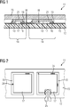
- An electronic circuit 11 which has a circuit carrier 12 and electronic components 13.
- the electronic components 13 are each provided in slots 14 of the circuit carrier 12.
- the installation locations 14 result from openings being formed in an insulation layer 15 from a solder resist.
- a depot 16 is provided in each of these openings on the surface of the circuit carrier 12 (compare, for example Figure 3 ) a sintered connection 17 was remelted.
- a remaining gap 18 is filled with an underfill material 19, which closes the gap between the component 13 and the circuit carrier 12.
- the electronic circuit 11 has a cover plate 20 which is connected to the respective upper sides of the components 13 via a further sintered connection 21.
- Figure 1 is the electronic circuit 11 without any recesses 22 or formations 23 (but compare Figures 3 to 7 ).
- the shapes and recesses shown in these figures can, however, lie in front of or behind the cutting plane that in FIG Figure 1 is shown. In this respect, the variants according to the figures mentioned can be integrated into the electronic circuit 11 according to Figure 1 be introduced.
- Figure 1 shows a structure of how this would look according to the prior art without any recesses and shapes.
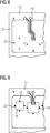
- a structure was produced for test purposes, this structure being in the sectional plane II - II (see Figure 1 ) was cut open. In this sectional plane, a grinding surface can be seen, which is formed by the sintered connection 17.
- This sintered connection 17 is surrounded by the underfill material 19. Since the electronic circuit 11 according to Figure 2 was produced without recesses and formations, when casting the gap 18 (see Figure 1 ) Bubbles 24 formed in the underfill material, which have their origin from outgassing of the sintered connection 17. This formation of bubbles must be prevented with the formations and recesses according to the invention.
- Figure 3 is a section of the electronic assembly shown, according to Figure 1 can be built.
- the cutout represents an edge of the recess 14 in which the component 13 can also be seen.
- the edge of the recess 14 is formed by the insulation layer 15 below the component 13.
- the insulation layer 15 does not reach the depot 16 made of a sintered material which is applied to a contact layer which is part of a structured metallization 26.
- the metallization 26 and the insulation layer 15 are each on the surface 27 of the circuit carrier 12.
- the formation 23 can also be seen, which is connected to the depot 26 and can for example be wedge-shaped, in the form of a half-cylinder or cuboid. Like that Figures 5 to 7 can be seen, this formation 23 connects in the middle of the depot 16 to the outside and stands out from it (hence the term formation).
- the sintered deposits 16 have the advantage that this shape is retained even after the heat treatment for the purpose of joining the sintered connection, since the sintered bodies which form the deposits 16 remain dimensionally stable during the joining.
- the respective geometry of the formations can also be found. These have the height of the depot 16 and are each connected to the outer edges.
- the formation consists of a wedge.
- this is a triangular prism, which adjoins the outside of the depot 16 with one of its three side surfaces and thus projects from the side edge with the opposite tip. The base and the top surface of this prism are thus on the level of the bottom and the top of the depot 16, respectively.
- the formation 23 is designed as a half cylinder, which projects outwards with the part of the round outer surface and lies with the straight cut surface on the side surface of the depot 16. Base and top surface are thus again in one level with the top and bottom of the depot 16.
- the formation 23 is cube-shaped, one of the side surfaces of this cube lying on the side surface of the depot 16.
- the upper and the lower side of the cube each form a common surface with the top and the bottom of the depot 16.
- the circuit carrier 12 can be seen with a metallization, which in addition to the contact structures 25 also has the recesses 22.
- the recesses required for this can be produced, for example, by etching in the metallization.
- a print mask that has a negative form of the in Figure 3 forms illustrated metal structures. In other words, such a mask has etching openings wherever according to Figure 8 the surface 27 of the circuit carrier 12 comes to light.
- Figure 9 is shown as on the circuit carrier 12 according to Figure 8 the depots 16 were applied from sinter paste. It can also be seen here that the formations 23 with correspond to the recesses 22, so that the to Figure 4 described effect of redirecting the underfill material can be achieved. It can also be seen that the depots 16 made of sintering paste for some components consist of several segments in order to different contacts of the electronic component to be joined (in Figure 9 to ensure).
- FIG. 10 A printing stencil is shown which has mask openings 28 at the locations which the depots 16 according to Figure 9 should be printed. It can be seen that the formations 23 according to FIG Figure 9 are realized by indentations 29 in the mask openings 28. These are filled with the material, for example the sintering paste, during printing so that the depots 16 show the formations 23.
Landscapes
- Engineering & Computer Science (AREA)
- Manufacturing & Machinery (AREA)
- Microelectronics & Electronic Packaging (AREA)
- Wire Bonding (AREA)
Priority Applications (1)
| Application Number | Priority Date | Filing Date | Title |
|---|---|---|---|
| EP18192045.5A EP3618585A1 (fr) | 2018-08-31 | 2018-08-31 | Support de circuit doté d'un emplacement de montage pour composants électroniques, circuits électroniques et procédé de fabrication |
Applications Claiming Priority (1)
| Application Number | Priority Date | Filing Date | Title |
|---|---|---|---|
| EP18192045.5A EP3618585A1 (fr) | 2018-08-31 | 2018-08-31 | Support de circuit doté d'un emplacement de montage pour composants électroniques, circuits électroniques et procédé de fabrication |
Publications (1)
| Publication Number | Publication Date |
|---|---|
| EP3618585A1 true EP3618585A1 (fr) | 2020-03-04 |
Family
ID=63490231
Family Applications (1)
| Application Number | Title | Priority Date | Filing Date |
|---|---|---|---|
| EP18192045.5A Withdrawn EP3618585A1 (fr) | 2018-08-31 | 2018-08-31 | Support de circuit doté d'un emplacement de montage pour composants électroniques, circuits électroniques et procédé de fabrication |
Country Status (1)
| Country | Link |
|---|---|
| EP (1) | EP3618585A1 (fr) |
Cited By (1)
| Publication number | Priority date | Publication date | Assignee | Title |
|---|---|---|---|---|
| EP4340005A1 (fr) * | 2022-09-19 | 2024-03-20 | Siemens Aktiengesellschaft | Module électronique sous-rempli avec structures de guidage de la direction du débit |
Citations (3)
| Publication number | Priority date | Publication date | Assignee | Title |
|---|---|---|---|---|
| US6094354A (en) * | 1996-12-03 | 2000-07-25 | Nec Corporation | Chip component mounting board, chip component mounting structure, and method of manufacturing chip component mounting board |
| DE102010063021A1 (de) * | 2010-12-14 | 2012-06-14 | Robert Bosch Gmbh | Elektronische Baugruppe mit verbesserter Sinterverbindung |
| DE102016111871A1 (de) * | 2015-06-29 | 2017-03-16 | Infineon Technologies Austria Ag | Stromverteilung in Gleichspannungswandlern |
-
2018
- 2018-08-31 EP EP18192045.5A patent/EP3618585A1/fr not_active Withdrawn
Patent Citations (3)
| Publication number | Priority date | Publication date | Assignee | Title |
|---|---|---|---|---|
| US6094354A (en) * | 1996-12-03 | 2000-07-25 | Nec Corporation | Chip component mounting board, chip component mounting structure, and method of manufacturing chip component mounting board |
| DE102010063021A1 (de) * | 2010-12-14 | 2012-06-14 | Robert Bosch Gmbh | Elektronische Baugruppe mit verbesserter Sinterverbindung |
| DE102016111871A1 (de) * | 2015-06-29 | 2017-03-16 | Infineon Technologies Austria Ag | Stromverteilung in Gleichspannungswandlern |
Cited By (1)
| Publication number | Priority date | Publication date | Assignee | Title |
|---|---|---|---|---|
| EP4340005A1 (fr) * | 2022-09-19 | 2024-03-20 | Siemens Aktiengesellschaft | Module électronique sous-rempli avec structures de guidage de la direction du débit |
Similar Documents
| Publication | Publication Date | Title |
|---|---|---|
| DE10221891C5 (de) | Leistungshalbleitervorrichtung | |
| EP3036761B1 (fr) | Procédé de soudage par diffusion d'un composant électronique avec une surface de montage avec des enfoncements sur un substrat | |
| DE2108792C3 (fr) | ||
| DE69534483T2 (de) | Leiterrahmen und Halbleiterbauelement | |
| DE2049093B2 (de) | Relaistraeger- und anschlussplatte fuer eine schaltanordnung | |
| EP2962799B1 (fr) | Module semi-conducteur doté de raccords soudés aux ultrasons | |
| DE10335622A1 (de) | Harzversiegelte Halbleiterbaugruppe | |
| DE10316096B4 (de) | Platte mit gedruckter Schaltung und mit einer barrieregeschützten Durchgangsöffnung und Verfahren zu deren Herstellung | |
| AT520301B1 (de) | Verfahren zum erzeugen einer leiterplatte mit thermischen durchkontaktierungen, sowie leiterplatte | |
| EP3618586A1 (fr) | Support de circuit doté d'un emplacement de montage pour composants électroniques, circuits électroniques et procédé de fabrication | |
| EP3291654B1 (fr) | Module de commande pour un véhicule automobile | |
| EP3618585A1 (fr) | Support de circuit doté d'un emplacement de montage pour composants électroniques, circuits électroniques et procédé de fabrication | |
| DE102021120935B4 (de) | Verfahren zum Formen eines Halbleiter-Leistungsmoduls | |
| DE102016109227A1 (de) | Verfahren und Vorrichtung zum simultanen Verkapseln von Halbleiter-Dies mit geschichteten Leadframe-Streifen | |
| DE112015003364T5 (de) | Schaltungsanordnung | |
| DE102004016940B4 (de) | Schaltungsträger für einen Halbleiterchip und ein Bauelement mit einem Halbleiterchip | |
| DE1259123B (de) | Elektrische Programmiertafel sowie Verfahren zu ihrer Herstellung | |
| EP4320549A1 (fr) | Corps de puce destiné à une carte à puce, carte à puce et procédé de production d'un corps de puce | |
| DE19921867C2 (de) | Verfahren zur Herstellung eines Halbleiterbauelements mit mindestens einem verkapselten Chip auf einem Substrat | |
| EP1170793B1 (fr) | Matrice porteuse avec une zone de connexion pour un circuit intégré et procédé pour sa fabrication | |
| EP0184608A2 (fr) | Procédé pour la fabrication de connecteurs multiples mécaniquement séparables pour le raccordement électrique de composants micro-électroniques et connecteurs multiples fabriqués suivant ce procédé | |
| WO2024068546A1 (fr) | Dispositif électrique et son procédé de formation | |
| EP4697865A1 (fr) | Carte de circuit imprimé avec au moins un composant soudé | |
| DE2156292A1 (de) | Verbindungsstelle von stromfuehrenden bauteilen | |
| DE102024127418A1 (de) | Halbleitermodul |
Legal Events
| Date | Code | Title | Description |
|---|---|---|---|
| PUAI | Public reference made under article 153(3) epc to a published international application that has entered the european phase |
Free format text: ORIGINAL CODE: 0009012 |
|
| AK | Designated contracting states |
Kind code of ref document: A1 Designated state(s): AL AT BE BG CH CY CZ DE DK EE ES FI FR GB GR HR HU IE IS IT LI LT LU LV MC MK MT NL NO PL PT RO RS SE SI SK SM TR |
|
| AX | Request for extension of the european patent |
Extension state: BA ME |
|
| STAA | Information on the status of an ep patent application or granted ep patent |
Free format text: STATUS: THE APPLICATION IS DEEMED TO BE WITHDRAWN |
|
| 18D | Application deemed to be withdrawn |
Effective date: 20200905 |