EP3621047B1 - System und verfahren zum erkennen von manipulationen an einem produkt - Google Patents
System und verfahren zum erkennen von manipulationen an einem produkt Download PDFInfo
- Publication number
- EP3621047B1 EP3621047B1 EP18192899.5A EP18192899A EP3621047B1 EP 3621047 B1 EP3621047 B1 EP 3621047B1 EP 18192899 A EP18192899 A EP 18192899A EP 3621047 B1 EP3621047 B1 EP 3621047B1
- Authority
- EP
- European Patent Office
- Prior art keywords
- capacitor
- slope
- integrated circuit
- capacitance
- segments
- Prior art date
- Legal status (The legal status is an assumption and is not a legal conclusion. Google has not performed a legal analysis and makes no representation as to the accuracy of the status listed.)
- Active
Links
Images



Classifications
-
- G—PHYSICS
- G08—SIGNALLING
- G08B—SIGNALLING SYSTEMS, e.g. PERSONAL CALLING SYSTEMS; ORDER TELEGRAPHS; ALARM SYSTEMS
- G08B13/00—Burglar, theft or intruder alarms
- G08B13/22—Electrical actuation
- G08B13/24—Electrical actuation by interference with electromagnetic field distribution
- G08B13/2402—Electronic Article Surveillance [EAS], i.e. systems using tags for detecting removal of a tagged item from a secure area, e.g. tags for detecting shoplifting
- G08B13/2428—Tag details
- G08B13/2448—Tag with at least dual detection means, e.g. combined inductive and ferromagnetic tags, dual frequencies within a single technology, tampering detection or signalling means on the tag
-
- G—PHYSICS
- G06—COMPUTING OR CALCULATING; COUNTING
- G06K—GRAPHICAL DATA READING; PRESENTATION OF DATA; RECORD CARRIERS; HANDLING RECORD CARRIERS
- G06K19/00—Record carriers for use with machines and with at least a part designed to carry digital markings
- G06K19/06—Record carriers for use with machines and with at least a part designed to carry digital markings characterised by the kind of the digital marking, e.g. shape, nature, code
- G06K19/067—Record carriers with conductive marks, printed circuits or semiconductor circuit elements, e.g. credit or identity cards also with resonating or responding marks without active components
- G06K19/07—Record carriers with conductive marks, printed circuits or semiconductor circuit elements, e.g. credit or identity cards also with resonating or responding marks without active components with integrated circuit chips
- G06K19/073—Special arrangements for circuits, e.g. for protecting identification code in memory
- G06K19/07309—Means for preventing undesired reading or writing from or onto record carriers
- G06K19/07372—Means for preventing undesired reading or writing from or onto record carriers by detecting tampering with the circuit
-
- G—PHYSICS
- G01—MEASURING; TESTING
- G01R—MEASURING ELECTRIC VARIABLES; MEASURING MAGNETIC VARIABLES
- G01R31/00—Arrangements for testing electric properties; Arrangements for locating electric faults; Arrangements for electrical testing characterised by what is being tested not provided for elsewhere
- G01R31/28—Testing of electronic circuits, e.g. by signal tracer
- G01R31/2851—Testing of integrated circuits [IC]
-
- G—PHYSICS
- G01—MEASURING; TESTING
- G01R—MEASURING ELECTRIC VARIABLES; MEASURING MAGNETIC VARIABLES
- G01R31/00—Arrangements for testing electric properties; Arrangements for locating electric faults; Arrangements for electrical testing characterised by what is being tested not provided for elsewhere
- G01R31/28—Testing of electronic circuits, e.g. by signal tracer
- G01R31/2832—Specific tests of electronic circuits not provided for elsewhere
- G01R31/2836—Fault-finding or characterising
-
- G—PHYSICS
- G01—MEASURING; TESTING
- G01R—MEASURING ELECTRIC VARIABLES; MEASURING MAGNETIC VARIABLES
- G01R31/00—Arrangements for testing electric properties; Arrangements for locating electric faults; Arrangements for electrical testing characterised by what is being tested not provided for elsewhere
- G01R31/28—Testing of electronic circuits, e.g. by signal tracer
- G01R31/2851—Testing of integrated circuits [IC]
- G01R31/2855—Environmental, reliability or burn-in testing
- G01R31/2856—Internal circuit aspects, e.g. built-in test features; Test chips; Measuring material aspects, e.g. electro migration [EM]
-
- G—PHYSICS
- G06—COMPUTING OR CALCULATING; COUNTING
- G06K—GRAPHICAL DATA READING; PRESENTATION OF DATA; RECORD CARRIERS; HANDLING RECORD CARRIERS
- G06K19/00—Record carriers for use with machines and with at least a part designed to carry digital markings
- G06K19/06—Record carriers for use with machines and with at least a part designed to carry digital markings characterised by the kind of the digital marking, e.g. shape, nature, code
- G06K19/067—Record carriers with conductive marks, printed circuits or semiconductor circuit elements, e.g. credit or identity cards also with resonating or responding marks without active components
- G06K19/07—Record carriers with conductive marks, printed circuits or semiconductor circuit elements, e.g. credit or identity cards also with resonating or responding marks without active components with integrated circuit chips
- G06K19/0723—Record carriers with conductive marks, printed circuits or semiconductor circuit elements, e.g. credit or identity cards also with resonating or responding marks without active components with integrated circuit chips the record carrier comprising an arrangement for non-contact communication, e.g. wireless communication circuits on transponder cards, non-contact smart cards or RFIDs
-
- G—PHYSICS
- G06—COMPUTING OR CALCULATING; COUNTING
- G06K—GRAPHICAL DATA READING; PRESENTATION OF DATA; RECORD CARRIERS; HANDLING RECORD CARRIERS
- G06K19/00—Record carriers for use with machines and with at least a part designed to carry digital markings
- G06K19/06—Record carriers for use with machines and with at least a part designed to carry digital markings characterised by the kind of the digital marking, e.g. shape, nature, code
- G06K19/067—Record carriers with conductive marks, printed circuits or semiconductor circuit elements, e.g. credit or identity cards also with resonating or responding marks without active components
- G06K19/07—Record carriers with conductive marks, printed circuits or semiconductor circuit elements, e.g. credit or identity cards also with resonating or responding marks without active components with integrated circuit chips
- G06K19/077—Constructional details, e.g. mounting of circuits in the carrier
- G06K19/07749—Constructional details, e.g. mounting of circuits in the carrier the record carrier being capable of non-contact communication, e.g. constructional details of the antenna of a non-contact smart card
Definitions
- the present disclosure relates to a system for detecting tampering with a product. Furthermore, the present disclosure relates to a method for detecting tampering with a product, and to a corresponding computer program
- Tamper detection devices often comprise an integrated circuit (i.e., a chip) which is coupled to a capacitor.
- the integrated circuit may for example be included in a radio frequency identification (RFID) tag or a near field communication (NFC) tag.
- RFID radio frequency identification
- NFC near field communication
- changes in the capacitance on the capacitor may be indicative of a tampering attempt on the product, and information indicating the same can be stored in the integrated circuit. Subsequently, this information can be read out by an RFID reader or an NFC reader.
- the capacitor can be a plate capacitor consisting of two metal foils and a plastic foil in the middle as the dielectric.
- a capacitor can be fixed to a bottle closure to protect an expensive bottle of wine against tampering, and once the bottle is opened the capacitor is destroyed or at least the capacitance value is altered significantly.
- Information indicating the same can be stored in the tag's integrated circuit (IC).
- the RFID tag fixed to the capacitor can be read out with a mobile phone, and it may be displayed on the phone that someone has manipulated the bottle.
- the tamper detection device may be applied to envelopes, the paper being the dielectric. Then, it can be detected if the envelope was altered or manipulated.
- US4885571 A PAULEY JAMES D [US] ET AL 5 December 1989 discloses a personnel monitoring system comprising capacitive tampering detection.
- a system for detecting tampering with a product comprising: a capacitor comprised in or attached to the product; an integrated circuit configured to inject a current in said capacitor and to detect a corresponding voltage slope on said capacitor; wherein the integrated circuit is further configured to divide said voltage slope into a plurality of slope segments; wherein the integrated circuit is further configured to discard a first set of slope segments, whose slope value falls outside a predefined range of slope values; wherein the integrated circuit is further configured to use a second set of slope segments, whose slope value falls within said predefined range, for determining a capacitance on the capacitor.
- the integrated circuit is further configured to use only those slope segments of the second set that have substantially the same slope value for determining the capacitance on the capacitor.
- the integrated circuit comprises an array of comparators for detecting the voltage slope on said capacitor.
- the integrated circuit comprises a comparator with a switchable reference voltage source for detecting the voltage slope on said capacitor.
- the integrated circuit is further configured to compare the capacitance with a reference value to detect said tampering with the product.
- the integrated circuit comprises a configurable capacitor array switchably coupled to the capacitor, for reducing the input impedance of the capacitor.
- the integrated circuit is configured to connect the configurable capacitor array to the capacitor if the capacitance on said capacitor falls below a predefined threshold. In an embodiment, the integrated circuit is configured to disconnect the configurable capacitor array from the capacitor if the capacitance on said capacitor exceeds the predefined threshold.
- the integrated circuit is comprised in a radio frequency identification, RFID, tag or in a near field communication, NFC, tag.
- a method for detecting tampering with a product comprising: an integrated circuit injects a current in a capacitor comprised in or attached to the product; the integrated circuit detects a corresponding voltage slope on said capacitor; the integrated circuit divides said voltage slope into a plurality of slope segments; the integrated circuit discards a first set of slope segments, whose slope value falls outside a predefined range of slope values; the integrated circuit uses a second set of slope segments, whose slope value falls within said predefined range, for determining a capacitance on the capacitor.
- the integrated circuit uses only those slope segments of the second set that have substantially the same slope value for determining the capacitance on the capacitor.
- the integrated circuit comprises a configurable capacitor array switchably coupled to the capacitor, for reducing the input impedance of the capacitor.
- the integrated circuit connects the configurable capacitor array to the capacitor if the capacitance on said capacitor falls below a predefined threshold.
- a computer program comprising instructions that, when executed, carry out or control a method of the kind set forth.
- a non-transitory computer-readable medium comprises a computer program of the kind set forth.
- Fig. 1 shows an example of a tamper detection system 100.
- the system 100 comprises the following elements: a passive RFID tag with a sensor interface 102, a device-under-test capacitor 104, a distributed parasitic capacitance network 106, and a reader antenna 108.
- tamper detection devices often comprise an integrated circuit (i.e., a chip) which is coupled to a capacitor.
- the integrated circuit may for example be included in a radio frequency identification (RFID) tag or a near field communication (NFC) tag.
- RFID radio frequency identification
- NFC near field communication
- this information can be read out by an RFID reader or an NFC reader.
- the passive RFID tag 102 shown in Fig. 1 contains an integrated circuit (i.e., a chip) of the kind set forth. Furthermore, the device-under-test capacitor 104 is an example of a capacitor of the kind set forth.
- the reader antenna 108 forms part of an RFID reader, which is configured to read out data from the RFID tag through said antenna 108.
- the RFID tag also comprises an RFID antenna. It is noted that the coupling between the capacitor and the chip is referred to as a sensor interface in the present example.
- the capacitance value may be influenced by other factors than tamper attempts, for example by electromagnetic disturbances caused by the field generated by the RFID reader. More specifically, capacitive sensors based on passive RFID tags may be difficult to realize, because such sensors do not only require ultra-low power consumption, but they should also be robust against electromagnetic disturbances. Passive RFID sensor tags are powered by energy harvested from the reader field, so during operation the plates of the capacitor to be measured and therefore the sensor interface is constantly exposed to electromagnetic disturbances. The presently disclosed system and method facilitate achieving robust and accurate capacitance measurements under such conditions, while at the same time meeting the power requirements of passive RFID systems.
- a simple estimation of such disturbance voltages is: a reader coil voltage of 50 V peak-peak at a frequency of 13.56 MHz, 100 fF effective parasitic capacitances due to having the device-under-test capacitor electrodes close to the reader coil, and a 1 pF C DUT , yields 2.38 V peak-peak at the sensor interface input. Assuming typical CMOS chip supply voltages, this disturbance can significantly alter the measurement result when no counter-measures are taken. In addition to the above-mentioned reader field, other disturbance sources may also exist (e.g. UHF readers, Wi-Fi, and EMI disturbances in production lines).
- a system for detecting tampering with a product comprising: a capacitor comprised in or attached to the product; an integrated circuit configured to inject a current in said capacitor and to detect a corresponding voltage slope on said capacitor; wherein the integrated circuit is further configured to divide said voltage slope into a plurality of slope segments; wherein the integrated circuit is further configured to discard a first set of slope segments, whose slope value falls outside a predefined range of slope values; wherein the integrated circuit is further configured to use a second set of slope segments, whose slope value falls within said predefined range, for determining a capacitance on the capacitor.
- valid capacitance measurement results may be distinguished from invalid capacitance measurement results.
- Invalid measurement results are those measurement results which are influenced by external factors, such as electromagnetic disturbances, to an unacceptable degree.
- the integrated circuit may inject current into the device-under-test capacitor C DUT and measure the resulting voltage slope - this approach allows for a low power consumption - where the disturbance robustness may be improved by splitting the voltage slope on the capacitor into segments and performing a linearity check on the slope. This allows to determine if the measurement result is valid or if it is invalid due to high disturbances.
- the integrated circuit is further configured to use only those slope segments of the second set that have substantially the same slope value for determining the capacitance on the capacitor. In this way, valid measurement results are properly distinguished from invalid measurement results because valid measurement results are those results that correspond to slope segments whose slope values are substantially the same.
- the term "substantially” refers to the slope segments having the same slope value within predefined error margins or error boundaries.
- the slope values do not need to be exactly the same, but a small difference within a certain error margin may still be acceptable.
- the allowed deviation or error may depend on the requirements of a given application. For instance, for big capacitive changes, where accuracy is not so important, a relatively large error margin of approximately 10% could be used. When small capacitive changes should be detected, and thus a high accuracy is required, a small error margin of approximately 0.1% could be used.
- the integrated circuit comprises an array of comparators for detecting the voltage slope on said capacitor.
- the integrated circuit comprises a comparator with a switchable reference voltage source for detecting the voltage slope on said capacitor.
- the integrated circuit is further configured to compare the capacitance with a reference value to detect said tampering with the product.
- the integrated circuit comprises a configurable capacitor array switchably coupled to the capacitor, for reducing the input impedance of the capacitor.
- a configurable capacitor array By coupling a configurable, chip-internal capacitor array to the external capacitor, the input impedance of the external capacitor can be reduced. In this way, disturbances of the capacitance on the external capacitor are actively countered.
- additional internal capacitances can be switched in parallel to the external C DUT in order to decrease the overall impedance. Independently of the size of C DUT the overall impedance and therefore the disturbance voltage at the sensor input can be kept small.
- the integrated circuit is configured to connect the configurable capacitor array to the capacitor if the capacitance on said capacitor falls below a predefined threshold. Furthermore, in a practical and effective implementation, the integrated circuit is configured to disconnect the configurable capacitor array from the capacitor if the capacitance on said capacitor exceeds the predefined threshold.
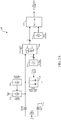
- Fig. 2A shows an illustrative embodiment of a system 200 for detecting tampering with a product.
- the system 200 comprises a current mirror 202, a current reference 204, a comparator array 206, voltage references 208, digital logic 210, a time reference 212, and a switchable capacitance array 214.
- a current I meas is injected into the device-under-test capacitor C DUT connected to the chip pins.
- a voltage difference ⁇ V at the capacitor observed in a time interval ⁇ T allows to determine the capacitance C DUT :
- C DUT I meas ⁇ T/ ⁇ V.
- the device-under-test capacitor is externally connected to two sensor pads.
- the current mirror 202 injects the current I meas into that capacitor.
- the array 206 of comparators detects when the voltage at the capacitor is crossing several reference voltages 208.
- the digital block 210 evaluates the linearity of the voltage slope on the device-under-test capacitor C DUT , using the voltage-crossing signals of the comparator array 206 as an input.
- a single comparator with a switchable reference voltage source could be used (not shown).
- a counter measures the time difference between subsequent reference voltage crossings to provide a measurement result.
- a configurable capacitor array 214 allows for a decreased input impedance.
- each voltage crossing marks the beginning of a new slope segment.
- This slope value may be compared with a predefined range of slope values, to determine whether it is not too steep or too flat. If the slope value falls within the predefined range, then the slope segment is a valid segment and can thus be used to calculate the capacitance C DUT ; otherwise it is an invalid segment and it is discarded.
- the counter value is stored in memory to be able to perform post-processing for providing the measurement result. It is noted that it is not necessary to restart the counter at each reception of a voltage-crossing signal. That is to say, the counter can be kept running without a reset and then later subtractions can be performed to obtain the ⁇ t value for each of the segments.
- a first condition for distinguishing valid segments from invalid segments is defined.
- a second condition is defined by determining whether the slope values of the slope segments, which satisfy the first condition, have substantially the same value. In this way, as mentioned above, valid measurement results are properly distinguished from invalid measurement results. Thus, the validity does not only depend on the steepness of a single segment being within a predefined range.
- the slope segments being within the allowed range i.e. the slope segments that are reasonably steep
- Fig. 2B shows an illustrative embodiment of a method 216 for detecting tampering with a product.
- the method 216 comprises the following steps.
- an integrated circuit IC injects a current in a capacitor comprised in or attached to a product.
- the IC detects a corresponding voltage slope on said capacitor.
- the IC divides said voltage slope into a plurality of slope segments.
- the IC discards a first set of slope segments, whose slope value falls outside a predefined range of slope values, and at 226, the IC uses a second set of slope segments, whose slope value falls within said predefined range, for determining a capacitance on the capacitor.
- the integrated circuit uses only those slope segments of the second set that have substantially the same slope value for determining the capacitance on the capacitor. In this way, valid measurement results are properly distinguished from invalid measurement results.
- Figs. 3A and 3B show an example of an undisturbed voltage slope 300 and an example of a disturbed voltage slope 302.
- Strong alternating current (AC) voltage disturbances in series to the device-under-test due to parasitic capacitive coupling from the reader coil can cause a clamping of the sensor input pins by the diodes to ground and supply (such diodes usually exist in CMOS technology). That clamping can deform the otherwise linear voltage slope at the sensor interface and cause wrong measurement results if no counter-measures are taken.
- Fig. 3B shows the voltage slope on the capacitor C DUT under influence of disturbances. The mean value (solid line) and the upper and lower peak values of the envelope (dashed lines) of the AC signal are shown. In a typical disturbance case 302, the measured slope steepness (dash-dotted line) is different from the undisturbed case 300. However, if only two measurement points are used, then a deformation of the slope cannot be detected.
- Fig. 4 shows an illustrative embodiment of a voltage slope divided into a plurality of slope segments 400.
- Fig. 4 shows a more specific embodiment of distinguishing valid slope segments from invalid slope segments.
- the voltage slope is divided into a plurality of segments. Slope segments that are too steep (e.g., due to strong clamping at ground diodes) and slope segments that are too flat (e.g., due to strong clamping at supply diodes) are discarded.
- segments 1 and 2 are too steep, and segments 5 and 6 are too flat.
- slope segments whose slope value falls within a predefined range of slope segments are used for determining the capacitance on the external capacitor.
- the integrated circuit comprises a configurable capacitor array switchably coupled to the capacitor, for reducing the input impedance of the capacitor. More specifically, adding internal capacitances in parallel to the external CDUT decreases the overall impedance at the capacitive sensor input. The lower the input impedance, the lower also the disturbance voltage at the sensor input due to parasitic capacitive coupling from the reader coil (capacitive divider of reader coil voltage). Therefore, by means of such an internal capacitor array the probability of invalid measurements due to high disturbances can be actively reduced.
- a fine granularity of the capacitor array C int allows to optimize the disturbance voltage reduction in function of the size of C DUT while avoiding time-outs.
- the systems and methods described herein may at least partially be embodied by a computer program or a plurality of computer programs, which may exist in a variety of forms both active and inactive in a single computer system or across multiple computer systems.
- they may exist as software program(s) comprised of program instructions in source code, object code, executable code or other formats for performing some of the steps.
- Any of the above may be embodied on a computer-readable medium, which may include storage devices and signals, in compressed or uncompressed form.
- the term "computer” refers to any electronic device comprising a processor, such as a general-purpose central processing unit (CPU), a specific-purpose processor or a microcontroller.
- a computer is capable of receiving data (an input), of performing a sequence of predetermined operations thereupon, and of producing thereby a result in the form of information or signals (an output).
- the term "computer” will mean either a processor in particular or more generally a processor in association with an assemblage of interrelated elements contained within a single case or housing.
- processor or “processing unit” refers to a data processing circuit that may be a microprocessor, a co-processor, a microcontroller, a microcomputer, a central processing unit, a field programmable gate array (FPGA), a programmable logic circuit, and/or any circuit that manipulates signals (analog or digital) based on operational instructions that are stored in a memory.
- memory refers to a storage circuit or multiple storage circuits such as read-only memory, random access memory, volatile memory, non-volatile memory, static memory, dynamic memory, Flash memory, cache memory, and/or any circuit that stores digital information.
- a "computer-readable medium” or “storage medium” may be any means that can contain, store, communicate, propagate, or transport a computer program for use by or in connection with the instruction execution system, apparatus, or device.
- the computer-readable medium may be, for example but not limited to, an electronic, magnetic, optical, electromagnetic, infrared, or semiconductor system, apparatus, device, or propagation medium.
- the computer-readable medium may include the following: an electrical connection having one or more wires, a portable computer diskette, a random-access memory (RAM), a read-only memory (ROM), an erasable programmable read-only memory (EPROM or Flash memory), an optical fiber, a portable compact disc read-only memory (CDROM), a digital versatile disc (DVD), a Blu-ray disc (BD), and a memory card.
- RAM random-access memory
- ROM read-only memory
- EPROM or Flash memory erasable programmable read-only memory
- CDROM compact disc read-only memory
- DVD digital versatile disc
- BD Blu-ray disc
Landscapes
- Engineering & Computer Science (AREA)
- Physics & Mathematics (AREA)
- General Physics & Mathematics (AREA)
- Computer Hardware Design (AREA)
- Microelectronics & Electronic Packaging (AREA)
- General Engineering & Computer Science (AREA)
- Theoretical Computer Science (AREA)
- Computer Security & Cryptography (AREA)
- Computer Networks & Wireless Communication (AREA)
- Automation & Control Theory (AREA)
- Electromagnetism (AREA)
- Environmental & Geological Engineering (AREA)
- Semiconductor Integrated Circuits (AREA)
- Tests Of Electronic Circuits (AREA)
- Storage Device Security (AREA)
Claims (15)
- System (200) zum Erkennen einer Manipulation eines Produkts, wobei das System Folgendes umfasst:einen Kondensator (CDUT), der im Produkt umfasst oder an ihm angebracht ist;eine integrierte Schaltung, die konfiguriert ist, um auf den Kondensator einen Strom aufzuschalten und eine entsprechende Spannungsflanke im Kondensator zu erkennen (218, 220);wobei die integrierte Schaltung ferner konfiguriert ist, um die Spannungsflanke in eine Vielzahl von Flankensegmenten zu unterteilen (222);wobei die integrierte Schaltung ferner konfiguriert ist, um eine erste Menge von Flankensegmenten, deren Flankenwert außerhalb eines vordefinierten Bereichs von Flankenwerten liegt, zu verwerfen (224);wobei die integrierte Schaltung ferner konfiguriert ist, um eine zweite Menge von Flankensegmenten, deren Flankenwert innerhalb des vordefinierten Bereichs liegt, zum Bestimmen der Kapazität im Kondensator zu nutzen (226) .
- System nach Anspruch 1, wobei die integrierte Schaltung ferner konfiguriert ist, um nur diejenigen Flankensegmente der zweiten Menge, die im Wesentlichen denselben Flankenwert aufweisen, zum Bestimmen der Kapazität im Kondensator zu nutzen.
- System nach Anspruch 1 oder 2, wobei die integrierte Schaltung eine Anordnung von Komparatoren zum Erkennen der Spannungsflanke im Kondensator umfasst.
- System nach Anspruch 1 oder 2, wobei die integrierte Schaltung einen Komparator mit einer schaltbaren Bezugsspannungsquelle zum Erkennen der Spannungsflanke im Kondensator umfasst.
- System nach einem vorhergehenden Anspruch, wobei die integrierte Schaltung ferner konfiguriert ist, um die Kapazität mit einem Bezugswert zu vergleichen, um die Manipulation des Produkts zu erkennen.
- System nach einem vorhergehenden Anspruch, wobei die integrierte Schaltung eine konfigurierbare Kondensatoranordnung, die schaltbar an den Kondensator gekoppelt ist, um die Eingangsimpedanz des Kondensators zu verringern, umfasst.
- System nach Anspruch 6, wobei die integrierte Schaltung konfiguriert ist, um die konfigurierbare Kondensatoranordnung mit dem Kondensator zu verbinden, wenn die Kapazität im Kondensator einen vordefinierten Schwellenwert unterschreitet.
- System nach Anspruch 7, wobei die integrierte Schaltung konfiguriert ist, um die konfigurierbare Kondensatoranordnung vom Kondensator zu trennen, wenn die Kapazität im Kondensator den vordefinierten Schwellenwert überschreitet.
- System nach einem vorhergehenden Anspruch, wobei die integrierte Schaltung in einem RFID-Transponder (RFID = Radio Frequency Identification) oder in einem NFC-Transponder (NFC = Near Field Communication) umfasst ist.
- Verfahren zum Erkennen einer Manipulation eines Produkts, wobei das Verfahren Folgendes umfasst:Aufschalten eines Stroms auf einen Kondensator, der im Produkt umfasst oder an ihm angebracht ist, durch eine integrierte Schaltung (218);Erkennen einer entsprechenden Spannungsflanke im Kondensator durch die integrierte Schaltung (220);Unterteilen der Spannungsflanke in eine Vielzahl von Flankensegmenten durch die integrierte Schaltung (222);Verwerfen einer ersten Menge von Flankensegmenten, deren Flankenwert außerhalb eines vordefinierten Bereichs von Flankenwerten liegt, durch die integrierte Schaltung (224);Nutzen einer zweiten Menge von Flankensegmenten, deren Flankenwert innerhalb des vordefinierten Bereichs liegt, durch die integrierte Schaltung zum Bestimmen der Kapazität im Kondensator (226).
- Verfahren nach Anspruch 10, wobei die integrierte Schaltung nur diejenigen Flankensegmente der zweiten Menge, die im Wesentlichen denselben Flankenwert aufweisen, zum Bestimmen der Kapazität im Kondensator nutzt.
- Verfahren nach Anspruch 10 oder 11, wobei die integrierte Schaltung eine konfigurierbare Kondensatoranordnung, die schaltbar an den Kondensator gekoppelt ist, um die Eingangsimpedanz des Kondensators zu verringern, umfasst.
- Verfahren nach Anspruch 12, wobei die integrierte Schaltung die konfigurierbare Kondensatoranordnung mit dem Kondensator verbindet, wenn die Kapazität im Kondensator einen vordefinierten Schwellenwert unterschreitet.
- Computerprogramm, das Anweisungen, durch die, wenn sie ausgeführt werden, das Verfahren nach einem der Ansprüche 10 bis 13 ausgeführt oder gesteuert wird, umfasst.
- Nichtflüchtiges, computerlesbares Medium, das das Computerprogramm nach Anspruch 14 umfasst.
Priority Applications (3)
| Application Number | Priority Date | Filing Date | Title |
|---|---|---|---|
| EP18192899.5A EP3621047B1 (de) | 2018-09-06 | 2018-09-06 | System und verfahren zum erkennen von manipulationen an einem produkt |
| US16/552,578 US10929739B2 (en) | 2018-09-06 | 2019-08-27 | System and method for detecting tampering with a product |
| CN201910830631.9A CN110879346B (zh) | 2018-09-06 | 2019-09-02 | 用于检测对产品的篡改的系统和方法 |
Applications Claiming Priority (1)
| Application Number | Priority Date | Filing Date | Title |
|---|---|---|---|
| EP18192899.5A EP3621047B1 (de) | 2018-09-06 | 2018-09-06 | System und verfahren zum erkennen von manipulationen an einem produkt |
Publications (2)
| Publication Number | Publication Date |
|---|---|
| EP3621047A1 EP3621047A1 (de) | 2020-03-11 |
| EP3621047B1 true EP3621047B1 (de) | 2021-04-28 |
Family
ID=63528532
Family Applications (1)
| Application Number | Title | Priority Date | Filing Date |
|---|---|---|---|
| EP18192899.5A Active EP3621047B1 (de) | 2018-09-06 | 2018-09-06 | System und verfahren zum erkennen von manipulationen an einem produkt |
Country Status (3)
| Country | Link |
|---|---|
| US (1) | US10929739B2 (de) |
| EP (1) | EP3621047B1 (de) |
| CN (1) | CN110879346B (de) |
Families Citing this family (4)
| Publication number | Priority date | Publication date | Assignee | Title |
|---|---|---|---|---|
| US10819616B2 (en) * | 2019-01-15 | 2020-10-27 | Litepoint Corporation | System and method for testing a data packet signal transceiver |
| EP3786912B1 (de) | 2019-08-27 | 2023-12-06 | Nxp B.V. | Integrierte schaltung und messverfahren |
| US10977539B1 (en) | 2019-12-20 | 2021-04-13 | Capital One Services, Llc | Systems and methods for use of capacitive member to prevent chip fraud |
| US20240223082A1 (en) * | 2023-01-04 | 2024-07-04 | Texas Instruments Incorporated | Determination of values indicative of multiple passive components connected to a device pin |
Family Cites Families (25)
| Publication number | Priority date | Publication date | Assignee | Title |
|---|---|---|---|---|
| US4885571A (en) * | 1986-04-15 | 1989-12-05 | B. I. Incorperated | Tag for use with personnel monitoring system |
| US5298884A (en) * | 1992-10-16 | 1994-03-29 | Bi Incorporated | Tamper detection circuit and method for use with wearable transmitter tag |
| GB9914711D0 (en) * | 1999-06-23 | 1999-08-25 | Leck Michael J | Electronic seal,methods and security system |
| US7017807B2 (en) * | 2003-09-08 | 2006-03-28 | Francis M. Claessens | Apparatus and method for detecting tampering with containers and preventing counterfeiting thereof |
| US7152804B1 (en) * | 2004-03-15 | 2006-12-26 | Kovlo, Inc. | MOS electronic article surveillance, RF and/or RF identification tag/device, and methods for making and using the same |
| EP1807797B1 (de) * | 2004-10-28 | 2016-12-21 | Assa Abloy Ab | Sicherheits-versiegelungseinrichtung mit einem rfid-etikett |
| KR100855854B1 (ko) * | 2006-04-24 | 2008-09-01 | 주식회사 하이닉스반도체 | 불휘발성 강유전체 메모리를 포함하는 rfid에서의파워-온 리셋 회로 |
| US20080143519A1 (en) * | 2006-12-19 | 2008-06-19 | 3M Innovative Properties Company | Tamper-indicating radio frequency identification tag and methods of indicating tampering of a radio frequency identification tag |
| US7830157B2 (en) * | 2007-12-28 | 2010-11-09 | 3M Innovative Properties Company | Pulsed capacitance measuring circuits and methods |
| US7952478B2 (en) * | 2008-07-29 | 2011-05-31 | International Business Machines Corporation | Capacitance-based microchip exploitation detection |
| US7989918B2 (en) * | 2009-01-26 | 2011-08-02 | International Business Machines Corporation | Implementing tamper evident and resistant detection through modulation of capacitance |
| CN101795070B (zh) * | 2010-04-02 | 2012-09-05 | 日银Imp微电子有限公司 | 一种线性调节斜坡补偿电压斜率的系统 |
| PL2437403T3 (pl) * | 2010-09-30 | 2013-08-30 | Legic Identsystems Ag | Wykrywanie bezstykowego urządzenia pamięciowego danych |
| US9041687B2 (en) * | 2011-12-07 | 2015-05-26 | Htc Corporation | Communication method for capacitive touch panel |
| US9018972B1 (en) * | 2012-06-04 | 2015-04-28 | Sandia Corporation | Area-efficient physically unclonable function circuit architecture |
| CN103630735B (zh) * | 2012-08-27 | 2016-04-13 | 上海占空比电子科技有限公司 | 一种电压斜率变化检测电路及方法 |
| US10181751B2 (en) * | 2012-10-18 | 2019-01-15 | Telefonaktiebolaget Lm Ericsson (Publ) | Device and method for power disturbance detection |
| FR3005815B1 (fr) * | 2013-05-17 | 2019-09-20 | Thales | Systeme de generation d'un signal analogique |
| US9542637B2 (en) | 2014-12-31 | 2017-01-10 | Intermec, Inc. | RFID tag with anti-tamper assembly |
| CN204564349U (zh) * | 2015-04-16 | 2015-08-19 | 杭州天明电子有限公司 | 一种高压直流除尘系统及其脉冲高压电源 |
| EP3145092B1 (de) * | 2015-09-21 | 2019-06-19 | STMicroelectronics International N.V. | Verfahren und senderschaltung zur kommunikation mit aktiver belastungsmodulation in rfid-systemen |
| CN106557805A (zh) * | 2015-09-24 | 2017-04-05 | 葛兰菲安全有限公司 | 安全无线射频识别卷标、系统及其方法 |
| CN206470362U (zh) * | 2016-11-04 | 2017-09-05 | 深圳市沃特玛电池有限公司 | 一种告警电路 |
| EP3364333B1 (de) * | 2017-02-17 | 2022-04-06 | Nxp B.V. | Elektronische manipulationserkennungsvorrichtung |
| CN108305659B (zh) * | 2018-02-27 | 2020-08-25 | 上海贝岭股份有限公司 | 非易失存储器擦写电压的斜率控制电路及非易失存储器 |
-
2018
- 2018-09-06 EP EP18192899.5A patent/EP3621047B1/de active Active
-
2019
- 2019-08-27 US US16/552,578 patent/US10929739B2/en active Active
- 2019-09-02 CN CN201910830631.9A patent/CN110879346B/zh active Active
Non-Patent Citations (1)
| Title |
|---|
| None * |
Also Published As
| Publication number | Publication date |
|---|---|
| EP3621047A1 (de) | 2020-03-11 |
| US10929739B2 (en) | 2021-02-23 |
| CN110879346A (zh) | 2020-03-13 |
| CN110879346B (zh) | 2024-04-23 |
| US20200082238A1 (en) | 2020-03-12 |
Similar Documents
| Publication | Publication Date | Title |
|---|---|---|
| US10929739B2 (en) | System and method for detecting tampering with a product | |
| US10945210B2 (en) | Control system for a radio frequency communication device | |
| US11313702B2 (en) | System and method for monitoring analog front-end (AFE) circuitry of an inductive position sensor | |
| CN101295345B (zh) | 射频识别读取装置 | |
| US8907683B2 (en) | Detection of a contactless data storage device | |
| US20110196628A1 (en) | Deterioration detection circuit | |
| US11295093B2 (en) | Transponder and method of operating the same | |
| US9471792B2 (en) | Detection arrangement | |
| CN105954696B (zh) | 一种传感器校正方法、装置和电子设备 | |
| US11500003B2 (en) | Integrated circuit and measurement method | |
| US20230318313A1 (en) | Battery type determination system, method for determining battery type, and storage medium | |
| US11199621B2 (en) | Clock-stop frequency adjustment for a transponder | |
| US20240333288A1 (en) | Key detection method and system | |
| US11860207B2 (en) | Determining electric field distributions | |
| US20080012574A1 (en) | Qualifying of a detector of noise peaks in the supply of an integrated circuit | |
| KR102391928B1 (ko) | 복합 감지 장치 및 동작 방법과, 이를 이용한 도어락 시스템 | |
| KR910006827A (ko) | 로우 밧데리의 상태를 검출하는 기능을 갖는 컴퓨터 | |
| US20180285601A1 (en) | Mpu protection device | |
| KR20180118298A (ko) | 전자기파를 측정하기 위한 감지 장치 및 측정 시스템 | |
| KR20140138195A (ko) | 알에프아이디 라벨용 데이터 감지 회로 | |
| KR20160148385A (ko) | 웨이크업 검출 회로 및 그를 이용한 전자 가격 표시기 |
Legal Events
| Date | Code | Title | Description |
|---|---|---|---|
| PUAI | Public reference made under article 153(3) epc to a published international application that has entered the european phase |
Free format text: ORIGINAL CODE: 0009012 |
|
| STAA | Information on the status of an ep patent application or granted ep patent |
Free format text: STATUS: THE APPLICATION HAS BEEN PUBLISHED |
|
| AK | Designated contracting states |
Kind code of ref document: A1 Designated state(s): AL AT BE BG CH CY CZ DE DK EE ES FI FR GB GR HR HU IE IS IT LI LT LU LV MC MK MT NL NO PL PT RO RS SE SI SK SM TR |
|
| AX | Request for extension of the european patent |
Extension state: BA ME |
|
| STAA | Information on the status of an ep patent application or granted ep patent |
Free format text: STATUS: REQUEST FOR EXAMINATION WAS MADE |
|
| 17P | Request for examination filed |
Effective date: 20200911 |
|
| RBV | Designated contracting states (corrected) |
Designated state(s): AL AT BE BG CH CY CZ DE DK EE ES FI FR GB GR HR HU IE IS IT LI LT LU LV MC MK MT NL NO PL PT RO RS SE SI SK SM TR |
|
| GRAP | Despatch of communication of intention to grant a patent |
Free format text: ORIGINAL CODE: EPIDOSNIGR1 |
|
| STAA | Information on the status of an ep patent application or granted ep patent |
Free format text: STATUS: GRANT OF PATENT IS INTENDED |
|
| INTG | Intention to grant announced |
Effective date: 20210205 |
|
| RAP1 | Party data changed (applicant data changed or rights of an application transferred) |
Owner name: NXP B.V. |
|
| GRAS | Grant fee paid |
Free format text: ORIGINAL CODE: EPIDOSNIGR3 |
|
| GRAA | (expected) grant |
Free format text: ORIGINAL CODE: 0009210 |
|
| STAA | Information on the status of an ep patent application or granted ep patent |
Free format text: STATUS: THE PATENT HAS BEEN GRANTED |
|
| AK | Designated contracting states |
Kind code of ref document: B1 Designated state(s): AL AT BE BG CH CY CZ DE DK EE ES FI FR GB GR HR HU IE IS IT LI LT LU LV MC MK MT NL NO PL PT RO RS SE SI SK SM TR |
|
| REG | Reference to a national code |
Ref country code: GB Ref legal event code: FG4D |
|
| REG | Reference to a national code |
Ref country code: CH Ref legal event code: EP |
|
| REG | Reference to a national code |
Ref country code: AT Ref legal event code: REF Ref document number: 1387967 Country of ref document: AT Kind code of ref document: T Effective date: 20210515 |
|
| REG | Reference to a national code |
Ref country code: DE Ref legal event code: R096 Ref document number: 602018016112 Country of ref document: DE |
|
| REG | Reference to a national code |
Ref country code: IE Ref legal event code: FG4D |
|
| REG | Reference to a national code |
Ref country code: LT Ref legal event code: MG9D |
|
| REG | Reference to a national code |
Ref country code: AT Ref legal event code: MK05 Ref document number: 1387967 Country of ref document: AT Kind code of ref document: T Effective date: 20210428 |
|
| PG25 | Lapsed in a contracting state [announced via postgrant information from national office to epo] |
Ref country code: FI Free format text: LAPSE BECAUSE OF FAILURE TO SUBMIT A TRANSLATION OF THE DESCRIPTION OR TO PAY THE FEE WITHIN THE PRESCRIBED TIME-LIMIT Effective date: 20210428 Ref country code: HR Free format text: LAPSE BECAUSE OF FAILURE TO SUBMIT A TRANSLATION OF THE DESCRIPTION OR TO PAY THE FEE WITHIN THE PRESCRIBED TIME-LIMIT Effective date: 20210428 Ref country code: LT Free format text: LAPSE BECAUSE OF FAILURE TO SUBMIT A TRANSLATION OF THE DESCRIPTION OR TO PAY THE FEE WITHIN THE PRESCRIBED TIME-LIMIT Effective date: 20210428 Ref country code: NL Free format text: LAPSE BECAUSE OF FAILURE TO SUBMIT A TRANSLATION OF THE DESCRIPTION OR TO PAY THE FEE WITHIN THE PRESCRIBED TIME-LIMIT Effective date: 20210428 Ref country code: BG Free format text: LAPSE BECAUSE OF FAILURE TO SUBMIT A TRANSLATION OF THE DESCRIPTION OR TO PAY THE FEE WITHIN THE PRESCRIBED TIME-LIMIT Effective date: 20210728 Ref country code: AT Free format text: LAPSE BECAUSE OF FAILURE TO SUBMIT A TRANSLATION OF THE DESCRIPTION OR TO PAY THE FEE WITHIN THE PRESCRIBED TIME-LIMIT Effective date: 20210428 |
|
| PG25 | Lapsed in a contracting state [announced via postgrant information from national office to epo] |
Ref country code: PL Free format text: LAPSE BECAUSE OF FAILURE TO SUBMIT A TRANSLATION OF THE DESCRIPTION OR TO PAY THE FEE WITHIN THE PRESCRIBED TIME-LIMIT Effective date: 20210428 Ref country code: NO Free format text: LAPSE BECAUSE OF FAILURE TO SUBMIT A TRANSLATION OF THE DESCRIPTION OR TO PAY THE FEE WITHIN THE PRESCRIBED TIME-LIMIT Effective date: 20210728 Ref country code: LV Free format text: LAPSE BECAUSE OF FAILURE TO SUBMIT A TRANSLATION OF THE DESCRIPTION OR TO PAY THE FEE WITHIN THE PRESCRIBED TIME-LIMIT Effective date: 20210428 Ref country code: PT Free format text: LAPSE BECAUSE OF FAILURE TO SUBMIT A TRANSLATION OF THE DESCRIPTION OR TO PAY THE FEE WITHIN THE PRESCRIBED TIME-LIMIT Effective date: 20210830 Ref country code: SE Free format text: LAPSE BECAUSE OF FAILURE TO SUBMIT A TRANSLATION OF THE DESCRIPTION OR TO PAY THE FEE WITHIN THE PRESCRIBED TIME-LIMIT Effective date: 20210428 Ref country code: RS Free format text: LAPSE BECAUSE OF FAILURE TO SUBMIT A TRANSLATION OF THE DESCRIPTION OR TO PAY THE FEE WITHIN THE PRESCRIBED TIME-LIMIT Effective date: 20210428 Ref country code: IS Free format text: LAPSE BECAUSE OF FAILURE TO SUBMIT A TRANSLATION OF THE DESCRIPTION OR TO PAY THE FEE WITHIN THE PRESCRIBED TIME-LIMIT Effective date: 20210828 Ref country code: GR Free format text: LAPSE BECAUSE OF FAILURE TO SUBMIT A TRANSLATION OF THE DESCRIPTION OR TO PAY THE FEE WITHIN THE PRESCRIBED TIME-LIMIT Effective date: 20210729 |
|
| REG | Reference to a national code |
Ref country code: NL Ref legal event code: MP Effective date: 20210428 |
|
| PG25 | Lapsed in a contracting state [announced via postgrant information from national office to epo] |
Ref country code: RO Free format text: LAPSE BECAUSE OF FAILURE TO SUBMIT A TRANSLATION OF THE DESCRIPTION OR TO PAY THE FEE WITHIN THE PRESCRIBED TIME-LIMIT Effective date: 20210428 Ref country code: DK Free format text: LAPSE BECAUSE OF FAILURE TO SUBMIT A TRANSLATION OF THE DESCRIPTION OR TO PAY THE FEE WITHIN THE PRESCRIBED TIME-LIMIT Effective date: 20210428 Ref country code: CZ Free format text: LAPSE BECAUSE OF FAILURE TO SUBMIT A TRANSLATION OF THE DESCRIPTION OR TO PAY THE FEE WITHIN THE PRESCRIBED TIME-LIMIT Effective date: 20210428 Ref country code: SM Free format text: LAPSE BECAUSE OF FAILURE TO SUBMIT A TRANSLATION OF THE DESCRIPTION OR TO PAY THE FEE WITHIN THE PRESCRIBED TIME-LIMIT Effective date: 20210428 Ref country code: SK Free format text: LAPSE BECAUSE OF FAILURE TO SUBMIT A TRANSLATION OF THE DESCRIPTION OR TO PAY THE FEE WITHIN THE PRESCRIBED TIME-LIMIT Effective date: 20210428 Ref country code: ES Free format text: LAPSE BECAUSE OF FAILURE TO SUBMIT A TRANSLATION OF THE DESCRIPTION OR TO PAY THE FEE WITHIN THE PRESCRIBED TIME-LIMIT Effective date: 20210428 Ref country code: EE Free format text: LAPSE BECAUSE OF FAILURE TO SUBMIT A TRANSLATION OF THE DESCRIPTION OR TO PAY THE FEE WITHIN THE PRESCRIBED TIME-LIMIT Effective date: 20210428 |
|
| REG | Reference to a national code |
Ref country code: DE Ref legal event code: R097 Ref document number: 602018016112 Country of ref document: DE |
|
| PLBE | No opposition filed within time limit |
Free format text: ORIGINAL CODE: 0009261 |
|
| STAA | Information on the status of an ep patent application or granted ep patent |
Free format text: STATUS: NO OPPOSITION FILED WITHIN TIME LIMIT |
|
| 26N | No opposition filed |
Effective date: 20220131 |
|
| REG | Reference to a national code |
Ref country code: CH Ref legal event code: PL |
|
| REG | Reference to a national code |
Ref country code: BE Ref legal event code: MM Effective date: 20210930 |
|
| PG25 | Lapsed in a contracting state [announced via postgrant information from national office to epo] |
Ref country code: IS Free format text: LAPSE BECAUSE OF FAILURE TO SUBMIT A TRANSLATION OF THE DESCRIPTION OR TO PAY THE FEE WITHIN THE PRESCRIBED TIME-LIMIT Effective date: 20210828 Ref country code: MC Free format text: LAPSE BECAUSE OF FAILURE TO SUBMIT A TRANSLATION OF THE DESCRIPTION OR TO PAY THE FEE WITHIN THE PRESCRIBED TIME-LIMIT Effective date: 20210428 Ref country code: AL Free format text: LAPSE BECAUSE OF FAILURE TO SUBMIT A TRANSLATION OF THE DESCRIPTION OR TO PAY THE FEE WITHIN THE PRESCRIBED TIME-LIMIT Effective date: 20210428 |
|
| PG25 | Lapsed in a contracting state [announced via postgrant information from national office to epo] |
Ref country code: LU Free format text: LAPSE BECAUSE OF NON-PAYMENT OF DUE FEES Effective date: 20210906 Ref country code: IT Free format text: LAPSE BECAUSE OF FAILURE TO SUBMIT A TRANSLATION OF THE DESCRIPTION OR TO PAY THE FEE WITHIN THE PRESCRIBED TIME-LIMIT Effective date: 20210428 Ref country code: IE Free format text: LAPSE BECAUSE OF NON-PAYMENT OF DUE FEES Effective date: 20210906 Ref country code: BE Free format text: LAPSE BECAUSE OF NON-PAYMENT OF DUE FEES Effective date: 20210930 |
|
| PG25 | Lapsed in a contracting state [announced via postgrant information from national office to epo] |
Ref country code: LI Free format text: LAPSE BECAUSE OF NON-PAYMENT OF DUE FEES Effective date: 20210930 Ref country code: CH Free format text: LAPSE BECAUSE OF NON-PAYMENT OF DUE FEES Effective date: 20210930 |
|
| GBPC | Gb: european patent ceased through non-payment of renewal fee |
Effective date: 20220906 |
|
| PG25 | Lapsed in a contracting state [announced via postgrant information from national office to epo] |
Ref country code: CY Free format text: LAPSE BECAUSE OF FAILURE TO SUBMIT A TRANSLATION OF THE DESCRIPTION OR TO PAY THE FEE WITHIN THE PRESCRIBED TIME-LIMIT Effective date: 20210428 |
|
| PG25 | Lapsed in a contracting state [announced via postgrant information from national office to epo] |
Ref country code: HU Free format text: LAPSE BECAUSE OF FAILURE TO SUBMIT A TRANSLATION OF THE DESCRIPTION OR TO PAY THE FEE WITHIN THE PRESCRIBED TIME-LIMIT; INVALID AB INITIO Effective date: 20180906 |
|
| P01 | Opt-out of the competence of the unified patent court (upc) registered |
Effective date: 20230725 |
|
| PG25 | Lapsed in a contracting state [announced via postgrant information from national office to epo] |
Ref country code: GB Free format text: LAPSE BECAUSE OF NON-PAYMENT OF DUE FEES Effective date: 20220906 |
|
| PG25 | Lapsed in a contracting state [announced via postgrant information from national office to epo] |
Ref country code: MK Free format text: LAPSE BECAUSE OF FAILURE TO SUBMIT A TRANSLATION OF THE DESCRIPTION OR TO PAY THE FEE WITHIN THE PRESCRIBED TIME-LIMIT Effective date: 20210428 |
|
| PG25 | Lapsed in a contracting state [announced via postgrant information from national office to epo] |
Ref country code: MT Free format text: LAPSE BECAUSE OF FAILURE TO SUBMIT A TRANSLATION OF THE DESCRIPTION OR TO PAY THE FEE WITHIN THE PRESCRIBED TIME-LIMIT Effective date: 20210428 |
|
| PGFP | Annual fee paid to national office [announced via postgrant information from national office to epo] |
Ref country code: DE Payment date: 20250820 Year of fee payment: 8 |
|
| PGFP | Annual fee paid to national office [announced via postgrant information from national office to epo] |
Ref country code: FR Payment date: 20250820 Year of fee payment: 8 |
|
| PG25 | Lapsed in a contracting state [announced via postgrant information from national office to epo] |
Ref country code: TR Free format text: LAPSE BECAUSE OF FAILURE TO SUBMIT A TRANSLATION OF THE DESCRIPTION OR TO PAY THE FEE WITHIN THE PRESCRIBED TIME-LIMIT Effective date: 20210428 |