EP3621060A1 - Procédé d'attaque de circuit de pixels - Google Patents
Procédé d'attaque de circuit de pixels Download PDFInfo
- Publication number
- EP3621060A1 EP3621060A1 EP17899228.5A EP17899228A EP3621060A1 EP 3621060 A1 EP3621060 A1 EP 3621060A1 EP 17899228 A EP17899228 A EP 17899228A EP 3621060 A1 EP3621060 A1 EP 3621060A1
- Authority
- EP
- European Patent Office
- Prior art keywords
- voltage
- transistor
- drive transistor
- electrode
- compensation
- Prior art date
- Legal status (The legal status is an assumption and is not a legal conclusion. Google has not performed a legal analysis and makes no representation as to the accuracy of the status listed.)
- Pending
Links
- 238000000034 method Methods 0.000 title claims abstract description 38
- 239000003990 capacitor Substances 0.000 claims description 26
- 230000000630 rising effect Effects 0.000 claims description 6
- 238000007667 floating Methods 0.000 claims description 5
- 238000010586 diagram Methods 0.000 description 18
- 230000000694 effects Effects 0.000 description 9
- 229920001621 AMOLED Polymers 0.000 description 6
- 208000033361 autosomal recessive with axonal neuropathy 2 spinocerebellar ataxia Diseases 0.000 description 5
- 230000008569 process Effects 0.000 description 5
- 238000004364 calculation method Methods 0.000 description 4
- 230000007246 mechanism Effects 0.000 description 3
- 230000008901 benefit Effects 0.000 description 2
- 230000008859 change Effects 0.000 description 2
- 230000001276 controlling effect Effects 0.000 description 2
- 230000002596 correlated effect Effects 0.000 description 2
- 238000005516 engineering process Methods 0.000 description 2
- 230000000087 stabilizing effect Effects 0.000 description 2
- 239000000758 substrate Substances 0.000 description 2
- 230000003044 adaptive effect Effects 0.000 description 1
- 230000008878 coupling Effects 0.000 description 1
- 238000010168 coupling process Methods 0.000 description 1
- 238000005859 coupling reaction Methods 0.000 description 1
- 239000004973 liquid crystal related substance Substances 0.000 description 1
- 230000007774 longterm Effects 0.000 description 1
- 238000004519 manufacturing process Methods 0.000 description 1
- 239000000463 material Substances 0.000 description 1
- 230000004048 modification Effects 0.000 description 1
- 238000012986 modification Methods 0.000 description 1
- 238000012797 qualification Methods 0.000 description 1
- 239000002096 quantum dot Substances 0.000 description 1
- 230000004044 response Effects 0.000 description 1
- 239000010409 thin film Substances 0.000 description 1
Images


Classifications
-
- G—PHYSICS
- G09—EDUCATION; CRYPTOGRAPHY; DISPLAY; ADVERTISING; SEALS
- G09G—ARRANGEMENTS OR CIRCUITS FOR CONTROL OF INDICATING DEVICES USING STATIC MEANS TO PRESENT VARIABLE INFORMATION
- G09G3/00—Control arrangements or circuits, of interest only in connection with visual indicators other than cathode-ray tubes
- G09G3/20—Control arrangements or circuits, of interest only in connection with visual indicators other than cathode-ray tubes for presentation of an assembly of a number of characters, e.g. a page, by composing the assembly by combination of individual elements arranged in a matrix no fixed position being assigned to or needed to be assigned to the individual characters or partial characters
- G09G3/22—Control arrangements or circuits, of interest only in connection with visual indicators other than cathode-ray tubes for presentation of an assembly of a number of characters, e.g. a page, by composing the assembly by combination of individual elements arranged in a matrix no fixed position being assigned to or needed to be assigned to the individual characters or partial characters using controlled light sources
- G09G3/30—Control arrangements or circuits, of interest only in connection with visual indicators other than cathode-ray tubes for presentation of an assembly of a number of characters, e.g. a page, by composing the assembly by combination of individual elements arranged in a matrix no fixed position being assigned to or needed to be assigned to the individual characters or partial characters using controlled light sources using electroluminescent panels
- G09G3/32—Control arrangements or circuits, of interest only in connection with visual indicators other than cathode-ray tubes for presentation of an assembly of a number of characters, e.g. a page, by composing the assembly by combination of individual elements arranged in a matrix no fixed position being assigned to or needed to be assigned to the individual characters or partial characters using controlled light sources using electroluminescent panels semiconductive, e.g. using light-emitting diodes [LED]
- G09G3/3208—Control arrangements or circuits, of interest only in connection with visual indicators other than cathode-ray tubes for presentation of an assembly of a number of characters, e.g. a page, by composing the assembly by combination of individual elements arranged in a matrix no fixed position being assigned to or needed to be assigned to the individual characters or partial characters using controlled light sources using electroluminescent panels semiconductive, e.g. using light-emitting diodes [LED] organic, e.g. using organic light-emitting diodes [OLED]
- G09G3/3225—Control arrangements or circuits, of interest only in connection with visual indicators other than cathode-ray tubes for presentation of an assembly of a number of characters, e.g. a page, by composing the assembly by combination of individual elements arranged in a matrix no fixed position being assigned to or needed to be assigned to the individual characters or partial characters using controlled light sources using electroluminescent panels semiconductive, e.g. using light-emitting diodes [LED] organic, e.g. using organic light-emitting diodes [OLED] using an active matrix
-
- G—PHYSICS
- G09—EDUCATION; CRYPTOGRAPHY; DISPLAY; ADVERTISING; SEALS
- G09G—ARRANGEMENTS OR CIRCUITS FOR CONTROL OF INDICATING DEVICES USING STATIC MEANS TO PRESENT VARIABLE INFORMATION
- G09G3/00—Control arrangements or circuits, of interest only in connection with visual indicators other than cathode-ray tubes
- G09G3/20—Control arrangements or circuits, of interest only in connection with visual indicators other than cathode-ray tubes for presentation of an assembly of a number of characters, e.g. a page, by composing the assembly by combination of individual elements arranged in a matrix no fixed position being assigned to or needed to be assigned to the individual characters or partial characters
- G09G3/22—Control arrangements or circuits, of interest only in connection with visual indicators other than cathode-ray tubes for presentation of an assembly of a number of characters, e.g. a page, by composing the assembly by combination of individual elements arranged in a matrix no fixed position being assigned to or needed to be assigned to the individual characters or partial characters using controlled light sources
- G09G3/30—Control arrangements or circuits, of interest only in connection with visual indicators other than cathode-ray tubes for presentation of an assembly of a number of characters, e.g. a page, by composing the assembly by combination of individual elements arranged in a matrix no fixed position being assigned to or needed to be assigned to the individual characters or partial characters using controlled light sources using electroluminescent panels
- G09G3/32—Control arrangements or circuits, of interest only in connection with visual indicators other than cathode-ray tubes for presentation of an assembly of a number of characters, e.g. a page, by composing the assembly by combination of individual elements arranged in a matrix no fixed position being assigned to or needed to be assigned to the individual characters or partial characters using controlled light sources using electroluminescent panels semiconductive, e.g. using light-emitting diodes [LED]
- G09G3/3208—Control arrangements or circuits, of interest only in connection with visual indicators other than cathode-ray tubes for presentation of an assembly of a number of characters, e.g. a page, by composing the assembly by combination of individual elements arranged in a matrix no fixed position being assigned to or needed to be assigned to the individual characters or partial characters using controlled light sources using electroluminescent panels semiconductive, e.g. using light-emitting diodes [LED] organic, e.g. using organic light-emitting diodes [OLED]
- G09G3/3225—Control arrangements or circuits, of interest only in connection with visual indicators other than cathode-ray tubes for presentation of an assembly of a number of characters, e.g. a page, by composing the assembly by combination of individual elements arranged in a matrix no fixed position being assigned to or needed to be assigned to the individual characters or partial characters using controlled light sources using electroluminescent panels semiconductive, e.g. using light-emitting diodes [LED] organic, e.g. using organic light-emitting diodes [OLED] using an active matrix
- G09G3/3233—Control arrangements or circuits, of interest only in connection with visual indicators other than cathode-ray tubes for presentation of an assembly of a number of characters, e.g. a page, by composing the assembly by combination of individual elements arranged in a matrix no fixed position being assigned to or needed to be assigned to the individual characters or partial characters using controlled light sources using electroluminescent panels semiconductive, e.g. using light-emitting diodes [LED] organic, e.g. using organic light-emitting diodes [OLED] using an active matrix with pixel circuitry controlling the current through the light-emitting element
-
- G—PHYSICS
- G09—EDUCATION; CRYPTOGRAPHY; DISPLAY; ADVERTISING; SEALS
- G09G—ARRANGEMENTS OR CIRCUITS FOR CONTROL OF INDICATING DEVICES USING STATIC MEANS TO PRESENT VARIABLE INFORMATION
- G09G3/00—Control arrangements or circuits, of interest only in connection with visual indicators other than cathode-ray tubes
- G09G3/20—Control arrangements or circuits, of interest only in connection with visual indicators other than cathode-ray tubes for presentation of an assembly of a number of characters, e.g. a page, by composing the assembly by combination of individual elements arranged in a matrix no fixed position being assigned to or needed to be assigned to the individual characters or partial characters
- G09G3/22—Control arrangements or circuits, of interest only in connection with visual indicators other than cathode-ray tubes for presentation of an assembly of a number of characters, e.g. a page, by composing the assembly by combination of individual elements arranged in a matrix no fixed position being assigned to or needed to be assigned to the individual characters or partial characters using controlled light sources
- G09G3/30—Control arrangements or circuits, of interest only in connection with visual indicators other than cathode-ray tubes for presentation of an assembly of a number of characters, e.g. a page, by composing the assembly by combination of individual elements arranged in a matrix no fixed position being assigned to or needed to be assigned to the individual characters or partial characters using controlled light sources using electroluminescent panels
- G09G3/32—Control arrangements or circuits, of interest only in connection with visual indicators other than cathode-ray tubes for presentation of an assembly of a number of characters, e.g. a page, by composing the assembly by combination of individual elements arranged in a matrix no fixed position being assigned to or needed to be assigned to the individual characters or partial characters using controlled light sources using electroluminescent panels semiconductive, e.g. using light-emitting diodes [LED]
- G09G3/3208—Control arrangements or circuits, of interest only in connection with visual indicators other than cathode-ray tubes for presentation of an assembly of a number of characters, e.g. a page, by composing the assembly by combination of individual elements arranged in a matrix no fixed position being assigned to or needed to be assigned to the individual characters or partial characters using controlled light sources using electroluminescent panels semiconductive, e.g. using light-emitting diodes [LED] organic, e.g. using organic light-emitting diodes [OLED]
- G09G3/3225—Control arrangements or circuits, of interest only in connection with visual indicators other than cathode-ray tubes for presentation of an assembly of a number of characters, e.g. a page, by composing the assembly by combination of individual elements arranged in a matrix no fixed position being assigned to or needed to be assigned to the individual characters or partial characters using controlled light sources using electroluminescent panels semiconductive, e.g. using light-emitting diodes [LED] organic, e.g. using organic light-emitting diodes [OLED] using an active matrix
- G09G3/3258—Control arrangements or circuits, of interest only in connection with visual indicators other than cathode-ray tubes for presentation of an assembly of a number of characters, e.g. a page, by composing the assembly by combination of individual elements arranged in a matrix no fixed position being assigned to or needed to be assigned to the individual characters or partial characters using controlled light sources using electroluminescent panels semiconductive, e.g. using light-emitting diodes [LED] organic, e.g. using organic light-emitting diodes [OLED] using an active matrix with pixel circuitry controlling the voltage across the light-emitting element
-
- G—PHYSICS
- G09—EDUCATION; CRYPTOGRAPHY; DISPLAY; ADVERTISING; SEALS
- G09G—ARRANGEMENTS OR CIRCUITS FOR CONTROL OF INDICATING DEVICES USING STATIC MEANS TO PRESENT VARIABLE INFORMATION
- G09G2230/00—Details of flat display driving waveforms
-
- G—PHYSICS
- G09—EDUCATION; CRYPTOGRAPHY; DISPLAY; ADVERTISING; SEALS
- G09G—ARRANGEMENTS OR CIRCUITS FOR CONTROL OF INDICATING DEVICES USING STATIC MEANS TO PRESENT VARIABLE INFORMATION
- G09G2300/00—Aspects of the constitution of display devices
- G09G2300/04—Structural and physical details of display devices
- G09G2300/0404—Matrix technologies
- G09G2300/0417—Special arrangements specific to the use of low carrier mobility technology
-
- G—PHYSICS
- G09—EDUCATION; CRYPTOGRAPHY; DISPLAY; ADVERTISING; SEALS
- G09G—ARRANGEMENTS OR CIRCUITS FOR CONTROL OF INDICATING DEVICES USING STATIC MEANS TO PRESENT VARIABLE INFORMATION
- G09G2300/00—Aspects of the constitution of display devices
- G09G2300/04—Structural and physical details of display devices
- G09G2300/0421—Structural details of the set of electrodes
- G09G2300/043—Compensation electrodes or other additional electrodes in matrix displays related to distortions or compensation signals, e.g. for modifying TFT threshold voltage in column driver
-
- G—PHYSICS
- G09—EDUCATION; CRYPTOGRAPHY; DISPLAY; ADVERTISING; SEALS
- G09G—ARRANGEMENTS OR CIRCUITS FOR CONTROL OF INDICATING DEVICES USING STATIC MEANS TO PRESENT VARIABLE INFORMATION
- G09G2300/00—Aspects of the constitution of display devices
- G09G2300/08—Active matrix structure, i.e. with use of active elements, inclusive of non-linear two terminal elements, in the pixels together with light emitting or modulating elements
- G09G2300/0809—Several active elements per pixel in active matrix panels
- G09G2300/0819—Several active elements per pixel in active matrix panels used for counteracting undesired variations, e.g. feedback or autozeroing
-
- G—PHYSICS
- G09—EDUCATION; CRYPTOGRAPHY; DISPLAY; ADVERTISING; SEALS
- G09G—ARRANGEMENTS OR CIRCUITS FOR CONTROL OF INDICATING DEVICES USING STATIC MEANS TO PRESENT VARIABLE INFORMATION
- G09G2300/00—Aspects of the constitution of display devices
- G09G2300/08—Active matrix structure, i.e. with use of active elements, inclusive of non-linear two terminal elements, in the pixels together with light emitting or modulating elements
- G09G2300/0809—Several active elements per pixel in active matrix panels
- G09G2300/0842—Several active elements per pixel in active matrix panels forming a memory circuit, e.g. a dynamic memory with one capacitor
-
- G—PHYSICS
- G09—EDUCATION; CRYPTOGRAPHY; DISPLAY; ADVERTISING; SEALS
- G09G—ARRANGEMENTS OR CIRCUITS FOR CONTROL OF INDICATING DEVICES USING STATIC MEANS TO PRESENT VARIABLE INFORMATION
- G09G2310/00—Command of the display device
- G09G2310/02—Addressing, scanning or driving the display screen or processing steps related thereto
- G09G2310/0243—Details of the generation of driving signals
-
- G—PHYSICS
- G09—EDUCATION; CRYPTOGRAPHY; DISPLAY; ADVERTISING; SEALS
- G09G—ARRANGEMENTS OR CIRCUITS FOR CONTROL OF INDICATING DEVICES USING STATIC MEANS TO PRESENT VARIABLE INFORMATION
- G09G2310/00—Command of the display device
- G09G2310/02—Addressing, scanning or driving the display screen or processing steps related thereto
- G09G2310/0262—The addressing of the pixel, in a display other than an active matrix LCD, involving the control of two or more scan electrodes or two or more data electrodes, e.g. pixel voltage dependent on signals of two data electrodes
-
- G—PHYSICS
- G09—EDUCATION; CRYPTOGRAPHY; DISPLAY; ADVERTISING; SEALS
- G09G—ARRANGEMENTS OR CIRCUITS FOR CONTROL OF INDICATING DEVICES USING STATIC MEANS TO PRESENT VARIABLE INFORMATION
- G09G2310/00—Command of the display device
- G09G2310/06—Details of flat display driving waveforms
-
- G—PHYSICS
- G09—EDUCATION; CRYPTOGRAPHY; DISPLAY; ADVERTISING; SEALS
- G09G—ARRANGEMENTS OR CIRCUITS FOR CONTROL OF INDICATING DEVICES USING STATIC MEANS TO PRESENT VARIABLE INFORMATION
- G09G2320/00—Control of display operating conditions
- G09G2320/02—Improving the quality of display appearance
- G09G2320/029—Improving the quality of display appearance by monitoring one or more pixels in the display panel, e.g. by monitoring a fixed reference pixel
- G09G2320/0295—Improving the quality of display appearance by monitoring one or more pixels in the display panel, e.g. by monitoring a fixed reference pixel by monitoring each display pixel
-
- G—PHYSICS
- G09—EDUCATION; CRYPTOGRAPHY; DISPLAY; ADVERTISING; SEALS
- G09G—ARRANGEMENTS OR CIRCUITS FOR CONTROL OF INDICATING DEVICES USING STATIC MEANS TO PRESENT VARIABLE INFORMATION
- G09G2320/00—Control of display operating conditions
- G09G2320/04—Maintaining the quality of display appearance
- G09G2320/043—Preventing or counteracting the effects of ageing
- G09G2320/045—Compensation of drifts in the characteristics of light emitting or modulating elements
Definitions
- the present disclosure relates to the display technology field, and more particularly, to a driving method for a pixel circuit.
- AMOLED Active-Matrix Organic Light Emitting Diode
- the AMOLED display device has characteristics such as ultra-high contrast, ultra-thin thickness, ultra-wide color gamut, a good viewing experience of a large viewing angle, and an ultra-fast response speed. Therefore, the AMOLED display device will take more market share in the future.
- the AMOLED display device includes an organic light emitting diode array substrate.
- the organic light emitting diode array substrate includes an organic light emitting diode and a drive transistor for driving the organic light emitting diode.
- the threshold voltage (Vth) of the drive transistor is susceptible to drift, and in particular, the threshold voltage of the drive transistor made of an oxide material has a greater drift, which causes the current flowing through the organic light emitting diode to be changed, thereby making the display brightness uneven. Therefore, an external electrical compensation mechanism is required to compensate for the threshold voltage drift of the drive transistor to improve the display effect of the AMOLED display device.
- Embodiments described in the present disclosure provide a driving method for a pixel circuit.
- the drive method can compensate for the threshold voltage drift of the drive transistor in the pixel circuit.
- a driving method for a pixel circuit includes a light emitting device and a drive transistor.
- the drive transistor is compensated in a first compensation manner including an internal voltage compensation during an operation period of the light emitting device.
- the drive transistor is compensated in a second compensation manner including the internal voltage compensation and an external voltage compensation during a non-operation period of the light emitting device.
- the drive transistor is compensated in the second compensation manner at time intervals.
- the drive transistor in the step of compensating the drive transistor in the first compensation manner, the drive transistor is reset. Then, a voltage compensation is performed on the drive transistor. After that, a data signal is inputted to the pixel circuit. Following that, the light emitting device is driven to emit light.
- inputting of the data signal to the pixel circuit is stopped prior to a voltage difference between a control electrode and a second electrode of the drive transistor is equal to a threshold voltage of the drive transistor.
- the drive transistor in the step of compensating the drive transistor in the second compensation manner, the drive transistor is reset. Then, a voltage compensation is performed on the drive transistor. After that, a data signal is inputted to the pixel circuit. Following that, a current flowing through the drive transistor is detected; an external compensation voltage is calculated based on the detected current; and a voltage of the data signal is compensated with the external compensation voltage.
- the pixel circuit includes a first transistor, a drive transistor, a second transistor, a capacitor, and a light emitting device.
- a control electrode of the first transistor is coupled to a first scan signal terminal, a first electrode of the first transistor is coupled to a data signal terminal, and a second electrode of the first transistor is coupled to a control electrode of the drive transistor.
- a first electrode of the drive transistor is coupled to a first power supply, and a second electrode of the drive transistor is coupled to an anode of the light emitting device.
- a control electrode of the second transistor is coupled to a second scan signal terminal, a first electrode of the second transistor is coupled to a sense signal terminal, and a second electrode of the second transistor is coupled to a second electrode of the drive transistor.
- a first terminal of the capacitor is coupled to the control electrode of the drive transistor, and a second terminal of the capacitor is coupled to the second electrode of the drive transistor.
- a cathode of the light emitting device is coupled to a second power supply.
- the pixel circuit further includes a sensing element.
- the sensing element is coupled to the data signal terminal and the sense signal terminal.
- the first transistor in the step of compensating the drive transistor in the first compensation manner, is enabled so that a voltage of the control electrode of the drive transistor is equal to a first voltage from the data signal terminal, and the second transistor is enabled so that a voltage of the second electrode of the drive transistor is equal to a second voltage from the sense signal terminal. Then, the first transistor continues being enabled and the second transistor continues being disabled so that the voltage of the second electrode of the drive transistor rises from the second voltage to a differential voltage between the first voltage and a threshold voltage of the drive transistor.
- the first transistor continues being enabled, a data signal is provided to the data signal terminal to enable the drive transistor, and the second transistor continues being disabled, so that the voltage of the second electrode of the drive transistor continues rising to charge the capacitor.
- the first capacitor is disabled and the second transistor continues being disabled, so that the drive transistor continues being enabled with the holding function of the capacitor, so as to continue raising the voltage of the second electrode of the drive transistor by the first power supply to drive the light emitting device to emit light.
- the second voltage is lower than the first voltage.
- the first transistor in the step of compensating the drive transistor in the second compensation manner, is enabled so that a voltage of the control electrode of the drive transistor is equal to a first voltage from the data signal terminal, and the second transistor is enabled so that a voltage of the second electrode of the drive transistor is equal to a second voltage from the sense signal terminal. Then, the first transistor continues being enabled and the second transistor continues being disabled so that the voltage of the second electrode of the drive transistor rises from the second voltage to a differential voltage between the first voltage and the threshold voltage of the drive transistor. After that, the first transistor continues be enabled, a data signal is provided to the data signal terminal to enable the drive transistor, and the second transistor continues being disabled so that the voltage of the second electrode of the drive transistor continues rising to charge the capacitor.
- the first capacitor is disabled, the second transistor is enabled, so that the drive transistor continues being enabled with the holding function of the capacitor, so as to continue raising the voltage of the second electrode of the drive transistor by the first power supply, causing the sense signal terminal to be in a floating state, so that a current flowing through the drive transistor is outputted to the sensing element, which calculates an external compensation voltage based on the current, and compensates the voltage of the data signal with the external compensation voltage.
- the second voltage is lower than the first voltage.
- the drive transistor is an N-type transistor.
- the driving method for a pixel circuit in the first and second compensation manners, the threshold voltage shift of the drive transistor can be compensated, the yield rate of the pixel circuit is improved, the hysteresis effect of the external voltage compensation is avoided, and the sensing charging rate for the external voltage compensation is accelerated.
- the driving method for a pixel circuit according to embodiments of the present disclosure can also compensate the mobility of the drive transistor.
- a source and a drain (an emitter and a collector) of a transistor are symmetrical, and a current from the source to the drain (from the emitter to the collector) to turn on an N-type transistor is in an opposite direction with respect to the current from the source to the drain (from the emitter and the collector) to turn on an a P-type transistor. Therefore, in the embodiments of the present disclosure, a controlled intermediate terminal of the transistor is referred to as a control electrode, a signal input terminal is referred to as a first electrode, and a signal output terminal is referred to as a second electrode.
- the transistors used in the embodiments of the present disclosure mainly are switching transistors. In addition, terms such as "first” and “second” are only used to distinguish one element (or a part of the element) from another element (or another part of this element).
- embodiments of the present disclosure will be described by taking an OLED pixel circuit as an example. It should be understood by those skilled in the art that the embodiments of the present disclosure can also be applied to other current-driven pixel circuits, such as a Quantum Dot Light Emitting Diodes (QLED) pixel circuit.
- QLED Quantum Dot Light Emitting Diodes
- an N-type transistor Since the threshold voltage shift of the N-type transistor is relatively greater, an N-type transistor will be taken as an example to be described in the embodiments of the present disclosure. However, it should be understood by those skilled in the art that the embodiments of the present disclosure are also applicable to an OLED pixel circuit including P-type transistors.
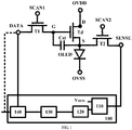
- FIG. 1 shows a schematic diagram of an example of an OLED pixel circuit.
- the OLED pixel circuit includes a first transistor T1, a drive transistor Td, a second transistor T2, a capacitor Cst, and a light emitting device OLED and a sensing element 100.
- a control electrode of the first transistor T1 is coupled to a first scan signal terminal SCAN1
- a first electrode of the first transistor T1 is coupled to a data signal terminal DATA
- a second electrode of the first transistor T1 is coupled to a control electrode of the drive transistor Td.
- a first electrode of the drive transistor Td is coupled to a first power supply OVDD
- a second electrode of the drive transistor Td is coupled to an anode of the light emitting device OLED.
- a control electrode of the second transistor T2 is coupled to a second scan signal terminal SCAN2, a first electrode of the second transistor T2 is coupled to a sense signal terminal SENSE, and a second electrode of the second transistor T2 is coupled to a second electrode of the drive transistor Td.
- a first terminal of the capacitor Cst is coupled to the control electrode of the drive transistor Td, and a second terminal of the capacitor Cst is coupled to the second electrode of the drive transistor Td.
- a cathode of the light emitting device OLED is coupled to a second power supply OVSS.
- the sensing element 100 is coupled to the data signal terminal DATA and the sense signal terminal SENSE.
- the sensing element 100 may include a port control circuit 110, a sensing circuit 120, a calculation circuit 130, and a voltage control circuit 140.
- the port control circuit 110 may control the state of the sense signal terminal SENSE to be in an output state or a floating state. In the output state, the sensing element 100 outputs a voltage V REFL through the sense signal terminal SENSE. In the floating state, the sensing element 100 may receive a current outputted from the second transistor T2 through the sense signal terminal SENSE.
- the sensing circuit 120 may detect the current received from the sense signal terminal SENSE.
- the calculation circuit 130 may calculate an external compensation voltage based on the sensed current.
- the voltage control circuit 140 is configured to add the external compensation voltage to the voltage of the data signal, as the voltage of the data signal.
- FIG. 1 merely schematically shows the sensing element 100.
- the port control circuit 110, the sensing circuit 120, the calculation circuit 130 and the voltage control circuit 140 in the sensing element 100 may be implemented by different devices, or may be integrated
- FIG. 2 is a timing diagram of each signal of the OLED pixel circuit as shown in FIG. 1 which is compensated in an external voltage compensation manner.
- the drive transistor Td is reset by enabling the first transistor T1 and the second transistor T2 so that a voltage at node S is V REFL (V REFL is, for example, 0V).
- V REFL is, for example, 0V
- the first transistor T1 is disabled and the second transistor T2 continues being enabled, so that the current flowing through the drive transistor Td is outputted to the sensing element 100 through the sense signal terminal SENSE.
- the voltage of the sense signal terminal SENSE gradually rises.
- the sensing charge is completed.
- the first transistor T1 and the second transistor T2 are enabled, and the voltage of the sense signal terminal SENSE is maintained at V SENSE .
- the sensing element calculates the voltage need to be compensated for adding the compensated voltage to the voltage of the data signal later on.
- the data signal terminal DATA the maximum value of the voltage of the data signal terminal DATA is schematically represented by VGm, and the minimum value of the voltage of the data signal terminal DATA is schematically represented by VG0.
- the data signals (Dn, Dn+1, ...) after compensation are used to drive the light emitting device OLED to emit light normally, which will not be described in detail herein.
- embodiments of the present disclosure provide a driving method for a pixel circuit.
- FIG. 3 is a schematic flowchart of a driving method for a pixel circuit according to an embodiment of the present disclosure.
- the drive transistor for driving the light emitting device in the OLED pixel circuit is compensated in a first compensation manner including an internal voltage compensation.
- the operation period of the light emitting device refers to a period during which the light emitting device is controlled to emit light, which may include a phase in which the light emitting device prepares to emit light and a phase in which the light emitting device emits light.
- the drive transistor is compensated in a second compensation manner including the internal voltage compensation and an external voltage compensation.
- the non-operation period of the light emitting device refers to a period during which the light emitting device is controlled not to emit light, for example, when the light-emitting device is in a phase during which the full screen is reset or when the light-emitting device is in a phase of an idle display between frames or rows.
- step S302 and step S304 are not limited. That is, step S304 may be performed before step S302.
- a small threshold voltage drift of the drive transistor may be compensated by an internal voltage compensation during an operation period of the light emitting device.
- the range of threshold voltage drift the internal voltage compensation can compensate is limited. After a long-term operation of the drive transistor, the threshold voltage drift gradually increases, and may exceed the range the internal voltage compensation can compensate.
- the drive transistor is compensated in a second compensation manner including the internal voltage compensation and the external voltage compensation, during a non-operation period of the light emitting device.
- the second compensation manner can compensate a greater threshold voltage drift by the external voltage compensation and achieve a better compensation accuracy by the internal voltage compensation.
- the driving method for the pixel circuit according to embodiments of the present disclosure does not affect the display effect negatively.
- the drive transistor may be compensated in the second compensation manner at time intervals. For instance, the compensation for the drive transistor in the second compensation manner is performed once, after the full screen is scanned each time.
- compensating the drive transistor in the OLED pixel circuit in the first compensation manner including an internal voltage compensation may include the following phases for example.
- a reset phase the drive transistor is reset.
- a compensation phase a voltage compensation is performed on the drive transistor.
- a data-in phase a data signal is inputted to the OLED pixel circuit.
- a light emitting phase the light emitting device is driven to emit light.
- compensating the drive transistor in a second compensation manner including the internal voltage compensation and the external voltage compensation may include the following phases for example.
- a reset phase the drive transistor is reset.
- a compensation phase a voltage compensation is performed on the drive transistor.
- a data signal is inputted to the OLED pixel circuit.
- a sensing phase a current flowing through the drive transistor is detected, and the external compensation voltage is calculated based on the current.
- the calculated external compensation voltage is used to compensate the voltage of the data signal.
- the external compensation voltage may be added to the voltage of the data signal, as the voltage of the data signal.
- the external compensation voltage refers to a threshold voltage value that needs to be compensated by an external device on the basis that the internal voltage compensation has compensated a portion of the drifted threshold voltage.
- the driving method for the pixel circuit according to embodiments of the present disclosure is not limited to be used for the OLED pixel circuit as shown in FIG. 1 . It should be understood by those skilled in the art that the driving method for the pixel circuit according to embodiments of the present disclosure may be used for any variation of the OLED pixel circuit as shown in FIG. 1 (e.g. in any embodiments including both an internal voltage compensation unit and an external voltage compensation unit).
- the range and accuracy of the threshold voltage shift of the drive transistor that can be compensated may be improved by the second compensation manner including the internal voltage compensation and the external voltage compensation, and thus requirement on the drift range of the threshold voltage of the drive transistor in an OLED pixel circuit may be relaxed. That is, even if the range of the threshold voltage shift of the drive transistor to be manufactured may moderately exceed the conventionally approved qualification range, the drive transistor may still be considered to be qualified, so that the yield of manufacturing the OLED pixel circuit can be improved.
- the internal voltage compensation performed in the second compensation manner can further avoid the hysteresis effect of the external voltage compensation and accelerate the sensing charging rate for the external voltage compensation.
- FIG. 4 shows a timing diagram of each signal of the OLED pixel circuit which is compensated in a first compensation manner according to an embodiment of the present disclosure.
- FIG. 5 shows an exemplary schematic diagram of the OLED pixel circuit when using the timing diagram as shown in FIG. 4 .
- the process of driving the OLED pixel circuit in the internal voltage compensation manner during the operation period of the light emitting device OLED in the OLED pixel circuit will be described below with reference to the OLED pixel circuit as shown in FIG. 4 .
- the process includes four phases: a reset phase, a compensation phase, a data-in phase, and a light emitting phase.
- the operation period of the light emitting device OLED refers to a period including the four phases above.
- a high voltage V H is inputted to the control electrode of the first transistor T1 (i.e., the first scan signal terminal SCAN1 is at the high voltage V H ) to enable the first transistor T1 so that the voltage of the control electrode (i.e., node G) of the drive transistor Td is equal to the first voltage V ref from the data signal terminal DATA.
- the high voltage V H is inputted to the control electrode of the second transistor T2 (i.e., the second scan signal terminal SCAN2 is at the high voltage V H ) to enable the second transistor T2 so that the voltage of the second electrode (i.e., node S) of the drive transistor Td is equal to the second voltage V L from the sense signal terminal SENSE.
- V L is set to be less than V ref (i.e., V L ⁇ V ref ).
- the first transistor T1 continues being enabled and the voltage of the data signal terminal DATA is maintained so that the voltage at node G is still V ref .
- a second voltage V L is inputted to the control electrode of the second transistor T2 (i.e., the second scan signal terminal SCAN2 is at the second voltage V L ) to disable the second transistor T2 so that the voltage of the second electrode (i.e., node S) of the drive transistor Td rises from the second voltage V L to a differential voltage between the first voltage V ref and a threshold voltage V th_t1 of the drive transistor Td (i.e., the voltage at node S is equal to V ref - V th_t1 ).
- the differential voltage between voltages of node G and node S is the threshold voltage V th_t1 of the drive transistor Td.
- the voltage at the data signal terminal DATA is changed into the third voltage V DATA .
- the first transistor T1 continues being enabled.
- the voltage at node G is raised to V DATA by the voltage V DATA of the data signal from the data signal terminal DATA to enable the drive transistor Td.
- the second transistor T2 continues being disabled so that the voltage at the second electrode (i.e., node S) of the drive transistor Td continues rising. And the capacitor Cst is charged in this phase.
- FIG. 6 shows a schematic diagram of voltage change at node S in this phase.
- the voltage at node S gradually rises. For instance, at time t1, the voltage at node S rises by ⁇ V. Finally, the voltage at node S will reach an upper limit value V DATA -V th_t1 and maintain this voltage value.
- the voltage at node S is V ref -V th_t1 + ⁇ V.
- the first transistor T1 is disabled and the second transistor T2 continues being disabled.
- the drive transistor Td continues being enabled with the holding function of the capacitor Cst.
- the voltage at node S is raised by the high voltage from the first power supply OVDD so as to cause the light emitting device OLED to emit light.
- the current flow direction in the OLED pixel circuit in this phase is shown by an arrow in FIG. 5 .
- the voltage at node S is eventually raised to the sum (i.e., to OVSS+V OLED ) of the second power supply voltage OVSS and the light emitting voltage V OLED of the light emitting device OLED.
- ⁇ n represents a carrier mobility of the drive transistor Td
- C ox represents a gate oxide layer capacitance
- W L represents a width-length ratio of the drive transistor Td.
- ⁇ V is positively correlated with ⁇ n
- ⁇ V can be controlled by controlling the duration of inputting a data signal to the OLED pixel circuit, so as to compensate the carrier mobility ⁇ n of the drive transistor Td, thereby stabilizing the current I OLED .
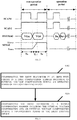
- FIG. 7 is a timing diagram of each signal of the OLED pixel circuit which is compensated in a second compensation manner according to an embodiment of the present disclosure.
- FIG. 8 is an exemplary schematic diagram of the OLED pixel circuit when using the timing diagram as shown in FIG. 7 .
- the process of driving the OLED pixel circuit in an manner including the internal voltage compensation and the external voltage compensation during the non-operation period of the light emitting device OLED in the OLED pixel circuit will be described below with reference to the OLED pixel circuit as shown in FIG. 8 .
- the process includes four phases: a reset phase, a compensation phase, a data-in phase, and a sensing phase.
- the high voltage V H is inputted to the control electrode of the first transistor T1 (i.e., the first scan signal terminal SCAN1 is at the high voltage V H ) to enable the first transistor T1 so that the voltage of the control electrode (i.e., node G) of the drive transistor Td is equal to the first voltage V ref from the data signal terminal DATA.
- the high voltage V H is inputted to the control electrode of the second transistor T2 (i.e., the second scan signal terminal SCAN2 is at the high voltage V H ) to enable the second transistor T2 so that the voltage of the second electrode (i.e., node S) of the drive transistor Td is equal to the second voltage V L from the sense signal terminal SENSE.
- V L is set to be less than V ref (i.e., V L ⁇ V ref ).
- the first transistor T1 continues being enabled and the voltage of the data signal terminal DATA is maintained so that the voltage at node G is still V ref .
- a second voltage V L is inputted to the control electrode of the second transistor T2 (i.e., the second scan signal terminal SCAN2 is at the second voltage V L ) to disable the second transistor T2 so that the voltage of the second electrode (i.e., node S) of the drive transistor Td rises from the second voltage V L to a differential voltage between the first voltage V ref and a threshold voltage V th_t1 of the drive transistor Td (i.e., the voltage at node S is equal to V ref - V th_t1 ).
- the differential voltage between voltages of node G and node S is the threshold voltage V th_t1 of the drive transistor Td.
- the voltage at the data signal terminal DATA is changed into the third voltage V DATA .
- the first transistor T1 continues being enabled.
- the voltage at node G is raised to V DATA by the voltage V DATA of the data signal from the data signal terminal DATA to enable the drive transistor Td.
- the second transistor T2 continues being disabled so that the voltage at the second electrode (i.e., node S) of the drive transistor Td continues rising. And the capacitor Cst is charged in this phase.
- the voltage at node S rises to V ref -V th_t1 + ⁇ V.
- V GS V DATA -(V ref -V th_t1 + ⁇ V).
- the first transistor T1 is disabled and the second transistor T2 is enabled.
- the drive transistor Td continues being enabled with the holding function of the capacitor Cst.
- the voltage at node S is raised by the high voltage from the first power supply OVDD, and the sense signal terminal SENSE is set to a floating state by controlling the sensing element connected to the sense signal terminal SENSE. Therefore, the current flowing through the drive transistor Td will not flow to the light emitting device OLED but will flow to the sensing element through the sense signal terminal SENSE.
- the direction of current flow in the OLED pixel circuit in this phase is shown by an arrow in FIG. 8 .
- the sensing element calculates the external compensation voltage based on the current, and adds the external compensation voltage to the voltage of the data signal, as the voltage of the data signal. Since the initial value (V ref -V th_t1 + ⁇ V) of the voltage at node S in the sensing phase is higher than the first voltage V ref , the sensing charging rate in the sensing phase of the present embodiment is greater than that in the case of starting sensing charging from V ref as shown in FIG. 2 ,. Furthermore, since the internal voltage compensation is performed first in the second compensation manner, the hysteresis effect of the external voltage compensation can be avoided.
- the driving method for a pixel circuit in the first and second compensation manners, the threshold voltage shift of the drive transistor can be compensated, the yield rate of the OLED pixel circuit is improved, the hysteresis effect of the external voltage compensation is avoided, and the sensing charging rate for the external voltage compensation is accelerated.
- the driving method for a pixel circuit according to embodiments of the present disclosure can also compensate the mobility of the drive transistor.
- the display apparatus may be used in any product having a display function, such as an electronic paper display, a mobile phone, a tablet computer, a TV set, a notebook computer, a digital photo frame, a wearable device or a navigation apparatus, and so on.
- a display function such as an electronic paper display, a mobile phone, a tablet computer, a TV set, a notebook computer, a digital photo frame, a wearable device or a navigation apparatus, and so on.
Landscapes
- Engineering & Computer Science (AREA)
- Physics & Mathematics (AREA)
- Computer Hardware Design (AREA)
- General Physics & Mathematics (AREA)
- Theoretical Computer Science (AREA)
- Control Of Indicators Other Than Cathode Ray Tubes (AREA)
- Control Of El Displays (AREA)
- Electroluminescent Light Sources (AREA)
Applications Claiming Priority (2)
| Application Number | Priority Date | Filing Date | Title |
|---|---|---|---|
| CN201710310558.3A CN108806599B (zh) | 2017-05-05 | 2017-05-05 | 用于补偿oled像素电路的方法 |
| PCT/CN2017/116383 WO2018201732A1 (fr) | 2017-05-05 | 2017-12-15 | Procédé d'attaque de circuit de pixels |
Publications (2)
| Publication Number | Publication Date |
|---|---|
| EP3621060A1 true EP3621060A1 (fr) | 2020-03-11 |
| EP3621060A4 EP3621060A4 (fr) | 2020-10-21 |
Family
ID=64016444
Family Applications (1)
| Application Number | Title | Priority Date | Filing Date |
|---|---|---|---|
| EP17899228.5A Pending EP3621060A4 (fr) | 2017-05-05 | 2017-12-15 | Procédé d'attaque de circuit de pixels |
Country Status (5)
| Country | Link |
|---|---|
| US (1) | US11087688B2 (fr) |
| EP (1) | EP3621060A4 (fr) |
| JP (1) | JP7084314B2 (fr) |
| CN (1) | CN108806599B (fr) |
| WO (1) | WO2018201732A1 (fr) |
Families Citing this family (16)
| Publication number | Priority date | Publication date | Assignee | Title |
|---|---|---|---|---|
| CN107863065A (zh) * | 2017-11-24 | 2018-03-30 | 京东方科技集团股份有限公司 | 像素单元电路、驱动方法和像素电路 |
| CN109166530B (zh) * | 2018-10-31 | 2020-04-14 | 合肥鑫晟光电科技有限公司 | 一种像素驱动电路的驱动方法及显示驱动电路、显示装置 |
| KR102626706B1 (ko) * | 2018-12-17 | 2024-01-17 | 엘지디스플레이 주식회사 | 기준전압의 왜곡이 방지된 유기전계발광 표시장치 |
| CN110047435B (zh) * | 2019-04-23 | 2020-12-04 | 京东方科技集团股份有限公司 | 像素驱动电路及其驱动方法、显示面板和显示装置 |
| CN110610682A (zh) * | 2019-08-20 | 2019-12-24 | 昆山国显光电有限公司 | 一种显示面板、像素电路的检测方法及显示装置 |
| CN110517641B (zh) * | 2019-08-30 | 2021-05-14 | 京东方科技集团股份有限公司 | 像素电路、参数检测方法、显示面板和显示装置 |
| CN110544456B (zh) * | 2019-09-05 | 2021-01-01 | 合肥京东方卓印科技有限公司 | 显示面板及其驱动方法、显示装置 |
| CN111415631B (zh) * | 2020-04-28 | 2022-07-12 | Tcl华星光电技术有限公司 | 背光模组和显示设备 |
| KR102834103B1 (ko) | 2020-10-26 | 2025-07-16 | 삼성디스플레이 주식회사 | 화소 회로, 이를 포함하는 표시 장치 및 화소 회로의 구동 방법 |
| US11170719B1 (en) * | 2020-12-10 | 2021-11-09 | Sharp Kabushiki Kaisha | TFT pixel threshold voltage compensation circuit with a source follower |
| CN116798326A (zh) * | 2022-03-14 | 2023-09-22 | 睿生光电股份有限公司 | 检测装置及检测装置的驱动方法 |
| CN114743516B (zh) * | 2022-04-11 | 2023-10-20 | 惠科股份有限公司 | 补偿电路及液晶显示设备 |
| CN114863892A (zh) * | 2022-05-12 | 2022-08-05 | 海宁奕斯伟集成电路设计有限公司 | 防静电干扰装置、方法及屏幕逻辑板 |
| CN114822406B (zh) * | 2022-05-20 | 2023-12-05 | 昆山国显光电有限公司 | 显示装置及其驱动方法 |
| CN115641804B (zh) * | 2022-10-31 | 2025-08-26 | 合肥京东方卓印科技有限公司 | 显示面板及其驱动方法、以及显示装置 |
| US12562089B2 (en) * | 2023-01-31 | 2026-02-24 | Chengdu Boe Optoelectronics Technology Co., Ltd. | Pixel driving circuit and method for driving same, display panel, and display device |
Family Cites Families (15)
| Publication number | Priority date | Publication date | Assignee | Title |
|---|---|---|---|---|
| JP4640449B2 (ja) * | 2008-06-02 | 2011-03-02 | ソニー株式会社 | 表示装置及びその駆動方法と電子機器 |
| KR101719481B1 (ko) * | 2010-10-26 | 2017-03-27 | 엘지디스플레이 주식회사 | 유기 발광장치 및 구동방법 |
| US9530349B2 (en) * | 2011-05-20 | 2016-12-27 | Ignis Innovations Inc. | Charged-based compensation and parameter extraction in AMOLED displays |
| CN103236237B (zh) * | 2013-04-26 | 2015-04-08 | 京东方科技集团股份有限公司 | 一种像素单元电路及其补偿方法、以及显示装置 |
| CN203179479U (zh) * | 2013-04-26 | 2013-09-04 | 京东方科技集团股份有限公司 | 一种像素单元电路以及显示装置 |
| CN105096817B (zh) * | 2014-05-27 | 2017-07-28 | 北京大学深圳研究生院 | 像素电路及其驱动方法和一种显示装置 |
| CN105280136B (zh) * | 2014-07-10 | 2018-11-30 | 信利半导体有限公司 | 一种amoled像素电路及其驱动方法 |
| CN104464621B (zh) * | 2014-11-14 | 2017-01-25 | 深圳市华星光电技术有限公司 | 补偿amoled电源压降的方法 |
| CN104658485B (zh) * | 2015-03-24 | 2017-03-29 | 京东方科技集团股份有限公司 | Oled驱动补偿电路及其驱动方法 |
| CN104700776B (zh) * | 2015-03-25 | 2016-12-07 | 京东方科技集团股份有限公司 | 像素电路及其驱动方法、显示装置 |
| CN104933993B (zh) * | 2015-07-17 | 2017-12-08 | 合肥鑫晟光电科技有限公司 | 像素驱动电路及其驱动方法、显示装置 |
| CN105161051A (zh) * | 2015-08-21 | 2015-12-16 | 京东方科技集团股份有限公司 | 像素电路及其驱动方法、阵列基板、显示面板及显示装置 |
| CN105976761B (zh) * | 2016-07-22 | 2018-05-11 | 京东方科技集团股份有限公司 | 一种像素驱动方法及显示面板 |
| CN106328061B (zh) * | 2016-10-14 | 2019-03-12 | 深圳市华星光电技术有限公司 | Oled像素混合补偿电路及混合补偿方法 |
| CN106409225B (zh) | 2016-12-09 | 2019-03-01 | 上海天马有机发光显示技术有限公司 | 有机发光像素补偿电路、有机发光显示面板及驱动方法 |
-
2017
- 2017-05-05 CN CN201710310558.3A patent/CN108806599B/zh active Active
- 2017-12-15 US US15/779,789 patent/US11087688B2/en active Active
- 2017-12-15 WO PCT/CN2017/116383 patent/WO2018201732A1/fr not_active Ceased
- 2017-12-15 EP EP17899228.5A patent/EP3621060A4/fr active Pending
- 2017-12-15 JP JP2018548885A patent/JP7084314B2/ja active Active
Also Published As
| Publication number | Publication date |
|---|---|
| JP7084314B2 (ja) | 2022-06-14 |
| US20200035159A1 (en) | 2020-01-30 |
| EP3621060A4 (fr) | 2020-10-21 |
| CN108806599A (zh) | 2018-11-13 |
| US11087688B2 (en) | 2021-08-10 |
| CN108806599B (zh) | 2020-01-14 |
| WO2018201732A1 (fr) | 2018-11-08 |
| JP2020518840A (ja) | 2020-06-25 |
Similar Documents
| Publication | Publication Date | Title |
|---|---|---|
| US11087688B2 (en) | Compensating method for pixel circuit | |
| US9589505B2 (en) | OLED pixel circuit, driving method of the same, and display device | |
| US11341908B2 (en) | Pixel circuit and driving method thereof, display panel and display device | |
| US10304380B2 (en) | Organic light-emitting pixel driving circuit, driving method, and organic light-emitting display panel | |
| US20200184893A1 (en) | Pixel circuit, drive method, electroluminescent light emitting display panel, and display apparatus | |
| US10909925B2 (en) | Pixel circuit and driving method thereof, display panel and display device | |
| US10297195B2 (en) | Pixel circuit and driving method thereof, array substrate, display panel and display device | |
| US9734763B2 (en) | Pixel circuit, driving method and display apparatus | |
| US10629127B2 (en) | Driving method of display device and display device | |
| US20180240400A1 (en) | Method for driving pixel circuit | |
| US9805654B2 (en) | Pixel circuit and its driving method, organic light-emitting display panel and display device | |
| US10770000B2 (en) | Pixel circuit, driving method, display panel and display device | |
| US20210082348A1 (en) | Amoled pixel driving circuit, driving method and terminal | |
| EP3048604B1 (fr) | Circuit d'excitation de pixels, procédé d'excitation de pixels et dispositif d'affichage | |
| US20160035276A1 (en) | Oled pixel circuit, driving method of the same, and display device | |
| US9412302B2 (en) | Pixel driving circuit, driving method, array substrate and display apparatus | |
| US9905166B2 (en) | Pixel driving circuit, pixel driving method and display apparatus | |
| US10515590B2 (en) | Pixel compensation circuit, driving method, display panel and display device | |
| US20190272785A1 (en) | Pixel circuit and drive method thereof, and display panel and display device | |
| CN111179850A (zh) | 像素补偿电路、阵列基板及显示面板 | |
| US11056063B2 (en) | Pixel circuit and driving method therefor, and display device | |
| US10140922B2 (en) | Pixel driving circuit and driving method thereof and display device | |
| US20180247592A1 (en) | Pixel Driving Circuit and Driving Method Thereof, Array Substrate, and Display Device | |
| US20180096654A1 (en) | Pixel circuit, display panel and display device | |
| US20190347993A1 (en) | Pixel circuit, driving method thereof, display panel and display device |
Legal Events
| Date | Code | Title | Description |
|---|---|---|---|
| STAA | Information on the status of an ep patent application or granted ep patent |
Free format text: STATUS: UNKNOWN |
|
| STAA | Information on the status of an ep patent application or granted ep patent |
Free format text: STATUS: THE INTERNATIONAL PUBLICATION HAS BEEN MADE |
|
| PUAI | Public reference made under article 153(3) epc to a published international application that has entered the european phase |
Free format text: ORIGINAL CODE: 0009012 |
|
| STAA | Information on the status of an ep patent application or granted ep patent |
Free format text: STATUS: REQUEST FOR EXAMINATION WAS MADE |
|
| 17P | Request for examination filed |
Effective date: 20180912 |
|
| AK | Designated contracting states |
Kind code of ref document: A1 Designated state(s): AL AT BE BG CH CY CZ DE DK EE ES FI FR GB GR HR HU IE IS IT LI LT LU LV MC MK MT NL NO PL PT RO RS SE SI SK SM TR |
|
| AX | Request for extension of the european patent |
Extension state: BA ME |
|
| DAV | Request for validation of the european patent (deleted) | ||
| DAX | Request for extension of the european patent (deleted) | ||
| A4 | Supplementary search report drawn up and despatched |
Effective date: 20200918 |
|
| RIC1 | Information provided on ipc code assigned before grant |
Ipc: G09G 3/3208 20160101ALI20200914BHEP Ipc: G09G 3/3258 20160101AFI20200914BHEP |
|
| STAA | Information on the status of an ep patent application or granted ep patent |
Free format text: STATUS: EXAMINATION IS IN PROGRESS |
|
| 17Q | First examination report despatched |
Effective date: 20221028 |