EP3621078B1 - Mémoire non volatile basée sur des transistors à effet de champ ferroélectriques - Google Patents
Mémoire non volatile basée sur des transistors à effet de champ ferroélectriques Download PDFInfo
- Publication number
- EP3621078B1 EP3621078B1 EP18193488.6A EP18193488A EP3621078B1 EP 3621078 B1 EP3621078 B1 EP 3621078B1 EP 18193488 A EP18193488 A EP 18193488A EP 3621078 B1 EP3621078 B1 EP 3621078B1
- Authority
- EP
- European Patent Office
- Prior art keywords
- write
- voltage
- applying
- transistor
- gate
- Prior art date
- Legal status (The legal status is an assumption and is not a legal conclusion. Google has not performed a legal analysis and makes no representation as to the accuracy of the status listed.)
- Active
Links
Images


Classifications
-
- H—ELECTRICITY
- H10—SEMICONDUCTOR DEVICES; ELECTRIC SOLID-STATE DEVICES NOT OTHERWISE PROVIDED FOR
- H10B—ELECTRONIC MEMORY DEVICES
- H10B51/00—Ferroelectric RAM [FeRAM] devices comprising ferroelectric memory transistors
- H10B51/30—Ferroelectric RAM [FeRAM] devices comprising ferroelectric memory transistors characterised by the memory core region
-
- G—PHYSICS
- G11—INFORMATION STORAGE
- G11C—STATIC STORES
- G11C11/00—Digital stores characterised by the use of particular electric or magnetic storage elements; Storage elements therefor
- G11C11/21—Digital stores characterised by the use of particular electric or magnetic storage elements; Storage elements therefor using electric elements
- G11C11/22—Digital stores characterised by the use of particular electric or magnetic storage elements; Storage elements therefor using electric elements using ferroelectric elements
- G11C11/225—Auxiliary circuits
- G11C11/2275—Writing or programming circuits or methods
-
- G—PHYSICS
- G11—INFORMATION STORAGE
- G11C—STATIC STORES
- G11C11/00—Digital stores characterised by the use of particular electric or magnetic storage elements; Storage elements therefor
- G11C11/21—Digital stores characterised by the use of particular electric or magnetic storage elements; Storage elements therefor using electric elements
- G11C11/22—Digital stores characterised by the use of particular electric or magnetic storage elements; Storage elements therefor using electric elements using ferroelectric elements
- G11C11/223—Digital stores characterised by the use of particular electric or magnetic storage elements; Storage elements therefor using electric elements using ferroelectric elements using MOS with ferroelectric gate insulating film
-
- G—PHYSICS
- G11—INFORMATION STORAGE
- G11C—STATIC STORES
- G11C11/00—Digital stores characterised by the use of particular electric or magnetic storage elements; Storage elements therefor
- G11C11/21—Digital stores characterised by the use of particular electric or magnetic storage elements; Storage elements therefor using electric elements
- G11C11/22—Digital stores characterised by the use of particular electric or magnetic storage elements; Storage elements therefor using electric elements using ferroelectric elements
- G11C11/225—Auxiliary circuits
- G11C11/2259—Cell access
-
- G—PHYSICS
- G11—INFORMATION STORAGE
- G11C—STATIC STORES
- G11C11/00—Digital stores characterised by the use of particular electric or magnetic storage elements; Storage elements therefor
- G11C11/21—Digital stores characterised by the use of particular electric or magnetic storage elements; Storage elements therefor using electric elements
- G11C11/22—Digital stores characterised by the use of particular electric or magnetic storage elements; Storage elements therefor using electric elements using ferroelectric elements
- G11C11/225—Auxiliary circuits
- G11C11/2273—Reading or sensing circuits or methods
-
- G—PHYSICS
- G11—INFORMATION STORAGE
- G11C—STATIC STORES
- G11C11/00—Digital stores characterised by the use of particular electric or magnetic storage elements; Storage elements therefor
- G11C11/21—Digital stores characterised by the use of particular electric or magnetic storage elements; Storage elements therefor using electric elements
- G11C11/34—Digital stores characterised by the use of particular electric or magnetic storage elements; Storage elements therefor using electric elements using semiconductor devices
- G11C11/40—Digital stores characterised by the use of particular electric or magnetic storage elements; Storage elements therefor using electric elements using semiconductor devices using transistors
- G11C11/401—Digital stores characterised by the use of particular electric or magnetic storage elements; Storage elements therefor using electric elements using semiconductor devices using transistors forming cells needing refreshing or charge regeneration, i.e. dynamic cells
- G11C11/4063—Auxiliary circuits, e.g. for addressing, decoding, driving, writing, sensing or timing
- G11C11/407—Auxiliary circuits, e.g. for addressing, decoding, driving, writing, sensing or timing for memory cells of the field-effect type
- G11C11/409—Read-write [R-W] circuits
- G11C11/4096—Input/output [I/O] data management or control circuits, e.g. reading or writing circuits, I/O drivers or bit-line switches
-
- H—ELECTRICITY
- H10—SEMICONDUCTOR DEVICES; ELECTRIC SOLID-STATE DEVICES NOT OTHERWISE PROVIDED FOR
- H10B—ELECTRONIC MEMORY DEVICES
- H10B12/00—Dynamic random access memory [DRAM] devices
- H10B12/01—Manufacture or treatment
-
- H—ELECTRICITY
- H10—SEMICONDUCTOR DEVICES; ELECTRIC SOLID-STATE DEVICES NOT OTHERWISE PROVIDED FOR
- H10B—ELECTRONIC MEMORY DEVICES
- H10B12/00—Dynamic random access memory [DRAM] devices
- H10B12/50—Peripheral circuit region structures
-
- H—ELECTRICITY
- H10—SEMICONDUCTOR DEVICES; ELECTRIC SOLID-STATE DEVICES NOT OTHERWISE PROVIDED FOR
- H10B—ELECTRONIC MEMORY DEVICES
- H10B51/00—Ferroelectric RAM [FeRAM] devices comprising ferroelectric memory transistors
- H10B51/10—Ferroelectric RAM [FeRAM] devices comprising ferroelectric memory transistors characterised by the top-view layout
-
- H—ELECTRICITY
- H10—SEMICONDUCTOR DEVICES; ELECTRIC SOLID-STATE DEVICES NOT OTHERWISE PROVIDED FOR
- H10B—ELECTRONIC MEMORY DEVICES
- H10B51/00—Ferroelectric RAM [FeRAM] devices comprising ferroelectric memory transistors
- H10B51/40—Ferroelectric RAM [FeRAM] devices comprising ferroelectric memory transistors characterised by the peripheral circuit region
Definitions
- the present disclosure is directed, in general, to semiconductor memory and, more specifically, to an integrated circuit including a three transistor random access memory, 3T RAM, cell and a method of operating an integrated circuit including a 3T RAM cell.
- a typical computer memory is designed to store many thousands of bits of information. These bits are stored in individual memory cells that may be organized in a crossbar architecture to make efficient use of space on a semiconductor substrate containing the memory.
- the crossbar architecture includes an array of memory cells, a plurality of parallel word lines extended along columns (or rows) of the memory cells, and a plurality of parallel bit lines extended along rows (or columns) of the memory cells.
- a commonly used cell architecture is the six transistor static random access memory, 6T SRAM, cell.
- 6T SRAM six transistor static random access memory
- 3T DRAM three transistor dynamic random access memory
- U.S. Pat. No. 8,379,433 Another commonly used cell architecture is a three transistor dynamic random access memory, 3T DRAM, which has for example been disclosed in U.S. Pat. No. 8,379,433 .
- a drawback of each DRAM cell is that it requires periodic refreshing of its memory state.
- U.S. Pat. No. 5,737,261 describes a ferroelectric memory using residual polarization of a ferroelectric film.
- the memory includes a semiconductor substrate of one conductive type; a write transistor having a source region and a drain region of another conductive type formed at a surface of the semiconductor substrate; a read transistor having a source region and a drain region of another conductive type formed at the surface of the semiconductor substrate; and a storage transistor having a source region and a drain region of one conductive type at the surface of the semiconductor substrate.
- a non-volatile semiconductor memory device includes: a memory cell including an MOS transistor for reading, an MOS transistor for writing, and an MFS transistor provided with a gate having a ferroelectric film above a channel region, one of a drain and a source of the MFS transistor having a common electric potential; a bit line for writing, to which the gate of the MFS transistor is connected through the MOS transistor for writing, and to which multivalued data having at least three voltage levels or analog data is input; a bit line for reading, to which the other of the drain and the source of the MFS transistor is connected through the MOS transistor for reading, and from which multivalued data having at least three voltage levels or analog data is read; a word line for writing connected to a gate of the MOS transistor for writing; and a word line for reading connected to a gate of the MOS transistor for reading.
- It is an aim of the present disclosure is to provide an improved memory cell, which can for example be used in SRAM- or DRAM-like memories.
- a first aspect of the present disclosure provides an integrated circuit including at least one three transistor random access memory, 3T RAM, cell.
- the 3T RAM cell includes a first transistor having a first gate connected as a storage node and a second transistor connected between the first transistor and a read bit line having a second gate connected to a read word line.
- the 3T RAM cell also includes a third transistor connected between the storage node and a write bit line having a third gate connected to a write word line.
- the first transistor is a ferroelectric-based field effect transistor, FeFET.
- Ferroelectric FETs offer advantageous properties for low power nonvolatile memories by virtue of their three-terminal structure coupled with the ability of the ferroelectric material to retain its polarization in the absence of an electric field. Utilizing the distinct features of FeFETs, a 3T RAM FeFET-based nonvolatile memory cell is disclosed, preferably with separate read and write paths.
- the circuit may further comprise a memory controller adapted to apply a write scheme or read scheme to the at least one cell.
- the write scheme may comprise: applying a write voltage to the write word line and applying the write voltage or ground voltage to the write bit line
- the read scheme may comprise: applying a read voltage to the read word line and applying ground voltage to the write word line.
- the gate dielectric of the second transistor and the gate dielectric of the third transistor are gate oxides, wherein the gate oxide thickness of the third transistor is larger than the gate oxide thickness of the second transistor such that the third transistor is adapted to sustain a double gate electrical field relative to the second transistor.
- the third transistor is able to withstand a higher supply voltage.
- This embodiment may comprise a memory controller adapted to apply the following write scheme to the at least one cell: applying a write voltage to the write word line and applying the write voltage or the negative write voltage to the write bit line; and/or adapted to apply the following read scheme to the at least one cell: applying a read voltage to the read word line and the write word line and applying a further voltage ranging from ground voltage to the read voltage to the write bit line.
- the source of the first transistor is connected to a further bit line.
- This embodiment may comprise a memory controller adapted to apply the following write scheme to the at least one cell: applying a write voltage to the write word line, applying the write voltage to one of the group consisting of the write bit line and the further bit line and applying ground voltage to the other one of said group, and/or adapted to apply the following read scheme to the at least one cell: applying a read voltage to the read word line and the write word line, applying a further voltage ranging from ground voltage to the read voltage to the write bit line and applying ground voltage to the further bit line.
- a second aspect of the present disclosure relates to a method of manufacturing an integrated circuit including a three transistor dynamic random access memory, 3 T RAM, cell.
- the method includes the steps of: providing a substrate, dividing the substrate in at least three sections, e.g. by shallow trench isolation, forming at least one field effect transistor, FET, in each section, and back end of line, BEOL, processing, comprising the formation of a plurality of metal layers interconnected by conductive via structures and connected to the front end of line, FEOL.
- the substrate may be a bulk silicon, Si, wafer or a silicon-on-insulator, SOI, wafer, preferably a fully depleted silicon-on-insulator, FD-SOI.
- the formation of the FET comprising the substeps of: forming a source region and a drain region in the substrate separated by a channel region; and growth of a gate dielectric that is arranged in-between a gate and the channel region, in-between the gate and the source region, and in-between the gate and the drain region.
- a ferroelectric field effect transistor, FeFET is formed.
- Forming the at least one FET is performed such that a bit line is connected to the source of a first FeFET, and that the gate dielectric of a second FET and the gate dielectric of a third FET are gate oxides, wherein a gate oxide thickness of the third FET is larger than a gate oxide thickness of the second FET such that the third FET is adapted to sustain a double gate electrical field relative to the second FET.
- the gate dielectric of the FeFET is a ferroelectric dielectric. In another embodiment, the gate dielectric of the FeFET is conductively connected to a ferroelectric dielectric provided in at least one of the metal layers of the BEOL.
- the at least one field effect transistor is formed as a single-gate planar FET or a multiple-gate FET, such as FinFET or trigate transistor.
- a third aspect of the present disclosure relates to a method of operating an integrated circuit including a three transistor dynamic random access memory, 3T RAM, cell, the method comprising writing a memory state on a storage node of the 3T RAM cell employing a write bit line and a write word line and/or reading the memory state on the storage node employing a read bit line and a read word line.
- top, bottom, over, under and the like in the description and the claims are used for descriptive purposes and not necessarily for describing relative positions. The terms so used are interchangeable under appropriate circumstances and the embodiments of the disclosure described herein can operate in other orientations than described or illustrated herein.
- a device comprising A and B should not be limited to devices consisting only of components A and B, rather with respect to the present disclosure, the only enumerated components of the device are A and B, and further the claim should be interpreted as including equivalents of those components.
- Figure 1 illustrates a first embodiment of a planar single gate memory device (such as single gate bulk ferroelectric-Field Effect Transistor (ferro-FET), Partially Depleted-Semiconductor On Insulator (PD-SOI), Fully Depleted-Semiconductor On Insulator (FD-SOI)).
- the device comprises a substrate 110.
- the substrate 110 may be a bulk oxide structure, but the substrate may also be divided into layers, e.g. a lower oxide layer and a partly depleted silicon layer on top of the lower oxide layer.
- a source region 102 and a drain region 104 On a surface of the substrate 110 there is provided a source region 102 and a drain region 104.
- the source 102 and drain 104 are separated by a channel region 112.
- the material of the channel region may be a crystalline semiconductor material such as e.g. Si.
- a gate structure 108 Above the channel region 112, there is provided a gate structure 108.
- a dielectric structure 114, 106a, 106b arranged between the gate structure 108 and the channel region 114.
- the dielectric structure 114, 106a, 106b comprises a ferroelectric memory region 114, e.g. from a Hf-based ferroelectric material.
- an upper part of the channel region 112 may be narrowed towards the ferroelectric memory region 114. This may for example be achieved by means of doping, forming LDD/HDD junctions, such that an effective area of the channel region 112 (i.e.
- the area of an interface between the ferroelectric memory region 114 and the channel region 112) is reduced.
- a projection of the gate 108 on the surface portion of the substrate 110 overlaps with the source 102 and drain 104 regions and defines a first overlap region 118a with the source region, and a second overlap region 118b with the drain region.
- the gate structure defines a gate length 116, and wherein a combined length of the first 118a and second 118b overlap regions is at least 5% of the gate length 116.
- the combined area of the first 118a and second 118b overlap regions is larger than the area of an interface between the dielectric structure 114, 106a, 106b and the channel region 112.
- a ratio between a combined area of the first 118a and second 118b overlap regions and an area of an interface between the dielectric structure and the channel region (effective channel area) is adapted such that the ferroelectric memory region is programmable by an electric field applied between the gate structure and source and drain region through the ferroelectric region.
- the dielectric structures 106a, 106b are provided beside the gate structure 108 in a current flow direction of the channel 112.
- Such structures may also be called spacers.
- the dielectric structures 106a-b may be formed by a ferroelectric material. Consequently, the read window of the device may be increased.
- Figure 2 illustrates a second embodiment of a planar single gate memory device (such as single gate bulk ferro-FET, PD-SOI, FD-SOI), similar to the embodiment of figure 1 .
- the ferro-electric memory region is provided around the gate structure 108.
- the gate structure 108 has a second surface not facing the surface portion of the substrate 110, wherein the ferroelectric memory region 114 comprises an interface with said first and second surface.
- the ferroelectric memory region 114 is provided also laterally positioned to the gate structure 108.
- Figure 3 illustrates a third embodiment of a planar single gate memory device (such as single gate bulk ferro-FET, PD-SOI, FD-SOI), similar to the embodiment of figure 2 .
- the ferroelectric memory region 114 is provided also laterally positioned to the gate structure 108, like in figure 2 .
- the read window of the device is further increased by providing spacers 106a, 106b outside the ferroelectric memory region 114, laterally positioned to the gate structure 108.
- Figure 4 illustrates a fourth embodiment of a planar single gate memory device (such as single gate bulk ferro-FET, PD-SOI, FD-SOI), similar to the embodiment of figure 3 .
- a region between the gate 108 and the effective channel area comprises a non-ferroelectric high-k material 116, to provide a further increased read window for the device.
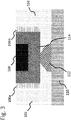
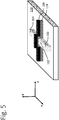
- FIG 5 shows schematically a FinFET formed on a substrate 110 wherein source 102 and drain 104 regions are formed in a semiconductor fin at opposite sides thereof in lateral direction along the y-axis.
- a gate structure 108 straddles the fin in a direction perpendicular to its lateral direction thereby separating the source 102 and drain 104 regions by a channel region 112 underneath the gate structure 108.
- the gate structure 108 and the channel region 112 are separated by a dielectric structure 114, in this case a ferroelectric memory region 114.
- the gate structure 108 defines a first overlap region with the source region 102, and a second overlap region with the drain region 104.
- the gate structure 108 defines a gate length 116, and a combined length of the first and second overlap regions is at least 5% of the gate length 116. According to some embodiments, the combined area of the first and second overlap regions is larger than the area of an interface between the dielectric structure 114 and the channel region 112 (i.e. the effective channel area).
- Figure 6 illustrates a first embodiment of a multigate device, which is similar to the device of figure 5 .
- the spacers 106a, 106b are provided beside the gate structure 108 in a current flow direction of the channel 112, like in figure 1 .
- Figure 7 illustrates a second embodiment of a multigate device, which is similar to the device of figure 6 .
- the ferroelectric memory region 114 is also provided laterally positioned to the gate structure 108 in a y-direction, like in figure 3 .
- spacers 106a, 106b are provided outside the ferroelectric memory region 114, laterally positioned to the gate structure 108.
- the concept may further be provided for a gate-all-around FeFET memory device.
- the gate structure arranged to at least partly enclose the channel region (thus being substantially pipe shaped), wherein the dielectric structure is formed on an inside surface of the gate structure.
- the channel is thus extending through the gate structure.
- the gate structure further at least partly enclose at least parts of the source region and the drain region.
- programming of the FeFET memory device can be achieved by a method for programming a FeFET memory device as described herein, the method comprising:
- the method of programming the device may comprise the step of achieving the first voltage difference by providing a supply voltage to the gate and a ground to the source and drain.
- the method of programming the device may comprise the step of achieving the second voltage difference by providing a supply voltage to the source and drain and a ground to the gate.
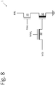
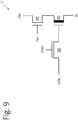
- FIGS 8 and 9 illustrate embodiments of three transistor random access memory, 3T RAM, cells generally designated 1,1' and constructed according to the principles of the present disclosure.
- the 3T RAM cells 1,1' employ a read word line, RWL, and a write word line, WWL, structure.
- the 3T RAM cells 1, 1' may be included in an embedded memory connected to other portions of an integrated circuit.
- the 3T RAM cells 1,1' may be included in a discrete memory contained in the integrated circuit.
- the 3T RAM cell 1; 1' includes first and second transistors 10; 10', 20; 20' that are series-connected between a ground and a read bit line RBL, as shown.
- the first transistor 10; 10' is a ferroelectric field effect transistor, FeFET, that employs a gate as a storage node.
- the first transistor 10; 10' may be a FeFET memory device as disclosed in one of the figures 1-7 .
- the first transistor 10, 10' also employs a source connected to the ground, shown in figure 8 , or to a further bit line BL, shown in figure 9 , and a drain series-connected to a source of the second transistor 20; 20'.
- a drain of the second transistor 20; 20' is connected to the RBL, and a gate is employed as a second control element connected to a RWL.
- a third transistor 30; 30' is connected between the storage node and the WBL employing a drain and provides a gate as a second control element connected to a WWL 113.
- a source of the third transistor 30; 30' is employed to connect to the WBL, as shown.
- the read word line RWL activates the second transistor 20; 20' for the read operation by applying a read voltage V r
- the write word line WWL activates the third transistor 30; 30' by applying the read voltage V r ,.
- a write voltage V dd corresponding to a desired logic state for the 3T RAM cell 1 is placed on the WBL.
- the write word line WWL activates the third transistor 30; 30' for the write operation
- the write voltage corresponding to the desired logic state on the WBL is transferred to the gate of the first transistor 10, 10' thereby adjusting the storage node 10; 10' to the desired logic state for the 3T RAM cell 1.
- the read word line RWL is activated by applying a voltage equal to or larger than the voltage applied to the write word line WWL.
- a complimentary logic of the write bit line WBL may be transferred to the read bit line RBL and the further bit line BL during a write operation.
- Figures 10 and 11 illustrate embodiments of a partially-fabricated integrated circuit device constructed according to a method of manufacturing of the present disclosure.
- the method comprises front end of line, FEOL, processing of the device by providing a substrate 210, 210' which contains transistors divided by isolation 220, 220'.
- the substrate 210, 210' may be a bulk Si structure, but the substrate may also be divided into layers, e.g. a lower oxide layer and a fully depleted silicon layer on top of the lower oxide layer.
- the transistors may be a single-gate planar FET, shown in figures 1-4 , or a multiple-gate FET, shown in figures 5 , 6 and 7 , such as FinFET or trigate transistor.
- the FEOL processing comprises providing a substrate 210, 210', e.g. a bulk silicon, Si, wafer or a silicon-on-insulator, SOI, wafer, preferably a fully depleted silicon-on-insulator, FD-SOI, and dividing that substrate three sections, for example by shallow trench isolation.
- the FEOL processing further comprises, in each section, forming a source region 230, 230' and a drain region 240, 240' in the substrate separated by a channel region 250, 250' and growing a gate dielectric 260; 260'; 261 that is arranged in-between a gate and the channel region, in-between the gate and the source region, and in-between the gate and the drain region.
- the material of the channel region may be a crystalline semiconductor material such as e.g. Si.
- the method comprises back end of line, BEOL, processing of the device by formation of a plurality of metal layers 320, 320' interconnected by conductive via structures 310, 310' and connected to the front end of line.
- a ferroelectric dielectric is provided, either as the gate dielectric 261, shown in figure 10 , or provided in at least one of the metal layers 320, 320' of the BEOL, shown in figure 11 .
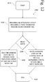
- FIG. 12 illustrates a flow diagram of an embodiment of a method 1000 of operating an integrated circuit including a three transistor random access memory, 3T RAM, cell constructed according to the principles of the present disclosure.
- the method 1200 starts in a step 1210, and the integrated circuit with the 3T RAM cell is provided in a step 1220.
- a step 1240 a memory state is written on a storage node of the 3T DRAM cell employing a write bit line and a write word line controlling a transistor connected to the write bit line.
- a memory state on the storage node is read employing a read bit line and a read word line controlling a transistor connected to the write bit line, in a step 1230.
- the method 1200 ends in a step 1250.
Landscapes
- Engineering & Computer Science (AREA)
- Computer Hardware Design (AREA)
- Databases & Information Systems (AREA)
- Microelectronics & Electronic Packaging (AREA)
- Manufacturing & Machinery (AREA)
- Semiconductor Memories (AREA)
Claims (15)
- Circuit intégré comprenant au moins une cellule de mémoire vive à trois transistors, RAM 3T, (1, 1'), comprenant :un premier transistor (10, 10') ayant une première grille connectée comme un nœud de stockage ;un deuxième transistor (20, 20') connecté entre le premier transistor et une ligne de bits de lecture (RBL) ayant une deuxième grille connectée à une ligne de mots de lecture (RWL) ;un troisième transistor (30, 30') connecté entre le nœud de stockage et une ligne de bits d'écriture (WBL) ayant une troisième grille connectée à une ligne de mots d'écriture (WWL) ; etune ligne de bits supplémentaire (BL) connectée à une source du premier transistor (10, 10'),dans lequel le premier transistor (10, 10') est un transistor à effet de champ ferroélectrique, FeFET,dans lequel un diélectrique de grille du deuxième transistor et un diélectrique de grille du troisième transistor sont des oxydes de grille,caractérisé en ce qu'une épaisseur d'oxyde de grille du troisième transistor est plus grande qu'une épaisseur d'oxyde de grille du deuxième transistor (20, 20') de telle sorte que le troisième transistor (30, 30') est conçu pour supporter un champ électrique de grille double par rapport au deuxième transistor (20, 20').
- Circuit intégré selon la revendication 1, comprenant en outre un dispositif de commande de mémoire conçu pour appliquer le schéma d'écriture suivant à l'au moins une cellule :appliquer une tension d'écriture (Vdd) à la ligne de mots d'écriture (WWL) ; etappliquer la tension d'écriture (Vdd) ou une tension de masse à la ligne de bits d'écriture (WBL) ; et/ou conçu pour appliquer le schéma de lecture suivant à l'au moins une cellule :appliquer une tension de lecture (Vr) à la ligne de mots de lecture (RWL) ; etappliquer une tension de masse à la ligne de mots d'écriture (WWL).
- Circuit intégré selon la revendication 1, comprenant en outre un dispositif de commande de mémoire conçu pour appliquer le schéma d'écriture suivant à l'au moins une cellule :appliquer une tension d'écriture (Vdd) à la ligne de mots d'écriture (WWL) ; etappliquer la tension d'écriture (Vdd) ou la tension d'écriture négative (-Vdd) à la ligne de bits d'écriture (WBL) ;et/ou conçu pour appliquer le schéma de lecture suivant à l'au moins une cellule :appliquer une tension de lecture (Vr) à la ligne de mots de lecture (RWL) et à la ligne de mots d'écriture (WWL) ; etappliquer une tension supplémentaire allant de la tension de masse à la tension de lecture (Vr) à la ligne de bits d'écriture (WBL).
- Circuit intégré selon la revendication 1, comprenant en outre un dispositif de commande de mémoire conçu pour appliquer le schéma d'écriture suivant à l'au moins une cellule :appliquer une tension d'écriture (Vdd) à la ligne de mots d'écriture (WWL) ;appliquer la tension d'écriture (Vdd) à l'une parmi le groupe consistant en la ligne de bits d'écriture (WBL) et la ligne de bits supplémentaire (BL) ; etappliquer une tension de masse à l'autre dudit groupe,et/ou conçu pour appliquer le schéma de lecture suivant à l'au moins une cellule :
appliquer une tension de lecture (Vr) à la ligne de mots de lecture (RWL) et à la ligne de mots d'écriture (WWL) ; appliquer une tension supplémentaire allant de la tension de masse à la tension de lecture (Vr) à la ligne de bits d'écriture, et appliquer une tension de masse à la ligne de bits supplémentaire (BL). - Procédé de fabrication d'un circuit intégré comprenant une cellule de mémoire vive à trois transistors, RAM 3T, selon la revendication 1, comprenant les étapes suivantes :fournir un substrat (210, 210') ;diviser le substrat (210, 210') en au moins trois sections, de préférence par isolation par tranchée peu profonde ;former au moins un transistor à effet de champ, FET, dans chaque section, comprenant les sous-étapes suivantes :
former une région de source (230, 230') et une région de drain (240, 240') dans le substrat (210, 210') séparées par une région de canal (250, 250') ; et faire croître un diélectrique de grille (260, 260') qui est disposé entre une grille et la région de canal, entre la grille et la région de source, et entre la grille et la région de drain, etréaliser un traitement d'extrémité arrière de ligne, BEOL, comprenant la formation d'une pluralité de couches métalliques (320, 320') interconnectées par des structures de trou de raccordement conducteur (310, 310') et connectées à l'extrémité avant de ligne, FEOL,dans lequel, dans au moins une section, un transistor à effet de champ ferroélectrique, FeFET, est formé,dans lequel la formation de l'au moins un FET est effectuée de telle sorte qu'une ligne de bits est connectée à la source d'un premier FeFET, et que le diélectrique de grille d'un deuxième FET et le diélectrique de grille d'un troisième FET sont des oxydes de grille,caractérisé par le fait qu'une épaisseur d'oxyde de grille du troisième FET est supérieure à une épaisseur d'oxyde de grille du deuxième FET de telle sorte que le troisième FET est conçu pour supporter un champ électrique de grille double par rapport au deuxième FET. - Procédé selon la revendication 5, dans lequel, dans l'au moins une section, le diélectrique de grille (260, 260') est un diélectrique ferroélectrique.
- Procédé selon la revendication 5, dans lequel, dans l'au moins une section, le diélectrique de grille (260, 260') est connecté à un diélectrique ferroélectrique prévu dans au moins l'une des couches métalliques (320, 320') de la BEOL.
- Procédé selon l'une quelconque des revendications précédentes 5 à 7, dans lequel le substrat (210, 210') est une tranche de silicium, Si, massif ou une tranche de silicium sur isolant, SOI, de préférence un silicium sur isolant totalement appauvri, FD-SOI.
- Procédé selon l'une quelconque des revendications précédentes 5 à 8, dans lequel l'au moins un transistor à effet de champ est formé comme un FET planaire à grille unique.
- Procédé selon l'une quelconque des revendications précédentes 5 à 8, dans lequel l'au moins un transistor à effet de champ est formé comme un FET à grilles multiples, tel qu'un FinFET ou un transistor à triple grille.
- Procédé de fonctionnement d'un circuit intégré comprenant une cellule de mémoire vive à trois transistors, RAM 3T, comprenant :un transistor à effet de champ ferroélectrique (10, 10'), FeFET, ayant une première grille connectée comme un nœud de stockage ;un deuxième transistor (20, 20') connecté entre le premier transistor et une ligne de bits de lecture (RBL) ayant une deuxième grille connectée à une ligne de mots de lecture (RWL) ;un troisième transistor (30, 30') connecté entre le nœud de stockage et une ligne de bits d'écriture (WBL) ayant une troisième grille connectée à une ligne de mots d'écriture (WWL) ; etune ligne de bits supplémentaire (BL) connectée à une source du FeFET (10, 10'),ledit procédé comprenant les étapes suivantes :écrire un état de mémoire sur le nœud de stockage de la cellule de RAM 3T en utilisant la ligne de bits d'écriture et la ligne de mots d'écriture ; oulire l'état de mémoire sur le nœud de stockage en utilisant la ligne de bits de lecture et la ligne de mots de lecture,dans lequel un diélectrique de grille du deuxième transistor et un diélectrique de grille du troisième transistor sont des oxydes de grille,caractérisé par le fait qu'une épaisseur d'oxyde de grille du troisième transistor est plus grande qu'une épaisseur d'oxyde de grille du deuxième transistor (20, 20') de telle sorte que le troisième transistor (30, 30') est conçu pour supporter un champ électrique de grille double par rapport au deuxième transistor (20, 20').
- Procédé selon la revendication 11, comprenant l'étape d'écriture d'un état de mémoire sur un nœud de stockage d'une cellule de RAM 3T en utilisant une ligne de bits d'écriture et une ligne de mots d'écriture, par application de l'un des schémas d'écriture suivants à la cellule :appliquer une tension d'écriture (Vdd) à la ligne de mots d'écriture (WWL) ; etappliquer la tension d'écriture (Vdd) ou une tension de masse à la ligne de bits d'écriture (WBL),
OUappliquer une tension d'écriture (Vdd) à la ligne de mots d'écriture (WWL) ; etappliquer la tension d'écriture (Vdd) ou la tension d'écriture négative (-Vdd) à la ligne de bits d'écriture,
OUappliquer une tension d'écriture (Vdd) à la ligne de mots d'écriture (WWL) ;appliquer la tension d'écriture (Vdd) à l'une parmi le groupe consistant en la ligne de bits d'écriture (WBL) et la ligne de bits supplémentaire (BL) ; etappliquer une tension de masse à l'autre dudit groupe. - Procédé selon la revendication 11, comprenant l'étape de lecture de l'état de mémoire sur le nœud de stockage en utilisant la ligne de bits de lecture et la ligne de mots de lecture, par application de l'un des schémas de lecture suivants à la cellule :appliquer une tension de lecture (Vr) à la ligne de mots de lecture (RWL) ; etappliquer une tension de masse à la ligne de mots d'écriture (WWL),
OUappliquer une tension de lecture (Vr) à la ligne de mots de lecture et à la ligne de mots d'écriture ; etappliquer une tension supplémentaire allant de la tension de masse à la tension de lecture (Vr) à la ligne de bits d'écriture. - Procédé d'écriture d'un état de mémoire sur un nœud de stockage d'une cellule de RAM 3T selon l'une quelconque des revendications précédentes 11 à 13, en utilisant une ligne de bits d'écriture et une ligne de mots d'écriture, dans une architecture de mémoire matricielle, comprenant les étapes suivantes :appliquer une tension d'écriture (Vdd) à la ligne de mots d'écriture sélectionnée ;appliquer une tension d'écriture négative (-Vdd) aux lignes de mots d'écriture non sélectionnées ; etappliquer la tension d'écriture (Vdd) ou la tension d'écriture négative (-Vdd) à la ligne de bits d'écriture.
- Procédé de lecture d'un état de mémoire sur le nœud de stockage d'une cellule de RAM 3T selon l'une quelconque des revendications précédentes 11 à 13, en utilisant une ligne de bits de lecture et une ligne de mots de lecture ; etappliquer une tension de lecture (Vr) à la ligne de mots de lecture sélectionnée et à la ligne de mots d'écriture sélectionnée ;appliquer une tension de masse aux lignes de mots non sélectionnées ; etappliquer une tension d'écriture (Vdd), allant de la tension de masse à la tension de lecture (Vr), à la ligne de bits d'écriture.
Priority Applications (2)
| Application Number | Priority Date | Filing Date | Title |
|---|---|---|---|
| EP18193488.6A EP3621078B1 (fr) | 2018-09-10 | 2018-09-10 | Mémoire non volatile basée sur des transistors à effet de champ ferroélectriques |
| US16/565,112 US11211404B2 (en) | 2018-09-10 | 2019-09-09 | Memory devices based on ferroelectric field effect transistors |
Applications Claiming Priority (1)
| Application Number | Priority Date | Filing Date | Title |
|---|---|---|---|
| EP18193488.6A EP3621078B1 (fr) | 2018-09-10 | 2018-09-10 | Mémoire non volatile basée sur des transistors à effet de champ ferroélectriques |
Publications (2)
| Publication Number | Publication Date |
|---|---|
| EP3621078A1 EP3621078A1 (fr) | 2020-03-11 |
| EP3621078B1 true EP3621078B1 (fr) | 2021-10-27 |
Family
ID=63556221
Family Applications (1)
| Application Number | Title | Priority Date | Filing Date |
|---|---|---|---|
| EP18193488.6A Active EP3621078B1 (fr) | 2018-09-10 | 2018-09-10 | Mémoire non volatile basée sur des transistors à effet de champ ferroélectriques |
Country Status (2)
| Country | Link |
|---|---|
| US (1) | US11211404B2 (fr) |
| EP (1) | EP3621078B1 (fr) |
Families Citing this family (1)
| Publication number | Priority date | Publication date | Assignee | Title |
|---|---|---|---|---|
| CN119724267A (zh) * | 2023-09-28 | 2025-03-28 | 北京超弦存储器研究院 | 存储单元、存储器及其制备方法、电子设备 |
Family Cites Families (8)
| Publication number | Priority date | Publication date | Assignee | Title |
|---|---|---|---|---|
| JP2921812B2 (ja) * | 1992-12-24 | 1999-07-19 | シャープ株式会社 | 不揮発性半導体記憶装置 |
| JPH104148A (ja) * | 1996-06-18 | 1998-01-06 | Fujitsu Ltd | 強誘電体メモリ |
| CN102612714B (zh) * | 2009-11-13 | 2016-06-29 | 株式会社半导体能源研究所 | 半导体器件及其驱动方法 |
| US8379433B2 (en) | 2010-09-15 | 2013-02-19 | Texas Instruments Incorporated | 3T DRAM cell with added capacitance on storage node |
| US8796085B2 (en) * | 2012-10-12 | 2014-08-05 | Viktor Koldiaev | Vertical super-thin body semiconductor on dielectric wall devices and methods of their fabrication |
| US20160071947A1 (en) * | 2014-09-10 | 2016-03-10 | Globalfoundries Inc. | Method including a replacement of a dummy gate structure with a gate structure including a ferroelectric material |
| CN107533860B (zh) * | 2015-05-28 | 2022-02-08 | 英特尔公司 | 具有非易失性留存的基于铁电的存储器单元 |
| CN110574160B (zh) * | 2017-05-08 | 2023-05-19 | 美光科技公司 | 存储器阵列 |
-
2018
- 2018-09-10 EP EP18193488.6A patent/EP3621078B1/fr active Active
-
2019
- 2019-09-09 US US16/565,112 patent/US11211404B2/en active Active
Also Published As
| Publication number | Publication date |
|---|---|
| US20200083234A1 (en) | 2020-03-12 |
| EP3621078A1 (fr) | 2020-03-11 |
| US11211404B2 (en) | 2021-12-28 |
Similar Documents
| Publication | Publication Date | Title |
|---|---|---|
| US11348922B2 (en) | Memory cell comprising first and second transistors and methods of operating | |
| US11974425B2 (en) | Memory cell comprising first and second transistors and methods of operating | |
| US8077536B2 (en) | Method of operating semiconductor memory device with floating body transistor using silicon controlled rectifier principle | |
| US12230681B2 (en) | Semiconductor memory devices with different doping types | |
| TWI821065B (zh) | 包括電性浮體電晶體的記憶裝置 | |
| US12190941B2 (en) | Memory cell and memory device thereof | |
| US12250823B2 (en) | Non-volatile memory device and its operating method | |
| EP3621078B1 (fr) | Mémoire non volatile basée sur des transistors à effet de champ ferroélectriques | |
| US20250031380A1 (en) | 3t memory with enhanced speed of operation and data retention | |
| KR102959032B1 (ko) | 비휘발성 메모리 장치 및 이의 동작 방법 | |
| US20240243492A1 (en) | Memory Cell Comprising First and Second Transistors and Methods of Operating | |
| US20240107741A1 (en) | Memory Device Comprising an Electrically Floating Body Transistor | |
| KR20240095043A (ko) | 비휘발성 메모리 장치 및 이의 동작 방법 | |
| JPWO2023248418A5 (fr) |
Legal Events
| Date | Code | Title | Description |
|---|---|---|---|
| PUAI | Public reference made under article 153(3) epc to a published international application that has entered the european phase |
Free format text: ORIGINAL CODE: 0009012 |
|
| STAA | Information on the status of an ep patent application or granted ep patent |
Free format text: STATUS: THE APPLICATION HAS BEEN PUBLISHED |
|
| AK | Designated contracting states |
Kind code of ref document: A1 Designated state(s): AL AT BE BG CH CY CZ DE DK EE ES FI FR GB GR HR HU IE IS IT LI LT LU LV MC MK MT NL NO PL PT RO RS SE SI SK SM TR |
|
| AX | Request for extension of the european patent |
Extension state: BA ME |
|
| STAA | Information on the status of an ep patent application or granted ep patent |
Free format text: STATUS: REQUEST FOR EXAMINATION WAS MADE |
|
| 17P | Request for examination filed |
Effective date: 20200911 |
|
| RBV | Designated contracting states (corrected) |
Designated state(s): AL AT BE BG CH CY CZ DE DK EE ES FI FR GB GR HR HU IE IS IT LI LT LU LV MC MK MT NL NO PL PT RO RS SE SI SK SM TR |
|
| GRAP | Despatch of communication of intention to grant a patent |
Free format text: ORIGINAL CODE: EPIDOSNIGR1 |
|
| STAA | Information on the status of an ep patent application or granted ep patent |
Free format text: STATUS: GRANT OF PATENT IS INTENDED |
|
| INTG | Intention to grant announced |
Effective date: 20210507 |
|
| GRAS | Grant fee paid |
Free format text: ORIGINAL CODE: EPIDOSNIGR3 |
|
| GRAA | (expected) grant |
Free format text: ORIGINAL CODE: 0009210 |
|
| STAA | Information on the status of an ep patent application or granted ep patent |
Free format text: STATUS: THE PATENT HAS BEEN GRANTED |
|
| AK | Designated contracting states |
Kind code of ref document: B1 Designated state(s): AL AT BE BG CH CY CZ DE DK EE ES FI FR GB GR HR HU IE IS IT LI LT LU LV MC MK MT NL NO PL PT RO RS SE SI SK SM TR |
|
| REG | Reference to a national code |
Ref country code: GB Ref legal event code: FG4D |
|
| REG | Reference to a national code |
Ref country code: CH Ref legal event code: EP |
|
| REG | Reference to a national code |
Ref country code: AT Ref legal event code: REF Ref document number: 1442549 Country of ref document: AT Kind code of ref document: T Effective date: 20211115 |
|
| REG | Reference to a national code |
Ref country code: DE Ref legal event code: R096 Ref document number: 602018025592 Country of ref document: DE |
|
| REG | Reference to a national code |
Ref country code: IE Ref legal event code: FG4D |
|
| REG | Reference to a national code |
Ref country code: LT Ref legal event code: MG9D |
|
| REG | Reference to a national code |
Ref country code: NL Ref legal event code: MP Effective date: 20211027 |
|
| REG | Reference to a national code |
Ref country code: AT Ref legal event code: MK05 Ref document number: 1442549 Country of ref document: AT Kind code of ref document: T Effective date: 20211027 |
|
| PG25 | Lapsed in a contracting state [announced via postgrant information from national office to epo] |
Ref country code: RS Free format text: LAPSE BECAUSE OF FAILURE TO SUBMIT A TRANSLATION OF THE DESCRIPTION OR TO PAY THE FEE WITHIN THE PRESCRIBED TIME-LIMIT Effective date: 20211027 Ref country code: LT Free format text: LAPSE BECAUSE OF FAILURE TO SUBMIT A TRANSLATION OF THE DESCRIPTION OR TO PAY THE FEE WITHIN THE PRESCRIBED TIME-LIMIT Effective date: 20211027 Ref country code: FI Free format text: LAPSE BECAUSE OF FAILURE TO SUBMIT A TRANSLATION OF THE DESCRIPTION OR TO PAY THE FEE WITHIN THE PRESCRIBED TIME-LIMIT Effective date: 20211027 Ref country code: BG Free format text: LAPSE BECAUSE OF FAILURE TO SUBMIT A TRANSLATION OF THE DESCRIPTION OR TO PAY THE FEE WITHIN THE PRESCRIBED TIME-LIMIT Effective date: 20220127 Ref country code: AT Free format text: LAPSE BECAUSE OF FAILURE TO SUBMIT A TRANSLATION OF THE DESCRIPTION OR TO PAY THE FEE WITHIN THE PRESCRIBED TIME-LIMIT Effective date: 20211027 |
|
| PG25 | Lapsed in a contracting state [announced via postgrant information from national office to epo] |
Ref country code: IS Free format text: LAPSE BECAUSE OF FAILURE TO SUBMIT A TRANSLATION OF THE DESCRIPTION OR TO PAY THE FEE WITHIN THE PRESCRIBED TIME-LIMIT Effective date: 20220227 Ref country code: SE Free format text: LAPSE BECAUSE OF FAILURE TO SUBMIT A TRANSLATION OF THE DESCRIPTION OR TO PAY THE FEE WITHIN THE PRESCRIBED TIME-LIMIT Effective date: 20211027 Ref country code: PT Free format text: LAPSE BECAUSE OF FAILURE TO SUBMIT A TRANSLATION OF THE DESCRIPTION OR TO PAY THE FEE WITHIN THE PRESCRIBED TIME-LIMIT Effective date: 20220228 Ref country code: PL Free format text: LAPSE BECAUSE OF FAILURE TO SUBMIT A TRANSLATION OF THE DESCRIPTION OR TO PAY THE FEE WITHIN THE PRESCRIBED TIME-LIMIT Effective date: 20211027 Ref country code: NO Free format text: LAPSE BECAUSE OF FAILURE TO SUBMIT A TRANSLATION OF THE DESCRIPTION OR TO PAY THE FEE WITHIN THE PRESCRIBED TIME-LIMIT Effective date: 20220127 Ref country code: NL Free format text: LAPSE BECAUSE OF FAILURE TO SUBMIT A TRANSLATION OF THE DESCRIPTION OR TO PAY THE FEE WITHIN THE PRESCRIBED TIME-LIMIT Effective date: 20211027 Ref country code: LV Free format text: LAPSE BECAUSE OF FAILURE TO SUBMIT A TRANSLATION OF THE DESCRIPTION OR TO PAY THE FEE WITHIN THE PRESCRIBED TIME-LIMIT Effective date: 20211027 Ref country code: HR Free format text: LAPSE BECAUSE OF FAILURE TO SUBMIT A TRANSLATION OF THE DESCRIPTION OR TO PAY THE FEE WITHIN THE PRESCRIBED TIME-LIMIT Effective date: 20211027 Ref country code: GR Free format text: LAPSE BECAUSE OF FAILURE TO SUBMIT A TRANSLATION OF THE DESCRIPTION OR TO PAY THE FEE WITHIN THE PRESCRIBED TIME-LIMIT Effective date: 20220128 Ref country code: ES Free format text: LAPSE BECAUSE OF FAILURE TO SUBMIT A TRANSLATION OF THE DESCRIPTION OR TO PAY THE FEE WITHIN THE PRESCRIBED TIME-LIMIT Effective date: 20211027 |
|
| REG | Reference to a national code |
Ref country code: DE Ref legal event code: R097 Ref document number: 602018025592 Country of ref document: DE |
|
| PG25 | Lapsed in a contracting state [announced via postgrant information from national office to epo] |
Ref country code: SM Free format text: LAPSE BECAUSE OF FAILURE TO SUBMIT A TRANSLATION OF THE DESCRIPTION OR TO PAY THE FEE WITHIN THE PRESCRIBED TIME-LIMIT Effective date: 20211027 Ref country code: SK Free format text: LAPSE BECAUSE OF FAILURE TO SUBMIT A TRANSLATION OF THE DESCRIPTION OR TO PAY THE FEE WITHIN THE PRESCRIBED TIME-LIMIT Effective date: 20211027 Ref country code: RO Free format text: LAPSE BECAUSE OF FAILURE TO SUBMIT A TRANSLATION OF THE DESCRIPTION OR TO PAY THE FEE WITHIN THE PRESCRIBED TIME-LIMIT Effective date: 20211027 Ref country code: EE Free format text: LAPSE BECAUSE OF FAILURE TO SUBMIT A TRANSLATION OF THE DESCRIPTION OR TO PAY THE FEE WITHIN THE PRESCRIBED TIME-LIMIT Effective date: 20211027 Ref country code: DK Free format text: LAPSE BECAUSE OF FAILURE TO SUBMIT A TRANSLATION OF THE DESCRIPTION OR TO PAY THE FEE WITHIN THE PRESCRIBED TIME-LIMIT Effective date: 20211027 Ref country code: CZ Free format text: LAPSE BECAUSE OF FAILURE TO SUBMIT A TRANSLATION OF THE DESCRIPTION OR TO PAY THE FEE WITHIN THE PRESCRIBED TIME-LIMIT Effective date: 20211027 |
|
| PLBE | No opposition filed within time limit |
Free format text: ORIGINAL CODE: 0009261 |
|
| STAA | Information on the status of an ep patent application or granted ep patent |
Free format text: STATUS: NO OPPOSITION FILED WITHIN TIME LIMIT |
|
| 26N | No opposition filed |
Effective date: 20220728 |
|
| PG25 | Lapsed in a contracting state [announced via postgrant information from national office to epo] |
Ref country code: AL Free format text: LAPSE BECAUSE OF FAILURE TO SUBMIT A TRANSLATION OF THE DESCRIPTION OR TO PAY THE FEE WITHIN THE PRESCRIBED TIME-LIMIT Effective date: 20211027 |
|
| PG25 | Lapsed in a contracting state [announced via postgrant information from national office to epo] |
Ref country code: SI Free format text: LAPSE BECAUSE OF FAILURE TO SUBMIT A TRANSLATION OF THE DESCRIPTION OR TO PAY THE FEE WITHIN THE PRESCRIBED TIME-LIMIT Effective date: 20211027 |
|
| PG25 | Lapsed in a contracting state [announced via postgrant information from national office to epo] |
Ref country code: MC Free format text: LAPSE BECAUSE OF FAILURE TO SUBMIT A TRANSLATION OF THE DESCRIPTION OR TO PAY THE FEE WITHIN THE PRESCRIBED TIME-LIMIT Effective date: 20211027 |
|
| REG | Reference to a national code |
Ref country code: CH Ref legal event code: PL |
|
| GBPC | Gb: european patent ceased through non-payment of renewal fee |
Effective date: 20220910 |
|
| REG | Reference to a national code |
Ref country code: BE Ref legal event code: MM Effective date: 20220930 |
|
| PG25 | Lapsed in a contracting state [announced via postgrant information from national office to epo] |
Ref country code: IT Free format text: LAPSE BECAUSE OF FAILURE TO SUBMIT A TRANSLATION OF THE DESCRIPTION OR TO PAY THE FEE WITHIN THE PRESCRIBED TIME-LIMIT Effective date: 20211027 |
|
| P01 | Opt-out of the competence of the unified patent court (upc) registered |
Effective date: 20230513 |
|
| PG25 | Lapsed in a contracting state [announced via postgrant information from national office to epo] |
Ref country code: LU Free format text: LAPSE BECAUSE OF NON-PAYMENT OF DUE FEES Effective date: 20220910 |
|
| PG25 | Lapsed in a contracting state [announced via postgrant information from national office to epo] |
Ref country code: LI Free format text: LAPSE BECAUSE OF NON-PAYMENT OF DUE FEES Effective date: 20220930 Ref country code: IE Free format text: LAPSE BECAUSE OF NON-PAYMENT OF DUE FEES Effective date: 20220910 Ref country code: FR Free format text: LAPSE BECAUSE OF NON-PAYMENT OF DUE FEES Effective date: 20220930 Ref country code: CH Free format text: LAPSE BECAUSE OF NON-PAYMENT OF DUE FEES Effective date: 20220930 |
|
| PG25 | Lapsed in a contracting state [announced via postgrant information from national office to epo] |
Ref country code: BE Free format text: LAPSE BECAUSE OF NON-PAYMENT OF DUE FEES Effective date: 20220930 |
|
| PG25 | Lapsed in a contracting state [announced via postgrant information from national office to epo] |
Ref country code: GB Free format text: LAPSE BECAUSE OF NON-PAYMENT OF DUE FEES Effective date: 20220910 |
|
| PG25 | Lapsed in a contracting state [announced via postgrant information from national office to epo] |
Ref country code: HU Free format text: LAPSE BECAUSE OF FAILURE TO SUBMIT A TRANSLATION OF THE DESCRIPTION OR TO PAY THE FEE WITHIN THE PRESCRIBED TIME-LIMIT; INVALID AB INITIO Effective date: 20180910 |
|
| PG25 | Lapsed in a contracting state [announced via postgrant information from national office to epo] |
Ref country code: CY Free format text: LAPSE BECAUSE OF FAILURE TO SUBMIT A TRANSLATION OF THE DESCRIPTION OR TO PAY THE FEE WITHIN THE PRESCRIBED TIME-LIMIT Effective date: 20211027 |
|
| PG25 | Lapsed in a contracting state [announced via postgrant information from national office to epo] |
Ref country code: MK Free format text: LAPSE BECAUSE OF FAILURE TO SUBMIT A TRANSLATION OF THE DESCRIPTION OR TO PAY THE FEE WITHIN THE PRESCRIBED TIME-LIMIT Effective date: 20211027 |
|
| PG25 | Lapsed in a contracting state [announced via postgrant information from national office to epo] |
Ref country code: TR Free format text: LAPSE BECAUSE OF FAILURE TO SUBMIT A TRANSLATION OF THE DESCRIPTION OR TO PAY THE FEE WITHIN THE PRESCRIBED TIME-LIMIT Effective date: 20211027 |
|
| PG25 | Lapsed in a contracting state [announced via postgrant information from national office to epo] |
Ref country code: MT Free format text: LAPSE BECAUSE OF FAILURE TO SUBMIT A TRANSLATION OF THE DESCRIPTION OR TO PAY THE FEE WITHIN THE PRESCRIBED TIME-LIMIT Effective date: 20211027 |
|
| PGFP | Annual fee paid to national office [announced via postgrant information from national office to epo] |
Ref country code: DE Payment date: 20250820 Year of fee payment: 8 |