EP3621160A1 - Module de commande électronique et procédé de fabrication d'un module de commande électronique - Google Patents
Module de commande électronique et procédé de fabrication d'un module de commande électronique Download PDFInfo
- Publication number
- EP3621160A1 EP3621160A1 EP19181756.8A EP19181756A EP3621160A1 EP 3621160 A1 EP3621160 A1 EP 3621160A1 EP 19181756 A EP19181756 A EP 19181756A EP 3621160 A1 EP3621160 A1 EP 3621160A1
- Authority
- EP
- European Patent Office
- Prior art keywords
- circuit board
- printed circuit
- electronic component
- control module
- positioning pin
- Prior art date
- Legal status (The legal status is an assumption and is not a legal conclusion. Google has not performed a legal analysis and makes no representation as to the accuracy of the status listed.)
- Granted
Links
Images
Classifications
-
- H—ELECTRICITY
- H05—ELECTRIC TECHNIQUES NOT OTHERWISE PROVIDED FOR
- H05K—PRINTED CIRCUITS; CASINGS OR CONSTRUCTIONAL DETAILS OF ELECTRIC APPARATUS; MANUFACTURE OF ASSEMBLAGES OF ELECTRICAL COMPONENTS
- H05K3/00—Apparatus or processes for manufacturing printed circuits
- H05K3/30—Assembling printed circuits with electric components, e.g. with resistors
- H05K3/32—Assembling printed circuits with electric components, e.g. with resistors electrically connecting electric components or wires to printed circuits
- H05K3/325—Assembling printed circuits with electric components, e.g. with resistors electrically connecting electric components or wires to printed circuits by abutting or pinching; Mechanical auxiliary parts therefor
-
- H—ELECTRICITY
- H05—ELECTRIC TECHNIQUES NOT OTHERWISE PROVIDED FOR
- H05K—PRINTED CIRCUITS; CASINGS OR CONSTRUCTIONAL DETAILS OF ELECTRIC APPARATUS; MANUFACTURE OF ASSEMBLAGES OF ELECTRICAL COMPONENTS
- H05K3/00—Apparatus or processes for manufacturing printed circuits
- H05K3/30—Assembling printed circuits with electric components, e.g. with resistors
- H05K3/32—Assembling printed circuits with electric components, e.g. with resistors electrically connecting electric components or wires to printed circuits
- H05K3/34—Assembling printed circuits with electric components, e.g. with resistors electrically connecting electric components or wires to printed circuits by soldering
- H05K3/341—Surface mounted components
- H05K3/3421—Leaded components
-
- H—ELECTRICITY
- H01—ELECTRIC ELEMENTS
- H01R—ELECTRICALLY-CONDUCTIVE CONNECTIONS; STRUCTURAL ASSOCIATIONS OF A PLURALITY OF MUTUALLY-INSULATED ELECTRICAL CONNECTING ELEMENTS; COUPLING DEVICES; CURRENT COLLECTORS
- H01R12/00—Structural associations of a plurality of mutually-insulated electrical connecting elements, specially adapted for printed circuits, e.g. printed circuit boards [PCB], flat or ribbon cables, or like generally planar structures, e.g. terminal strips, terminal blocks; Coupling devices specially adapted for printed circuits, flat or ribbon cables, or like generally planar structures; Terminals specially adapted for contact with, or insertion into, printed circuits, flat or ribbon cables, or like generally planar structures
- H01R12/50—Fixed connections
- H01R12/51—Fixed connections for rigid printed circuits or like structures
- H01R12/55—Fixed connections for rigid printed circuits or like structures characterised by the terminals
- H01R12/57—Fixed connections for rigid printed circuits or like structures characterised by the terminals surface mounting terminals
-
- H—ELECTRICITY
- H01—ELECTRIC ELEMENTS
- H01R—ELECTRICALLY-CONDUCTIVE CONNECTIONS; STRUCTURAL ASSOCIATIONS OF A PLURALITY OF MUTUALLY-INSULATED ELECTRICAL CONNECTING ELEMENTS; COUPLING DEVICES; CURRENT COLLECTORS
- H01R12/00—Structural associations of a plurality of mutually-insulated electrical connecting elements, specially adapted for printed circuits, e.g. printed circuit boards [PCB], flat or ribbon cables, or like generally planar structures, e.g. terminal strips, terminal blocks; Coupling devices specially adapted for printed circuits, flat or ribbon cables, or like generally planar structures; Terminals specially adapted for contact with, or insertion into, printed circuits, flat or ribbon cables, or like generally planar structures
- H01R12/70—Coupling devices
- H01R12/7076—Coupling devices for connection between PCB and component, e.g. display
-
- H—ELECTRICITY
- H01—ELECTRIC ELEMENTS
- H01R—ELECTRICALLY-CONDUCTIVE CONNECTIONS; STRUCTURAL ASSOCIATIONS OF A PLURALITY OF MUTUALLY-INSULATED ELECTRICAL CONNECTING ELEMENTS; COUPLING DEVICES; CURRENT COLLECTORS
- H01R12/00—Structural associations of a plurality of mutually-insulated electrical connecting elements, specially adapted for printed circuits, e.g. printed circuit boards [PCB], flat or ribbon cables, or like generally planar structures, e.g. terminal strips, terminal blocks; Coupling devices specially adapted for printed circuits, flat or ribbon cables, or like generally planar structures; Terminals specially adapted for contact with, or insertion into, printed circuits, flat or ribbon cables, or like generally planar structures
- H01R12/70—Coupling devices
- H01R12/71—Coupling devices for rigid printing circuits or like structures
- H01R12/712—Coupling devices for rigid printing circuits or like structures co-operating with the surface of the printed circuit or with a coupling device exclusively provided on the surface of the printed circuit
- H01R12/716—Coupling device provided on the PCB
- H01R12/718—Contact members provided on the PCB without an insulating housing
-
- H—ELECTRICITY
- H01—ELECTRIC ELEMENTS
- H01R—ELECTRICALLY-CONDUCTIVE CONNECTIONS; STRUCTURAL ASSOCIATIONS OF A PLURALITY OF MUTUALLY-INSULATED ELECTRICAL CONNECTING ELEMENTS; COUPLING DEVICES; CURRENT COLLECTORS
- H01R13/00—Details of coupling devices of the kinds covered by groups H01R12/70 or H01R24/00 - H01R33/00
- H01R13/02—Contact members
- H01R13/22—Contacts for co-operating by abutting
- H01R13/24—Contacts for co-operating by abutting resilient; resiliently-mounted
- H01R13/2435—Contacts for co-operating by abutting resilient; resiliently-mounted with opposite contact points, e.g. C beam
-
- H—ELECTRICITY
- H01—ELECTRIC ELEMENTS
- H01R—ELECTRICALLY-CONDUCTIVE CONNECTIONS; STRUCTURAL ASSOCIATIONS OF A PLURALITY OF MUTUALLY-INSULATED ELECTRICAL CONNECTING ELEMENTS; COUPLING DEVICES; CURRENT COLLECTORS
- H01R43/00—Apparatus or processes specially adapted for manufacturing, assembling, maintaining, or repairing of line connectors or current collectors or for joining electric conductors
- H01R43/20—Apparatus or processes specially adapted for manufacturing, assembling, maintaining, or repairing of line connectors or current collectors or for joining electric conductors for assembling or disassembling contact members with insulating base, case or sleeve
- H01R43/205—Apparatus or processes specially adapted for manufacturing, assembling, maintaining, or repairing of line connectors or current collectors or for joining electric conductors for assembling or disassembling contact members with insulating base, case or sleeve with a panel or printed circuit board
-
- H—ELECTRICITY
- H05—ELECTRIC TECHNIQUES NOT OTHERWISE PROVIDED FOR
- H05K—PRINTED CIRCUITS; CASINGS OR CONSTRUCTIONAL DETAILS OF ELECTRIC APPARATUS; MANUFACTURE OF ASSEMBLAGES OF ELECTRICAL COMPONENTS
- H05K2201/00—Indexing scheme relating to printed circuits covered by H05K1/00
- H05K2201/03—Conductive materials
- H05K2201/0302—Properties and characteristics in general
- H05K2201/0311—Metallic part with specific elastic properties, e.g. bent piece of metal as electrical contact
-
- H—ELECTRICITY
- H05—ELECTRIC TECHNIQUES NOT OTHERWISE PROVIDED FOR
- H05K—PRINTED CIRCUITS; CASINGS OR CONSTRUCTIONAL DETAILS OF ELECTRIC APPARATUS; MANUFACTURE OF ASSEMBLAGES OF ELECTRICAL COMPONENTS
- H05K2201/00—Indexing scheme relating to printed circuits covered by H05K1/00
- H05K2201/09—Shape and layout
- H05K2201/09009—Substrate related
- H05K2201/09063—Holes or slots in insulating substrate not used for electrical connections
-
- H—ELECTRICITY
- H05—ELECTRIC TECHNIQUES NOT OTHERWISE PROVIDED FOR
- H05K—PRINTED CIRCUITS; CASINGS OR CONSTRUCTIONAL DETAILS OF ELECTRIC APPARATUS; MANUFACTURE OF ASSEMBLAGES OF ELECTRICAL COMPONENTS
- H05K2201/00—Indexing scheme relating to printed circuits covered by H05K1/00
- H05K2201/10—Details of components or other objects attached to or integrated in a printed circuit board
- H05K2201/10007—Types of components
- H05K2201/10151—Sensor
-
- H—ELECTRICITY
- H05—ELECTRIC TECHNIQUES NOT OTHERWISE PROVIDED FOR
- H05K—PRINTED CIRCUITS; CASINGS OR CONSTRUCTIONAL DETAILS OF ELECTRIC APPARATUS; MANUFACTURE OF ASSEMBLAGES OF ELECTRICAL COMPONENTS
- H05K2201/00—Indexing scheme relating to printed circuits covered by H05K1/00
- H05K2201/10—Details of components or other objects attached to or integrated in a printed circuit board
- H05K2201/10227—Other objects, e.g. metallic pieces
- H05K2201/10265—Metallic coils or springs, e.g. as part of a connection element
-
- H—ELECTRICITY
- H05—ELECTRIC TECHNIQUES NOT OTHERWISE PROVIDED FOR
- H05K—PRINTED CIRCUITS; CASINGS OR CONSTRUCTIONAL DETAILS OF ELECTRIC APPARATUS; MANUFACTURE OF ASSEMBLAGES OF ELECTRICAL COMPONENTS
- H05K2201/00—Indexing scheme relating to printed circuits covered by H05K1/00
- H05K2201/10—Details of components or other objects attached to or integrated in a printed circuit board
- H05K2201/10227—Other objects, e.g. metallic pieces
- H05K2201/1031—Surface mounted metallic connector elements
-
- H—ELECTRICITY
- H05—ELECTRIC TECHNIQUES NOT OTHERWISE PROVIDED FOR
- H05K—PRINTED CIRCUITS; CASINGS OR CONSTRUCTIONAL DETAILS OF ELECTRIC APPARATUS; MANUFACTURE OF ASSEMBLAGES OF ELECTRICAL COMPONENTS
- H05K2201/00—Indexing scheme relating to printed circuits covered by H05K1/00
- H05K2201/10—Details of components or other objects attached to or integrated in a printed circuit board
- H05K2201/10431—Details of mounted components
- H05K2201/10598—Means for fastening a component, a casing or a heat sink whereby a pressure is exerted on the component towards the PCB
-
- H—ELECTRICITY
- H05—ELECTRIC TECHNIQUES NOT OTHERWISE PROVIDED FOR
- H05K—PRINTED CIRCUITS; CASINGS OR CONSTRUCTIONAL DETAILS OF ELECTRIC APPARATUS; MANUFACTURE OF ASSEMBLAGES OF ELECTRICAL COMPONENTS
- H05K2201/00—Indexing scheme relating to printed circuits covered by H05K1/00
- H05K2201/10—Details of components or other objects attached to or integrated in a printed circuit board
- H05K2201/10613—Details of electrical connections of non-printed components, e.g. special leads
- H05K2201/10742—Details of leads
- H05K2201/1075—Shape details
- H05K2201/10818—Flat leads
-
- H—ELECTRICITY
- H05—ELECTRIC TECHNIQUES NOT OTHERWISE PROVIDED FOR
- H05K—PRINTED CIRCUITS; CASINGS OR CONSTRUCTIONAL DETAILS OF ELECTRIC APPARATUS; MANUFACTURE OF ASSEMBLAGES OF ELECTRICAL COMPONENTS
- H05K2201/00—Indexing scheme relating to printed circuits covered by H05K1/00
- H05K2201/10—Details of components or other objects attached to or integrated in a printed circuit board
- H05K2201/10613—Details of electrical connections of non-printed components, e.g. special leads
- H05K2201/10954—Other details of electrical connections
- H05K2201/10962—Component not directly connected to the PCB
-
- H—ELECTRICITY
- H05—ELECTRIC TECHNIQUES NOT OTHERWISE PROVIDED FOR
- H05K—PRINTED CIRCUITS; CASINGS OR CONSTRUCTIONAL DETAILS OF ELECTRIC APPARATUS; MANUFACTURE OF ASSEMBLAGES OF ELECTRICAL COMPONENTS
- H05K2201/00—Indexing scheme relating to printed circuits covered by H05K1/00
- H05K2201/20—Details of printed circuits not provided for in H05K2201/01 - H05K2201/10
- H05K2201/2072—Anchoring, i.e. one structure gripping into another
-
- H—ELECTRICITY
- H05—ELECTRIC TECHNIQUES NOT OTHERWISE PROVIDED FOR
- H05K—PRINTED CIRCUITS; CASINGS OR CONSTRUCTIONAL DETAILS OF ELECTRIC APPARATUS; MANUFACTURE OF ASSEMBLAGES OF ELECTRICAL COMPONENTS
- H05K3/00—Apparatus or processes for manufacturing printed circuits
- H05K3/22—Secondary treatment of printed circuits
- H05K3/28—Applying non-metallic protective coatings
- H05K3/284—Applying non-metallic protective coatings for encapsulating mounted components
-
- Y—GENERAL TAGGING OF NEW TECHNOLOGICAL DEVELOPMENTS; GENERAL TAGGING OF CROSS-SECTIONAL TECHNOLOGIES SPANNING OVER SEVERAL SECTIONS OF THE IPC; TECHNICAL SUBJECTS COVERED BY FORMER USPC CROSS-REFERENCE ART COLLECTIONS [XRACs] AND DIGESTS
- Y02—TECHNOLOGIES OR APPLICATIONS FOR MITIGATION OR ADAPTATION AGAINST CLIMATE CHANGE
- Y02P—CLIMATE CHANGE MITIGATION TECHNOLOGIES IN THE PRODUCTION OR PROCESSING OF GOODS
- Y02P70/00—Climate change mitigation technologies in the production process for final industrial or consumer products
- Y02P70/50—Manufacturing or production processes characterised by the final manufactured product
Definitions
- the invention relates to an electronic control module and a method for producing an electronic control module.
- Electronic control modules which are installed in the oil-filled interior of the transmission, are used to control the clutch and shift processes in the automotive automatic transmission.
- Different sensors and / or electrical components which are electrically and mechanically connected to a printed circuit board of the electronic control module, are required to record the speeds and / or the position of tooth edges and / or switching elements in gearboxes.
- a disadvantage of previously known electronic control modules is that the electrical connection between the circuit board and the electronic component is technically complex, in particular since electronic components can have different heights.
- Embodiments of the present invention can advantageously make it technically simple to make a secure electrical connection between an electronic component, e.g. a sensor, and a circuit board of an electronic control module even with different heights of the electronic component.
- an electronic component e.g. a sensor
- a circuit board of an electronic control module even with different heights of the electronic component.
- an electronic control module in particular for a transmission control, comprising a printed circuit board, and at least one electronic component, in particular a sensor element, characterized in that on the printed circuit board at least one in a direction perpendicular to a surface the printed circuit board runs, a spring-type connecting element for electrically connecting the electronic component to the printed circuit board is arranged, the connecting element being electrically and mechanically connected to the printed circuit board, in particular by means of a soldered connection, preferably a reflow soldered connection, the electronic component being connected via a contact surface is electrically connected to the connecting element.
- the resilient design of the connecting element typically provides a technically simple, secure electrical connection between the electronic component and the printed circuit board, even if the electronic components each have different heights.
- the connection between the connecting element and the electronic component usually has contact with a defined contact force.
- the resilient connection element can generally compensate for tolerances or construction tolerances.
- different coefficients of thermal expansion of the various elements can generally be compensated for because the connection between the electronic component and the connecting element differs fundamentally from the connection between the connecting element and the printed circuit board.
- a method for producing an electronic control module in particular an electronic control module according to one of the preceding claims, comprising the following steps: providing a circuit board with at least one with the circuit board electrically and mechanically, in particular by means of a Solder connection, preferably a reflow solder connection, connected connecting element, wherein the connecting element is designed to be resilient in a direction perpendicular to a surface of the printed circuit board; Providing an electronic component with at least one contact surface for electrically connecting the electronic component; and arranging the electronic component on the surface of the printed circuit board such that the contact surface of the electronic component contacts the connecting element for establishing an electrical connection between the electronic component and the printed circuit board.
- the resilient design of the connecting element generally creates a technically simple, secure electrical connection between the electronic component and the printed circuit board, even if the electronic components each have different heights.
- the connection between the connecting element and the electronic component can generally have contact with a defined contact force.
- the resilient connection element can typically compensate for tolerances or construction tolerances.
- different coefficients of thermal expansion of the various elements can generally be compensated for, since the connection between the electronic component and the connection element is fundamentally different from the connection between the connection element and the PCB differs.
- the invention is therefore based in particular on the idea that a resilient electrical connection between a connecting element which is arranged on a printed circuit board and is electrically connected to the printed circuit board and an electronic component is or can be produced, as a result of which tolerances can be compensated for.
- two connecting elements for electrically connecting the electronic component to the printed circuit board are arranged on the printed circuit board, each connecting element being electrically and mechanically connected to the printed circuit board, in particular by means of soldering, preferably by means of reflow soldering, and the electronic component in each case a contact surface with the connecting elements are electrically connected.
- soldering preferably by means of reflow soldering
- the electronic component in each case a contact surface with the connecting elements are electrically connected.
- the electronic component comprises a positioning pin for aligning the electronic component relative to the printed circuit board
- the printed circuit board has a recess complementary to the positioning pin for receiving the positioning pin, the positioning pin being arranged at least partially in the recess.
- a flattened part of the positioning pin for fastening the electronic component to the printed circuit board rests on a rear side of the printed circuit board opposite the surface of the printed circuit board.
- At least a part of the surface of the printed circuit board, a part of the electronic component and a part of the connecting element or the connecting elements are potted in a liquid-tight manner with a potting material.
- a potting material typically mechanically connects the electronic component to the printed circuit board in such a way that the electronic component cannot detach or move away from the surface of the printed circuit board or move along the surface of the printed circuit board.
- the electronic component has a partition between the two contact surfaces, the potting material being arranged between the partition and the surface of the printed circuit board in such a way that the two connecting elements are arranged in two chambers separated from one another by the partition.
- the electronic component has a positioning pin for aligning the electronic component relative to the printed circuit board and the printed circuit board has a recess complementary to the positioning pin for receiving the positioning pin, and the electronic component is thus placed on the surface of the Printed circuit board arranged that the positioning pin is at least partially arranged in the recess.
- the method further comprises the following steps after arranging the electronic component on the surface of the printed circuit board: applying a liquid potting material to the surface of the printed circuit board in such a way that the potting material at least part of the surface of the printed circuit board, part of the electronic one Component and part of the connecting element covered liquid-tight with a potting compound; and curing the potting material.
- the electrical connection between the connecting element or the connecting elements and the printed circuit board is generally protected in a technically simple manner against oil or gear oil.
- the electronic component is mechanically connected to the circuit board in such a way that the electronic component cannot detach or move away from the surface of the circuit board or move along the surface of the circuit board.
- two connecting elements electrically and mechanically connected to the printed circuit board are arranged on the printed circuit board, and the electronic component is arranged on the printed circuit board in such a way that the two connecting elements each have a Contact surface of the electronic component are electrically connected, wherein the electronic component has a partition, the electronic component being arranged on the surface of the circuit board such that the partition is arranged between the two connecting elements, and wherein the potting material is applied to the surface of the circuit board is that the potting material and the partition wall, the two connecting elements are arranged in two chambers separated from one another by the partition wall.
- both poles of the electronic component has an electrical connection to the printed circuit board via resilient connecting elements so that, as a rule, differences in height and / or tolerances and / or different thermal expansions can be compensated particularly well.
- it is advantageous that the occurrence of a short circuit between the two connecting elements is typically prevented in a technically simple and reliable manner.
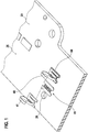
- Fig. 1 shows a perspective view of a printed circuit board 20 of an embodiment of the electronic control module 10 according to the invention.
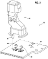
- Fig. 2 10 shows the printed circuit board 20 and the electronic component 30 before the electronic component 30 is arranged on the printed circuit board 20.
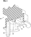
- Fig. 3 10 shows a cross-sectional view of the electronic component 30.
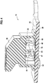
- Fig. 4 shows a cross-sectional view of an embodiment of the electronic control module 10 according to the invention before the application of potting material 80.
- the electronic control module 10 comprises a printed circuit board 20 and an electronic component 30, e.g. a sensor.
- the sensor can e.g. Record speeds and / or positions of tooth rims and / or switching elements, especially in gearboxes.
- the electronic control module 10 can in particular be a control module for a transmission, which is or will be arranged in the cavity of the transmission filled with a transmission oil.
- Two connecting elements 40, 41 are arranged on the printed circuit board 20.
- the connecting elements 40, 41 are electrically and mechanically connected to the printed circuit board 20 via reflow solder pads 60, 61 or reflow soldering.
- the left connecting element 40, 41 is not yet arranged on the solder pad 60, 61.
- the connecting elements 40, 41 are each designed to be resilient, so that they are in a direction perpendicular to the surface 25 of the printed circuit board 20 (in FIG Fig. 1 upwards or downwards) are designed to be resilient, ie reversibly yielding.
- the connecting elements 40, 41 are each designed as a so-called S-spring.
- the upper end region of the respective connecting element 40, 41 runs essentially parallel to the surface 25 of the printed circuit board 20.
- a recess 28 of the printed circuit board 20 is arranged, which through the printed circuit board 20 extends from the surface 25 of the printed circuit board 20 to Back 26 of the circuit board 20 runs.
- the recess 28 serves to receive a positioning pin 50 of the electronic component 30.
- the connecting elements 40, 41 are also designed to be movable or resilient in directions parallel to the surface 25 of the printed circuit board 20. In these directions, however, the respective connecting element 40, 41 is generally less resilient or can be deflected less far reversibly than in the direction perpendicular to the surface 25 of the printed circuit board 20.
- the electronic component 30 comprises a housing which houses the actual electronic component 30, e.g. partially or completely surrounds a sensor, an electronic circuit or the like.
- the electronic component 30 has two contact surfaces 35, 36 for electrically connecting the electronic component 30 to the connecting elements 40, 41 or the printed circuit board 20.
- the electronic component 30 is placed on the surface 25 of the printed circuit board 20 or arranged thereon in such a way that the two contact surfaces 35, 36 each contact or touch a connecting element 40, 41.
- the contact surface 35, 36 touches the respective upper end of the S-spring.
- the movement of the electronic component 30 when it is placed on the surface 25 of the printed circuit board 20 is shown in FIG Fig. 2 with a dashed line shown.
- the respective connecting element 40, 41 or the S-spring is compressed.
- the resilient design of the connecting element 40, 41 or the compression allows tolerances of the component 30 to be compensated for perpendicular to the surface 25 of the printed circuit board 20. Tolerances parallel to the surface 25 of the printed circuit board 20 can also be compensated for by the connecting elements 40, 41.
- the upper end piece of the respective connecting element 40, 41 contacts the contact surface 35, 36 of the electronic component 30, as shown in FIG Fig. 4 you can see.
- the connecting element 40, 41 and the contact surface 35, 36 are not mechanically connected to one another (for example soldered, welded, glued or the like), but the connecting element 40, 41 lies partly on the contact surface 35, 36 due to the spring force of the connecting element 40, 41 on or on the contact surface 35, 36.
- the electronic component 30 has a positioning pin 50 which projects vertically from a plane in which the contact surfaces 35, 36 are arranged.
- the positioning pin 50 serves to align the electronic component 30 in a first direction and a second direction perpendicular to the first direction, the first direction and the second direction being parallel to the surface 25 of the printed circuit board 20.
- the positioning pin 50 is at least partially in the recess 28 is arranged, the electronic component 30 can no longer be moved, but only rotated about the positioning pin 50 as an axis.
- a predetermined surface or edge of the electronic component 30 can also be aligned parallel to an edge of the printed circuit board 20.
- the electronic component 30 is also aligned in the direction around the positioning pin 50 as an axis.
- the electronic component 30 instead of aligning a surface or edge of the electronic component 30 with an edge of the printed circuit board 20, the electronic component 30 has a second positioning pin 50 and the printed circuit board 20 has a second recess 28, wherein when the electronic component 30 on the surface 25 of the circuit board 20, the second positioning pin 50 is inserted into the second recess 28.
- the electronic component 30 For alignment in a third direction, which is perpendicular to the first direction and perpendicular to the second direction, the electronic component 30 has a stop surface which contacts the surface 25 of the printed circuit board 20 when the electronic component 30 is in the correct position in FIG third direction is arranged.
- the positioning pin 50 is complementary to the recess 28 of the printed circuit board 20.
- the positioning pin 50 and the recess 28 can each have a circular cross section.
- An elliptical cross section is also possible, which enables even better alignment.
- the positioning pin 50 is inserted into the recess 28 in the printed circuit board 20 such that the positioning pin 50 projects beyond the rear side 26 of the printed circuit board 20.
- the part of the positioning pin 50 which protrudes beyond the rear side 26 of the printed circuit board 20 is heat-sealed, i.e. the part of the positioning pin 50 which protrudes beyond the rear side 26 of the printed circuit board 20 is pressed flat, so that the part of the positioning pin 50 which previously protrudes beyond the rear side 26 of the printed circuit board 20 then lies flat on the rear side 26 of the printed circuit board 20.
- This can e.g. by a warm stamp, a cold stamp and / or by hot air.
- the position of the electronic component 30 is now fixed in a direction perpendicular to the surface 25 of the printed circuit board 20, so that the positioning pin 50 can no longer be moved out of the recess 28.
- movement of the electronic component 30 parallel to the surface 25 of the printed circuit board 20 is no longer possible.
- turning around the positioning pin 50 is no longer possible.
- Fig. 4 shows the state after these steps.
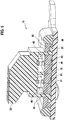
- Fig. 5 shows a cross-sectional view of an embodiment of the electronic control module 10 according to the invention after the application of potting material 80.
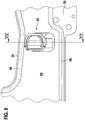
- Fig. 6 shows a top view of part of the electronic control module 10 Fig. 5 .
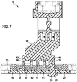
- Fig. 7 14 shows a cross-sectional view of the electronic control module 10 Fig. 6 along the line VII-VII.
- the cross-sectional view of the Fig. 7 is rotated 90 ° around a vertical axis in relation to the view that would result from a view of the plane VII-VII.
- a potting material 80 is applied in liquid or liquefied form to a part of the surface 25 of the printed circuit board 20 and then cured.
- An edge or wall 90 may previously have been applied to the surface 25 of the printed circuit board 20 in order to prevent the potting material 80 from flowing away or from flowing away before curing.
- the potting material 80 covers not only a part of the surface 25 of the printed circuit board 20, but also a part of the connecting elements 40, 41 and a protruding edge of the housing of the electronic component 30 (so-called hat brim), the protruding edge being part of the stop surface.
- hat brim a protruding edge of the housing of the electronic component 30
- the potting material 80 (e.g. a plastic) protects the respective connection between the connecting elements 40, 41 and the printed circuit board 20 against metal chips and aggressive liquids, e.g. Gear oil.
- An upper part protrudes from the potting material 80 from the connecting elements 40, 41, ie an upper part of the respective connecting element 40, 41 is not covered by the potting material 80.
- the upper end region of the respective connecting element 40, 41 which runs parallel to the surface 25 of the printed circuit board 20 and which is furthest away from the printed circuit board 20, is not covered or enclosed by the potting material 80 and is therefore still flexible or resilient.
- the different expansions or changes in size of the different elements (potting material 80, printed circuit board 20, reflow solder pad 60, 61, electronic component 30), which arise due to different thermal expansion coefficients of the different materials, can be compensated for even after casting with potting material 80 in the event of temperature changes .
- the electrical connection of the electronic component 30 to the printed circuit board 20 is therefore particularly (heat) stable.
- connection between connecting element 40, 41 and printed circuit board 20 soldering
- connection between connecting element 40, 41 and electronic component 30 pressing the resilient element against a contact surface 35, 36
- the electronic component 30 has a partition 70 on a side facing the printed circuit board 20 Fig. 5 perpendicular to the surface 25 of the circuit board 20.
- the partition 70 is arranged between the two contact surfaces 35, 36 of the electronic component 30.
- the potting material 80 is used on the surface 25 of the printed circuit board 20 at such a height that the area between the partition wall 70 and the surface 25 of the printed circuit board 20 is filled with potting material 80 (at the latest after the potting material 80 has hardened). This creates two chambers 45, 46, which are separated from one another by the partition wall 70.
- Each connecting element 40, 41 or each contact surface 35, 36 is thus arranged in its own chamber 45, 46.
- the chambers 45, 46 are partially open towards the surroundings, ie gear oil or the like can penetrate into the chambers 45, 46 from the outside.
- the contact surfaces 35, 36 of the electronic component 30 and at least the part of the connecting elements 40, 41 that are made of the potting material 80 protrude, have appropriate coatings (e.g. gold and / or tin) so that they do not corrode due to the gear oil.
- the circuit board 20 can e.g. be a printed circuit board (PCB).
- PCB printed circuit board
- the position of the connecting elements 40, 41 on the surface 25 of the printed circuit board 20 can already be determined when the layout of the printed circuit board 20 is determined by defining the reflow solder pads 60, 61.
- the connection elements 40, 41 are centered on the solder pads 60, 61 during reflow soldering.
- the connecting elements 40, 41 can thus be fixed on the printed circuit board 20 with a slight positional deviation and electrically contacted.
- the electronic components 30 can have very different overall heights.
- the arrangement of the electronic component 30 on the printed circuit board 20 can only take place shortly before the end of a process flow or shortly before the potting with potting material 80.
- standardized devices or devices and / or tools can be used before the electronic component 30 is arranged on the printed circuit board 20.
- the electronic control module 10 can in particular be or comprise a transmission control module.
Landscapes
- Engineering & Computer Science (AREA)
- Manufacturing & Machinery (AREA)
- Microelectronics & Electronic Packaging (AREA)
- Metallurgy (AREA)
- Structures For Mounting Electric Components On Printed Circuit Boards (AREA)
- Non-Metallic Protective Coatings For Printed Circuits (AREA)
Applications Claiming Priority (1)
| Application Number | Priority Date | Filing Date | Title |
|---|---|---|---|
| DE102018215149.0A DE102018215149A1 (de) | 2018-09-06 | 2018-09-06 | Elektronisches Steuermodul und Verfahren zum Herstellen eines elektronischen Steuermoduls |
Publications (2)
| Publication Number | Publication Date |
|---|---|
| EP3621160A1 true EP3621160A1 (fr) | 2020-03-11 |
| EP3621160B1 EP3621160B1 (fr) | 2024-04-10 |
Family
ID=67003216
Family Applications (1)
| Application Number | Title | Priority Date | Filing Date |
|---|---|---|---|
| EP19181756.8A Active EP3621160B1 (fr) | 2018-09-06 | 2019-06-21 | Module de commande électronique et procédé de fabrication d'un module de commande électronique |
Country Status (2)
| Country | Link |
|---|---|
| EP (1) | EP3621160B1 (fr) |
| DE (1) | DE102018215149A1 (fr) |
Cited By (2)
| Publication number | Priority date | Publication date | Assignee | Title |
|---|---|---|---|---|
| WO2022078556A1 (fr) * | 2020-10-13 | 2022-04-21 | Continental Automotive Gmbh | Procédé de fabrication d'un ensemble carte de circuit imprimé et connecteur |
| WO2023062009A1 (fr) * | 2021-10-11 | 2023-04-20 | Zf Friedrichshafen Ag | Module de détection |
Families Citing this family (2)
| Publication number | Priority date | Publication date | Assignee | Title |
|---|---|---|---|---|
| DE102021214109A1 (de) | 2021-12-10 | 2023-06-15 | Robert Bosch Gesellschaft mit beschränkter Haftung | Elektronische Baugruppe und Verfahren zur Herstellung einer elektronischen Baugruppe |
| DE102023102990A1 (de) * | 2023-02-08 | 2024-08-08 | Endress+Hauser Conducta Gmbh+Co. Kg | Elektronikmodul, Elektronikgerät und Elektroniksystem |
Citations (6)
| Publication number | Priority date | Publication date | Assignee | Title |
|---|---|---|---|---|
| DE102005036563A1 (de) * | 2005-08-03 | 2007-02-15 | Siemens Ag | Elektronisches Bauteil |
| US8203845B2 (en) * | 2008-01-10 | 2012-06-19 | Johnson Controls Technology Company | Electronics card comprising a printed circuit board and a piece of equipment carried by the board |
| EP3291654A1 (fr) * | 2016-08-29 | 2018-03-07 | Robert Bosch GmbH | Module de commande pour un véhicule automobile |
| DE102016224666A1 (de) * | 2016-12-12 | 2018-06-14 | Conti Temic Microelectronic Gmbh | Verfahren zur Herstellung einer Fügeverbindung sowie eine Fügeverbindung |
| CN108321572A (zh) * | 2017-12-19 | 2018-07-24 | 番禺得意精密电子工业有限公司 | 电连接器 |
| DE102017202962A1 (de) * | 2017-02-23 | 2018-08-23 | Robert Bosch Gmbh | Elektronikmodul sowie Verfahren zum Herstellen eines Elektronikmoduls |
-
2018
- 2018-09-06 DE DE102018215149.0A patent/DE102018215149A1/de not_active Withdrawn
-
2019
- 2019-06-21 EP EP19181756.8A patent/EP3621160B1/fr active Active
Patent Citations (7)
| Publication number | Priority date | Publication date | Assignee | Title |
|---|---|---|---|---|
| DE102005036563A1 (de) * | 2005-08-03 | 2007-02-15 | Siemens Ag | Elektronisches Bauteil |
| US8203845B2 (en) * | 2008-01-10 | 2012-06-19 | Johnson Controls Technology Company | Electronics card comprising a printed circuit board and a piece of equipment carried by the board |
| EP3291654A1 (fr) * | 2016-08-29 | 2018-03-07 | Robert Bosch GmbH | Module de commande pour un véhicule automobile |
| DE102016224666A1 (de) * | 2016-12-12 | 2018-06-14 | Conti Temic Microelectronic Gmbh | Verfahren zur Herstellung einer Fügeverbindung sowie eine Fügeverbindung |
| DE102017202962A1 (de) * | 2017-02-23 | 2018-08-23 | Robert Bosch Gmbh | Elektronikmodul sowie Verfahren zum Herstellen eines Elektronikmoduls |
| CN108321572A (zh) * | 2017-12-19 | 2018-07-24 | 番禺得意精密电子工业有限公司 | 电连接器 |
| US20190190207A1 (en) * | 2017-12-19 | 2019-06-20 | Lotes Co., Ltd | Electrical connector |
Cited By (3)
| Publication number | Priority date | Publication date | Assignee | Title |
|---|---|---|---|---|
| WO2022078556A1 (fr) * | 2020-10-13 | 2022-04-21 | Continental Automotive Gmbh | Procédé de fabrication d'un ensemble carte de circuit imprimé et connecteur |
| US12548928B2 (en) | 2020-10-13 | 2026-02-10 | Aumovio Germany Gmbh | Circuit-board-and-connector assembly and a method of producing thereof |
| WO2023062009A1 (fr) * | 2021-10-11 | 2023-04-20 | Zf Friedrichshafen Ag | Module de détection |
Also Published As
| Publication number | Publication date |
|---|---|
| EP3621160B1 (fr) | 2024-04-10 |
| DE102018215149A1 (de) | 2020-03-12 |
Similar Documents
| Publication | Publication Date | Title |
|---|---|---|
| EP3621160B1 (fr) | Module de commande électronique et procédé de fabrication d'un module de commande électronique | |
| DE102007026928B4 (de) | Harzgeformte Komponente, welche mit einer Metallplatte versehen ist und Form-bzw. Gießverfahren dafür | |
| DE102015219569B4 (de) | Elektronische Anordnung, Kombination und Verfahren zur Montage einer elektronischen Anordnung | |
| EP3479663B1 (fr) | Unité appareil de commande, en particulier pour un véhicule automobile | |
| EP3292593B1 (fr) | Dispositif de connexion électrique | |
| EP2772122A1 (fr) | Module de commande de transmission comprenant des ponts brasés ou des contacts froids entre le support de circuit inséré et le support de circuit environnant | |
| EP3574723B1 (fr) | Procédé de raccordement mécanique de composants électroniques et arrangement correspondant desdits composants électroniques | |
| DE102008014457A1 (de) | Schnittstelle | |
| EP3586577B1 (fr) | Module électronique et procédé de production d'un module électronique | |
| WO2015052117A1 (fr) | Commutation électronique | |
| WO2012130549A1 (fr) | Module électronique et procédé pour sa fabrication | |
| DE102019201404A1 (de) | Elektronikmodul | |
| EP2792222B1 (fr) | Appareil de commande d'un véhicule automobile | |
| WO2020043341A1 (fr) | Module électronique et son procédé de fabrication | |
| EP3643147B1 (fr) | Module électronique | |
| EP3610706B1 (fr) | Procédé de fabrication d'un module de capteur électronique | |
| EP3289840A1 (fr) | Module électronique pour appareil de commande de transmission | |
| WO2018059873A1 (fr) | Procédé de fabrication d'un composant électronique et composant électronique, en particulier pour un module de commande de boîte de vitesses | |
| EP3284327B1 (fr) | Module électronique pour dispositif de commande de transmission | |
| DE102016224799A1 (de) | Getriebesteuerungseinrichtung und Verfahren zum Befestigen eines Signaleingabeelements an einem Leiterplattenelement einer Getriebesteuerungseinrichtung | |
| DE102017204438A1 (de) | Verfahren zum Herstellen eines elektronischen Steuermoduls und elektronisches Steuermodul | |
| DE19623614C2 (de) | Intelligenter Schalter zum Einsatz in Bussystemen | |
| DE102016209488A1 (de) | Elektronikmodul mit Klemmverbindung für Getriebesteuergerät | |
| DE102023201588A1 (de) | Elektronikmodul | |
| EP2690413B2 (fr) | Capteur |
Legal Events
| Date | Code | Title | Description |
|---|---|---|---|
| PUAI | Public reference made under article 153(3) epc to a published international application that has entered the european phase |
Free format text: ORIGINAL CODE: 0009012 |
|
| STAA | Information on the status of an ep patent application or granted ep patent |
Free format text: STATUS: THE APPLICATION HAS BEEN PUBLISHED |
|
| AK | Designated contracting states |
Kind code of ref document: A1 Designated state(s): AL AT BE BG CH CY CZ DE DK EE ES FI FR GB GR HR HU IE IS IT LI LT LU LV MC MK MT NL NO PL PT RO RS SE SI SK SM TR |
|
| AX | Request for extension of the european patent |
Extension state: BA ME |
|
| RAP1 | Party data changed (applicant data changed or rights of an application transferred) |
Owner name: ROBERT BOSCH GMBH |
|
| STAA | Information on the status of an ep patent application or granted ep patent |
Free format text: STATUS: REQUEST FOR EXAMINATION WAS MADE |
|
| 17P | Request for examination filed |
Effective date: 20200911 |
|
| RBV | Designated contracting states (corrected) |
Designated state(s): AL AT BE BG CH CY CZ DE DK EE ES FI FR GB GR HR HU IE IS IT LI LT LU LV MC MK MT NL NO PL PT RO RS SE SI SK SM TR |
|
| GRAP | Despatch of communication of intention to grant a patent |
Free format text: ORIGINAL CODE: EPIDOSNIGR1 |
|
| STAA | Information on the status of an ep patent application or granted ep patent |
Free format text: STATUS: GRANT OF PATENT IS INTENDED |
|
| INTG | Intention to grant announced |
Effective date: 20240126 |
|
| GRAS | Grant fee paid |
Free format text: ORIGINAL CODE: EPIDOSNIGR3 |
|
| GRAA | (expected) grant |
Free format text: ORIGINAL CODE: 0009210 |
|
| STAA | Information on the status of an ep patent application or granted ep patent |
Free format text: STATUS: THE PATENT HAS BEEN GRANTED |
|
| AK | Designated contracting states |
Kind code of ref document: B1 Designated state(s): AL AT BE BG CH CY CZ DE DK EE ES FI FR GB GR HR HU IE IS IT LI LT LU LV MC MK MT NL NO PL PT RO RS SE SI SK SM TR |
|
| REG | Reference to a national code |
Ref country code: GB Ref legal event code: FG4D Free format text: NOT ENGLISH |
|
| REG | Reference to a national code |
Ref country code: CH Ref legal event code: EP |
|
| REG | Reference to a national code |
Ref country code: DE Ref legal event code: R096 Ref document number: 502019011004 Country of ref document: DE |
|
| REG | Reference to a national code |
Ref country code: IE Ref legal event code: FG4D Free format text: LANGUAGE OF EP DOCUMENT: GERMAN |
|
| REG | Reference to a national code |
Ref country code: LT Ref legal event code: MG9D |
|
| REG | Reference to a national code |
Ref country code: NL Ref legal event code: MP Effective date: 20240410 |
|
| PG25 | Lapsed in a contracting state [announced via postgrant information from national office to epo] |
Ref country code: NL Free format text: LAPSE BECAUSE OF FAILURE TO SUBMIT A TRANSLATION OF THE DESCRIPTION OR TO PAY THE FEE WITHIN THE PRESCRIBED TIME-LIMIT Effective date: 20240410 |
|
| PG25 | Lapsed in a contracting state [announced via postgrant information from national office to epo] |
Ref country code: NL Free format text: LAPSE BECAUSE OF FAILURE TO SUBMIT A TRANSLATION OF THE DESCRIPTION OR TO PAY THE FEE WITHIN THE PRESCRIBED TIME-LIMIT Effective date: 20240410 |
|
| PG25 | Lapsed in a contracting state [announced via postgrant information from national office to epo] |
Ref country code: IS Free format text: LAPSE BECAUSE OF FAILURE TO SUBMIT A TRANSLATION OF THE DESCRIPTION OR TO PAY THE FEE WITHIN THE PRESCRIBED TIME-LIMIT Effective date: 20240810 |
|
| PG25 | Lapsed in a contracting state [announced via postgrant information from national office to epo] |
Ref country code: BG Free format text: LAPSE BECAUSE OF FAILURE TO SUBMIT A TRANSLATION OF THE DESCRIPTION OR TO PAY THE FEE WITHIN THE PRESCRIBED TIME-LIMIT Effective date: 20240410 |
|
| PG25 | Lapsed in a contracting state [announced via postgrant information from national office to epo] |
Ref country code: FI Free format text: LAPSE BECAUSE OF FAILURE TO SUBMIT A TRANSLATION OF THE DESCRIPTION OR TO PAY THE FEE WITHIN THE PRESCRIBED TIME-LIMIT Effective date: 20240410 Ref country code: HR Free format text: LAPSE BECAUSE OF FAILURE TO SUBMIT A TRANSLATION OF THE DESCRIPTION OR TO PAY THE FEE WITHIN THE PRESCRIBED TIME-LIMIT Effective date: 20240410 |
|
| PG25 | Lapsed in a contracting state [announced via postgrant information from national office to epo] |
Ref country code: GR Free format text: LAPSE BECAUSE OF FAILURE TO SUBMIT A TRANSLATION OF THE DESCRIPTION OR TO PAY THE FEE WITHIN THE PRESCRIBED TIME-LIMIT Effective date: 20240711 |
|
| PG25 | Lapsed in a contracting state [announced via postgrant information from national office to epo] |
Ref country code: PT Free format text: LAPSE BECAUSE OF FAILURE TO SUBMIT A TRANSLATION OF THE DESCRIPTION OR TO PAY THE FEE WITHIN THE PRESCRIBED TIME-LIMIT Effective date: 20240812 |
|
| PG25 | Lapsed in a contracting state [announced via postgrant information from national office to epo] |
Ref country code: ES Free format text: LAPSE BECAUSE OF FAILURE TO SUBMIT A TRANSLATION OF THE DESCRIPTION OR TO PAY THE FEE WITHIN THE PRESCRIBED TIME-LIMIT Effective date: 20240410 |
|
| PG25 | Lapsed in a contracting state [announced via postgrant information from national office to epo] |
Ref country code: PL Free format text: LAPSE BECAUSE OF FAILURE TO SUBMIT A TRANSLATION OF THE DESCRIPTION OR TO PAY THE FEE WITHIN THE PRESCRIBED TIME-LIMIT Effective date: 20240410 |
|
| PG25 | Lapsed in a contracting state [announced via postgrant information from national office to epo] |
Ref country code: LV Free format text: LAPSE BECAUSE OF FAILURE TO SUBMIT A TRANSLATION OF THE DESCRIPTION OR TO PAY THE FEE WITHIN THE PRESCRIBED TIME-LIMIT Effective date: 20240410 |
|
| PG25 | Lapsed in a contracting state [announced via postgrant information from national office to epo] |
Ref country code: PT Free format text: LAPSE BECAUSE OF FAILURE TO SUBMIT A TRANSLATION OF THE DESCRIPTION OR TO PAY THE FEE WITHIN THE PRESCRIBED TIME-LIMIT Effective date: 20240812 Ref country code: PL Free format text: LAPSE BECAUSE OF FAILURE TO SUBMIT A TRANSLATION OF THE DESCRIPTION OR TO PAY THE FEE WITHIN THE PRESCRIBED TIME-LIMIT Effective date: 20240410 Ref country code: NO Free format text: LAPSE BECAUSE OF FAILURE TO SUBMIT A TRANSLATION OF THE DESCRIPTION OR TO PAY THE FEE WITHIN THE PRESCRIBED TIME-LIMIT Effective date: 20240710 Ref country code: LV Free format text: LAPSE BECAUSE OF FAILURE TO SUBMIT A TRANSLATION OF THE DESCRIPTION OR TO PAY THE FEE WITHIN THE PRESCRIBED TIME-LIMIT Effective date: 20240410 Ref country code: IS Free format text: LAPSE BECAUSE OF FAILURE TO SUBMIT A TRANSLATION OF THE DESCRIPTION OR TO PAY THE FEE WITHIN THE PRESCRIBED TIME-LIMIT Effective date: 20240810 Ref country code: HR Free format text: LAPSE BECAUSE OF FAILURE TO SUBMIT A TRANSLATION OF THE DESCRIPTION OR TO PAY THE FEE WITHIN THE PRESCRIBED TIME-LIMIT Effective date: 20240410 Ref country code: GR Free format text: LAPSE BECAUSE OF FAILURE TO SUBMIT A TRANSLATION OF THE DESCRIPTION OR TO PAY THE FEE WITHIN THE PRESCRIBED TIME-LIMIT Effective date: 20240711 Ref country code: FI Free format text: LAPSE BECAUSE OF FAILURE TO SUBMIT A TRANSLATION OF THE DESCRIPTION OR TO PAY THE FEE WITHIN THE PRESCRIBED TIME-LIMIT Effective date: 20240410 Ref country code: ES Free format text: LAPSE BECAUSE OF FAILURE TO SUBMIT A TRANSLATION OF THE DESCRIPTION OR TO PAY THE FEE WITHIN THE PRESCRIBED TIME-LIMIT Effective date: 20240410 Ref country code: BG Free format text: LAPSE BECAUSE OF FAILURE TO SUBMIT A TRANSLATION OF THE DESCRIPTION OR TO PAY THE FEE WITHIN THE PRESCRIBED TIME-LIMIT Effective date: 20240410 Ref country code: RS Free format text: LAPSE BECAUSE OF FAILURE TO SUBMIT A TRANSLATION OF THE DESCRIPTION OR TO PAY THE FEE WITHIN THE PRESCRIBED TIME-LIMIT Effective date: 20240710 |
|
| REG | Reference to a national code |
Ref country code: DE Ref legal event code: R097 Ref document number: 502019011004 Country of ref document: DE |
|
| PG25 | Lapsed in a contracting state [announced via postgrant information from national office to epo] |
Ref country code: DK Free format text: LAPSE BECAUSE OF FAILURE TO SUBMIT A TRANSLATION OF THE DESCRIPTION OR TO PAY THE FEE WITHIN THE PRESCRIBED TIME-LIMIT Effective date: 20240410 |
|
| PG25 | Lapsed in a contracting state [announced via postgrant information from national office to epo] |
Ref country code: EE Free format text: LAPSE BECAUSE OF FAILURE TO SUBMIT A TRANSLATION OF THE DESCRIPTION OR TO PAY THE FEE WITHIN THE PRESCRIBED TIME-LIMIT Effective date: 20240410 |
|
| PG25 | Lapsed in a contracting state [announced via postgrant information from national office to epo] |
Ref country code: CZ Free format text: LAPSE BECAUSE OF FAILURE TO SUBMIT A TRANSLATION OF THE DESCRIPTION OR TO PAY THE FEE WITHIN THE PRESCRIBED TIME-LIMIT Effective date: 20240410 |
|
| PG25 | Lapsed in a contracting state [announced via postgrant information from national office to epo] |
Ref country code: RO Free format text: LAPSE BECAUSE OF FAILURE TO SUBMIT A TRANSLATION OF THE DESCRIPTION OR TO PAY THE FEE WITHIN THE PRESCRIBED TIME-LIMIT Effective date: 20240410 Ref country code: SK Free format text: LAPSE BECAUSE OF FAILURE TO SUBMIT A TRANSLATION OF THE DESCRIPTION OR TO PAY THE FEE WITHIN THE PRESCRIBED TIME-LIMIT Effective date: 20240410 |
|
| PG25 | Lapsed in a contracting state [announced via postgrant information from national office to epo] |
Ref country code: SM Free format text: LAPSE BECAUSE OF FAILURE TO SUBMIT A TRANSLATION OF THE DESCRIPTION OR TO PAY THE FEE WITHIN THE PRESCRIBED TIME-LIMIT Effective date: 20240410 |
|
| PG25 | Lapsed in a contracting state [announced via postgrant information from national office to epo] |
Ref country code: SM Free format text: LAPSE BECAUSE OF FAILURE TO SUBMIT A TRANSLATION OF THE DESCRIPTION OR TO PAY THE FEE WITHIN THE PRESCRIBED TIME-LIMIT Effective date: 20240410 Ref country code: SK Free format text: LAPSE BECAUSE OF FAILURE TO SUBMIT A TRANSLATION OF THE DESCRIPTION OR TO PAY THE FEE WITHIN THE PRESCRIBED TIME-LIMIT Effective date: 20240410 Ref country code: RO Free format text: LAPSE BECAUSE OF FAILURE TO SUBMIT A TRANSLATION OF THE DESCRIPTION OR TO PAY THE FEE WITHIN THE PRESCRIBED TIME-LIMIT Effective date: 20240410 Ref country code: EE Free format text: LAPSE BECAUSE OF FAILURE TO SUBMIT A TRANSLATION OF THE DESCRIPTION OR TO PAY THE FEE WITHIN THE PRESCRIBED TIME-LIMIT Effective date: 20240410 Ref country code: DK Free format text: LAPSE BECAUSE OF FAILURE TO SUBMIT A TRANSLATION OF THE DESCRIPTION OR TO PAY THE FEE WITHIN THE PRESCRIBED TIME-LIMIT Effective date: 20240410 Ref country code: CZ Free format text: LAPSE BECAUSE OF FAILURE TO SUBMIT A TRANSLATION OF THE DESCRIPTION OR TO PAY THE FEE WITHIN THE PRESCRIBED TIME-LIMIT Effective date: 20240410 Ref country code: MC Free format text: LAPSE BECAUSE OF FAILURE TO SUBMIT A TRANSLATION OF THE DESCRIPTION OR TO PAY THE FEE WITHIN THE PRESCRIBED TIME-LIMIT Effective date: 20240410 |
|
| REG | Reference to a national code |
Ref country code: CH Ref legal event code: PL |
|
| PG25 | Lapsed in a contracting state [announced via postgrant information from national office to epo] |
Ref country code: IT Free format text: LAPSE BECAUSE OF FAILURE TO SUBMIT A TRANSLATION OF THE DESCRIPTION OR TO PAY THE FEE WITHIN THE PRESCRIBED TIME-LIMIT Effective date: 20240410 |
|
| PLBE | No opposition filed within time limit |
Free format text: ORIGINAL CODE: 0009261 |
|
| STAA | Information on the status of an ep patent application or granted ep patent |
Free format text: STATUS: NO OPPOSITION FILED WITHIN TIME LIMIT |
|
| PG25 | Lapsed in a contracting state [announced via postgrant information from national office to epo] |
Ref country code: LU Free format text: LAPSE BECAUSE OF NON-PAYMENT OF DUE FEES Effective date: 20240621 |
|
| 26N | No opposition filed |
Effective date: 20250113 |
|
| GBPC | Gb: european patent ceased through non-payment of renewal fee |
Effective date: 20240710 |
|
| PG25 | Lapsed in a contracting state [announced via postgrant information from national office to epo] |
Ref country code: IE Free format text: LAPSE BECAUSE OF NON-PAYMENT OF DUE FEES Effective date: 20240621 |
|
| PG25 | Lapsed in a contracting state [announced via postgrant information from national office to epo] |
Ref country code: SI Free format text: LAPSE BECAUSE OF FAILURE TO SUBMIT A TRANSLATION OF THE DESCRIPTION OR TO PAY THE FEE WITHIN THE PRESCRIBED TIME-LIMIT Effective date: 20240410 Ref country code: BE Free format text: LAPSE BECAUSE OF NON-PAYMENT OF DUE FEES Effective date: 20240630 Ref country code: CH Free format text: LAPSE BECAUSE OF NON-PAYMENT OF DUE FEES Effective date: 20240630 |
|
| PG25 | Lapsed in a contracting state [announced via postgrant information from national office to epo] |
Ref country code: GB Free format text: LAPSE BECAUSE OF NON-PAYMENT OF DUE FEES Effective date: 20240710 |
|
| REG | Reference to a national code |
Ref country code: BE Ref legal event code: MM Effective date: 20240630 |
|
| PGFP | Annual fee paid to national office [announced via postgrant information from national office to epo] |
Ref country code: FR Payment date: 20250618 Year of fee payment: 7 |
|
| REG | Reference to a national code |
Ref country code: AT Ref legal event code: MM01 Ref document number: 1675899 Country of ref document: AT Kind code of ref document: T Effective date: 20240621 |
|
| PG25 | Lapsed in a contracting state [announced via postgrant information from national office to epo] |
Ref country code: SE Free format text: LAPSE BECAUSE OF FAILURE TO SUBMIT A TRANSLATION OF THE DESCRIPTION OR TO PAY THE FEE WITHIN THE PRESCRIBED TIME-LIMIT Effective date: 20240410 |
|
| PGFP | Annual fee paid to national office [announced via postgrant information from national office to epo] |
Ref country code: DE Payment date: 20250814 Year of fee payment: 7 |
|
| PG25 | Lapsed in a contracting state [announced via postgrant information from national office to epo] |
Ref country code: AT Free format text: LAPSE BECAUSE OF NON-PAYMENT OF DUE FEES Effective date: 20240621 |
|
| PG25 | Lapsed in a contracting state [announced via postgrant information from national office to epo] |
Ref country code: CY Free format text: LAPSE BECAUSE OF FAILURE TO SUBMIT A TRANSLATION OF THE DESCRIPTION OR TO PAY THE FEE WITHIN THE PRESCRIBED TIME-LIMIT; INVALID AB INITIO Effective date: 20190621 |
|
| PG25 | Lapsed in a contracting state [announced via postgrant information from national office to epo] |
Ref country code: HU Free format text: LAPSE BECAUSE OF FAILURE TO SUBMIT A TRANSLATION OF THE DESCRIPTION OR TO PAY THE FEE WITHIN THE PRESCRIBED TIME-LIMIT; INVALID AB INITIO Effective date: 20190621 |