EP3622348B1 - Procédé et système de réduction de dépolarisation de fresnel pour améliorer le contraste d'image dans un système d'affichage comprenant de multiples affichages - Google Patents
Procédé et système de réduction de dépolarisation de fresnel pour améliorer le contraste d'image dans un système d'affichage comprenant de multiples affichages Download PDFInfo
- Publication number
- EP3622348B1 EP3622348B1 EP18802728.8A EP18802728A EP3622348B1 EP 3622348 B1 EP3622348 B1 EP 3622348B1 EP 18802728 A EP18802728 A EP 18802728A EP 3622348 B1 EP3622348 B1 EP 3622348B1
- Authority
- EP
- European Patent Office
- Prior art keywords
- display
- display device
- liquid crystal
- index
- matching material
- Prior art date
- Legal status (The legal status is an assumption and is not a legal conclusion. Google has not performed a legal analysis and makes no representation as to the accuracy of the status listed.)
- Active
Links
Images





Classifications
-
- G—PHYSICS
- G02—OPTICS
- G02B—OPTICAL ELEMENTS, SYSTEMS OR APPARATUS
- G02B5/00—Optical elements other than lenses
- G02B5/02—Diffusing elements; Afocal elements
- G02B5/0205—Diffusing elements; Afocal elements characterised by the diffusing properties
- G02B5/021—Diffusing elements; Afocal elements characterised by the diffusing properties the diffusion taking place at the element's surface, e.g. by means of surface roughening or microprismatic structures
- G02B5/0221—Diffusing elements; Afocal elements characterised by the diffusing properties the diffusion taking place at the element's surface, e.g. by means of surface roughening or microprismatic structures the surface having an irregular structure
-
- G—PHYSICS
- G02—OPTICS
- G02B—OPTICAL ELEMENTS, SYSTEMS OR APPARATUS
- G02B30/00—Optical systems or apparatus for producing three-dimensional [3D] effects, e.g. stereoscopic images
- G02B30/50—Optical systems or apparatus for producing three-dimensional [3D] effects, e.g. stereoscopic images the image being built up from image elements distributed over a three-dimensional [3D] volume, e.g. voxels
- G02B30/52—Optical systems or apparatus for producing three-dimensional [3D] effects, e.g. stereoscopic images the image being built up from image elements distributed over a three-dimensional [3D] volume, e.g. voxels the three-dimensional [3D] volume being constructed from a stack or sequence of two-dimensional [2D] planes, e.g. depth sampling systems
-
- G—PHYSICS
- G02—OPTICS
- G02B—OPTICAL ELEMENTS, SYSTEMS OR APPARATUS
- G02B5/00—Optical elements other than lenses
- G02B5/02—Diffusing elements; Afocal elements
- G02B5/0268—Diffusing elements; Afocal elements characterized by the fabrication or manufacturing method
-
- G—PHYSICS
- G02—OPTICS
- G02B—OPTICAL ELEMENTS, SYSTEMS OR APPARATUS
- G02B5/00—Optical elements other than lenses
- G02B5/02—Diffusing elements; Afocal elements
- G02B5/0273—Diffusing elements; Afocal elements characterized by the use
- G02B5/0278—Diffusing elements; Afocal elements characterized by the use used in transmission
-
- G—PHYSICS
- G02—OPTICS
- G02B—OPTICAL ELEMENTS, SYSTEMS OR APPARATUS
- G02B5/00—Optical elements other than lenses
- G02B5/02—Diffusing elements; Afocal elements
- G02B5/0273—Diffusing elements; Afocal elements characterized by the use
- G02B5/0294—Diffusing elements; Afocal elements characterized by the use adapted to provide an additional optical effect, e.g. anti-reflection or filter
-
- G—PHYSICS
- G02—OPTICS
- G02F—OPTICAL DEVICES OR ARRANGEMENTS FOR THE CONTROL OF LIGHT BY MODIFICATION OF THE OPTICAL PROPERTIES OF THE MEDIA OF THE ELEMENTS INVOLVED THEREIN; NON-LINEAR OPTICS; FREQUENCY-CHANGING OF LIGHT; OPTICAL LOGIC ELEMENTS; OPTICAL ANALOGUE/DIGITAL CONVERTERS
- G02F1/00—Devices or arrangements for the control of the intensity, colour, phase, polarisation or direction of light arriving from an independent light source, e.g. switching, gating or modulating; Non-linear optics
- G02F1/01—Devices or arrangements for the control of the intensity, colour, phase, polarisation or direction of light arriving from an independent light source, e.g. switching, gating or modulating; Non-linear optics for the control of the intensity, phase, polarisation or colour
- G02F1/13—Devices or arrangements for the control of the intensity, colour, phase, polarisation or direction of light arriving from an independent light source, e.g. switching, gating or modulating; Non-linear optics for the control of the intensity, phase, polarisation or colour based on liquid crystals, e.g. single liquid crystal display cells
- G02F1/133—Constructional arrangements; Operation of liquid crystal cells; Circuit arrangements
- G02F1/1333—Constructional arrangements; Manufacturing methods
- G02F1/1335—Structural association of cells with optical devices, e.g. polarisers or reflectors
-
- H—ELECTRICITY
- H04—ELECTRIC COMMUNICATION TECHNIQUE
- H04N—PICTORIAL COMMUNICATION, e.g. TELEVISION
- H04N13/00—Stereoscopic video systems; Multi-view video systems; Details thereof
- H04N13/30—Image reproducers
- H04N13/302—Image reproducers for viewing without the aid of special glasses, i.e. using autostereoscopic displays
- H04N13/307—Image reproducers for viewing without the aid of special glasses, i.e. using autostereoscopic displays using fly-eye lenses, e.g. arrangements of circular lenses
-
- G—PHYSICS
- G02—OPTICS
- G02B—OPTICAL ELEMENTS, SYSTEMS OR APPARATUS
- G02B27/00—Optical systems or apparatus not provided for by any of the groups G02B1/00 - G02B26/00, G02B30/00
- G02B27/09—Beam shaping, e.g. changing the cross-sectional area, not otherwise provided for
- G02B27/0927—Systems for changing the beam intensity distribution, e.g. Gaussian to top-hat
-
- G—PHYSICS
- G02—OPTICS
- G02B—OPTICAL ELEMENTS, SYSTEMS OR APPARATUS
- G02B27/00—Optical systems or apparatus not provided for by any of the groups G02B1/00 - G02B26/00, G02B30/00
- G02B27/60—Systems using moiré fringes
-
- G—PHYSICS
- G02—OPTICS
- G02B—OPTICAL ELEMENTS, SYSTEMS OR APPARATUS
- G02B5/00—Optical elements other than lenses
- G02B5/02—Diffusing elements; Afocal elements
- G02B5/0205—Diffusing elements; Afocal elements characterised by the diffusing properties
- G02B5/0257—Diffusing elements; Afocal elements characterised by the diffusing properties creating an anisotropic diffusion characteristic, i.e. distributing output differently in two perpendicular axes
-
- G—PHYSICS
- G02—OPTICS
- G02F—OPTICAL DEVICES OR ARRANGEMENTS FOR THE CONTROL OF LIGHT BY MODIFICATION OF THE OPTICAL PROPERTIES OF THE MEDIA OF THE ELEMENTS INVOLVED THEREIN; NON-LINEAR OPTICS; FREQUENCY-CHANGING OF LIGHT; OPTICAL LOGIC ELEMENTS; OPTICAL ANALOGUE/DIGITAL CONVERTERS
- G02F1/00—Devices or arrangements for the control of the intensity, colour, phase, polarisation or direction of light arriving from an independent light source, e.g. switching, gating or modulating; Non-linear optics
- G02F1/01—Devices or arrangements for the control of the intensity, colour, phase, polarisation or direction of light arriving from an independent light source, e.g. switching, gating or modulating; Non-linear optics for the control of the intensity, phase, polarisation or colour
- G02F1/13—Devices or arrangements for the control of the intensity, colour, phase, polarisation or direction of light arriving from an independent light source, e.g. switching, gating or modulating; Non-linear optics for the control of the intensity, phase, polarisation or colour based on liquid crystals, e.g. single liquid crystal display cells
- G02F1/133—Constructional arrangements; Operation of liquid crystal cells; Circuit arrangements
- G02F1/1333—Constructional arrangements; Manufacturing methods
- G02F1/1347—Arrangement of liquid crystal layers or cells in which the final condition of one light beam is achieved by the addition of the effects of two or more layers or cells
Definitions
- This invention relates to a multi-display system (e.g., a display including multiple display panels/display layers), where at least first and second displays (e.g., display panels or display layers) are arranged substantially parallel to each other in order to display three-dimensional (3D) features to a viewer(s).
- first and second displays e.g., display panels or display layers
- this invention relates generally to displays and, more particularly, to display systems and methods for displaying three-dimensional features.
- displays present information in two dimensions. Images displayed by such displays are planar images that lack depth information. Because people observe the world in three-dimensions, there have been efforts to provide displays that can display objects in three-dimensions. For example, stereo displays convey depth information by displaying offset images that are displayed separately to the left and right eye. When an observer views these planar images they are combined in the brain to give a perception of depth. However, such systems are complex and require increased resolution and processor computation power to provide a realistic perception of the displayed objects.
- Multi-component displays including multiple display screens in a stacked arrangement have been developed to display real depth.
- Each display screen may display its own image to provide visual depth due to the physical displacement of the display screens.
- multi-display systems are disclosed in prior art documents US 2015 / 0 323 805 A1 and US 2016 / 0 012 630 .
- US 2017 / 0 131 558 A1 discloses a method and a system using refractive beam mapper having square element profiles to reduce Moiré interference in a display system including multiple displays.
- US 2015 / 0 152 294 A1 describes heat-activatable siloxane-based adhesives.
- moire interference occurs.
- the moire interference is caused by interactions between the color filters within the layers when projected onto a viewer's retina. For example, when green color filters overlap, light is transmitted making for a comparative bright patch. When a green filter is over say a red filter, not as much light will be transmitted making for a dark region. Since the rear and front displays or display layers have slightly different sizes when projected onto the retina, the pixels will slowly change from being in phase to out of phase. This has the effect of producing dark and bright bands otherwise known as moire interference.
- the MLD system includes first and second displays.
- a refractive beam mapper may be utilized in order to reduce or eliminate moire interference.
- a display device comprising: a first display in a first plane for displaying a first image; a second display in a second plane for displaying a second image, wherein said first and second planes are approximately parallel to each other; and a beam mapping element (e.g., refractive beam mapper) located between the first and second displays and comprising a plurality of microlenses configured to direct incident rays from the second display in a pseudo random manner through sub-pixels of the first display and toward a viewer.
- a beam mapping element e.g., refractive beam mapper
- a refractive beam mapper may or may not be used in combination with other techniques for reducing moire interference (e.g., color filter offset or dissimilar color filter patterns on the respective displays, diffuser techniques, and/or subpixel compression) in various embodiments of this invention.
- moire interference e.g., color filter offset or dissimilar color filter patterns on the respective displays, diffuser techniques, and/or subpixel compression
- a multi-layered display device comprising: a first display layer in a first plane for displaying a first image; a second display layer in a second plane for displaying a second image, wherein said first and second planes are approximately parallel to each other; a refractive element located on a top surface of the first display layer or between the first and second display layers; and an index matching material between the first and second displays, the index matching material having a first refraction index that is higher than a refractive index of air and is from about 1.40 to 1.65.
- Each display layer is an LCD device.
- the index matching material may occupy the entire space, or substantially the entire space, between the first and second display layers.
- the first and/or display layer may be a liquid crystal display that includes a liquid crystal layer provided between at least first and second glass substrates, at least one of the glass substrates of the liquid crystal display having a second refractive index, and wherein the first refractive index of said index matching material does not differ from the second refractive index by more than 0.15, more preferably does not differ from the second refractive index by more than 0.10.
- the second refractive index may be from about 1.50 to 1.53, and the first refractive index may be at least 1.40 or at least 1.45.
- the index matching material may be free of, or substantially free of, birefringence.
- the index matching material may consists essentially of, or comprise, a silane or siloxane such as polydimethylsiloxane (PDMS).
- PDMS polydimethylsiloxane
- the refractive element e.g., microlens array
- This invention relates to a multi-display system (e.g., a display including multiple display panels), where at least first and second displays (e.g., display panels or display layers) are arranged substantially parallel to each other in order to display three-dimensional (3D) features to a viewer(s).
- the displays may be flat or curved in different embodiments.
- embodiments of this invention relate generally to displays and, more particularly, to display systems and methods for displaying three-dimensional features.
- MLDs according to example embodiments of this invention may be used, for example, as displays in vehicle dashes in order to provide 3D images (e.g., for speedometers, vehicle gauges, vehicle navigation displays, etc.).
- the color moiré interference problem is caused by the pattern regularity of both liquid crystal display (LCD) color filter arrays as, for example, RGB pixels are aligned into RGB columns in both displays of a MLD system. Color moiré interference may be largely prevalent in the horizontal direction.
- LCD liquid crystal display
- Figs. 1-3 illustrate an arrangement in a MLD system which experiences moire interference.
- Fig. 1 is a top plan view of color filters/pixels of a first liquid crystal display (LCD) where pixels or subpixels are the same color in each column.
- Fig. 1 shows a LCD having a conventional red-green-blue (R-G-B) repeating pattern or arrangement, wherein the pixels or subpixels are the same color in each column.
- R-G-B red-green-blue
- the color filter stripes are arranged in vertical lines in a BGR order, and this BGR order repeats itself over and over moving from left to right across the display of Fig. 1 .
- a subpixel may be considered the area of a given pixel electrode in an area of a particular color filter. For instance, R, G and B subpixels may make up a pixel. Alternatively, a subpixel may be considered to be a pixel.
- FIG. 1 is shown without color mask rotation. Conventionally, both panels of a multiple layered display (MLD) may be configured similarly with such a R-G-B arrangement.
- the repeatable pattern may be R-G-B, or R-B-G, or any other combination.
- Fig. 2 is a top plan view of color filters/pixels/subpixels of a second LCD where pixels or subpixels are also the same color in each column.
- the color filter stripes are arranged in vertical lines in a RGB order, and this order repeats itself over and over moving from left to right across Fig. 2 .
- the repeatable pattern may be R-G-B, or R-B-G, or any other combination involving these colors.
- green (G) columns are located between blue (B) and red (R) colored columns.
- Fig. 3 is a top plan view of a MLD system resulting from the combination of the LCDs of Figs. 1 and 2 , one on top of the other in a stacked overlapping relationship in a MLD system.
- Fig. 3 shows the mixing of the color filter and pixel/subpixel patterns shown in Figs. 1 and 2 .
- Fig. 3 illustrates the emergence of moiré interference given an instance where both LCDs have a similar R-G-B column arrangement, where the pixels are the same color in each column.
- green color filter lines overlap (e.g., see the left portion of Fig.
- Example embodiments of this invention address, and reduce or solve, this moire interference problem.
- Certain example embodiments of the instant invention provide solution(s) that make moiré interference in MLD systems vanish or substantially vanish, but without significantly sacrificing the rear display resolution and contrast.
- a beam mapping element such as diffractive optical element (DOE) or a refractive beam mapper (RBM) composed of many micro-lenses may be used to reduce moire interference.
- DOE diffractive optical element
- RBM refractive beam mapper
- pseudo random mapping may be provided in order to not introduce extra moiré effects.
- the divergence of individual beams may be limited so that any point on the rear LCD is not diverted more than one pixel distance from a straight line by the time it reaches the front LCD in certain example embodiments.
- One may also laminate such a beam mapping element to the front display and optically match the media between the two LCDs with a non-birefringent material in certain example embodiments, and such embodiments may or may not be used in combination with subpixel compression techniques discussed herein.
- Twisted nematic (TN) LCDs may follow a fairly generic pixel layout, such as a square divided into three portions running horizontally (or vertically) with red green and blue sub-pixels. The sub-pixels may be separated by a black mask in the horizontal and vertical directions. There is often a square protrusion in the corner of the sub-pixel to cover the drive transistor.
- pixel technology that enable wide screen viewing and temporal performance required for modern desktop monitors and televisions.
- Embodiments of the present invention are compatible with all of these LCDs, since the backplanes are designed to follow the basic RGB stripe pixel layout. As such, the backplane layout required for each pixel does not need to change.
- pixel type displays by manufacturer include: Panasonic (IPS Pro), LG Display (H-IPS & P-IPS), Hannstar (S-IPS), AU Optronics (A-MVA), Samsung (AFFS), S-LCD (S-PVA), and Sharp Corporation (ASV and MVA).
- both displays or display layers may be OLEDs, or one display may be an OLED and the other an LCD. Note that in OLEDs, respective sub-pixels or pixels would be filled with red, green, and blue material as the color filter material (as opposed to having LCD type color filters).
- Fig. 6 illustrates a MLD according to an example embodiment of this invention, in which the stacked overlapping layers/displays of any of the figures herein may be provided and utilized.
- the displays shown in any of Figs. 4-5 and 14-16 may be the front 1 and rear 2 displays in Fig. 6 , respectively.
- the first display or display layer of the MLD may be element 1 (or 2), and the second display or display layer of the MLD may be element 2 (or 1).
- Display or display layer 2 is closest to the backlight of the MLD, and it may be desirable to have its backplane facing the backlight system to recycle light that may pass through row drivers, column drivers, transistors, and storage capacitance lines into the backlight.
- a two polarizer configuration may be used, as shown in the figure, and gaps may be designed to include air or material having birefringence designed to maintain black state of the display when desired.
- the gap may include material having a refractive index matched closely to glass or the layers on either side to reduce internal reflection and/or depolarization effects.
- its backplane may be oriented opposite to that of display or display layer 2.
- its backplane may be oriented to face the viewer to reduce internal reflections.
- the color filter layers (each of which may be made up of one or more layers) of the respective displays 1 and 2 may be designed to face each other, with no liquid crystal layer from either display being located between the color filter layers of the first and second displays in certain example embodiments.
- an antireflective system at the front such as that shown in Fig. 6 made up of quarter wave retarder and an antireflective (AR) polarizer, so that ambient light that would normally be reflected would undergo a quarter wave rotation on the first pass through the AR polarizer, is reflected by the backplane elements, undergoes a second rotation through the quarter wavelength retarder.
- AR antireflective
- AR antireflective coating(s) may be applied to the interior surfaces in certain example embodiments of this invention.
- the AR coating may, for example, operate in the visible range, e.g., moth eye, single layer interference, multi-layer interference, etc.
- a beam mapping element is made up of, or includes, a plurality of micro ⁇ lenses and may be used as a stand-alone element for reducing moire interference via pseudo random mapping (e.g., see Figs. 4-6 and 14-16 ).
- pseudo random mapping embodiments e.g., Figs. 4-5
- each of the refractive micro ⁇ lenses of an RBM may be designed to direct incident rays from the back LCD 2 to an observer in a defined path, each ray passing through a different sub ⁇ pixel in the front LCD 1 according to a pseudo random mapping.
- the RBM may be laminated to the top LCD 1 (see Figs. 5 , 14 and 16 ), and optionally matched or substantially matched optically to media between the two LCDs with a nonDbirefringent material.
- the refractive beam mapper can be placed anywhere within the LCD stack.
- Fig. 5 shows the beam mapping element (e.g., RBM including a micro-lens array) located between the front and rear LCDs and laminated to an interior side of the front display.
- RBM including a micro-lens array
- the micro-lenses of an RBM may be fabricated using gray-scale lithography, to produce arbitrary surface structures in a micro-lens format.
- Each lens element may configured for directing light in a controlled direction enabling arbitrary and asymmetric scattering angles as shown in Figs. 4-5 .
- profile slope angle is more important than profile height.
- Figs. 4-5 show how the refractive beam mapper superimposes rays from the back LCD 2 onto the front LCD 1 from an observer's point of view. The beam paths are mapped in a pseudo random fashion so not to introduce other artifacts such as extra moiré.
- the underlying LCD structure 2 is randomized and thus incapable of generating significant moiré interference with the top LCD 1.
- a diffuser may instead be used for the construction of a moiré suppression element. While the process can be adapted to make a refractive beam mapper, engineered diffusers can also be used as optimal diffuser elements for more reduction. Diffusers are not as desirable as a refractive beam element.
- the refractive beam mapper may exhibit various features.
- an RBM may exhibit achromatic performance.
- an RBM may exhibit arbitrary/asymmetric scattering angles.
- an RBM may exhibit controlled intensity distribution patterns (e.g., circular, square, rectangular, elliptical, line, ring, etc.).
- an RBM may exhibit controlled intensity profiles (e.g., flat top, Gaussian, batwing, custom, etc.).
- An RBM may also exhibit high optical transmission efficiency (e.g., 90 percent).
- an RBM may exhibit the preservation of polarization.
- An RBM may be of or include various materials, such as polymer injection molding, hot embossed polymers, polymer-on-glass components, etc.
- Moiré interference in MLD is commonly suppressed by adding a diffuser element (as opposed to a beam mapping element) between the back LCD and the observer so that the pixel structure in the back LCD is blurred.
- Fig. 7 illustrates a bandwidth limited implementation of an RBM having custom refractive optics which are close to a flat top profile, such that the far field pattern is as close as possible to a flat top profile.
- the prescription for the set of lenses that comprise the distribution is defined, including feature sizes and slope angles based on the scatter requirements. These parameters may be defined in terms of probability distribution functions that specify the likelihood that a certain lens will assume a specific prescription.
- a spatial distribution of the microlenses to create the surface structure is designed to create the surface structure according to a desired distribution function. It is appreciated that any underlying periodicity in the spatial distribution of the microlenses may be eliminated in certain example embodiments. Also, lens mismatches may be eliminated, wherein lens mismatches can lead to wide-angle scatter, are eliminated.
- the careful pseudo randomization of the surface structure also creates a scatter distribution that is devoid of artifacts and induced moiré. This may be significant as regular patterns can introduce additional moiré interference.
- Fig. 9 shows that there is a tradeoff between microlens size and introduced image artifacts. Bigger microlenses will typically have better anti-moiré diffuser profiles. If the microlenses become of a size that are visible to the naked eye, then extra image artifacts will become apparent. These include sparkle, pixel walking and moiré interference between the pattern and either or both LCDs.
- Fig. 9 illustrates PSF for a single microlens for various values of diameters (um). Curves 901, 902 and 903 represent diameters 500, 50 and 5, respectively. Minimizing feature size may also be utilized in the design of an LCD moiré reduction element. The feature size should ideally be smaller than a sub pixel in order to remain substantially invisible to the naked eye as shown in Fig.
- the feature size is given by the microlens diameter.
- miniature refractive elements are desired. If the microlenses become of a size that are visible to the naked eye then extra image artifacts will become apparent. These include sparkle, pixel walking, and moiré interference between the pattern and either or both LCDs. Sparkle is most often seen in anti-glare displays where the display surface has been treated to produce a matte textured surface. These surface features act as refractive or diffractive elements and can either focus or defocus individual pixel elements depending on the viewer position leading to intensity variations or sparkle. Pixel walking is the result of the refractive distortion appearing to move and distort the individual pixels and the viewer moves position.
- Extra moiré interference is introduced when regular features in the array of microlens "beat" with one or both of the LCDs. Randomization and reduction of lens size in an RBM or diffuser and placement reduce these extra moiré artifacts. There are two factors to consider in this regard, sag and averaging. To ensure the best uniformity and reduction in moiré, a large number of scatter centers should be illuminated within each pixel area as shown in Fig. 4 . At the same time, for a certain set of parameters (e.g., spread angle, index of refraction, and conic constant), the lens depth decreases as the microlens diameter decreases. If the process continues, a diffractive regime is eventually reached where the lens depth only imparts a phase delay that is a small fraction of 2 ⁇ . In this respect, it is useful to define the phase number in the following equation:
- y max represents the total lens sag
- ⁇ is the wavelength under consideration
- ⁇ n equals n( ⁇ )1, with n the index of refraction at wavelength ⁇ , for an element in air.
- the phase number M should be as large as possible.
- ⁇ 0 is the half width beam spread angle in degrees (in air).
- Embedding the refractor in a medium of higher refractive index (PI) such as silicon OCA, rather than air, allows for the effective use of a wider angle refractor, as the higher RI will reduce the refractive power of each microlens.
- PI refractive index
- embedding in high RI material effectively reduces the microlens diameter, which results in less image artifacts.
- replacing the air between the two panels with an indexed matched medium will also allow smaller divergence angles as measured in air and thus smaller microlens diameters.
- Fig. 10 shows the fabrication process of an RBM, in accordance with one embodiment of the present disclosure in the above respects, including the formation of microlenses on a wafer support.
- the RBM may be embedded in high RI material to reduce Fresnel depolarization, in order to improve image contrast of the MLD.
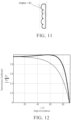
- Fig. 11 shows a microlens surface, which typically has a distribution of surface normals between 0 and approximately 20 degrees. The distribution of surface normals leads to contrast reduction because S and P polarizations are transmitted with different attenuations.
- Fig. 12 shows curves illustrating the transmission coefficient for S and P waves vs. angle of incidence
- Fig. 13 shows system contrast (contrast( ⁇ i, n1, n2, N)), wherein ⁇ i is the angle of incidence, n1 is the refractive index of the material between LCDs, n2 is the refractive index of glass, and N is the number of interfaces.
- the line to the far right with the RI at 1.4 and 1.5 shows the best contrast as the Fresnel depolarization is the least.
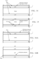
- Figs. 14-16 show various placements of the moiré reduction element (e.g., refractive element such as RBM).
- the moiré reduction element could be positioned on the top surface of the front display 1 as a laminatable film with the patterned surface facing downwards to get the feature size small, as previously described.
- FIG. 16A shows, for example, the moiré reduction element positioned facing up in optical coupling adhesive (OCA).
- OCA optical coupling adhesive
- the cover glass may be bonded to OCA.
- FIG. 16B shows another example of the placement of the refractive element. Light is absorbed by the polarizer if internally reflected by the reflective element.
- ⁇ may or may not be used in combination with subpixel compression techniques.
- having the patterned surface facing upwards would also act as an anti-glaring mechanism, but it will be necessary to embed in OCA with a refractive index of approximately 1.5 to achieve a feature size smaller than 70 ⁇ m.
- Index matching the internal voids with a material of R.I. greater than 1.4 will greatly reduce Fresnel depolarization, thereby improving contrast and reducing reflections.
- the internal voids index matched with glass and OCA to reduce Fresnel polarization also improve contrast and reduce reflections.
- the FWHM width for this implementation may be about 1.8 degrees, with a square profile.
- IPS In Plane Switching
- both reflection and refraction of the light may occur, as shown in FIG. 17 .
- the figure shows the case when n2 > n1 and where external reflection occurs of the incident ray.
- the incident ray has a ⁇ i angle of incidence at the interface between the medium of n1 refractive index and the medium of n2 refractive index.
- the corresponding reflected ray has a ⁇ r angle of reflection, and the corresponding transmitted ray has a ⁇ t angle of transmission.
- the figure also shows the plane of incidence.
- Fresnel equations describe what fraction of the light is reflected and what fraction is refracted (i.e., transmitted). They also describe the phase shift of the reflected light.
- the incident light is polarized with its electric field perpendicular to the plane containing the incident ray, reflected ray, and refracted rays. This plane is referred to as the plane of incidence.
- FIG. 18 provides another illustration of the relationship between the incident ray 1801, reflected ray 1802 and the transmitted ray 1803 in the plane of incidence 1806.
- the light is said to be s-polarized, from the German senkrecht ("perpendicular").
- the incident light is polarized with its electric field parallel to the plane of incidence. Such light is described as p-polarized, from parallel.
- an incident light ray IO strikes the interface between two media of refractive indices n 1 and n 2 at point O. Part of the incident ray is reflected as ray OR and part refracted as ray OT.
- the angles that the incident, reflected and refracted rays make to the normal 1805 of the interface 1804 are given as ⁇ i , ⁇ r and ⁇ t , respectively. The relationship between these angles is given by the law of reflection. and Snell's Law:
- the reflectance or reflectivity R The fraction of the incident power that is reflected from the interface is given by the reflectance or reflectivity R and the fraction that is refracted is given by the transmittance or transmissivity T (note that T is unrelated to the transmission through a medium).
- the reflectance for s-polarized light becomes:
- the reflectance for s-polarized light becomes:
- the reflectance for s-polarized light becomes:
- FIG. 19 shows diagrams for transmitted light T s and T p .
- FIG. 19B shows light going from a less dense to a more dense medium e.g. from air into glass. It can be seen that light is transmitted for both the S and P waves up to about an angle of incidence of 60 degrees. However note that the transmission of the S and P waves is different, which results in the rotation as talked about below (since the final rotation is the vector sum of the s and p states). Ditto with the second example however this is going from a dense to a less dense medium e.g. glass to air and as such the transmission cuts of completely at ⁇ 42 degrees, which is when the material starts totally internally reflecting.
- the plane of incidence for any ray entering the observer's eye will be a plane formed by the three points A, B and C where A is the closest point from the eye on the LCD surface, B the ray exit point on the LCD and C the eye.
- Line AC is normal to the LCD surface, as shown in FIG. 21 .
- This plane is perpendicular to the LCD surface but can be at any angle perpendicular to the LCD surface.
- the amount of attenuation is dependent on incident angle ACB and also the orientation of line AB to the ray polarization.
- s-polarization and p-polarization directions are either aligned or not aligned.
- TD polarization transmission direction
- p-polarization is aligned and therefore transmitted
- s-polarization is aligned and therefore transmitted.
- the backplane layer of the LCD is more reflective than the top color plane as the backplane apertures are framed with reflective metallization and the color plane aperture is framed with matt black material.
- the top layer is flipped so the reflective metallization is facing upwards.
- the top layer is customized so the aperture is framed with matt black material.
- FIG. 23 shows the effective contrast ratio due the Fresnel effects alone with different amount of layers and refractive index materials of 1.0 (air) up to 1.4 (PDMSPolydimethylsiloxane).
- air glass interface is a problem causing issues with the contrast and removing the air and replacing with birefringent free index matching material of R.I. greater than or equal to 1.4 greatly improves contrast.
- the air may be replaced with a material that has a RI within a certain threshold margin of the RI of the LCD glass. In this example, with glass RI at 1.5, the threshold RI for index matching may be 1.4.
Landscapes
- Physics & Mathematics (AREA)
- General Physics & Mathematics (AREA)
- Optics & Photonics (AREA)
- Engineering & Computer Science (AREA)
- Nonlinear Science (AREA)
- Multimedia (AREA)
- Signal Processing (AREA)
- Mathematical Physics (AREA)
- Chemical & Material Sciences (AREA)
- Crystallography & Structural Chemistry (AREA)
- Manufacturing & Machinery (AREA)
- Liquid Crystal (AREA)
Claims (20)
- Dispositif d'affichage multicouche, comprenant :une première couche d'affichage (1) dans un premier plan pour afficher une première image, dans lequel la première couche d'affichage est un premier affichage à cristaux liquides ;une deuxième couche d'affichage (2) dans un deuxième plan pour afficher une deuxième image, dans lequel la deuxième couche d'affichage est un deuxième affichage à cristaux liquides, dans lequel lesdits premier et deuxième plans sont approximativement parallèles l'un à l'autre ;un élément réfringent situé sur une surface supérieure de la première couche d'affichage ou entre les première et deuxième couches d'affichage ; etun matériau d'adaptation d'indice entre les premier et deuxième affichages, le matériau d'adaptation d'indice ayant un premier indice de réfraction qui est supérieur à un indice de réfraction de l'air et est compris entre environ 1,40 et 1,65,caractérisé en ce que le matériau d'adaptation d'indice est plus large et plus haut que le premier affichage à cristaux liquides et le deuxième affichage à cristaux liquides.
- Dispositif d'affichage multicouche selon la revendication 1, dans lequel le matériau d'adaptation d'indice occupe la totalité de l'espace entre les première et deuxième couches d'affichage.
- Dispositif d'affichage multicouche selon l'une quelconque des revendications précédentes, dans lequel le premier affichage à cristaux liquides inclut une couche de cristaux liquides prévue entre au moins un premier et un deuxième substrat de verre, au moins l'un des substrats de verre du premier affichage à cristaux liquides ayant un deuxième indice de réfraction, et dans lequel le premier indice de réfraction dudit matériau d'adaptation d'indice ne diffère pas du deuxième indice de réfraction de plus de 0,15.
- Dispositif d'affichage multicouche selon la revendication 3, dans lequel le premier indice de réfraction dudit matériau d'adaptation d'indice ne diffère pas du deuxième indice de réfraction de plus de 0,10.
- Dispositif d'affichage multicouche selon l'une quelconque des revendications 3 à 4, dans lequel le deuxième indice de réfraction est compris entre environ 1,50 et 1,53, et dans lequel le deuxième indice de réfraction est d'au moins 1,45.
- Dispositif d'affichage multicouche selon l'une quelconque des revendications précédentes, dans lequel le matériau d'adaptation d'indice est exempt, ou sensiblement exempt, de biréfringence.
- Dispositif d'affichage multicouche selon l'une quelconque des revendications précédentes, dans lequel le matériau d'adaptation d'indice consiste essentiellement en, ou comprend, du polydiméthylsiloxane (PDMS).
- Dispositif d'affichage multicouche selon l'une quelconque des revendications précédentes, dans lequel le matériau d'adaptation d'indice consiste essentiellement en, ou comprend, un silane et/ou un siloxane.
- Dispositif d'affichage multicouche selon l'une quelconque des revendications précédentes, dans lequel l'élément réfringent est directement en contact avec le matériau d'adaptation d'indice pour réduire la dépolarisation de Fresnel.
- Dispositif d'affichage multicouche selon l'une quelconque des revendications précédentes, dans lequel l'élément réfringent est incorporé dans le matériau d'adaptation d'indice.
- Dispositif d'affichage multicouche selon l'une quelconque des revendications précédentes, dans lequel l'élément réfringent comprend une pluralité de microlentilles configurées pour diriger les rayons émis par le deuxième affichage d'une manière pseudo-aléatoire à travers des sous-pixels du premier affichage et vers un observateur.
- Dispositif d'affichage multicouche selon la revendication 11, dans lequel les microlentilles ont une distribution de normales à la surface comprise entre 0 et environ 20 degrés.
- Dispositif d'affichage multicouche selon l'une quelconque des revendications 11 à 12, dans lequel des surfaces incurvées des microlentilles sont en contact avec le matériau d'adaptation d'indice.
- Dispositif d'affichage multicouche selon l'une quelconque des revendications précédentes, dans lequel l'élément réfringent est configuré pour préserver sensiblement la polarisation.
- Dispositif d'affichage multicouche selon l'une quelconque des revendications précédentes, dans lequel l'élément réfringent est laminé sur la première ou la deuxième couche d'affichage.
- Dispositif d'affichage multicouche selon l'une quelconque des revendications précédentes, dans lequel la deuxième couche d'affichage est un affichage arrière, et la première couche d'affichage est un affichage avant, du dispositif d'affichage.
- Dispositif d'affichage multicouche selon l'une quelconque des revendications précédentes, dans lequel le deuxième affichage à cristaux liquides inclut une couche de cristaux liquides prévue entre au moins un premier et un deuxième substrat de verre, au moins l'un des substrats de verre du deuxième affichage à cristaux liquides ayant un deuxième indice de réfraction, et dans lequel le premier indice de réfraction dudit matériau d'adaptation d'indice ne diffère pas du deuxième indice de réfraction de plus de 0,15.
- Procédé de formation d'un dispositif d'affichage multicouche, le procédé comprenant les étapes consistant à :fournir une première couche d'affichage dans un premier plan pour afficher une première image, dans lequel la première couche d'affichage est un premier affichage à cristaux liquides, et une deuxième couche d'affichage dans un deuxième plan pour afficher une deuxième image, dans lequel la deuxième couche d'affichage est un deuxième affichage à cristaux liquides, dans lequel lesdits premier et deuxième plans sont approximativement parallèles l'un à l'autre ;fournir un élément réfringent disposé sur une surface supérieure de la première couche d'affichage ou entre les première et deuxième couches d'affichage ; etfournir un matériau d'adaptation d'indice entre les premier et deuxième affichages, le matériau d'adaptation d'indice ayant un premier indice de réfraction qui est différent d'un indice de réfraction de l'air ;caractérisé en ce que le matériau d'adaptation d'indice est plus large et plus haut que le premier affichage à cristaux liquides et le deuxième affichage à cristaux liquides.
- Procédé selon la revendication 18, dans lequel le matériau occupe la totalité de l'espace entre les première et deuxième couches d'affichage.
- Procédé selon la revendication 18, dans lequel le premier et/ou le deuxième affichage à cristaux liquides ont un deuxième indice de réfraction, et dans lequel le premier indice de réfraction se situe dans une marge de seuil prédéterminée par rapport au deuxième indice de réfraction.
Applications Claiming Priority (2)
| Application Number | Priority Date | Filing Date | Title |
|---|---|---|---|
| US15/597,587 US20170351106A1 (en) | 2015-10-02 | 2017-05-17 | Method and system for reducing fresnel depolarization to improve image contrast in a display system including multiple displays |
| PCT/US2018/032910 WO2018213407A1 (fr) | 2017-05-17 | 2018-05-16 | Procédé et système de réduction de dépolarisation de fresnel pour améliorer le contraste d'image dans un système d'affichage comprenant de multiples affichages |
Publications (3)
| Publication Number | Publication Date |
|---|---|
| EP3622348A1 EP3622348A1 (fr) | 2020-03-18 |
| EP3622348A4 EP3622348A4 (fr) | 2021-04-21 |
| EP3622348B1 true EP3622348B1 (fr) | 2023-05-10 |
Family
ID=64274813
Family Applications (1)
| Application Number | Title | Priority Date | Filing Date |
|---|---|---|---|
| EP18802728.8A Active EP3622348B1 (fr) | 2017-05-17 | 2018-05-16 | Procédé et système de réduction de dépolarisation de fresnel pour améliorer le contraste d'image dans un système d'affichage comprenant de multiples affichages |
Country Status (3)
| Country | Link |
|---|---|
| EP (1) | EP3622348B1 (fr) |
| CN (1) | CN111183391A (fr) |
| WO (1) | WO2018213407A1 (fr) |
Families Citing this family (2)
| Publication number | Priority date | Publication date | Assignee | Title |
|---|---|---|---|---|
| CN113866997B (zh) * | 2021-09-17 | 2023-10-24 | 深圳技术大学 | 显示系统 |
| CN121050083B (zh) * | 2025-11-04 | 2026-02-13 | 中国科学院长春光学精密机械与物理研究所 | 水下透射光学成像系统 |
Family Cites Families (16)
| Publication number | Priority date | Publication date | Assignee | Title |
|---|---|---|---|---|
| KR100234896B1 (ko) * | 1997-07-29 | 1999-12-15 | 구본준 | 액정표시장치의 기판 평탄화 방법 |
| NZ514500A (en) * | 2001-10-11 | 2004-06-25 | Deep Video Imaging Ltd | A multiplane visual display unit with a transparent emissive layer disposed between two display planes |
| WO2003079094A2 (fr) * | 2002-03-17 | 2003-09-25 | Deep Video Imaging Limited | Procede de commande de la fonction d'etalement de point d'une image |
| EP1540407A4 (fr) * | 2002-07-15 | 2009-01-07 | Puredepth Ltd | Ecran video multicouche ameliore |
| US20060203338A1 (en) * | 2005-03-12 | 2006-09-14 | Polaris Sensor Technologies, Inc. | System and method for dual stacked panel display |
| WO2007108162A1 (fr) * | 2006-03-22 | 2007-09-27 | Sharp Kabushiki Kaisha | Dispositif d'affichage de type composite et récepteur de télévision |
| JP5176194B2 (ja) * | 2006-04-18 | 2013-04-03 | Nltテクノロジー株式会社 | 液晶表示装置及び画像表示システム |
| US7916223B2 (en) * | 2006-04-18 | 2011-03-29 | Nec Lcd Technologies, Ltd. | Dual panel liquid crystal display device |
| JP4981394B2 (ja) * | 2006-09-28 | 2012-07-18 | 株式会社ジャパンディスプレイイースト | 表示装置 |
| CN104411791B (zh) * | 2012-07-03 | 2017-06-09 | 3M创新有限公司 | 可热活化的硅氧烷基粘合剂 |
| US9519154B2 (en) | 2014-05-09 | 2016-12-13 | Pure Depth Limited | Diffraction grating for use with a multi-layered display system |
| CN108474943B (zh) * | 2015-10-02 | 2021-04-27 | 安波福技术有限公司 | 用于执行子像素压缩以减少包括多个显示器的显示系统中的莫尔干涉的方法和系统 |
| US10684491B2 (en) * | 2015-10-02 | 2020-06-16 | Pure Depth Limited | Method and system using refractive beam mapper having square element profiles to reduce moire interference in a display system including multiple displays |
| WO2017056080A1 (fr) * | 2015-10-02 | 2017-04-06 | Pure Depth Limited | Procédé et système utilisant un dispositif de mappage de faisceau de réfraction pour réduire une interférence de moiré dans un système d'affichage incluant plusieurs afficheurs |
| EP3357058B1 (fr) * | 2015-10-02 | 2021-05-19 | Aptiv Technologies Limited | Procédé et système permettant d'effectuer des décalages de filtre coloré afin de réduire les interférences de moirage dans un système d'affichage comprenant des affichages multiples |
| US20170124931A1 (en) * | 2015-10-30 | 2017-05-04 | Pure Depth Limited | Method and system for performing panel vibration and/or selective backlight control to reduce moire interference in a display system including multiple displays |
-
2018
- 2018-05-16 CN CN201880047733.7A patent/CN111183391A/zh active Pending
- 2018-05-16 EP EP18802728.8A patent/EP3622348B1/fr active Active
- 2018-05-16 WO PCT/US2018/032910 patent/WO2018213407A1/fr not_active Ceased
Also Published As
| Publication number | Publication date |
|---|---|
| EP3622348A1 (fr) | 2020-03-18 |
| WO2018213407A1 (fr) | 2018-11-22 |
| EP3622348A4 (fr) | 2021-04-21 |
| CN111183391A (zh) | 2020-05-19 |
Similar Documents
| Publication | Publication Date | Title |
|---|---|---|
| US10379370B2 (en) | Method and system for performing sub-pixel compression in order to reduce moire interference in a display system including multiple displays | |
| JP6093800B2 (ja) | 光学装置及びその光学装置を組み込んだ自動立体視ディスプレイ装置 | |
| JP4878032B2 (ja) | 液晶表示装置およびテレビジョン受信機 | |
| CN108605121B (zh) | 使用具有正方形元件轮廓的折射光束映射器减少自动立体显示器中的莫尔干涉的方法和系统 | |
| WO2014196125A1 (fr) | Dispositif d'affichage d'image et lentille à cristaux liquides | |
| US9494724B2 (en) | Liquid crystal display device | |
| US10477196B2 (en) | Method and system using refractive bam mapper to reduce moire interference in a display system including multiple displays | |
| EP3622348B1 (fr) | Procédé et système de réduction de dépolarisation de fresnel pour améliorer le contraste d'image dans un système d'affichage comprenant de multiples affichages | |
| US10684491B2 (en) | Method and system using refractive beam mapper having square element profiles to reduce moire interference in a display system including multiple displays | |
| US20170351106A1 (en) | Method and system for reducing fresnel depolarization to improve image contrast in a display system including multiple displays | |
| US10656434B2 (en) | Display device with two display panels | |
| US20130083259A1 (en) | Optical enhancement for display touchscreen systems | |
| KR20180102252A (ko) | 다중 가상현실 영상 표시 장치 | |
| JP2017219618A (ja) | 液晶表示装置 | |
| KR20080035372A (ko) | 편광부재 및 이를 갖는 표시장치 |
Legal Events
| Date | Code | Title | Description |
|---|---|---|---|
| STAA | Information on the status of an ep patent application or granted ep patent |
Free format text: STATUS: THE INTERNATIONAL PUBLICATION HAS BEEN MADE |
|
| PUAI | Public reference made under article 153(3) epc to a published international application that has entered the european phase |
Free format text: ORIGINAL CODE: 0009012 |
|
| STAA | Information on the status of an ep patent application or granted ep patent |
Free format text: STATUS: REQUEST FOR EXAMINATION WAS MADE |
|
| 17P | Request for examination filed |
Effective date: 20191212 |
|
| AK | Designated contracting states |
Kind code of ref document: A1 Designated state(s): AL AT BE BG CH CY CZ DE DK EE ES FI FR GB GR HR HU IE IS IT LI LT LU LV MC MK MT NL NO PL PT RO RS SE SI SK SM TR |
|
| AX | Request for extension of the european patent |
Extension state: BA ME |
|
| DAV | Request for validation of the european patent (deleted) | ||
| DAX | Request for extension of the european patent (deleted) | ||
| A4 | Supplementary search report drawn up and despatched |
Effective date: 20210323 |
|
| RIC1 | Information provided on ipc code assigned before grant |
Ipc: G02F 1/1347 20060101AFI20210317BHEP Ipc: G02F 1/1335 20060101ALI20210317BHEP Ipc: G02B 5/02 20060101ALI20210317BHEP Ipc: G02B 30/52 20200101ALI20210317BHEP |
|
| RAP1 | Party data changed (applicant data changed or rights of an application transferred) |
Owner name: APTIV TECHNOLOGIES LIMITED |
|
| GRAP | Despatch of communication of intention to grant a patent |
Free format text: ORIGINAL CODE: EPIDOSNIGR1 |
|
| STAA | Information on the status of an ep patent application or granted ep patent |
Free format text: STATUS: GRANT OF PATENT IS INTENDED |
|
| INTG | Intention to grant announced |
Effective date: 20230222 |
|
| GRAS | Grant fee paid |
Free format text: ORIGINAL CODE: EPIDOSNIGR3 |
|
| GRAA | (expected) grant |
Free format text: ORIGINAL CODE: 0009210 |
|
| STAA | Information on the status of an ep patent application or granted ep patent |
Free format text: STATUS: THE PATENT HAS BEEN GRANTED |
|
| AK | Designated contracting states |
Kind code of ref document: B1 Designated state(s): AL AT BE BG CH CY CZ DE DK EE ES FI FR GB GR HR HU IE IS IT LI LT LU LV MC MK MT NL NO PL PT RO RS SE SI SK SM TR |
|
| REG | Reference to a national code |
Ref country code: GB Ref legal event code: FG4D |
|
| REG | Reference to a national code |
Ref country code: AT Ref legal event code: REF Ref document number: 1567272 Country of ref document: AT Kind code of ref document: T Effective date: 20230515 Ref country code: CH Ref legal event code: EP |
|
| REG | Reference to a national code |
Ref country code: DE Ref legal event code: R096 Ref document number: 602018049708 Country of ref document: DE |
|
| REG | Reference to a national code |
Ref country code: IE Ref legal event code: FG4D |
|
| P01 | Opt-out of the competence of the unified patent court (upc) registered |
Effective date: 20230626 |
|
| REG | Reference to a national code |
Ref country code: LT Ref legal event code: MG9D |
|
| REG | Reference to a national code |
Ref country code: NL Ref legal event code: MP Effective date: 20230510 |
|
| REG | Reference to a national code |
Ref country code: AT Ref legal event code: MK05 Ref document number: 1567272 Country of ref document: AT Kind code of ref document: T Effective date: 20230510 |
|
| PG25 | Lapsed in a contracting state [announced via postgrant information from national office to epo] |
Ref country code: SE Free format text: LAPSE BECAUSE OF FAILURE TO SUBMIT A TRANSLATION OF THE DESCRIPTION OR TO PAY THE FEE WITHIN THE PRESCRIBED TIME-LIMIT Effective date: 20230510 Ref country code: PT Free format text: LAPSE BECAUSE OF FAILURE TO SUBMIT A TRANSLATION OF THE DESCRIPTION OR TO PAY THE FEE WITHIN THE PRESCRIBED TIME-LIMIT Effective date: 20230911 Ref country code: NO Free format text: LAPSE BECAUSE OF FAILURE TO SUBMIT A TRANSLATION OF THE DESCRIPTION OR TO PAY THE FEE WITHIN THE PRESCRIBED TIME-LIMIT Effective date: 20230810 Ref country code: NL Free format text: LAPSE BECAUSE OF FAILURE TO SUBMIT A TRANSLATION OF THE DESCRIPTION OR TO PAY THE FEE WITHIN THE PRESCRIBED TIME-LIMIT Effective date: 20230510 Ref country code: ES Free format text: LAPSE BECAUSE OF FAILURE TO SUBMIT A TRANSLATION OF THE DESCRIPTION OR TO PAY THE FEE WITHIN THE PRESCRIBED TIME-LIMIT Effective date: 20230510 Ref country code: AT Free format text: LAPSE BECAUSE OF FAILURE TO SUBMIT A TRANSLATION OF THE DESCRIPTION OR TO PAY THE FEE WITHIN THE PRESCRIBED TIME-LIMIT Effective date: 20230510 |
|
| PG25 | Lapsed in a contracting state [announced via postgrant information from national office to epo] |
Ref country code: RS Free format text: LAPSE BECAUSE OF FAILURE TO SUBMIT A TRANSLATION OF THE DESCRIPTION OR TO PAY THE FEE WITHIN THE PRESCRIBED TIME-LIMIT Effective date: 20230510 Ref country code: PL Free format text: LAPSE BECAUSE OF FAILURE TO SUBMIT A TRANSLATION OF THE DESCRIPTION OR TO PAY THE FEE WITHIN THE PRESCRIBED TIME-LIMIT Effective date: 20230510 Ref country code: LV Free format text: LAPSE BECAUSE OF FAILURE TO SUBMIT A TRANSLATION OF THE DESCRIPTION OR TO PAY THE FEE WITHIN THE PRESCRIBED TIME-LIMIT Effective date: 20230510 Ref country code: LT Free format text: LAPSE BECAUSE OF FAILURE TO SUBMIT A TRANSLATION OF THE DESCRIPTION OR TO PAY THE FEE WITHIN THE PRESCRIBED TIME-LIMIT Effective date: 20230510 Ref country code: IS Free format text: LAPSE BECAUSE OF FAILURE TO SUBMIT A TRANSLATION OF THE DESCRIPTION OR TO PAY THE FEE WITHIN THE PRESCRIBED TIME-LIMIT Effective date: 20230910 Ref country code: HR Free format text: LAPSE BECAUSE OF FAILURE TO SUBMIT A TRANSLATION OF THE DESCRIPTION OR TO PAY THE FEE WITHIN THE PRESCRIBED TIME-LIMIT Effective date: 20230510 Ref country code: GR Free format text: LAPSE BECAUSE OF FAILURE TO SUBMIT A TRANSLATION OF THE DESCRIPTION OR TO PAY THE FEE WITHIN THE PRESCRIBED TIME-LIMIT Effective date: 20230811 |
|
| PG25 | Lapsed in a contracting state [announced via postgrant information from national office to epo] |
Ref country code: FI Free format text: LAPSE BECAUSE OF FAILURE TO SUBMIT A TRANSLATION OF THE DESCRIPTION OR TO PAY THE FEE WITHIN THE PRESCRIBED TIME-LIMIT Effective date: 20230510 |
|
| REG | Reference to a national code |
Ref country code: CH Ref legal event code: PL |
|
| PG25 | Lapsed in a contracting state [announced via postgrant information from national office to epo] |
Ref country code: SK Free format text: LAPSE BECAUSE OF FAILURE TO SUBMIT A TRANSLATION OF THE DESCRIPTION OR TO PAY THE FEE WITHIN THE PRESCRIBED TIME-LIMIT Effective date: 20230510 |
|
| REG | Reference to a national code |
Ref country code: BE Ref legal event code: MM Effective date: 20230531 |
|
| PG25 | Lapsed in a contracting state [announced via postgrant information from national office to epo] |
Ref country code: SM Free format text: LAPSE BECAUSE OF FAILURE TO SUBMIT A TRANSLATION OF THE DESCRIPTION OR TO PAY THE FEE WITHIN THE PRESCRIBED TIME-LIMIT Effective date: 20230510 Ref country code: SK Free format text: LAPSE BECAUSE OF FAILURE TO SUBMIT A TRANSLATION OF THE DESCRIPTION OR TO PAY THE FEE WITHIN THE PRESCRIBED TIME-LIMIT Effective date: 20230510 Ref country code: RO Free format text: LAPSE BECAUSE OF FAILURE TO SUBMIT A TRANSLATION OF THE DESCRIPTION OR TO PAY THE FEE WITHIN THE PRESCRIBED TIME-LIMIT Effective date: 20230510 Ref country code: LU Free format text: LAPSE BECAUSE OF NON-PAYMENT OF DUE FEES Effective date: 20230516 Ref country code: LI Free format text: LAPSE BECAUSE OF NON-PAYMENT OF DUE FEES Effective date: 20230531 Ref country code: EE Free format text: LAPSE BECAUSE OF FAILURE TO SUBMIT A TRANSLATION OF THE DESCRIPTION OR TO PAY THE FEE WITHIN THE PRESCRIBED TIME-LIMIT Effective date: 20230510 Ref country code: DK Free format text: LAPSE BECAUSE OF FAILURE TO SUBMIT A TRANSLATION OF THE DESCRIPTION OR TO PAY THE FEE WITHIN THE PRESCRIBED TIME-LIMIT Effective date: 20230510 Ref country code: CZ Free format text: LAPSE BECAUSE OF FAILURE TO SUBMIT A TRANSLATION OF THE DESCRIPTION OR TO PAY THE FEE WITHIN THE PRESCRIBED TIME-LIMIT Effective date: 20230510 Ref country code: CH Free format text: LAPSE BECAUSE OF NON-PAYMENT OF DUE FEES Effective date: 20230531 |
|
| REG | Reference to a national code |
Ref country code: DE Ref legal event code: R097 Ref document number: 602018049708 Country of ref document: DE |
|
| PG25 | Lapsed in a contracting state [announced via postgrant information from national office to epo] |
Ref country code: MC Free format text: LAPSE BECAUSE OF FAILURE TO SUBMIT A TRANSLATION OF THE DESCRIPTION OR TO PAY THE FEE WITHIN THE PRESCRIBED TIME-LIMIT Effective date: 20230510 |
|
| REG | Reference to a national code |
Ref country code: IE Ref legal event code: MM4A |
|
| PG25 | Lapsed in a contracting state [announced via postgrant information from national office to epo] |
Ref country code: MC Free format text: LAPSE BECAUSE OF FAILURE TO SUBMIT A TRANSLATION OF THE DESCRIPTION OR TO PAY THE FEE WITHIN THE PRESCRIBED TIME-LIMIT Effective date: 20230510 |
|
| PLBE | No opposition filed within time limit |
Free format text: ORIGINAL CODE: 0009261 |
|
| STAA | Information on the status of an ep patent application or granted ep patent |
Free format text: STATUS: NO OPPOSITION FILED WITHIN TIME LIMIT |
|
| PG25 | Lapsed in a contracting state [announced via postgrant information from national office to epo] |
Ref country code: IE Free format text: LAPSE BECAUSE OF NON-PAYMENT OF DUE FEES Effective date: 20230516 |
|
| 26N | No opposition filed |
Effective date: 20240213 |
|
| PG25 | Lapsed in a contracting state [announced via postgrant information from national office to epo] |
Ref country code: IE Free format text: LAPSE BECAUSE OF NON-PAYMENT OF DUE FEES Effective date: 20230516 |
|
| PG25 | Lapsed in a contracting state [announced via postgrant information from national office to epo] |
Ref country code: SI Free format text: LAPSE BECAUSE OF FAILURE TO SUBMIT A TRANSLATION OF THE DESCRIPTION OR TO PAY THE FEE WITHIN THE PRESCRIBED TIME-LIMIT Effective date: 20230510 |
|
| PG25 | Lapsed in a contracting state [announced via postgrant information from national office to epo] |
Ref country code: SI Free format text: LAPSE BECAUSE OF FAILURE TO SUBMIT A TRANSLATION OF THE DESCRIPTION OR TO PAY THE FEE WITHIN THE PRESCRIBED TIME-LIMIT Effective date: 20230510 Ref country code: IT Free format text: LAPSE BECAUSE OF FAILURE TO SUBMIT A TRANSLATION OF THE DESCRIPTION OR TO PAY THE FEE WITHIN THE PRESCRIBED TIME-LIMIT Effective date: 20230510 Ref country code: BE Free format text: LAPSE BECAUSE OF NON-PAYMENT OF DUE FEES Effective date: 20230531 |
|
| PG25 | Lapsed in a contracting state [announced via postgrant information from national office to epo] |
Ref country code: BG Free format text: LAPSE BECAUSE OF FAILURE TO SUBMIT A TRANSLATION OF THE DESCRIPTION OR TO PAY THE FEE WITHIN THE PRESCRIBED TIME-LIMIT Effective date: 20230510 |
|
| PG25 | Lapsed in a contracting state [announced via postgrant information from national office to epo] |
Ref country code: BG Free format text: LAPSE BECAUSE OF FAILURE TO SUBMIT A TRANSLATION OF THE DESCRIPTION OR TO PAY THE FEE WITHIN THE PRESCRIBED TIME-LIMIT Effective date: 20230510 |
|
| REG | Reference to a national code |
Ref country code: DE Ref legal event code: R081 Ref document number: 602018049708 Country of ref document: DE Owner name: APTIV TECHNOLOGIES AG, CH Free format text: FORMER OWNER: APTIV TECHNOLOGIES LIMITED, ST. MICHAEL, BB |
|
| PGFP | Annual fee paid to national office [announced via postgrant information from national office to epo] |
Ref country code: DE Payment date: 20250422 Year of fee payment: 8 |
|
| PGFP | Annual fee paid to national office [announced via postgrant information from national office to epo] |
Ref country code: FR Payment date: 20250513 Year of fee payment: 8 |
|
| PG25 | Lapsed in a contracting state [announced via postgrant information from national office to epo] |
Ref country code: CY Free format text: LAPSE BECAUSE OF FAILURE TO SUBMIT A TRANSLATION OF THE DESCRIPTION OR TO PAY THE FEE WITHIN THE PRESCRIBED TIME-LIMIT; INVALID AB INITIO Effective date: 20180516 |
|
| PG25 | Lapsed in a contracting state [announced via postgrant information from national office to epo] |
Ref country code: HU Free format text: LAPSE BECAUSE OF FAILURE TO SUBMIT A TRANSLATION OF THE DESCRIPTION OR TO PAY THE FEE WITHIN THE PRESCRIBED TIME-LIMIT; INVALID AB INITIO Effective date: 20180516 |
|
| PG25 | Lapsed in a contracting state [announced via postgrant information from national office to epo] |
Ref country code: TR Free format text: LAPSE BECAUSE OF FAILURE TO SUBMIT A TRANSLATION OF THE DESCRIPTION OR TO PAY THE FEE WITHIN THE PRESCRIBED TIME-LIMIT Effective date: 20230510 |
|
| PGFP | Annual fee paid to national office [announced via postgrant information from national office to epo] |
Ref country code: GB Payment date: 20260313 Year of fee payment: 9 |