EP3623780A1 - Modulation de l'intensité de rayonnement d'un émetteur ir au moyen de la variation de la surface d'émission - Google Patents
Modulation de l'intensité de rayonnement d'un émetteur ir au moyen de la variation de la surface d'émission Download PDFInfo
- Publication number
- EP3623780A1 EP3623780A1 EP18194206.1A EP18194206A EP3623780A1 EP 3623780 A1 EP3623780 A1 EP 3623780A1 EP 18194206 A EP18194206 A EP 18194206A EP 3623780 A1 EP3623780 A1 EP 3623780A1
- Authority
- EP
- European Patent Office
- Prior art keywords
- heating element
- actuator
- mems
- emitter
- mems heating
- Prior art date
- Legal status (The legal status is an assumption and is not a legal conclusion. Google has not performed a legal analysis and makes no representation as to the accuracy of the status listed.)
- Withdrawn
Links
Images


Classifications
-
- G—PHYSICS
- G01—MEASURING; TESTING
- G01J—MEASUREMENT OF INTENSITY, VELOCITY, SPECTRAL CONTENT, POLARISATION, PHASE OR PULSE CHARACTERISTICS OF INFRARED, VISIBLE OR ULTRAVIOLET LIGHT; COLORIMETRY; RADIATION PYROMETRY
- G01J5/00—Radiation pyrometry, e.g. infrared or optical thermometry
- G01J5/02—Constructional details
- G01J5/08—Optical arrangements
- G01J5/0896—Optical arrangements using a light source, e.g. for illuminating a surface
-
- B—PERFORMING OPERATIONS; TRANSPORTING
- B81—MICROSTRUCTURAL TECHNOLOGY
- B81B—MICROSTRUCTURAL DEVICES OR SYSTEMS, e.g. MICROMECHANICAL DEVICES
- B81B7/00—Microstructural systems ; Auxiliary parts of microstructural devices or systems
- B81B7/02—Microstructural systems ; Auxiliary parts of microstructural devices or systems containing distinct electrical or optical devices of particular relevance for their function, e.g. microelectro-mechanical systems [MEMS]
-
- G—PHYSICS
- G01—MEASURING; TESTING
- G01J—MEASUREMENT OF INTENSITY, VELOCITY, SPECTRAL CONTENT, POLARISATION, PHASE OR PULSE CHARACTERISTICS OF INFRARED, VISIBLE OR ULTRAVIOLET LIGHT; COLORIMETRY; RADIATION PYROMETRY
- G01J3/00—Spectrometry; Spectrophotometry; Monochromators; Measuring colours
- G01J3/02—Details
- G01J3/10—Arrangements of light sources specially adapted for spectrometry or colorimetry
- G01J3/108—Arrangements of light sources specially adapted for spectrometry or colorimetry for measurement in the infrared range
-
- G—PHYSICS
- G01—MEASURING; TESTING
- G01N—INVESTIGATING OR ANALYSING MATERIALS BY DETERMINING THEIR CHEMICAL OR PHYSICAL PROPERTIES
- G01N21/00—Investigating or analysing materials by the use of optical means, i.e. using sub-millimetre waves, infrared, visible or ultraviolet light
- G01N21/17—Systems in which incident light is modified in accordance with the properties of the material investigated
- G01N21/1702—Systems in which incident light is modified in accordance with the properties of the material investigated with opto-acoustic detection, e.g. for gases or analysing solids
-
- G—PHYSICS
- G01—MEASURING; TESTING
- G01N—INVESTIGATING OR ANALYSING MATERIALS BY DETERMINING THEIR CHEMICAL OR PHYSICAL PROPERTIES
- G01N21/00—Investigating or analysing materials by the use of optical means, i.e. using sub-millimetre waves, infrared, visible or ultraviolet light
- G01N21/17—Systems in which incident light is modified in accordance with the properties of the material investigated
- G01N21/25—Colour; Spectral properties, i.e. comparison of effect of material on the light at two or more different wavelengths or wavelength bands
- G01N21/31—Investigating relative effect of material at wavelengths characteristic of specific elements or molecules, e.g. atomic absorption spectrometry
- G01N21/35—Investigating relative effect of material at wavelengths characteristic of specific elements or molecules, e.g. atomic absorption spectrometry using infrared light
- G01N21/3504—Investigating relative effect of material at wavelengths characteristic of specific elements or molecules, e.g. atomic absorption spectrometry using infrared light for analysing gases, e.g. multi-gas analysis
-
- B—PERFORMING OPERATIONS; TRANSPORTING
- B81—MICROSTRUCTURAL TECHNOLOGY
- B81B—MICROSTRUCTURAL DEVICES OR SYSTEMS, e.g. MICROMECHANICAL DEVICES
- B81B2201/00—Specific applications of microelectromechanical systems
- B81B2201/03—Microengines and actuators
- B81B2201/032—Bimorph and unimorph actuators, e.g. piezo and thermo
-
- B—PERFORMING OPERATIONS; TRANSPORTING
- B81—MICROSTRUCTURAL TECHNOLOGY
- B81B—MICROSTRUCTURAL DEVICES OR SYSTEMS, e.g. MICROMECHANICAL DEVICES
- B81B2201/00—Specific applications of microelectromechanical systems
- B81B2201/03—Microengines and actuators
- B81B2201/033—Comb drives
-
- H—ELECTRICITY
- H05—ELECTRIC TECHNIQUES NOT OTHERWISE PROVIDED FOR
- H05B—ELECTRIC HEATING; ELECTRIC LIGHT SOURCES NOT OTHERWISE PROVIDED FOR; CIRCUIT ARRANGEMENTS FOR ELECTRIC LIGHT SOURCES, IN GENERAL
- H05B2203/00—Aspects relating to Ohmic resistive heating covered by group H05B3/00
- H05B2203/032—Heaters specially adapted for heating by radiation heating
Definitions
- the invention relates to a modulatable infrared emitter comprising a MEMS heating element and an actuator, the actuator triggering the shape and / or structural changes of the MEMS heating element.
- the ratio of the emission area to the total area can be varied, as a result of which an intensity change in the emitted infrared beam is generated.
- the invention further relates to a manufacturing method for the infrared emitter, a method for modulated emission of infrared red radiation by means of the infrared emitter and preferred uses of the infrared emitter.
- a system comprising the infrared emitter and a control device for regulating the actuator are also preferably the subject of the invention.
- Modulatable infrared emitters are relevant for a variety of spectroscopy applications.
- the spectroscopy of gases is often carried out with the aid of infrared radiation, which at certain frequencies triggers vibrations of the molecules involved, which are noticeable in the spectrum by means of detectable absorption lines.
- Photoacoustic spectroscopy is frequently used, in which intensity-modulated infrared radiation with frequencies in the absorption spectrum of a molecule to be detected in a gas is used. If this molecule is present in the beam path, a modulated absorption takes place, which leads to heating and cooling processes, the time scales of which reflect the modulation frequency of the radiation. The heating and cooling processes lead to expansion and contraction of the gas, which causes sound waves with the modulation frequency. These can then be measured by sound detectors (microphones) or flow sensors.
- Photoacoustic spectroscopy allows the detection of very fine concentrations of gases and has a variety of applications. Exemplary is the detection of CO 2 , which plays a role in research and air conditioning technology. The concentration z. B. exhaust gases in the air can be measured in this way. Military applications are also relevant, in which the smallest concentrations of poison gas can be detected.
- narrow-band laser sources in the infrared range can be used. These allow the use of high radiation intensities and can be modulated with high frequency using standard components, e.g. B. for photoacoustic spectroscopy.
- standard components e.g. B. for photoacoustic spectroscopy.
- the narrow spectrum of the laser only molecules detected by the absorption spectrum can be detected.
- Lasers are also relatively expensive. If you want to detect different molecules, a corresponding number of lasers must be used.
- Thermal, broadband emitters are also known. These have the advantage of a wide range and often low costs.
- the modulation frequency of these emitters is limited; direct modulation by varying the current supply is slow due to thermal time constants and considerably deteriorates the life of the component. Slow modulation often results in a measurement with a poor signal-to-noise ratio due to the self-noise of the detection components.
- External modulation by using rotating chopper wheels is faster, but the structure is complex and not as compact and robust as it would be desirable for many applications.
- the modulation bandwidths are also limited and a variation in the rotational speed of the chopper is cumbersome due to inertia.
- microsystem technology For the production of compact, mechanical-electronic devices, microsystem technology is used in many fields of application today.
- the microsystems that can be manufactured in this way are very compact (micrometer range) with outstanding functionality and ever lower production costs.
- MEMS microelectromechanical system
- the object of the invention is to provide a modulatable infrared emitter and a method for generating modulated infrared radiation without the disadvantages of the prior art.
- the ratio of the emission area to the total area can be varied by changing the shape and / or structure of the MEMS heating element. This ratio can be varied between two extreme points, which are represented by the first state of the heating element (minimum ratio) and the second state of the heating element (maximum ratio). For this, the emission area and / or the total area can be changed.
- the aim is to generate a change in intensity of the emitted infrared beam that is in line with the variation of the ratio.
- the modulation according to the invention is not limited by thermal time constants. Due to the particular suitability of the device for the use of MEMS actuators, modulation frequencies of well over 100 Hz can be achieved. Such modulation frequencies are particularly advantageous for photoacoustic spectroscopy. However, the modulatable infrared emitter is also suitable for any application in which a fast and reliable modulation of infrared radiation is required.
- the modulatable infrared emitter is primarily a device that emits electromagnetic radiation.
- This radiation preferably has a wavelength range in the infrared (IR) range, in particular between approximately 700 nanometers (nm) and 1 millimeter (mm) wavelength.
- the corresponding frequency of the emitted radiation can be in the range between approximately 300 gigahertz (GHz) to 400 terrahertz (THz).
- the spectrum can also preferably be reproduced on the basis of the wave number m -1 or cm -1 , as is customary in the field of spectroscopy. A person skilled in the art knows how to convert these units.
- the term emitter preferably denotes the device comprising the radiation source, which is represented by the MEMS heating element, the ratio of the emission area to the total area of the MEMS heating element being able to be varied by changing the shape and / or structure of the MEMS heating element.
- the spectrum is selected such that it corresponds to the preferred field of application of the emitter, namely infrared spectroscopy and in particular photoacoustic spectroscopy.
- the vibration excitation of the gas molecules to be spectroscoped and / or detected is preferred, which corresponds to a preferred spectral range depending on the gas molecules.
- a spectral range of the IR emitter comprising a wavelength of approximately 2.4 micrometers ( ⁇ m) is suitable for the excitation of CO 2 molecules.
- Particularly preferred wavelength ranges of the infrared radiation are 700 nm to 10 ⁇ m, preferably 1 to 5 ⁇ m, particularly preferably 2 ⁇ m to 3 ⁇ m.
- the radiation can be emitted isotropically, ie evenly in all spatial directions, starting from the emitter. Then the emission direction z. B. be determined in this direction based on structural features of the emitter.
- uniform means preferably with the same intensity of radiation. Intensity is defined in particular as the area power density and preferably has the unit watt per square meter or abbreviated W / m 2 .
- W / m 2 the unit watt per square meter or abbreviated.
- the modulatable IR emitter can preferably comprise only the actual radiation source without additional lenses, and can also be a system comprising the radiation source and at least one lens for collimating the beam.
- the term beam is intended to describe the preferably focused part of the radiation along the preferred emission direction of the emitter, which is emitted by the emitter, the regions of greatest intensity along this direction in particular defining the beam.
- the emitter can be modulated, which means that the intensity of the emitted radiation, preferably the intensity of the beam, can be changed in a controllable manner over time.
- the modulation should preferably cause a change in intensity over time as a measurable variable. That means e.g. B. that the intensity over time is a difference between the weakest intensity measured within the measurement period and the strongest intensity measured within the same period, which is greater than the sensitivity of a device typically used for the radiation spectrum and the application for measuring or determining the Intensity. The difference is preferably significantly greater than a factor 2 between the strongest and the weakest adjustable intensity.
- a modulatable infrared emitter has a variety of uses. Any form of infrared spectroscopy and in particular photoacoustic spectroscopy are to be mentioned as a relevant application.
- a thermal emitter in the form of a MEMS heating element is provided to generate the infrared radiation.
- a MEMS heating element is preferably understood to mean a heating element with dimensions of the order of micrometers ( ⁇ m).
- the heating element comprises a heatable layer made of a conductive material that produces Joule heat when an electric current flows through it.
- the heat produced preferably shows a dependence on the ohmic resistance of the element and on the square of the current strength or on the square of the applied voltage and the inverse ohmic resistance, depending on whether a current or a voltage source is used.
- the heat produced is equal to the heat losses through heat conduction, convection and heat radiation (synonymous: thermal radiation, infrared radiation), which is given off at the outer interfaces of the current-carrying heatable layer.
- the heat produced causes, inter alia, thermal radiation, in particular by thermal movement of particles which, for. B. has an acceleration of charge carriers and / or oscillating dipole moments.
- Infrared radiation can thus be generated in a targeted manner by a heatable layer through which current flows.
- the heatable layer is preferably made of metal, for example tungsten or platinum.
- the radiation spectrum can be preferred describe approximately by Planck's law of radiation, the person skilled in the art being aware of the differences between a real heatable layer and a black body, for example the emissivity or the real deviation from a thermal equilibrium of the body. Despite these deviations, the generated spectrum and its intensity are essentially described by the temperature and the radiating surface in accordance with Planck's law of radiation. Thus, a person skilled in the art can achieve a preferred spectrum with a preferred intensity distribution by specifically designing the MEMS heating element. In addition to the material and the geometric configuration of the heating element, the electrical energy provided, a surface treatment of the radiating interface and the size of the heat losses of the heating element in addition to the heat radiation are preferred. The size of these heat losses is determined, for example, by the thermal conductivity between the heating element and the adjacent materials and / or fluids, as well as their heat capacity and the size of the interface (s).
- the structured MEMS heating element spans a two-dimensional plane, the total area.
- This is preferably a surface of the MEMS heating element oriented in the emission direction. Oriented in the emission direction denotes the fact that a normal of the surface points in the emission direction. Clamping should preferably be understood to mean that the outer borders of this surface of the MEMS heating element likewise represent the borders of the total area.
- the total area is preferably a coherent area which is defined by these borders.
- the outer borders of the surface of the MEMS heating element oriented in the emission direction are in turn defined by the outer borders of the functional areas of the heating element, which in turn z. B. are formed by the (non-) heatable areas and / or their projection in the emission direction.
- the total area can preferably also be spanned outwards by a frame structure in which the heatable regions are movably supported.
- the projection of the heatable areas in the emission direction or onto the total area is called the emission area.
- the emission surface can be a coherent surface or be formed from several partial surfaces, in which case there are preferably non-heatable areas or their projections between the emission surfaces.
- a non-heatable area is preferably determined by the fact that it lies between at least two heatable areas and is not itself a heatable area and lies in the plane of the total area or has a projection there.
- a non-heatable area is therefore part of the total area, but not part of the emission area.
- the expression “projection of the non-heatable areas” should preferably be used instead of “non-heatable areas”.
- This projection can be a coherent surface and / or can be formed from several partial surfaces.
- the total area is therefore formed by the emission area (s) and the projection (s) of the non-heatable areas.
- the modulation of the IR emission intensity over the entire area is essentially imaged by the infrared beam. This means in particular that the intensity of the IR radiation is modulated over the total area at a time essentially corresponds to a modulation of the intensity of the IR beam at a later time.
- a modulation of the mapped intensity of the IR beam corresponds essentially to the modulation of the intensity over the entire area of the heating element or is proportional to it. If, for example, the total area is doubled while the emission area remains the same, the average intensity of the IR beam is halved after the total area, since a constant emission energy is emitted over an area twice as large. Even when the IR beam is subsequently focused, the change in intensity continues in the course of the emission, so that the intensity is essentially halved in the other images of the IR beam.
- the shape and / or structure can be changed between a first state of the heating element and a second state of the heating element, so that the emission area or the total area changes.
- the size of the emission area and / or total area or, in particular, their ratio can be varied.
- the ratio of the emission area to the total area is preferably expressed by the quotient between these two variables.
- the emission area can be increased while maintaining the total area.
- the entire area of the heatable areas can be enlarged. Since the total area in this example remains the same size, this means at the same time that the projection of the non-heatable areas, which together with the emission area forms the total area, is reduced during the transition from the first to the second state.
- the total area in the first state essentially comprises projections of non-heatable areas and in another state essentially emission area (s).
- the total energy of the radiation emitted over the total area per unit of time and in the same ratio the intensity of the IR radiation is increased over the (constant) total area.
- the total area is reduced with a constant emission area between a first and a second state.
- the area of the heatable areas remains the same, while the area of the projection of the non-heatable areas is reduced.
- the energy of the IR radiation emitted over the total area per unit of time remains unchanged.
- the intensity of the IR radiation emitted over the total area is thus increased by emitting a constant total energy over an enlarged total area.
- the MEMS heating element is characterized by several heatable areas, for example in the form of a strip
- the emitted beam of the IR emitter is characterized by the combined partial beams of the individual emission areas within the total area and their intensity.
- the precise geometric radiation behavior of the individual emission areas is preferably dependent, inter alia, on the overall design of the IR emitter, for example on the geometric design of the heatable areas, the positioning of a lens for collimation of the beam, etc.
- the heatable regions are in electrical contact with one another and thus have a common contact to an electrical energy source.
- the MEMS heating element is preferably at least partially free-standing and allows z. B. within the IR emitter thermal expansions due to strong temperature changes. Partially free-standing means that it is at least partially non-positively and / or positively connected to other elements of the emitter at the interfaces and therefore has a degree of freedom of movement in a direction essentially perpendicular to the interface.
- Terms such as essentially, approximately, approximately, etc. etc. preferably describe a tolerance range of less than ⁇ 40%, preferably less than ⁇ 20%, particularly preferably less than ⁇ 10%, even more preferably less than ⁇ 5% and in particular less than ⁇ 1%. Similarly, preferably describes sizes that are approximately the same. Partly describes preferably at least 5%, particularly preferably at least 10%, and in particular at least 20%, in some cases at least 40%.
- the actuator is configured to change the shape and / or structure of the MEMS heating element between a first and a second state, so that the ratio of the emission area to the total area of the MEMS heating element in the first state is at least a factor 2 less than in the second Status.
- an actuator in particular converts an electrical control signal into a movement. It can be a MEMS actuator which, for. B is an electrostatic actuator. This can be connected directly to the MEMS heating element.
- the MEMS heating element preferably comprises elements that are movable in at least one degree of freedom in order to implement the shape and / or structural change.
- a change in shape and / or structure preferably causes a change in the size of the emission area and / or the total area of the MEMS heating element and, moreover, can preferably also cause a change in the size of the entire heating element and / or its surface (s).
- the movable elements must be mounted in such a way that a large number of desired movements can be repeated and the desired change in area results.
- a movably mounted element z. B. connected via a linear guide with the rigid elements of the heating element and / or the remaining components of the emitter.
- a linear guide preferably allows a linear movement along one direction and prevents movement in another direction or limits the degree of freedom of movement in other directions.
- a linear guide preferably allows a movement along this direction that is as low in friction and maintenance as possible, for example by means of rolling elements and / or slide bearings. It can also be preferred to use radial bearings in order to enable rotary movements of movable elements.
- the MEMS heating element can comprise a spring structure, the movable elements being connected to one another in a spring-like manner and the spring structure of the MEMS heating element being able to be stretched or compressed.
- the movable elements preferably comprise the heatable areas or are realized by the heatable areas.
- the at least one actuator is in turn coupled to the movable elements in such a way that the desired movement can be carried out.
- Actuator and movable elements of the heating element can preferably be connected directly to one another. It may even be preferred that both the elements and the actuator comprise and / or are made from the same substrate. Not only can there be a mechanical, but also a thermal and / or electrical coupling to the actuator. A desired non-radiative heat loss of the heating element can be achieved by the thermal coupling, which influences the radiation and / or modulation properties of the heating element in the desired manner.
- the electrical contacting of the heatable layer made of conductive material of the heating element can be achieved by an electrical coupling.
- the actuator is preferably configured for the shape and / or structure change if it can carry it out from the first to the second state at the desired speed and repetition rate and can be controlled according to the requirements by an electrical signal.
- the structure and / or shape change produces an intensity change over the total area, which results in a change in intensity of the IR radiation emitted by the MEMS heating element in the emission direction.
- the generation of modulated infrared radiation is the real aim of the modulatable IR emitter described. It is preferred that the emitted infrared radiation is significantly lower in the first state than in a second state. In particular, it is preferred that this intensity is at least a factor of 2 lower.
- the ratio between the maximum and minimum intensity of the emitted IR radiation that can be set by the emitter can preferably also be referred to as the extinction ratio and, together with the modulation frequency, is preferably an expression of the achievable modulation properties of the emitter.
- the IR emitter can preferably be at least partially integrated, be produced in one production step and / or from a substrate.
- a particularly high modulation depth extinction ratio
- the maximum modulation frequencies achievable at the desired modulation depths should preferably be at least 1 kilo-Hertz (kHz), particularly preferably at least 10 kHz, more preferably at least 20 kHz, very particularly preferably at least 30 kHz and in particular at least 100 kHz. It is particularly preferred for an application in the photoacoustic spectroscopy to achieve modulation frequencies in the range of the hearing sound and / or ultrasound.
- the modulation bandwidth over which the desired modulation depth is achieved preferably affects the entire frequency range from 0 Hz to the maximum modulation frequency.
- the desired modulation can preferably be expressed in a corresponding time course of the emitted radiation intensity.
- the modulation depth and the bandwidth over which this modulation depth can essentially be achieved are of particular importance.
- the resolution of an electronic control of the IR emitter is also preferably relevant for the feasibility. It is important, for example, which different intensity levels between minimum and maximum intensity can be achieved with which frequency. It is preferred that the IR emitter has an electrical control with which the MEMS heating element and the change in shape and / or structure of the heating element caused by the at least one actuator is controlled.
- Such a z. B. can be realized via a control device.
- the desired spectra, intensities and modulations can be set by a control.
- Control preferably means that electrical control signals are transmitted directly to the actuator and the MEMS heating element, which result in the desired radiation properties.
- a specific temperature and / or a specific temporal temperature profile can be set in the MEMS heating element.
- a specific modulation signal can be achieved by the shape and / or structure change triggered by the actuator (possibly in coordination with a temperature profile). It is typically an analog signal that is generated by a control device.
- This can preferably receive a suitable, digital, electronic signal, for example from a control computer, which is then advantageously translated by the control device into suitable control signals
- the IR emitter is preferably accommodated in a housing which consists of a lower support, side parts and a cover element.
- An opening or an area transparent to the IR radiation is preferably present in the cover element.
- the cover element can further comprise at least one lens and / or an optical filter. Sealing elements can each be present between the carrier, cover element and side parts. These sealing elements are preferably used in order to reduce a thermal exchange of the inside of the emitter, in which the MEMS heating element is present, with the external environment of the IR emitter.
- the MEMS heating element here preferably consists of a spring structure with individual, parallel, heatable regions which are connected to one another in a spring-loaded manner.
- the projections of the heatable areas oriented in the direction of the cover element and in the emission direction form the emission area, which in turn form the total area with the non-heatable areas in between or their projections.
- a change in shape and / or structure due to an enlargement of the MEMS heating element and its total area is realized by two actuators in the form of comb drives placed to the side of the heating element, which are directly coupled to the spring structure of the MEMS heating element.
- the actuators are in turn attached to one side part of the housing.
- the MEMS heating element is preferably free-standing except for the connection to the actuators.
- a tensile force of the actuators exerted on both sides of the spring structure enables the actuators to be stretched, in which the area of the projections of the non-heatable areas is maximized while the emission area remains the same, which also applies to the emitted IR radiation.
- the total area is therefore also maximized, so that the ratio of the emission area to the total area of the MEMS heating element and also the emitted IR radiation is minimal.
- the spring structure can be brought into compression by pressure forces of the actuators on both sides, in which the ratio of the constant emission area to the total area is maximum. It can thus be achieved that the ratio of the emission area to the total area of the MEMS heating element in a first state is at least a factor 2 less than in the second state.
- the emitted IR radiation is preferably directly proportional to the area ratio.
- Such an IR emitter has a particularly high modulation frequency and a particularly exact controllability of the intensity of the emitted IR radiation.
- the MEMS heating element has a lamellar structure with rotatable lamellas, similar to a blind, which are rotatably mounted in a frame structure, by which the total area is limited to the outside.
- the fins form the heatable areas. If the slats are oriented in the emission direction, the emission area and the total area essentially coincide. The ratio of the emission area to the total area of the MEMS heating element and the intensity in the emission direction is maximum. This corresponds to the second state.
- the emission area becomes minimal while the overall area remains essentially the same and is now essentially identical to the projection of the non-heatable areas.
- the ratio of the emission area to the total area of the MEMS heating element is minimal, as is the intensity in the direction of emission (first state). In this way, it is also implemented that the ratio of the emission area to the total area of the MEMS heating element is at least a factor 2 smaller in the first state than in the second state.
- the lamellae have no isotropic emission of the IR radiation, but the emission is preferably greatest in the direction of the surface normal of the heatable regions (front surfaces).
- the sides of the lamellae oriented in the emission direction in the second state thus also emit less IR radiation with respect to their area than the front surfaces oriented in the emission direction in the first state.
- the intensity drops disproportionately in the transition from the second to the first state in comparison to the change in the area ratio, and a particularly high modulation depth can be achieved in this embodiment.
- Such an IR emitter illustrated by the above examples, has preferred properties, it can be modulated quickly, and the modulation depth is for many applications suitable. It is compact, robust and durable. The bandwidth of the modulation is also greatly improved compared to the modulation methods known from the prior art.
- the intensity of the infrared radiation emitted by the MEMS heating element in the emission direction is lower in the first state by a factor of 2, preferably 4, more preferably 6, than in the second state.
- the intensity is preferably to be understood as the average intensity of the infrared radiation over the total area of the MEMS heating element and is thus preferably formed from the radiation energy per total area and unit of time.
- the modulation of the intensity is achieved in particular in that in a first state the ratio of the emission area to the total area is at least a factor 2, preferably 4 or 6, lower than in a second state.
- the intensity can change by exactly the ratio factor or by a larger factor if, for. B.
- the modulatable IR emitter thus enables particularly effective modulation, since the modulation depth corresponds at least to the change in the area ratio.
- the ratio of the average intensities between the second and the first state is preferably also called the extinction ratio. It is particularly preferred that an extinction ratio of at least 2 can be achieved. This ratio is preferably the direct quotient between the maximum and minimum intensity. However, it may also be preferred that the higher extinction ratios of e.g. at least 3, 4, 5, 6, 7, 8, 9, 10, 15, 20, 25, 30, 40, 50, 100, 200, 300, 400, 500 or 1000 are possible.
- the extinction ratio can also be expressed in dB, with extinction ratios of at least 3 dB, at least 10 dB, at least 20 dB, at least 30 dB or at least 40 dB being preferred.
- the preferred extinction ratios allow the desired applications, e.g. B. in photoacoustic spectroscopy, particularly well.
- the MEMS heating element comprises a spring structure and the actuator is a linear actuator, which is configured for compression and / or extension of the spring structure.
- the actuator is a linear actuator, which is configured for compression and / or extension of the spring structure.
- a linear actuator is preferably an actuator in which the drive principle results directly in a linear movement of the rotor in one dimension. This enables pressure or tensile forces to be exerted on the spring structure for compression or extension. It may be preferred to firmly connect the spring structure to the housing of the IR emitter at one end and directly to the rotor of the actuator at the other end.
- the spring structure can also be preferred to connect the spring structure to the rotors of two linear actuators on both sides. As a result, even with small movements of the respective actuator, a large change between the emission area and the total area can be achieved. Surprisingly high modulation depths with high modulation frequencies are possible.
- the spring structure is preferably realized by elastic connections between heatable areas through a spring-like structure. This enables a particularly simple and effective structure to be provided.
- the MEMS heating element comprises a lamellar structure with rotatable lamellas and the actuator is configured to rotate the lamellas.
- the slats are rotatably supported in a frame structure.
- the slats can each be controlled by a separate actuator, e.g. B. via an electrostatic (capacitive) or electromagnetic actuator.
- Such actuators are particularly simple and compact to implement, particularly energy-efficient and allow the slats to be rotated particularly quickly, and consequently a particularly high modulation frequency. It may also be the case that at least one actuator in the form of an electric motor is used.
- Such an actuator can also be used to rotate several lamellae simultaneously, for example by means of a gear wheel or a belt.
- the MEMS heating element comprises an interlocking structure and the actuator is a linear actuator which is configured for a variation of the interlocking.
- a variation of the entanglement preferably describes a variation of the total area and / or the emission area by changing the distance between the individual, preferably T-shaped elements of the structure.
- the basic principle is preferably similar to a spring structure, the interlocking structure can be compressed (compressed) by the actuators, which corresponds to a second state or pulled apart (stretched), which corresponds to a first state.
- the interlocking structure is preferably formed by a plurality of T-pieces, which are arranged in an alternating orientation upwards, with the crossbar in the emission direction or downwards, and thus fit well into one another in a compressed, second state for the smallest possible total area.
- the heatable areas are preferably formed by the upper T-pieces, the crossbars of which preferably coincide essentially with the emission surface.
- the individual T-pieces are preferably connected by an elastic structure, which, for. B. is structured like a spring.
- the T-pieces can preferably be suitably movably mounted on a rail.
- the T-pieces themselves can also preferably be rotors of an electrostatic actuator.
- the infrared emitter has a housing in which the MEMS heating element and the actuator are installed.
- the housing can preferably be based on the dimensions and shapes of the installed elements, it can also be preferred that the housing is significantly larger than the installed elements in order to improve the manageability of the emitter and to create a robust device.
- the MEMS heating element and actuator can have dimensions in the (sub) micrometer range, the housing having dimensions in the centimeter range.
- the actuator can be coupled directly to the MEMS heating element within the housing.
- a possible general construction of the emitter, which has a housing, has also already been described in an exemplary embodiment above.
- the housing has a continuous outer surface and is closed towards the inside.
- the MEMS heating element in particular is installed inside the housing. This can protect it from external influences. In addition, it can be ensured that an emission of the IR radiation to the outside occurs only through preferred regions of the cover element which are permeable to IR radiation, while the housing prevents this in other directions.
- the actuator can preferably be attached to a side part of the housing.
- the MEMS heating element is not thermally insulated from the housing, but that non-radiative heat can be released from the heating element to the housing so that heat can flow away from the heating element.
- the elements housing, MEMS heating element and / or actuator are made of the same material and that there is sufficient heat conduction between directly connected elements.
- the housing can preferably have a heat sink for its own heat dissipation.
- the cover element prefferably be thermally decoupled from the other elements, in particular from the rest of the housing.
- This preferably means that the use of at least one suitable material on the connection between the cover element and the rest of the housing by a suitable design of the connection point (for example a small connection area and / or a suitable thickness of the connection) does not significantly heat the cover element. Heating is preferably described in relation to a temperature of the cover element when the MEMS heating element is switched off and in thermal equilibrium.
- the time constant which is essential for determining the time course of the adjustment of the temperature of the cover element to the housing is sufficiently large. This can be, for example, greater than 1 minute, preferably greater than 10 minutes and in particular greater than one hour.
- a suitable material at the connection point preferably comprises the entire connection surface.
- Suitable materials refer in particular to the thermal conductivity of the materials, expressed in watts per meter and Kelvin (W / mK).
- Preferred thermal conductivities at the connection point are less than 10 W / m ⁇ K, particularly preferably less than 1 W / m ⁇ K and in particular less than 0.1 W / m ⁇ K.
- An oxide layer which brings about the desired thermal decoupling is preferably introduced at the connection point between the cover element and the remaining housing.
- an oxide layer is particularly suitable for providing thermal decoupling in the materials used for the housing. In addition, these are particularly easy and inexpensive to produce.
- the housing is configured to generate a vacuum in a space between these elements.
- a vacuum preferably denotes a pressure of less than 30 ⁇ 10 3 Pascals (Pa), particularly preferably of less than 100 Pa and in particular of 0.1 Pa and less.
- Configured means that the housing is designed to be sufficiently pressure-tight. It is also preferred that the housing has a connection for a vacuum pump or an integrated vacuum pump. However, it can also preferably be evacuated essentially permanently during manufacture.
- the housing and / or in particular the cover element is cooled in order to minimize its own emission of unmodulated IR radiation in the direction of the modulated beam.
- Peltier elements and / or fluid cooling can be used for this.
- the housing has a cover element, in which at least one optical filter is additionally installed.
- the optical filter is preferably integrated in the housing and is present on the outer surface thereof, which is formed by the cover element of the housing.
- the optical filter can essentially form the cover element or can be encompassed by it.
- Frequency filters can preferably be used to select a desired spectrum which differs significantly from the emitted spectrum of the MEMS heating element. These are advantageously integrated in the cover element.
- the filters used can advantageously have different filter properties, e.g. For example, bandpass filters, shortpass filters, longpass filters, notch filters and any combination of these filters that lead to the desired spectral influences can be used.
- the frequencies or frequency ranges in which the filters operate can be selected as required depending on the application.
- a filter wheel can be used as a filter, on which filters with different filter properties are installed.
- the desired filter can be selected mechanically by turning the filter wheel.
- the filter wheel can preferably be rotated by an electric drive.
- a Fabry-Perot filter is also conceivable. Such a filter can be used, for example, to select very narrow spectra.
- the Fabry-Perot interferometer on which the filter is based is preferably tunable, for example by tuning the temperature or by mechanical adjustment. In this way, desired spectra can be flexibly selected from the original beam.
- Suitable thin-film filters can also preferably be used. These are particularly easy to manufacture and are very compact. In particular when the IR emitter is manufactured in an integrated manner in a manufacturing process, the manufacture of such a thin-film filter can be easily integrated into the process. This reduces costs.
- Filters for other properties of IR radiation e.g. B of polarization can be used, which are preferably also part of the cover element.
- the MEMS heating element comprises a substrate on which at least partially a heatable layer made of a conductive material is applied, on which contacts for a current and / or voltage source are present.
- the substrate preferably forms the base of the MEMS heating element and can be structured in a suitable manner, e.g. B. for a spring structure.
- the substrate can also at least partially include other elements of the IR emitter, such as the actuator and / or housing elements.
- the substrate can advantageously be suitably shaped by established process steps, in particular from semiconductor and / or microsystem production.
- a heatable layer made of a conductive material can preferably be applied to the substrate or integrated into the substrate, e.g. B. by doping and / or coating.
- This heatable layer preferably comprises the heatable areas of the MEMS heating element. It is preferred that the heatable layer is contacted with a source of electrical energy in order to make electrical contact. The contact is to be made primarily so that the heatable areas are at least partially flowed through by electrical current and emit IR radiation in the desired manner.
- the substrate is selected from a group comprising silicon, monocrystalline silicon, polysilicon, silicon dioxide, silicon carbide, silicon germanium, silicon nitride, nitride, germanium, carbon, gallium arsenide, gallium nitride and / or indium phosphide.
- silicon, monocrystalline silicon, polysilicon, silicon dioxide, silicon carbide, silicon germanium, silicon nitride, nitride, germanium, carbon, gallium arsenide, gallium nitride and / or indium phosphide are particularly simple and inexpensive to process in semiconductor and / or microsystem production and are also well suited for mass production. These materials are also particularly suitable for doping and / or coating in order to achieve the desired electrical, thermal and / or radiation properties in certain areas.
- the conductive material for forming the heatable layer is selected from the group comprising Platinum, tungsten, (doped) tin oxide, monocrystalline silicon, polysilicon, molybdenum, titanium, tantalum, titanium-tungsten alloy, metal silicide, aluminum, graphite and / or copper.
- these materials have the desired thermal, electrical, mechanical and / or radiation properties and, moreover, are particularly easy and inexpensive to process.
- the actuator is a MEMS actuator, preferably selected from the group comprising an electrostatic actuator, a piezoelectric actuator, an electromagnetic actuator and / or a thermal actuator.
- a MEMS actuator is preferably an actuator that is manufactured using conventional manufacturing methods in microsystem technology and also advantageously has dimensions in the order of ⁇ m.
- Such an actuator is particularly compact, robust and low-maintenance and can be manufactured easily and inexpensively.
- large parts of the emitter can be MEMS elements, that is to say elements with the preferred properties mentioned above, and can be produced in one production step using the MEMS actuator.
- the same substrate may desirably be used in part for manufacture. This simplifies and reduces the cost of manufacture.
- the above-mentioned actuators are particularly well suited for a large number of fast, periodic movements and have a low energy requirement in particular owing to the compact structure.
- the range of movement speeds that can be achieved is also very high due to the compact design, low inertia and the preferred linear movement.
- the best possible dissipation of the heat from the MEMS heating element via the preferably coupled actuator to the preferred housing may be desirable. It can therefore be preferred that the actuator is made essentially or partially from the housing material.
- the MEMS actuator is an electrostatic actuator in the form of a comb drive based on a variation of the comb cover and / or the comb distance.
- MEMS comb drives are known from the prior art, for. B. from the patent application DE 10 2017 206 183 A1 .
- the comb coverage and / or the comb distance can be varied.
- MEMS comb drives are particularly suitable for a preferred linear movement and a compact IR emitter.
- a substrate z. B As a substrate z. B. one of the preferred materials mentioned above can be used. During the etching, a blank, for example a wafer, can be brought into the desired basic shape of the MEMS heating element. In a next step, the conductive material for the heatable layer is deposited. In particular, the heatable areas should be included.
- a further structuring of the MEMS heating element for example to a spring structure and / or the conductive material, this can be done e.g. B. be carried out by further etching processes. Additional material can also be deposited or doping can be carried out by customary methods.
- additional suitable material such as. B. copper, gold and / or platinum are deposited on the conductive material by common processes.
- PVD physical vapor deposition
- CVD chemical vapor deposition
- electrochemical deposition can preferably be used for this.
- a particularly finely structured MEMS heating element can be produced, which preferably has dimensions in the micrometer range and the desired functional properties.
- an etching and / or a structuring is selected from the group comprising dry etching, wet chemical etching and / or plasma etching, in particular reactive ion etching, reactive ion deep etching (Bosch process); and / or the deposition is selected from the group comprising physical vapor deposition (PVD), in particular thermal evaporation, laser beam evaporation, arc evaporation, molecular beam epitaxy, sputtering, chemical vapor deposition (CVD) and / or atomic layer deposition (ALD).
- PVD physical vapor deposition
- CVD chemical vapor deposition
- ALD atomic layer deposition
- the Bosch process in particular can produce very fine structures with a high aspect ratio, which are advantageous for a functional, compact, efficient and preferably fully integrated MEMS heating element in the rest of the emitter structure.
- the control device preferably enables an input and converts this input into suitable control signals.
- An input can be, for example, a desired spectrum, a desired intensity and / or modulation frequency.
- the control device then primarily generates corresponding analog electrical signals, which are passed on to the actuator and / or the MEMS heating element in order to generate the desired IR radiation.
- control device then also preferably provides the suitable control signals for generating the desired modulated IR radiation.
- the control device is configured, in particular, for regulating the actuator in order to change the shape and / or structure of the MEMS heating element between a first and a second state. For this, electrical signals are generated that trigger the required movement of the actuator.
- the control device preferably comprises a control loop, a discrepancy between the desired control and the actual movement of the actuator and / or heating of the MEMS heating element being able to be corrected by means of a feedback mechanism.
- the temperature profile of the MEMS heating element can also be regulated by the control device for the additional, slow modulation of the IR radiation.
- the control device of the system can be integrated both externally and on the IR emitter.
- the control device preferably comprises a processor, for example a microprocessor.
- a processor for example a microprocessor.
- Other integrated circuits which are used for control in digital electronics can also be used.
- a suitable control device can considerably simplify the desired use of the IR emitter.
- suitable spectroscopy signals can be designed on the PC.
- the desired signals are then transmitted to the control device via the input. This then generates the control signals, which generate a corresponding IR signal in high agreement with the theoretical specifications.
- a control device in particular in the form of a control integrated in the emitter, is very compact and easy to use.
- the control device preferably has a suitable interface for the input, for example for connection to a computer. It can also be desired that data can also be transmitted from the control to the input device via this interface, such as the current temperature of the heating element or other status information.
- control device is configured to regulate the temperature of the heatable regions of the MEMS heating element, preferably in a range between 50 ° C. and 1000 ° C.
- Such a control device is preferably able to provide the MEMS heating element with suitable electrical outputs.
- the temperature should be able to be set with sufficient accuracy and / or be kept constant.
- a control mechanism with a feedback loop can be used for this.
- Such a control device allows the spectrum and / or the intensity of the IR emitter to be controlled particularly simply and reliably.
- control device is configured to regulate the actuator for an oscillating change in state of the shape and / or structure of the heating element.
- the change in the shape and / or structure of the MEMS heating element triggered by the actuator is repeated regularly between a first and a second state, so that there is an oscillation between the states and the change has a periodicity.
- the starting point of the movement is preferably to be reached again and the movement is to be carried out again in the subsequent period.
- the repetition frequency preferably results in the resulting modulation frequency.
- a continuous adjustment of the modulation frequency can also be carried out within the scope of the electronic resolution and / or bandwidth of the control device and / or the actuator.
- the modulation frequency can thus preferably be varied over time.
- control device is configured to regulate the actuator for an oscillating change in state of the shape and / or structure of the heating element, so that a modulation frequency of the power intensity of the emitted infrared radiation between 10 Hz and 100 kHz is achieved.
- the frequencies mentioned have proven to be particularly effective for the preferred applications in the field of spectroscopy. These frequencies have proven to be particularly suitable, in particular for use in photoacoustic spectroscopy, since they cover a large range of acoustic frequencies, the production of which is in the foreground in this spectroscopy method.
- the invention relates to the use of a modulatable infrared emitter as described above or a system as described above for photoacoustic spectroscopy and / or infrared spectroscopy.
- the IR emitter described can be used in particular in infrared spectroscopy.
- a compact, long-lasting IR emitter, which has a broad spectrum and can be modulated, is interesting for a large number of applications.
- certain frequency ranges of the IR emitter can be selected by time-resolved measurements, in that different frequencies of the spectrum of the emitter are selected at different times by a tunable filter. Certain frequencies can in turn be modulated by the modulation, so that IR pulses with essentially well-defined frequencies are emitted. This allows a time-resolved recording, for. B. an absorption spectrum, the respectively absorbed frequency can be determined precisely.
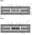
- FIG. 1 shows a schematic representation of the modulatable infrared emitter 1 in cross section.
- This is housed in a housing 15 , which consists of a lower support 17, side parts 21 and a cover element 19 .
- Sealing elements 23 can be present between the carrier 17, the cover element 19 and the side parts 21 .
- These sealing elements 23 are used to reduce a thermal exchange of the inside of the emitter 1, in which the MEMS heating element 3 is present, with the outside environment of the IR emitter 1.
- the MEMS heating element 3 inside the housing 15 consists of a spring structure 13 with individual, parallel, heatable regions 7.
- the projections of the heatable regions oriented in the direction of the cover element 19 and in the emission direction form the emission surface 10, which in turn form the total surface 9 with the non-heatable regions 11 in between.
- An enlargement of the total area 9 of the MEMS heating element 3 of the relative movement between the heating element 3 and the screen structure 3 is realized by two actuators 5 in the form of comb drives which are placed laterally from the heating element 3 and which is directly coupled to the spring structure 13 of the MEMS heating element 3 .
- the actuators 5 are in turn attached to a side part 21 of the housing 15 .
- the MEMS heating element 3 is free-standing except for the connection to the actuators 5 .
- Figure 2 shows the modulatable infrared emitter 1 Figure 1 in a second state, in which the ratio of the emission area 10 to the total area 9 is maximum, since the spring structure 13 is in a compressed state by the actuators 5 , in which the area of the non-heatable regions 11 is minimized and thus also the total area 9, which is composed of the emission surface 10 and the non-heatable regions 11 .
- the emission surface 10 remains unchanged.
- the ratio between emission area 10 and total area 9 is maximum in the second state. This also applies to the intensity of the emitted infrared radiation.
- Figure 3 shows the modulatable infrared emitter 1 from the Figures 1 and 2 in a first state in which the emitted radiation has a minimal intensity.
- the spring structure 13 is brought into an extended state by the actuators 5 , in which the area of the non-heatable regions 11 is maximized while the emission area 10 remains the same.
- the total area 9 is therefore also maximized , so that the ratio of the emission area 10 to the total area of the MEMS heating element is minimal and at least a factor 2 less than in the second state.
- the intensity of the infrared radiation emitted is also minimal in this state.
- FIG 4 shows an alternative embodiment of the modulatable IR emitter 1, in which the MEMS heating element 3 has an interlocking structure 25 instead of the spring structure.
- the interlocking structure 25 can be compressed by the actuators 5 , which corresponds to a second state or can be pulled apart, which corresponds to a second state.
- the interlocking structure 25 is formed by a plurality of T-pieces, which are arranged alternately upwards or downwards and thus fit into one another in a compressed, second state for the smallest possible total area 9 .
- the heatable regions 7 can preferably be formed by the upper T-pieces, the transverse bars of which preferably coincide essentially with the emission surface 10 .
- the individual T-pieces of the structure can preferably be connected to one another by an elastic structure.
- Figure 5 shows a further embodiment of the modulatable IR emitter 1, the MEMS heating element 3 having a lamella structure 27 with rotatable lamellae.
- the fins form the heatable regions 7 and are rotatably mounted in a frame structure 31 .
- a second state is shown in which heatable regions 7, emission surface 10 and total surface 9 essentially coincide.
- the ratio of the emission area 10 to the total area of the MEMS heating element and the intensity in the emission direction 29 is at a maximum.
- Figure 6 shows the same embodiment of the modulatable infrared emitter 1 in a first state.
- the individual fins are rotated by 90 ° with respect to the emission direction, preferably by means of an actuator, so that the heatable regions 7 likewise no longer point in this direction.
- the emission area 10 becomes minimal, the total area 9 is now essentially identical to the non-heatable areas 11.
- the ratio of the emission area 10 to the total area of the MEMS heating element is minimal, as is the intensity in the emission direction. It is also implemented in this way that the ratio of the emission area 10 to the total area of the MEMS heating element in the first state is at least a factor 2 less than in the second state.
Landscapes
- Physics & Mathematics (AREA)
- Spectroscopy & Molecular Physics (AREA)
- General Physics & Mathematics (AREA)
- Chemical & Material Sciences (AREA)
- Life Sciences & Earth Sciences (AREA)
- Analytical Chemistry (AREA)
- Biochemistry (AREA)
- General Health & Medical Sciences (AREA)
- Health & Medical Sciences (AREA)
- Immunology (AREA)
- Pathology (AREA)
- Engineering & Computer Science (AREA)
- Computer Hardware Design (AREA)
- Microelectronics & Electronic Packaging (AREA)
- Micromachines (AREA)
- Investigating Or Analysing Materials By Optical Means (AREA)
Priority Applications (8)
| Application Number | Priority Date | Filing Date | Title |
|---|---|---|---|
| EP18194206.1A EP3623780A1 (fr) | 2018-09-13 | 2018-09-13 | Modulation de l'intensité de rayonnement d'un émetteur ir au moyen de la variation de la surface d'émission |
| CA3111006A CA3111006C (fr) | 2018-09-13 | 2019-09-13 | Modulation de l'intensite de rayonnement d'un emetteur a infrarouge en modifiant la zone de rayonnement |
| EP19768822.9A EP3850318B1 (fr) | 2018-09-13 | 2019-09-13 | Modulation de l'intensité de rayonnement d'un émetteur ir au moyen de la variation de la surface d'émission |
| PCT/EP2019/074516 WO2020053402A1 (fr) | 2018-09-13 | 2019-09-13 | Modélisation de l'intensité de rayonnement d'un émetteur infrarouge par variation de la surface rayonnante |
| CN201980059574.7A CN112703378B (zh) | 2018-09-13 | 2019-09-13 | 通过辐射区域的变化来调制ir发射器的辐射强度 |
| KR1020217010854A KR102835256B1 (ko) | 2018-09-13 | 2019-09-13 | 방사 영역의 변화에 따른 ir 이미터의 방사 강도 조절 |
| US17/250,852 US11879784B2 (en) | 2018-09-13 | 2019-09-13 | Modeling the emission intensity of an IR emitter by varying the emission surface |
| JP2021513813A JP2022500637A (ja) | 2018-09-13 | 2019-09-13 | 表面の変化によるir放出器の放出強度の変調 |
Applications Claiming Priority (1)
| Application Number | Priority Date | Filing Date | Title |
|---|---|---|---|
| EP18194206.1A EP3623780A1 (fr) | 2018-09-13 | 2018-09-13 | Modulation de l'intensité de rayonnement d'un émetteur ir au moyen de la variation de la surface d'émission |
Publications (1)
| Publication Number | Publication Date |
|---|---|
| EP3623780A1 true EP3623780A1 (fr) | 2020-03-18 |
Family
ID=63642532
Family Applications (2)
| Application Number | Title | Priority Date | Filing Date |
|---|---|---|---|
| EP18194206.1A Withdrawn EP3623780A1 (fr) | 2018-09-13 | 2018-09-13 | Modulation de l'intensité de rayonnement d'un émetteur ir au moyen de la variation de la surface d'émission |
| EP19768822.9A Active EP3850318B1 (fr) | 2018-09-13 | 2019-09-13 | Modulation de l'intensité de rayonnement d'un émetteur ir au moyen de la variation de la surface d'émission |
Family Applications After (1)
| Application Number | Title | Priority Date | Filing Date |
|---|---|---|---|
| EP19768822.9A Active EP3850318B1 (fr) | 2018-09-13 | 2019-09-13 | Modulation de l'intensité de rayonnement d'un émetteur ir au moyen de la variation de la surface d'émission |
Country Status (6)
| Country | Link |
|---|---|
| US (1) | US11879784B2 (fr) |
| EP (2) | EP3623780A1 (fr) |
| JP (1) | JP2022500637A (fr) |
| KR (1) | KR102835256B1 (fr) |
| CN (1) | CN112703378B (fr) |
| WO (1) | WO2020053402A1 (fr) |
Families Citing this family (6)
| Publication number | Priority date | Publication date | Assignee | Title |
|---|---|---|---|---|
| EP3717465B1 (fr) | 2017-11-30 | 2026-01-21 | Step Pharma S.A.S. | Composés |
| EP3623780A1 (fr) * | 2018-09-13 | 2020-03-18 | Hahn-Schickard-Gesellschaft für angewandte Forschung e.V. | Modulation de l'intensité de rayonnement d'un émetteur ir au moyen de la variation de la surface d'émission |
| CN213280087U (zh) * | 2019-12-10 | 2021-05-25 | 楼氏电子(苏州)有限公司 | 力反馈致动器和微机电系统电容换能器 |
| CN115200730A (zh) * | 2021-03-25 | 2022-10-18 | 威卡亚力山大维甘德欧洲两合公司 | 温度传感器 |
| CN113281916B (zh) * | 2021-05-10 | 2023-06-30 | 清华大学 | 连续调节物体红外发射率的方法和基于此的红外功能表面 |
| CN116232457B (zh) * | 2023-05-06 | 2023-07-28 | 武汉工程大学 | 可调制发射率的红外发射器及红外发射器系统 |
Citations (4)
| Publication number | Priority date | Publication date | Assignee | Title |
|---|---|---|---|---|
| WO2007070540A2 (fr) * | 2005-12-12 | 2007-06-21 | Irina Puscasu | Appareil absorbeur-emetteur de film mince et procedes |
| US20090244678A1 (en) * | 2005-02-23 | 2009-10-01 | Pixtronix, Inc. | Display apparatus and methods for manufacture thereof |
| WO2017060264A2 (fr) * | 2015-10-05 | 2017-04-13 | Sintef Tto As | Source de rayonnement infrarouge |
| DE102017206183A1 (de) | 2016-04-13 | 2017-10-19 | Infineon Technologies Dresden Gmbh | System und Verfahren für eine Kammantrieb-MEMS-Vorrichtung |
Family Cites Families (11)
| Publication number | Priority date | Publication date | Assignee | Title |
|---|---|---|---|---|
| NO149679C (no) * | 1982-02-22 | 1984-05-30 | Nordal Per Erik | Anordning ved infraroed straalingskilde |
| US7129519B2 (en) * | 2002-05-08 | 2006-10-31 | Advanced Technology Materials, Inc. | Monitoring system comprising infrared thermopile detector |
| KR100452946B1 (ko) * | 2002-11-26 | 2004-10-14 | 한국전자통신연구원 | 저전력형 미세 열순환 소자 및 그 제조 방법 |
| WO2007141826A1 (fr) * | 2006-05-26 | 2007-12-13 | Nalux Co., Ltd. | Source de lumière infrarouge |
| CN101949836B (zh) * | 2010-08-25 | 2011-11-30 | 华中科技大学 | 一种热辐射红外发射和探测集成器件 |
| CN103332648A (zh) * | 2013-04-10 | 2013-10-02 | 南京曼莫斯电子科技有限公司 | 电调制mems 红外光源及其制备方法 |
| CN105004694A (zh) * | 2015-05-29 | 2015-10-28 | 苏州诺联芯电子科技有限公司 | 基于mems技术的阵列式红外光源器件及其制备方法 |
| US10347814B2 (en) * | 2016-04-01 | 2019-07-09 | Infineon Technologies Ag | MEMS heater or emitter structure for fast heating and cooling cycles |
| FR3055738B1 (fr) * | 2016-09-05 | 2018-09-07 | Commissariat A L'energie Atomique Et Aux Energies Alternatives | Surface d'emission de rayonnement infrarouge ir a emissivite thermique elevee et a grande duree de vie et son procede de fabrication |
| US20190259108A1 (en) * | 2018-02-20 | 2019-08-22 | Osram Gmbh | Controlled Agricultural Systems and Methods of Managing Agricultural Systems |
| EP3623780A1 (fr) * | 2018-09-13 | 2020-03-18 | Hahn-Schickard-Gesellschaft für angewandte Forschung e.V. | Modulation de l'intensité de rayonnement d'un émetteur ir au moyen de la variation de la surface d'émission |
-
2018
- 2018-09-13 EP EP18194206.1A patent/EP3623780A1/fr not_active Withdrawn
-
2019
- 2019-09-13 WO PCT/EP2019/074516 patent/WO2020053402A1/fr not_active Ceased
- 2019-09-13 KR KR1020217010854A patent/KR102835256B1/ko active Active
- 2019-09-13 CN CN201980059574.7A patent/CN112703378B/zh active Active
- 2019-09-13 US US17/250,852 patent/US11879784B2/en active Active
- 2019-09-13 JP JP2021513813A patent/JP2022500637A/ja active Pending
- 2019-09-13 EP EP19768822.9A patent/EP3850318B1/fr active Active
Patent Citations (4)
| Publication number | Priority date | Publication date | Assignee | Title |
|---|---|---|---|---|
| US20090244678A1 (en) * | 2005-02-23 | 2009-10-01 | Pixtronix, Inc. | Display apparatus and methods for manufacture thereof |
| WO2007070540A2 (fr) * | 2005-12-12 | 2007-06-21 | Irina Puscasu | Appareil absorbeur-emetteur de film mince et procedes |
| WO2017060264A2 (fr) * | 2015-10-05 | 2017-04-13 | Sintef Tto As | Source de rayonnement infrarouge |
| DE102017206183A1 (de) | 2016-04-13 | 2017-10-19 | Infineon Technologies Dresden Gmbh | System und Verfahren für eine Kammantrieb-MEMS-Vorrichtung |
Non-Patent Citations (1)
| Title |
|---|
| IRINA PUSCASU: "Photonic crystals enable infrared gas sensors", PROCEEDINGS OF SPIE, vol. 5515, 1 January 2004 (2004-01-01), pages 58 - 66, XP055011700, ISSN: 0277-786X, DOI: 10.1117/12.559644 * |
Also Published As
| Publication number | Publication date |
|---|---|
| CN112703378B (zh) | 2024-05-17 |
| CA3111006A1 (fr) | 2020-03-19 |
| EP3850318A1 (fr) | 2021-07-21 |
| US20220042852A1 (en) | 2022-02-10 |
| JP2022500637A (ja) | 2022-01-04 |
| US11879784B2 (en) | 2024-01-23 |
| CN112703378A (zh) | 2021-04-23 |
| KR20210053339A (ko) | 2021-05-11 |
| EP3850318B1 (fr) | 2022-11-16 |
| KR102835256B1 (ko) | 2025-07-16 |
| WO2020053402A1 (fr) | 2020-03-19 |
Similar Documents
| Publication | Publication Date | Title |
|---|---|---|
| EP3850318B1 (fr) | Modulation de l'intensité de rayonnement d'un émetteur ir au moyen de la variation de la surface d'émission | |
| EP3924702B1 (fr) | Émetteur ir à degré d'émission modulable à base de métamatériaux | |
| EP3850317B1 (fr) | Modulation d'un émetteur ir mobile à l'aide d'une structure de diaphragme | |
| DE69428928T2 (de) | Einkanal-Gaskonzentrationsmessvorrichtung | |
| DE69518386T2 (de) | Spektrometer | |
| DE69511488T2 (de) | Selektiver Infrarotdetektor | |
| DE102004044196B4 (de) | Massenspektrometer mit einem Lasersystem für die Ionisation einer Probe durch matrixunterstützte Laserdesorption in der massenspektrometrischen Analyse | |
| EP3786616A1 (fr) | Cellule photoacustique à base de mems | |
| DE2553378C2 (de) | Wärmestrahlungs-Abbildungsvorrichtung | |
| EP3702772A1 (fr) | Spectroscope photoacoustique doté d'une structure oscillante en tant que détecteur sonore | |
| EP3372988B1 (fr) | Procédé et dispositif de mesure d'une concentration de matière dans un milieu gazeux au moyen de la spectroscopie d'absorption | |
| DE102010031206B4 (de) | Abstimmbares Fabry-Pérot-Filter und Verfahren zu seiner Herstellung | |
| EP1825530B1 (fr) | Source de rayonnements tétrahertz cohérents | |
| DE102012103662B3 (de) | Dünnschicht-Infrarotstrahlungsquelle und Verfahren zu deren Herstellung | |
| EP2562784B1 (fr) | Agencement de capteur destiné à caractériser les processus de revêtement par plasma, gravure par plasma et traitement plasma ainsi que le procédé de détermination de grandeurs de référence dans ces processus | |
| WO2021224213A1 (fr) | Détecteur de rayonnement micromécanique, spectromètre micromécanique et procédé de mesure de rayonnement | |
| DE102013008486B4 (de) | Rauscharmes optisches Element zur Detektion von Strahlung mittels Messung elektrischer Signale und Verwendung desselben zur Einstellung einer Reflexionsbedingung | |
| DE102013013239B4 (de) | Adaptiver optischer Filter bzw. spektral einstellbare Lichtquelle | |
| DE2542362C3 (de) | Ionenstreuspektroskopisches Verfahren und Vorrichtung zur Durchführung desselben | |
| DE102018128983B4 (de) | Verfahren zur Temperaturbestimmung sowie zugehöriges Spektral-Reflexionsmesssystem | |
| DE102019002329A1 (de) | Verfahren zur kontrollierten Abdünnung eines mehrlagigen van-der-Waals Schichtsystems | |
| DE10339709A1 (de) | Verfahren und Vorrichtung zur Messung lokaler und momentaner Temperatur in einem gasförmigen Fluid | |
| DE102016107501B3 (de) | Wellenlängenmessvorrichtung und Verfahren zur Messung der Wellenlänge | |
| DE10102261C1 (de) | Einrichtung zur Strahlführung von einer Szene über ein Interferometer zu einem Detektor für ein abbildendes und/oder nicht abbildendes Fourier-Transform Spektrometer sowie Verfahren zur Optimierung dieser Einrichtung | |
| WO2025082951A1 (fr) | Microphone mems ayant une ouverture de ventilation |
Legal Events
| Date | Code | Title | Description |
|---|---|---|---|
| PUAI | Public reference made under article 153(3) epc to a published international application that has entered the european phase |
Free format text: ORIGINAL CODE: 0009012 |
|
| STAA | Information on the status of an ep patent application or granted ep patent |
Free format text: STATUS: THE APPLICATION HAS BEEN PUBLISHED |
|
| AK | Designated contracting states |
Kind code of ref document: A1 Designated state(s): AL AT BE BG CH CY CZ DE DK EE ES FI FR GB GR HR HU IE IS IT LI LT LU LV MC MK MT NL NO PL PT RO RS SE SI SK SM TR |
|
| AX | Request for extension of the european patent |
Extension state: BA ME |
|
| STAA | Information on the status of an ep patent application or granted ep patent |
Free format text: STATUS: THE APPLICATION IS DEEMED TO BE WITHDRAWN |
|
| 18D | Application deemed to be withdrawn |
Effective date: 20200919 |