EP3624100B1 - Circuit de commande d'émission de lumière, pilote de commande d'émission de lumière et dispositif d'affichage - Google Patents
Circuit de commande d'émission de lumière, pilote de commande d'émission de lumière et dispositif d'affichage Download PDFInfo
- Publication number
- EP3624100B1 EP3624100B1 EP18901277.6A EP18901277A EP3624100B1 EP 3624100 B1 EP3624100 B1 EP 3624100B1 EP 18901277 A EP18901277 A EP 18901277A EP 3624100 B1 EP3624100 B1 EP 3624100B1
- Authority
- EP
- European Patent Office
- Prior art keywords
- thin film
- film transistor
- emission control
- clock signal
- signal
- Prior art date
- Legal status (The legal status is an assumption and is not a legal conclusion. Google has not performed a legal analysis and makes no representation as to the accuracy of the status listed.)
- Active
Links
Images


Classifications
-
- G—PHYSICS
- G09—EDUCATION; CRYPTOGRAPHY; DISPLAY; ADVERTISING; SEALS
- G09G—ARRANGEMENTS OR CIRCUITS FOR CONTROL OF INDICATING DEVICES USING STATIC MEANS TO PRESENT VARIABLE INFORMATION
- G09G3/00—Control arrangements or circuits, of interest only in connection with visual indicators other than cathode-ray tubes
- G09G3/20—Control arrangements or circuits, of interest only in connection with visual indicators other than cathode-ray tubes for presentation of an assembly of a number of characters, e.g. a page, by composing the assembly by combination of individual elements arranged in a matrix no fixed position being assigned to or needed to be assigned to the individual characters or partial characters
- G09G3/22—Control arrangements or circuits, of interest only in connection with visual indicators other than cathode-ray tubes for presentation of an assembly of a number of characters, e.g. a page, by composing the assembly by combination of individual elements arranged in a matrix no fixed position being assigned to or needed to be assigned to the individual characters or partial characters using controlled light sources
- G09G3/30—Control arrangements or circuits, of interest only in connection with visual indicators other than cathode-ray tubes for presentation of an assembly of a number of characters, e.g. a page, by composing the assembly by combination of individual elements arranged in a matrix no fixed position being assigned to or needed to be assigned to the individual characters or partial characters using controlled light sources using electroluminescent panels
- G09G3/32—Control arrangements or circuits, of interest only in connection with visual indicators other than cathode-ray tubes for presentation of an assembly of a number of characters, e.g. a page, by composing the assembly by combination of individual elements arranged in a matrix no fixed position being assigned to or needed to be assigned to the individual characters or partial characters using controlled light sources using electroluminescent panels semiconductive, e.g. using light-emitting diodes [LED]
- G09G3/3208—Control arrangements or circuits, of interest only in connection with visual indicators other than cathode-ray tubes for presentation of an assembly of a number of characters, e.g. a page, by composing the assembly by combination of individual elements arranged in a matrix no fixed position being assigned to or needed to be assigned to the individual characters or partial characters using controlled light sources using electroluminescent panels semiconductive, e.g. using light-emitting diodes [LED] organic, e.g. using organic light-emitting diodes [OLED]
- G09G3/3266—Details of drivers for scan electrodes
-
- G—PHYSICS
- G09—EDUCATION; CRYPTOGRAPHY; DISPLAY; ADVERTISING; SEALS
- G09G—ARRANGEMENTS OR CIRCUITS FOR CONTROL OF INDICATING DEVICES USING STATIC MEANS TO PRESENT VARIABLE INFORMATION
- G09G3/00—Control arrangements or circuits, of interest only in connection with visual indicators other than cathode-ray tubes
- G09G3/20—Control arrangements or circuits, of interest only in connection with visual indicators other than cathode-ray tubes for presentation of an assembly of a number of characters, e.g. a page, by composing the assembly by combination of individual elements arranged in a matrix no fixed position being assigned to or needed to be assigned to the individual characters or partial characters
- G09G3/22—Control arrangements or circuits, of interest only in connection with visual indicators other than cathode-ray tubes for presentation of an assembly of a number of characters, e.g. a page, by composing the assembly by combination of individual elements arranged in a matrix no fixed position being assigned to or needed to be assigned to the individual characters or partial characters using controlled light sources
- G09G3/30—Control arrangements or circuits, of interest only in connection with visual indicators other than cathode-ray tubes for presentation of an assembly of a number of characters, e.g. a page, by composing the assembly by combination of individual elements arranged in a matrix no fixed position being assigned to or needed to be assigned to the individual characters or partial characters using controlled light sources using electroluminescent panels
- G09G3/32—Control arrangements or circuits, of interest only in connection with visual indicators other than cathode-ray tubes for presentation of an assembly of a number of characters, e.g. a page, by composing the assembly by combination of individual elements arranged in a matrix no fixed position being assigned to or needed to be assigned to the individual characters or partial characters using controlled light sources using electroluminescent panels semiconductive, e.g. using light-emitting diodes [LED]
-
- G—PHYSICS
- G09—EDUCATION; CRYPTOGRAPHY; DISPLAY; ADVERTISING; SEALS
- G09G—ARRANGEMENTS OR CIRCUITS FOR CONTROL OF INDICATING DEVICES USING STATIC MEANS TO PRESENT VARIABLE INFORMATION
- G09G3/00—Control arrangements or circuits, of interest only in connection with visual indicators other than cathode-ray tubes
- G09G3/20—Control arrangements or circuits, of interest only in connection with visual indicators other than cathode-ray tubes for presentation of an assembly of a number of characters, e.g. a page, by composing the assembly by combination of individual elements arranged in a matrix no fixed position being assigned to or needed to be assigned to the individual characters or partial characters
- G09G3/34—Control arrangements or circuits, of interest only in connection with visual indicators other than cathode-ray tubes for presentation of an assembly of a number of characters, e.g. a page, by composing the assembly by combination of individual elements arranged in a matrix no fixed position being assigned to or needed to be assigned to the individual characters or partial characters by control of light from an independent source
-
- G—PHYSICS
- G11—INFORMATION STORAGE
- G11C—STATIC STORES
- G11C19/00—Digital stores in which the information is moved stepwise, e.g. shift registers
- G11C19/28—Digital stores in which the information is moved stepwise, e.g. shift registers using semiconductor elements
-
- G—PHYSICS
- G09—EDUCATION; CRYPTOGRAPHY; DISPLAY; ADVERTISING; SEALS
- G09G—ARRANGEMENTS OR CIRCUITS FOR CONTROL OF INDICATING DEVICES USING STATIC MEANS TO PRESENT VARIABLE INFORMATION
- G09G2310/00—Command of the display device
- G09G2310/02—Addressing, scanning or driving the display screen or processing steps related thereto
- G09G2310/0264—Details of driving circuits
- G09G2310/0286—Details of a shift registers arranged for use in a driving circuit
Definitions
- Embodiments of the present application relate to the field of display technologies, and more specifically to an emission control circuit, an emission control driver and a display device.
- a display device may include a plurality of pixels, a data driver, a scan driver, and an emission control driver.
- the plurality of pixels are configured to display an image
- the data driver is configured to provide data voltages to the pixels
- the scan driver is configured to provide scanning signals to the pixels
- the emission control driver is configured to provide emission control signals to the pixels
- the emission control signals may control emission time of the pixels.
- the emission control driver may include multiple-stages of emission control circuits, each of which may be configured to control emission time of a row of the pixels.
- one stage of emission control circuit which may include a plurality of thin film transistors, an initial signal, and a plurality of clock signals, may control the thin film transistors to be in on-state or off-state, so that the emission control circuit can output the emission control signals.
- each stage of the emission control circuit includes a large number of thin film transistors (usually more than 20), resulting in a complicated emission control circuit.
- US 2014/0055444 A1 provides an emission control driver which includes stages sequentially out-putting emission control signals through emission controllines. Each stage incledes a first signal processor, a second signal processor and a third signal processor. And the third signal processor includes eighth, ninth, and tenth transistors M8, M9, and M10 and a third capacitor C3.
- US 2017/0301295 A1 provides an emission control driver which includes a plurality of stages configured to output a plurality of emission control signals, respectively. Each stage includes a plurality of transistors and capacitors.
- an emission control circuit is provided in embodiments of the present application, and the circuit includes less thin film transistors and has a simple structure, to achieve requirements of simplifying a structure of the emitting control circuit.
- the emission control signal output by the emission control circuit may control pixels to emit light, and the circuit structure of the emission control circuit is relatively simple compared to the prior art.
- a first thin film transistor, a second thin film transistor, a third thin film transistor, a fourth thin film transistor, a fifth thin film transistor, a sixth thin film transistor, a seventh thin film transistor, an eighth thin film transistor, a ninth thin film transistor, and a tenth thin film transistor may all be N-type thin film transistors, or may all be P-type thin film transistors.
- at least one of the transistors may be a N-type thin film transistor, and the rest of the transistors are P-type thin film transistors, which is not specifically limited herein.
- FIG. 1 is a schematic structural diagram of an emission control circuit according to an embodiment of the present application.
- the emission control circuit can generate an emission control signal that can control emission time of pixels.
- the emission control circuit is described below.
- the emission control circuit may include: a first control unit 11, a second control unit 12, and an emission control unit 13.
- An input terminal of the first control unit 11 may be respectively connected to an initial signal line, a first clock signal line, and a first power source VGL.
- the initial signal line may provide an initial signal EIN
- the first clock signal line may provide a first clock signal CK1.
- the first clock signal CK1 may be a pulse signal
- the first power source VGL may have a negative voltage, i.e. the first power source VGL may output a low level.
- the first control unit 11 may be configured to output a first control signal under control of the initial signal EIN, the first clock signal CK1, and the first power source VGL.
- An input terminal of the second control unit 12 may be respectively connected to the first control unit 11, a second clock signal line, and a second power source VGH.
- the second clock signal line may provide a second clock signal CK2, and the second clock signal CK2 may also be a pulse signal.
- the second power source VGH may have a positive voltage, i.e. the second power source VGH may output a high level.
- the second control unit 12 may be configured to output a second control signal under control of the first control unit 11, the second clock signal CK2, and the second power source VGH.
- An input terminal of the emission control unit 13 may be respectively connected to the first control unit 11, the second control unit 12, the first power source VGL and the second power source VGH.
- the first control signal and the second control signal may be input to the emission control unit 13, and the emission control unit 13 may be configured to output an emission control signal EM under control of the first control signal and the second control signal.
- the emission control unit may output the emission control signal under control of the first control unit, the second control unit, the clock signal, and the voltage of the power source; and the emission control signal may control the emission time of the pixels.
- the emission control unit 13 may include: a ninth thin film transistor M9, a tenth thin film transistor M10, a second capacitor C2, and a third capacitor C3.
- a source of the ninth thin film transistor M9 is connected to the second power source VGH, a drain of the ninth thin film transistor M9 is connected to a source of the tenth thin film transistor M10, and a gate of the ninth thin film transistor M9 is connected to the output terminal, configured to output the second control signal, of the second control unit 12.
- a drain of the tenth thin film transistor M10 is connected to the first power source VGL, and a gate of the tenth thin film transistor M10 is connected to the output terminal, configured to output the first control signal, of the first control unit 11.
- a terminal of the second capacitor C2 is connected to the output terminal, configured to output the second control signal, of the second control unit 12, and another terminal of the second capacitor C2 is connected to the second power source VGH.
- a terminal of the third capacitor C3 is connected to the second clock signal CK2, and another terminal of the third capacitor C3 is connected to the output terminal, configured to output the first control signal, of the first control unit 11.
- the drain of the ninth thin film transistor M9 or the source of the tenth thin film transistor M10 is the output terminal of the emission control unit 13, and a signal output by the drain of the ninth thin film transistor M9 or the source of the tenth thin film transistor M10 is the emission control signal.
- the first control unit 11 shown in FIG. 1 may include: a first thin film transistor, a second thin film transistor, and a third thin film transistor.
- the second control unit 12 shown in FIG. 1 may include: a fourth thin film transistor, a fifth thin film transistor, a sixth thin film transistor, a seventh thin film transistor, an eighth thin film transistor, and a capacitor.
- FIG. 2 is a schematic structural diagram of an emission control circuit according to another embodiment of the present application.
- the first control unit 11 includes a first thin film transistor M1, a second thin film transistor M2, and a third thin film transistor M3.
- the second control unit 12 includes a fourth thin film transistor M4, a fifth thin film transistor M5, a sixth thin film transistor M6, a seventh thin film transistor M7, an eighth thin film transistor M8, and a first capacitor CI.
- the emission control unit 13 includes a ninth thin film transistor M9, a tenth thin film transistor M10, a second capacitor C2, and a third capacitor C3.
- the thin film transistors, shown in FIG. 2 are all P-type thin film transistors.
- the circuit structure of the emission control circuit shown in FIG. 2 is as follows.
- a gate of the first thin film transistor M1 is respectively connected to a source of the second thin film transistor M2, a gate of the third thin film transistor M3, and the first clock signal line; a drain of the first thin film transistor M1 is connected to the initial signal line; and a source of the first thin film transistor M1 is respectively connected to a gate of the second thin film transistor M2, a drain of the fifth thin film transistor M5, a gate of the eighth thin film transistor M8, a gate of the tenth thin film transistor M10, and one terminal of the third capacitor C3 (a first node N1 shown in FIG. 2 ).
- a drain of the second thin film transistor M2 is connected to a source of the third thin film transistor M3.
- a drain of the third thin film transistor M3 is connected to the first power source VGL.
- a gate of the fourth thin film transistor M4 is respectively connected to a gate of the sixth thin film transistor M6 and one terminal of the first capacitor C1 (a second node N2 shown in FIG. 2 ), and a source of the fourth thin film transistor M4 is connected to a source of the fifth thin film M5, and a drain of the fourth thin film transistor M4 is respectively connected to a drain of the eighth thin film transistor M8 and the second power source VGH.
- a gate of the fifth thin film transistor M5 is respectively connected to the second clock signal line, a drain of the sixth thin film transistor M6, a gate of the seventh thin film transistor M7, another terminal of the first capacitor C1, and another terminal of the third capacitor C3.
- a source of the sixth thin film transistor M6 is connected to a source of the seventh thin film transistor M7.
- a drain of the seventh thin film transistor M7 is respectively connected to a source of the eighth thin film transistor M8, a gate of the ninth thin film transistor M9, and a terminal of the second capacitor C2 (a third node N3 shown in FIG. 2 ).
- a source of the ninth thin film transistor M9 is respectively connected to the second power source VGH and another terminal of the second capacitor C2, and a drain of the ninth thin film transistor M9 is connected to a source of the tenth thin film transistor M10.
- a drain of the tenth thin film transistor M10 is connected to the first power source VGL.
- a signal output by the source of the first thin film transistor M1 (i.e., the first node N1 shown in FIG. 2 ) may be regarded as the first control signal;
- a signal output by the source of the eighth thin film transistor M8 (i.e., the third node N3 shown in FIG. 2 ) may be regarded as the second control signal;
- a signal output by the drain of the ninth thin film transistor M9 (or the source of the tenth thin film transistor M10) may be regarded as the emission control signal EM.
- the first control signal may be output to the gate of the tenth thin film transistor M10 and the tenth thin film transistor M10 is controlled by the first control signal to be in on-state or off-state; the second control signal may be output to the gate of the ninth thin film transistor M9 and the ninth thin film transistor M9 is controlled by the second control signal to be in on-state or off-state.
- the emission control signal EM may be output to pixels and the emission control signal EM is configured to control emission time of the pixels.
- first thin film transistor M1 the second thin film transistor M2, the third thin film transistor M3, the fourth thin film transistor M4, the fifth thin film transistor M5, the sixth thin film transistor M6, the seventh thin film transistor M7, the eighth thin film transistor M8, the ninth thin film transistor M9 and the tenth thin film transistor M10, may be selected according to a practical application.
- the first thin film transistor M1, the second thin film transistor M2, the third thin film transistor M3, the fourth thin film transistor M4, the fifth thin film transistor M5, the sixth thin film transistor M6, the seventh thin film transistor M7, the eighth thin film transistor M8, the ninth thin film transistor M9 and the tenth thin film transistor M10 may all be the P-type thin film transistor as described above; or at least one thin film transistor of the first thin film transistor M1, the second thin film transistor M2, the third thin film transistor M3, the fourth thin film transistor M4, the fifth thin film transistor M5, the sixth thin film transistor M6, the seventh thin film transistor M7, the eighth thin film transistor M8, the ninth thin film transistor M9 and the tenth thin film transistor M10 is an N-type thin film transistor.
- the first capacitor C1 and the third capacitor C3 may be bootstrap capacitors configured to raise or lower a level of a node, and the second capacitor C2 may be a storage capacitor configured to maintain the level of the node. This embodiment is described more specifically below.
- One terminal of the first capacitor C1 (i.e., the second node N2 shown in FIG. 2 ) is respectively connected to the gate of the fourth thin film transistor M4 and the gate of the sixth thin film transistor M6, and another terminal of the first capacitor C1 is connected to the second clock signal line.
- the first capacitor C1 may be configured to raise or lower a level of the second node N2, and thereby the fourth thin film transistor M4 and the sixth thin film transistor M6 are controlled to be in on-state or off-state.
- One terminal of the second capacitor C2 (i.e., the third node N3 shown in FIG. 2 ) is respectively connected to the source of the eighth thin film transistor M8 and the gate of the ninth thin film transistor M9, and another terminal of the second capacitor C2 is connected to the second power source VGH.
- the eighth thin film transistor M8 is in on-state, a voltage of the third node N3 is a high level, and when the eighth thin film transistor M8 is turned from being in on-state to being in off-state, since the second capacitor C2 is the storage capacitor, the second capacitor C2 may be configured to keep the high level of the third node N3 unchanged, and thereby the ninth thin film transistor M9 is controlled to remain being in off-state.
- One terminal of the third capacitor C3 (i.e., the first node N1 shown in FIG. 2 ) is respectively connected to the gate of the second thin film transistor M2, the gate of the eighth thin film transistor M8, and the gate of the tenth thin film transistor M10, and another terminal of the third capacitor C3 is connected to the second clock signal line.
- the third capacitor C3 may be configured to raise or pull down a voltage of the first node N1, and thereby the second thin film transistor M2, the eighth thin film transistor M8 and the tenth thin film transistor M10 are controlled to be in on-state or off-state.
- the third capacitor C3 another terminal of the third capacitor C3 is directly connected to the second clock signal line, and a delay of the second clock signal CK2 to the third capacitor C3 can be reduced, and the control efficiency of the third capacitor C3 to the second thin film transistor M2, the eighth thin film transistor M8, and the tenth thin film transistor M10 may be increased, so that a higher frequency emission control signal EM is output.
- the ninth thin film transistor M9 in order to ensure that the emission control circuit can output the emission control signal EM normally, when the tenth thin film transistor M10 is controlled by the first control signal to be in on-state, the ninth thin film transistor M9 may be controlled by the second control signal to be in off-state; or, when the tenth thin film transistor M10 is controlled by the first control signal to be in off-state, the ninth thin film transistor M9 may be controlled by the second control signal to be in on-state.
- the first power source VGL may be output to an EM end for the emission control signal through the tenth thin film transistor M10, i.e., the emission control unit outputs the first power source VGL;
- the second power source VGH may be output to an EM end for the emission control signal through the ninth thin film transistor M9, i.e., the emission control unit outputs the second power source VGH.
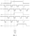
- FIG. 3 is a timing diagram of a driving method of the emission control circuit according to an embodiment of the present application.
- the timing diagram may be a timing diagram corresponding to a first stage of the emission control circuit in an emission control driver, and the timing diagram may be configured to drive the emission control circuit shown in FIG. 2 .
- EIN is an initial signal
- CK1 is a first clock signal
- CK2 is a second clock signal
- EM is an emission control signal.
- the first clock signal CK1 and the second clock signal CK2 have the same frequency
- the second clock signal CK2 has a delay time relative to the first clock signal CK1.
- the specific delay time is a time T, and the time T may be half of a period of the first clock signal CK1.
- Duration of the high level in the initial signal EIN may be twice the period of the first clock signal CK1.
- a duty period of the timing diagram shown in FIG. 3 may be divided into six phases: a first phase t1, a second phase t2, a third phase t3, a fourth phase t4, a fifth phase t5, and a sixth phase t6.
- the initial signal EIN has a low level
- the first clock signal CK1 has a low level
- the second clock signal CK2 has a high level.
- the first thin film transistor M1 and the third thin film transistor M3 are in on-state, and the initial signal EIN is applied to the first node N1 through the first thin film transistor M1, so that the first node N1 has a low level, and then the second thin film transistor M2, the eighth thin film transistor M8, and the tenth thin film transistor M10 are in on-state.
- the first clock signal CK1 is applied to the second node N2 through the second thin film transistor M2, and the first power source VGL is applied to the second node N2 through the third thin film transistor M3, so that the second node N2 has a low level, and then the forth thin film transistors M4 and the sixth thin film transistor M6 are in on-state.
- the fifth thin film transistor M5 and the seventh thin film transistor M7 are in off-state. Since the eighth thin film transistor M8 is in on-state, the second power source VGH is applied to the third node N3 through the eighth thin film transistor M8, so that the third node N3 has a high level, and then the ninth thin film transistor M9 is in off-state.
- the first power source VGL may be output by the tenth thin film transistor M10, so that the emission control signal EM has a low level.
- the initial signal EIN has a low level
- the first clock signal CK1 has a high level
- the second clock signal CK2 has a high level.
- the first thin film transistor M1 and the third thin film transistor M3 are in off-state.
- the first node N1 since the second clock signal CK2 at another terminal of the third capacitor C3 remains unchanged, the first node N1 will has the low level of the first phase t1, and then the second thin film transistor M2, the eighth thin film transistor M8, and the tenth thin film transistor M10 are still in on-state.
- the first clock signal CK1 is applied to the second node N2 through the second thin film transistor M2, so that the second node N2 has the high level and the fourth thin film transistor M4 and the sixth thin film transistor M6 are in off-state.
- the fifth thin film transistor M5 and the seventh thin film transistor M7 are still in off-state. Since the eighth thin film transistor M8 is in on-state, the third node N3 has the high level due to the second power source VGH, and then the ninth thin film transistor M9 is still in off-state.
- the first power source VGL may be output by the tenth thin film transistor M10, so that the emission control signal EM has a low level.
- the initial signal EIN has a low level
- the first clock signal CK1 has a high level
- the second clock signal CK2 has a low level, and then changed from the low level to a high level.
- the first thin film transistor M1 and the third thin film transistor M3 are in off-state.
- the second clock signal CK2 has the low level
- the fifth thin film transistor M5 and the seventh thin film transistor M7 are in on-state, and because of a bootstrap effect of the third capacitor C3, the voltage of the first node N1 is lowered and the voltage of the first node N1 is lower than the voltage of the first node N1 in the second phase t2, and then the second thin film transistor M2, the eighth thin film transistor M8, and the tenth thin film transistor M10 are in on-state.
- the first clock signal CK1 is applied to the second node N2 through the second thin film transistor M2, so that the second node N2 still has the high level and then the fourth thin film transistor M4 and the sixth thin film transistor M6 are in off-state. Since the eighth thin film transistor M8 is in on-state, and the voltage of the second power source VGH is applied to the third node N3 through the eighth thin film transistor M8, so that the third node N3 still has the high level, and then the ninth thin film transistor M9 is in off-state.
- the ninth thin film transistor M9 is in off-state and the tenth thin film transistor M10 is in on-state, the first power source VGL may be output by the tenth thin film transistor M10, so that the emission control signal EM has a low level.
- the fifth thin film transistor M5 and the seventh thin film transistor M7 are in off-state.
- the voltage of the first node N1 rises, but the first node N1 still has the low level, and then due to the first node N1, the second thin film transistor M2, the eighth thin film transistor M8, and the tenth thin film transistor M10 are still in on-state.
- the first thin film transistor M1 and the third thin film transistor M3 are still in off-state, and the first clock signal CK1 is applied to the second node N2 through the second thin film transistor M2, so that the second node N2 has the high level and then the fourth thin film transistor M4 and the sixth thin film transistor M6 are in off-state.
- the second power source VGH is applied to the third node N3 through the eighth thin film transistor M8, so that the third node N3 has the high level and then the ninth thin film transistor M9 is still in off-state.
- the ninth thin film transistor M9 is still in off-state and the tenth thin film transistor M10 is still in on-state, the first power source VGL may be output by the tenth thin film transistor M10, so that the emission control signal EM has a low level.
- the emission control signal EM has a low level.
- the initial signal EIN has a high level
- the first clock signal CK1 has a low level
- the second clock signal CK2 has a high level
- the first thin film transistor M1 and the third thin film transistor M3 are in on-state, and the initial signal EIN is applied to the first node N1 through the first thin film transistor M1, so that the first node N1 has the high level and then the second thin film transistor M2, the eighth thin film transistor M8, and the tenth thin film transistor M10 are in off-state.
- the first power source VGL is applied to the second node N2 through the third thin film transistor M3, so that the second node N2 has the low level, the fourth thin film transistor M4 and the sixth thin film transistor M6 are in on-state.
- the fifth thin film transistor M5 and the seventh thin film transistor M7 are in off-state. Since the eighth thin film transistor M8 is in off-state, under a storage control of the second capacitor C2, the third node N3 still has the high level being same as the high level in the third phase t3, and the ninth thin film transistor M9 turns to be in off-state.
- the emission control signal EM still has the low level being same as the low level in the third phase t3.
- the first clock signal CK1 has the high level
- the first thin film transistor M1 and the third thin film transistor M3 are in off-state
- the first node N1 will still has the high level
- the second node N2 will keep the low level unchanged
- the third node N3 will keep the high level unchanged.
- the second thin film transistor M2, the eighth thin film transistor M8, and the tenth thin film transistor M10 are still in off-state
- the fourth thin film transistor M4 and the sixth thin film transistor M6 are still in on-state
- the ninth thin film transistor M9 is still in off-state. Due to the second clock signal CK2, the fifth thin film transistor M5 and the seventh thin film transistor M7 are in off-state.
- the emission control signal EM keeps the low level being same as the low level in the third phase t3.
- the emission control signal EM has a low level.
- the initial signal EIN has a high level
- the first clock signal CK1 has a high level, changed from the high level to a low level, and then changed from the low level to a high level
- the second clock signal CK2 has a low level, changed from the low level to a high level, changed from the high level to a low level, and then changed from the low level to a high level.
- the first thin film transistor M1 and the third thin film transistor M3 are in off-state, and the fifth thin film transistor M5 and the seventh thin film transistor M7 are in on-state.
- the second node N2 is lowered and the voltage of the second node N2 is lower than the voltage of the second node N2 of the fourth stage t4, and then the fourth thin film transistor M4 and the sixth thin film transistor M6 are in on-state.
- the second clock signal CK2 may act on the third node N3 through the sixth thin film transistor M6 and the seventh thin film transistor M7, so that the third node N3 has the low level and then the ninth thin film transistor M9 is in on-state.
- the fourth thin film transistor M4 and the fifth thin film transistor M5 are on, the second power source VGH is applied to the first node N1 through the fourth thin film transistor M4 and the fifth thin film transistor M5, so that the first node N1 has the high level and then the second thin film transistor M2, the eighth thin film transistor M8, and the tenth thin film transistor M10 are in off-state.
- the second power source VGH may be output by the ninth thin film transistor M9, so that the emission control signal EM has a high level.
- the first node N1 still keeps the high level unchanged
- the voltage of the third node N3 still keeps the low level unchanged.
- the first clock signal CK1 is changed from the high level to the low level and the second clock signal CK2 still has the high level
- the first Node N1 still keeps the high level unchanged
- the third node N3 still keeps the low level unchanged.
- the first clock signal CK1 is changed from the low level to the high level
- the second clock signal CK2 is changed from the high level to the low level, and then changed from the low level to the high level
- the first node N1 still keeps the high level unchanged
- the third node N3 still keeps the low level unchanged.
- the ninth thin film transistor M9 is in on-state
- the tenth thin film transistor M10 is in off-state
- the second power source VGH may be output by the ninth thin film transistor M9, so that the emission control signal EM has a high level.
- the initial signal EIN has a low level
- the first clock signal CK1 has a low level
- the second clock signal CK2 has a high level.
- a working principle of the emission control circuit may be referred to a working principle of the emission control circuit in the first phase t1 described above, and a description of the working principle is not repeated herein.
- the emission control signal EM has a low level.
- a waveform diagram of the emission control signal EM which is output by the emission control unit may be as shown in FIG. 3 .
- the emission control circuit shown in FIG. 2 includes ten thin film transistors and three capacitors. Compared with the emission control circuit in the prior art, the number of thin film transistors and the number of capacitors are small, and the circuit structure of the emission control circuit is relatively simple.
- FIG. 4 is a schematic structural diagram of an emission control driver according to an embodiment of the present application.
- the emission control driver may include at least two stages emission control circuit described in the first Embodiment.
- the emission control driver shown in FIG. 4 includes N stages of emission control circuits, which may include, respectively: an emission control circuit 1, an emission control circuit 2, an emission control circuit 3, ..., and an emission control circuit n.
- the emission control circuit 1 is a first stage emission control circuit
- the emission control circuit 2 is a second stage emission control circuit
- the emission control circuit 3 is a third stage emission control circuit, ...
- the emission control circuit n is a nth stage emission control circuit, n is an integer greater than 1.
- an input signal of the emission control circuit 1 is an initial signal EIN
- an emission control signal EM1 output by the emission control circuit 1 may be used as an initial signal of the emission control circuit 2
- the emission control signal output by the emission control circuit 2 may be used as an initial signal of the emission control circuit 3
- the emission control signal EM(n-1) output by the emission control circuit (n-1) may be used as an initial signal of the emission control circuit n
- n is the integer greater than 1.
- a first clock signal of the emission control circuit 1 may be used as a second clock signal of the emission control circuit 2, and the second clock signal of the emission control circuit 1 may be used as a first clock signal of the emission control circuit 2; the first clock of the emission control circuit 2 may be used as a second clock signal of the emission control circuit 3, and the second clock signal of the emission control circuit 2 may be used as a first clock signal of the emission control circuit 3, ..., and so on, the first clock signal of the emission control circuit (n-1) may be used as a second clock signal of the emission control circuit n, and the second clock signal of the emission control circuit (n-1) may be used as a first clock signal of the emission control circuit n, and n is the integer greater than 1.
- FIG. 5 is a timing diagram of the emission control driver according to an embodiment of the present application.
- EIN is an initial signal input to a first stage of an emission control circuit
- CK1-1 is a first clock signal input to the emission control circuit 1
- CK2-1 is a second clock signal input to the emission control circuit 1
- the emission control circuit 1 may output an emission control signal EM1 under control of the initial signal EIN, the first clock signal CK1-1, and the second clock signal CK2-1.
- the emission control signal EM1 may be used as an initial signal of an emission control circuit 2.
- CK1-2 is a first clock signal input to the emission control circuit 2
- CK2-2 is a second clock signal input to the emission control circuit 2
- the emission control circuit 2 may output an emission control signal EM2 under control of the initial signal EIN, the first clock signal CK1-2, and the second clock signal CK2-2.
- the first clock signal CK1-2 of the emission control circuit 2 is the same as the second clock signal CK2-1 of the emission control circuit 1
- the second clock signal CK2-2 of the emission control circuit 2 is the same as the first clock signal CK1-1 of the emission control circuit 1
- the emission control signal EM2 output from the emission control circuit 2 is delayed with respect to the emission control signal EM1 output from the emission control circuit 1.
- an emission control signal EM(n-1) output by an emission control circuit (n-1) may be used as an initial signal of an emission control circuit n, and CK1-n is a first clock signal input to the emission control circuit n, CK2-n is a second clock signal input to the emission control circuit n.
- the first clock signal CK1-n may be the same as the second clock signal CK2-1, the second clock signal CK2-n may be the same as the first clock signal CK1-1, and the emission control circuit n may output the emission control signal EMn under control of the initial signal EM(n-1), the first clock signal CK1-n, and the second clock signal CK2-n.
- the initial signal EM(n-1), the first clock signal CK1-n, and the second clock signal CK2-n are not shown in FIG. 5 .
- the embodiments of the present application further provide a display device, which may include an emission control driver as described above.
Landscapes
- Engineering & Computer Science (AREA)
- Physics & Mathematics (AREA)
- Computer Hardware Design (AREA)
- General Physics & Mathematics (AREA)
- Theoretical Computer Science (AREA)
- Control Of Indicators Other Than Cathode Ray Tubes (AREA)
- Shift Register Type Memory (AREA)
- Control Of El Displays (AREA)
- Electronic Switches (AREA)
- Electroluminescent Light Sources (AREA)
Claims (9)
- Circuit de commande d'émission, comprenant: une première unité de commande (11), une deuxième unité de commande (12) et une unité de commande d'émission (13),
dans lequel :la première unité de commande (11), dont une borne de sortie (N1) est conçue pour émettre un premier signal de commande, est respectivement reliée à une ligne de signal initial (EIN), à une première ligne de signal d'horloge (CK1) et à une première source d'alimentation (VGL) ;la deuxième unité de commande (12), dont une borne de sortie (N3) est conçue pour émettre un deuxième signal de commande, est respectivement reliée à la première unité de commande (11), à une deuxième ligne de signal d'horloge (CK2) et à une deuxième source d'alimentation (VGH) ; etl'unité de commande d'émission (13), dont une borne de sortie est conçue pour émettre un signal de commande d'émission sous la commande du premier signal de commande et du deuxième signal de commande, est respectivement reliée à la première unité de commande (11), à la deuxième unité de commande (12), à la première source d'alimentation (VGL) et à la deuxième source d'alimentation (VGH) ;ladite unité de commande d'émission (13) comprenant un neuvième transistor à couches minces (M9), un dixième transistor à couches minces (M10), un deuxième condensateur (C2), et un troisième condensateur (C3), étant entendu que :une source du neuvième transistor à couches minces (M9) est reliée à la deuxième source d'alimentation (VGH), un drain du neuvième transistor à couches minces (M9) est relié à une source du dixième transistor à couches minces (M10), et une grille du neuvième transistor à couches minces (M9) est reliée à la borne de sortie (N3), conçue pour émettre le deuxième signal de commande, de la deuxième unité de commande (12),un drain du dixième transistor à couches minces (M10) est relié à la première source d'alimentation (VGL), et une grille du dixième transistor à couches minces (M10) est reliée à la borne de sortie (N1), conçue pour émettre le premier signal de commande, de la première unité de commande (11),une borne du deuxième condensateur (C2) est reliée à la borne de sortie de la deuxième unité de commande (12) conçue pour émettre le deuxième signal de commande, et une autre borne du deuxième condensateur (C2) est reliée à la deuxième source d'alimentation (VGH),une borne du troisième condensateur (C3) est reliée à la deuxième ligne de signal d'horloge (CK2), et une autre borne du troisième condensateur (C3) est reliée à la borne de sortie (N1), conçue pour émettre le premier signal de commande, de la première unité de commande (11),ledit drain du neuvième transistor à couches minces (M9) et la source du dixième transistor à couches minces (M10) étant reliés à la borne de sortie de l'unité de commande d'émission (13), et un signal émis par le drain du neuvième transistor à couches minces (M9) ou la source du dixième transistor à couches minces (M10) est le signal de commande d'émission ;ladite première unité de commande (11) comprenant un premier transistor à couches minces (M1), un deuxième transistor à couches minces (M2) et un troisième transistor à couches minces (M3), étant entendu que :une grille du premier transistor à couches minces (M1) est respectivement reliée à une source du deuxième transistor à couches minces (M2), à une grille du troisième transistor à couches minces (M3) et à la première ligne de signal d'horloge (CK1),un drain du premier transistor à couches minces (M1) est relié à la ligne de signal initial (EIN), etune source du premier transistor à couches minces (M1) est reliée à une grille du deuxième transistor à couches minces (M2),un drain du deuxième transistor à couches minces (M2) est relié à une source du troisième transistor à couches minces (M3),un drain du troisième transistor à couches minces (M3) est relié à la première source d'alimentation (VGL), etla source du premier transistor à couches minces (M1) est la borne de sortie de la première unité de commande (11), et un signal émis par la borne de sortie de la première unité de commande (11) est le premier signal de commande ;ladite deuxième unité de commande (12) comprenant un quatrième transistor à couches minces (M4), un cinquième transistor à couches minces (M5), un sixième transistor à couches minces (M6), un septième transistor à couches minces (M7), un huitième transistor à couches minces (M8) et un premier condensateur (C1), étant entendu que :une grille du quatrième transistor à couches minces (M4) est respectivement reliée à une grille du sixième transistor à couches minces (M6) et à une borne du premier condensateur (C1), une source du quatrième transistor à couches minces (M4) est reliée à une source du cinquième transistor à couches minces (M5), et un drain du quatrième transistor à couches minces (M4) est respectivement relié à un drain du huitième transistor à couches minces (M8) et à la deuxième source d'alimentation (VGH) ;une grille du cinquième transistor à couches minces (M5) est respectivement reliée à la deuxième ligne de signal d'horloge (CK2), à un drain du sixième transistor à couches minces (M6), à une grille du septième transistor à couches minces (M7) et à une autre borne du premier condensateur (C1), et un drain du cinquième transistor à couches minces (M5) est respectivement relié à une grille du huitième transistor à couches minces (M8) et à une source du premier transistor à couches minces (M1) ;une source du sixième transistor à couches minces (M6) est reliée à une source du septième transistor à couches minces (M7), et un drain du septième transistor à couches minces (M7) est relié à une source du huitième transistor à couches minces (M8) ; etla source du huitième transistor à couches minces (M8) est la borne de sortie de la deuxième unité de commande (12), et un signal émis par la borne de sortie de la deuxième unité de commande (12) est le deuxième signal de commande. - Circuit de commande d'émission selon la revendication 1, dans lequel le dixième transistor à couches minces (M10) est commandé par le premier signal de commande de façon à être activé ou désactivé, et le neuvième transistor à couches minces (M9) est commandé par le deuxième signal de commande de façon à être activé ou désactivé.
- Circuit de commande d'émission selon la revendication 2,
dans lequel le neuvième transistor à couches minces (M9) est commandé par le deuxième signal de commande de façon à être désactivé lorsque le dixième transistor à couches minces (M10) est commandé par le premier signal de commande de façon à être activé ; et
dans lequel le neuvième transistor à couches minces (M9) est commandé par le deuxième signal de commande de façon à être activé lorsque le dixième transistor à couches minces (M10) est commandé par le premier signal de commande de façon à être désactivé. - Circuit de commande d'émission selon la revendication 3,
dans lequel, lorsque le dixième transistor à couches minces (M10) est commandé par le premier signal de commande de façon à être activé et le neuvième transistor à couches minces (M9) est commandé par le deuxième signal de commande de façon à être désactivé, le signal de commande d'émission est une tension émise par la première source d'alimentation ; et
dans lequel, lorsque le dixième transistor à couches minces (M10) est commandé par le premier signal de commande de façon à être désactivé, et le neuvième transistor à couches minces (M9) est commandé par le deuxième signal de commande de façon à être activé, le signal de commande d'émission est une tension émise par la deuxième source d'alimentation. - Circuit de commande d'émission selon l'une quelconque des revendications 1 à 4,
dans lequel la ligne de signal initial (EIN) est conçue pour fournir un signal initial, la première ligne de signal d'horloge (CK1) est conçue pour fournir un premier signal d'horloge, et la deuxième ligne de signal d'horloge (CK2) est conçue pour fournir un deuxième signal d'horloge ; et
dans lequel la tension émise par la première source d'alimentation (VGL) est une tension négative, et la tension émise par la deuxième source d'alimentation (VGH) est une tension positive. - Circuit de commande d'émission selon la revendication 1, dans lequel les premier transistor à couches minces (M1), deuxième transistor à couches minces (M2), troisième transistor à couches minces (M3), quatrième transistor à couches minces (M4), cinquième transistor à couches minces (M5), sixième transistor à couches minces (M6), septième transistor à couches minces (M7), huitième transistor à couches minces (M8), neuvième transistor à couches minces (M9) et dixième transistor à couches minces (M10) sont tous des transistors à couches minces de type P.
- Circuit de commande d'émission selon la revendication 1, dans lequel au moins un des premier transistor à couches minces (M1), deuxième transistor à couches minces (M2), troisième transistor à couches minces (M3), quatrième transistor à couches minces (M4), cinquième transistor à couches minces (M5), sixième transistor à couches minces (M6), septième transistor à couches minces (M7), huitième transistor à couches minces (M8), neuvième transistor à couches minces (M9) et dixième transistor à couches minces (M10) est un transistor à couches minces de type N.
- Pilote de commande d'émission, caractérisé en ce qu'il comprend au moins deux étages de circuits de commande d'émission selon l'une quelconque des revendications 1 à 7,
dans lequel un signal introduit dans un circuit de commande d'émission de premier étage est un signal initial, et un signal de commande d'émission émis par un circuit de commande d'émission de (n-1)-ième étage sert de signal initial d'un circuit de commande d'émission de n-ième étage ; et un premier signal d'horloge introduit dans le circuit de commande d'émission de (n-1)-ième étage sert de deuxième signal d'horloge introduit dans le circuit de commande d'émission de n-ième étage, et un deuxième signal d'horloge introduit dans le circuit de commande d'émission de (n-1)-ième étage sert de premier signal d'horloge introduit dans le circuit de commande d'émission de n-ième étage, et n est un nombre entier supérieur à 1. - Dispositif d'affichage, caractérisé en ce qu'il comprend le pilote de commande d'émission selon la revendication 8.
Applications Claiming Priority (2)
| Application Number | Priority Date | Filing Date | Title |
|---|---|---|---|
| CN201820093773.2U CN207781162U (zh) | 2018-01-19 | 2018-01-19 | 一种发光控制电路、发光控制驱动器以及显示装置 |
| PCT/CN2018/107595 WO2019140946A1 (fr) | 2018-01-19 | 2018-09-26 | Circuit de commande d'émission de lumière, pilote de commande d'émission de lumière et dispositif d'affichage |
Publications (3)
| Publication Number | Publication Date |
|---|---|
| EP3624100A1 EP3624100A1 (fr) | 2020-03-18 |
| EP3624100A4 EP3624100A4 (fr) | 2020-07-01 |
| EP3624100B1 true EP3624100B1 (fr) | 2021-06-02 |
Family
ID=63213619
Family Applications (1)
| Application Number | Title | Priority Date | Filing Date |
|---|---|---|---|
| EP18901277.6A Active EP3624100B1 (fr) | 2018-01-19 | 2018-09-26 | Circuit de commande d'émission de lumière, pilote de commande d'émission de lumière et dispositif d'affichage |
Country Status (7)
| Country | Link |
|---|---|
| US (1) | US20190213939A1 (fr) |
| EP (1) | EP3624100B1 (fr) |
| JP (1) | JP6829329B2 (fr) |
| KR (1) | KR102271633B1 (fr) |
| CN (1) | CN207781162U (fr) |
| TW (1) | TWM574320U (fr) |
| WO (1) | WO2019140946A1 (fr) |
Families Citing this family (5)
| Publication number | Priority date | Publication date | Assignee | Title |
|---|---|---|---|---|
| CN207781162U (zh) * | 2018-01-19 | 2018-08-28 | 昆山国显光电有限公司 | 一种发光控制电路、发光控制驱动器以及显示装置 |
| US12293725B2 (en) | 2020-06-04 | 2025-05-06 | Chengdu Boe Optoelectronics Technology Co., Ltd. | Display substrate, manufacturing method thereof, and display device |
| JP7516726B2 (ja) * | 2020-06-04 | 2024-07-17 | 京東方科技集團股▲ふん▼有限公司 | 表示基板、その製作方法及び表示装置 |
| KR20230064697A (ko) | 2021-11-03 | 2023-05-11 | 삼성디스플레이 주식회사 | 발광제어구동부 |
| KR20230146171A (ko) | 2022-04-11 | 2023-10-19 | 삼성디스플레이 주식회사 | 게이트구동부 |
Family Cites Families (16)
| Publication number | Priority date | Publication date | Assignee | Title |
|---|---|---|---|---|
| JP4993544B2 (ja) * | 2005-03-30 | 2012-08-08 | 三菱電機株式会社 | シフトレジスタ回路 |
| KR100873072B1 (ko) * | 2006-08-31 | 2008-12-09 | 삼성모바일디스플레이주식회사 | 발광제어구동부 및 그를 이용한 유기전계발광표시장치 |
| JP2008216961A (ja) * | 2007-03-02 | 2008-09-18 | Samsung Sdi Co Ltd | 有機電界発光表示装置及びその駆動回路 |
| JP5063706B2 (ja) * | 2007-12-27 | 2012-10-31 | シャープ株式会社 | シフトレジスタおよび表示装置 |
| CN102708795B (zh) * | 2012-02-29 | 2014-11-12 | 京东方科技集团股份有限公司 | 阵列基板行驱动单元、阵列基板行驱动电路以及显示装置 |
| KR20130135506A (ko) * | 2012-06-01 | 2013-12-11 | 삼성디스플레이 주식회사 | 화소 및 이를 이용한 유기전계발광 표시장치 |
| KR101975581B1 (ko) * | 2012-08-21 | 2019-09-11 | 삼성디스플레이 주식회사 | 발광 제어 구동부 및 그것을 포함하는 유기발광 표시장치 |
| KR101962432B1 (ko) * | 2012-09-20 | 2019-03-27 | 삼성디스플레이 주식회사 | 스테이지 회로 및 이를 이용한 유기전계발광 표시장치 |
| CN103198781B (zh) * | 2013-03-01 | 2015-04-29 | 合肥京东方光电科技有限公司 | 移位寄存器单元、栅极驱动装置及显示装置 |
| CN104751770B (zh) * | 2013-12-25 | 2018-01-16 | 昆山国显光电有限公司 | 发射控制驱动电路及使用该电路的有机发光显示器 |
| KR102460685B1 (ko) * | 2016-01-18 | 2022-11-01 | 삼성디스플레이 주식회사 | 유기발광 표시장치 및 그의 구동방법 |
| KR102477486B1 (ko) * | 2016-04-19 | 2022-12-14 | 삼성디스플레이 주식회사 | 발광 제어 구동 장치 및 이를 포함하는 표시 장치 |
| CN107039014B (zh) * | 2017-05-26 | 2019-03-05 | 京东方科技集团股份有限公司 | 移位寄存器单元、其驱动方法、栅极驱动电路及显示面板 |
| CN108230998B (zh) * | 2018-01-19 | 2020-01-24 | 昆山国显光电有限公司 | 发射控制驱动电路、发射控制驱动器及有机发光显示装置 |
| CN207781162U (zh) * | 2018-01-19 | 2018-08-28 | 昆山国显光电有限公司 | 一种发光控制电路、发光控制驱动器以及显示装置 |
| CN108447439B (zh) * | 2018-05-14 | 2019-07-02 | 昆山国显光电有限公司 | 阵列基板、显示屏及显示装置 |
-
2018
- 2018-01-19 CN CN201820093773.2U patent/CN207781162U/zh active Active
- 2018-09-26 WO PCT/CN2018/107595 patent/WO2019140946A1/fr not_active Ceased
- 2018-09-26 KR KR1020197035935A patent/KR102271633B1/ko active Active
- 2018-09-26 EP EP18901277.6A patent/EP3624100B1/fr active Active
- 2018-09-26 JP JP2019569419A patent/JP6829329B2/ja active Active
- 2018-10-05 TW TW107213522U patent/TWM574320U/zh unknown
-
2019
- 2019-03-15 US US16/355,282 patent/US20190213939A1/en not_active Abandoned
Also Published As
| Publication number | Publication date |
|---|---|
| US20190213939A1 (en) | 2019-07-11 |
| WO2019140946A1 (fr) | 2019-07-25 |
| TWM574320U (zh) | 2019-02-11 |
| CN207781162U (zh) | 2018-08-28 |
| JP2020524357A (ja) | 2020-08-13 |
| KR102271633B1 (ko) | 2021-07-02 |
| JP6829329B2 (ja) | 2021-02-10 |
| EP3624100A4 (fr) | 2020-07-01 |
| EP3624100A1 (fr) | 2020-03-18 |
| KR20190141781A (ko) | 2019-12-24 |
Similar Documents
| Publication | Publication Date | Title |
|---|---|---|
| KR102698912B1 (ko) | 시프트 레지스터, 게이트 구동 회로 및 디스플레이 패널 | |
| JP7001805B2 (ja) | シフトレジスタ及びその駆動方法、ゲート駆動回路と表示装置 | |
| EP3624100B1 (fr) | Circuit de commande d'émission de lumière, pilote de commande d'émission de lumière et dispositif d'affichage | |
| US11763740B2 (en) | Signal generation circuit, signal generation method, signal generation module and display device | |
| US11263951B2 (en) | Shift register unit and driving method thereof, gate driving circuit, and display device | |
| US12198629B2 (en) | Pixel circuit for threshold compensation, driving method thereof and display device for providing signals | |
| CN110264948B (zh) | 移位寄存器单元、驱动方法、栅极驱动电路及显示装置 | |
| US20150325190A1 (en) | Shift register unit, gate driving circuit and display device | |
| CN215895935U (zh) | 扫描电路和显示面板 | |
| CN111477162A (zh) | 像素电路及其驱动方法、显示装置 | |
| US11069274B2 (en) | Shift register unit, gate driving circuit, driving method and display apparatus | |
| US10679549B2 (en) | Light emission control driver | |
| WO2017067432A1 (fr) | Unité de registre à décalage et son procédé de commande, registre à décalage et dispositif d'affichage | |
| US10867687B2 (en) | Shift register unit and method for driving the same, gate drive circuitry and display device | |
| KR20140067549A (ko) | 쉬프트 레지스터와 이의 구동방법 | |
| CN112820234A (zh) | 一种移位寄存电路和显示装置 | |
| CN110070828B (zh) | Goa电路及显示面板 | |
| KR20180118222A (ko) | 시프트 레지스터 회로, goa 회로, 및 디스플레이 장치와 그 구동 방법 | |
| CN110800039B (zh) | Goa单元电路、驱动方法、goa电路和显示装置 | |
| CN114333673A (zh) | 栅极驱动单元、栅极驱动电路及显示装置 | |
| CN110010079B (zh) | 栅极驱动装置 | |
| CN108711399B (zh) | 发射控制驱动电路、发射控制驱动器及有机发光显示装置 | |
| CN119132235B (zh) | 发射脉冲生成电路及发射脉冲生成方法 | |
| CN120894984A (zh) | 显示面板和显示装置 | |
| CN113112951A (zh) | 扫描电路和显示面板 |
Legal Events
| Date | Code | Title | Description |
|---|---|---|---|
| STAA | Information on the status of an ep patent application or granted ep patent |
Free format text: STATUS: THE INTERNATIONAL PUBLICATION HAS BEEN MADE |
|
| PUAI | Public reference made under article 153(3) epc to a published international application that has entered the european phase |
Free format text: ORIGINAL CODE: 0009012 |
|
| STAA | Information on the status of an ep patent application or granted ep patent |
Free format text: STATUS: REQUEST FOR EXAMINATION WAS MADE |
|
| 17P | Request for examination filed |
Effective date: 20191212 |
|
| AK | Designated contracting states |
Kind code of ref document: A1 Designated state(s): AL AT BE BG CH CY CZ DE DK EE ES FI FR GB GR HR HU IE IS IT LI LT LU LV MC MK MT NL NO PL PT RO RS SE SI SK SM TR |
|
| AX | Request for extension of the european patent |
Extension state: BA ME |
|
| A4 | Supplementary search report drawn up and despatched |
Effective date: 20200529 |
|
| RIC1 | Information provided on ipc code assigned before grant |
Ipc: G11C 19/28 20060101ALI20200525BHEP Ipc: G09G 3/32 20160101AFI20200525BHEP Ipc: G09G 3/3266 20160101ALI20200525BHEP |
|
| RAP1 | Party data changed (applicant data changed or rights of an application transferred) |
Owner name: KUNSHAN GO-VISIONOX OPTO-ELECTRONICS CO., LTD. |
|
| RAP1 | Party data changed (applicant data changed or rights of an application transferred) |
Owner name: KUNSHAN GO-VISIONOX OPTO-ELECTRONICS CO., LTD. |
|
| GRAP | Despatch of communication of intention to grant a patent |
Free format text: ORIGINAL CODE: EPIDOSNIGR1 |
|
| STAA | Information on the status of an ep patent application or granted ep patent |
Free format text: STATUS: GRANT OF PATENT IS INTENDED |
|
| GRAS | Grant fee paid |
Free format text: ORIGINAL CODE: EPIDOSNIGR3 |
|
| DAV | Request for validation of the european patent (deleted) | ||
| DAX | Request for extension of the european patent (deleted) | ||
| INTG | Intention to grant announced |
Effective date: 20210329 |
|
| RIN1 | Information on inventor provided before grant (corrected) |
Inventor name: WU, JIANLONG Inventor name: HU, SIMING Inventor name: ZHU, HUI |
|
| GRAA | (expected) grant |
Free format text: ORIGINAL CODE: 0009210 |
|
| STAA | Information on the status of an ep patent application or granted ep patent |
Free format text: STATUS: THE PATENT HAS BEEN GRANTED |
|
| REG | Reference to a national code |
Ref country code: CH Ref legal event code: EP |
|
| AK | Designated contracting states |
Kind code of ref document: B1 Designated state(s): AL AT BE BG CH CY CZ DE DK EE ES FI FR GB GR HR HU IE IS IT LI LT LU LV MC MK MT NL NO PL PT RO RS SE SI SK SM TR |
|
| REG | Reference to a national code |
Ref country code: GB Ref legal event code: FG4D |
|
| REG | Reference to a national code |
Ref country code: AT Ref legal event code: REF Ref document number: 1399176 Country of ref document: AT Kind code of ref document: T Effective date: 20210615 |
|
| REG | Reference to a national code |
Ref country code: IE Ref legal event code: FG4D |
|
| REG | Reference to a national code |
Ref country code: DE Ref legal event code: R096 Ref document number: 602018018202 Country of ref document: DE |
|
| REG | Reference to a national code |
Ref country code: LT Ref legal event code: MG9D |
|
| PG25 | Lapsed in a contracting state [announced via postgrant information from national office to epo] |
Ref country code: BG Free format text: LAPSE BECAUSE OF FAILURE TO SUBMIT A TRANSLATION OF THE DESCRIPTION OR TO PAY THE FEE WITHIN THE PRESCRIBED TIME-LIMIT Effective date: 20210902 Ref country code: FI Free format text: LAPSE BECAUSE OF FAILURE TO SUBMIT A TRANSLATION OF THE DESCRIPTION OR TO PAY THE FEE WITHIN THE PRESCRIBED TIME-LIMIT Effective date: 20210602 Ref country code: HR Free format text: LAPSE BECAUSE OF FAILURE TO SUBMIT A TRANSLATION OF THE DESCRIPTION OR TO PAY THE FEE WITHIN THE PRESCRIBED TIME-LIMIT Effective date: 20210602 Ref country code: LT Free format text: LAPSE BECAUSE OF FAILURE TO SUBMIT A TRANSLATION OF THE DESCRIPTION OR TO PAY THE FEE WITHIN THE PRESCRIBED TIME-LIMIT Effective date: 20210602 |
|
| REG | Reference to a national code |
Ref country code: NL Ref legal event code: MP Effective date: 20210602 |
|
| REG | Reference to a national code |
Ref country code: AT Ref legal event code: MK05 Ref document number: 1399176 Country of ref document: AT Kind code of ref document: T Effective date: 20210602 |
|
| PG25 | Lapsed in a contracting state [announced via postgrant information from national office to epo] |
Ref country code: GR Free format text: LAPSE BECAUSE OF FAILURE TO SUBMIT A TRANSLATION OF THE DESCRIPTION OR TO PAY THE FEE WITHIN THE PRESCRIBED TIME-LIMIT Effective date: 20210903 Ref country code: RS Free format text: LAPSE BECAUSE OF FAILURE TO SUBMIT A TRANSLATION OF THE DESCRIPTION OR TO PAY THE FEE WITHIN THE PRESCRIBED TIME-LIMIT Effective date: 20210602 Ref country code: SE Free format text: LAPSE BECAUSE OF FAILURE TO SUBMIT A TRANSLATION OF THE DESCRIPTION OR TO PAY THE FEE WITHIN THE PRESCRIBED TIME-LIMIT Effective date: 20210602 Ref country code: LV Free format text: LAPSE BECAUSE OF FAILURE TO SUBMIT A TRANSLATION OF THE DESCRIPTION OR TO PAY THE FEE WITHIN THE PRESCRIBED TIME-LIMIT Effective date: 20210602 Ref country code: NO Free format text: LAPSE BECAUSE OF FAILURE TO SUBMIT A TRANSLATION OF THE DESCRIPTION OR TO PAY THE FEE WITHIN THE PRESCRIBED TIME-LIMIT Effective date: 20210902 Ref country code: PL Free format text: LAPSE BECAUSE OF FAILURE TO SUBMIT A TRANSLATION OF THE DESCRIPTION OR TO PAY THE FEE WITHIN THE PRESCRIBED TIME-LIMIT Effective date: 20210602 |
|
| PG25 | Lapsed in a contracting state [announced via postgrant information from national office to epo] |
Ref country code: SK Free format text: LAPSE BECAUSE OF FAILURE TO SUBMIT A TRANSLATION OF THE DESCRIPTION OR TO PAY THE FEE WITHIN THE PRESCRIBED TIME-LIMIT Effective date: 20210602 Ref country code: ES Free format text: LAPSE BECAUSE OF FAILURE TO SUBMIT A TRANSLATION OF THE DESCRIPTION OR TO PAY THE FEE WITHIN THE PRESCRIBED TIME-LIMIT Effective date: 20210602 Ref country code: EE Free format text: LAPSE BECAUSE OF FAILURE TO SUBMIT A TRANSLATION OF THE DESCRIPTION OR TO PAY THE FEE WITHIN THE PRESCRIBED TIME-LIMIT Effective date: 20210602 Ref country code: CZ Free format text: LAPSE BECAUSE OF FAILURE TO SUBMIT A TRANSLATION OF THE DESCRIPTION OR TO PAY THE FEE WITHIN THE PRESCRIBED TIME-LIMIT Effective date: 20210602 Ref country code: AT Free format text: LAPSE BECAUSE OF FAILURE TO SUBMIT A TRANSLATION OF THE DESCRIPTION OR TO PAY THE FEE WITHIN THE PRESCRIBED TIME-LIMIT Effective date: 20210602 Ref country code: RO Free format text: LAPSE BECAUSE OF FAILURE TO SUBMIT A TRANSLATION OF THE DESCRIPTION OR TO PAY THE FEE WITHIN THE PRESCRIBED TIME-LIMIT Effective date: 20210602 Ref country code: PT Free format text: LAPSE BECAUSE OF FAILURE TO SUBMIT A TRANSLATION OF THE DESCRIPTION OR TO PAY THE FEE WITHIN THE PRESCRIBED TIME-LIMIT Effective date: 20211004 Ref country code: NL Free format text: LAPSE BECAUSE OF FAILURE TO SUBMIT A TRANSLATION OF THE DESCRIPTION OR TO PAY THE FEE WITHIN THE PRESCRIBED TIME-LIMIT Effective date: 20210602 Ref country code: SM Free format text: LAPSE BECAUSE OF FAILURE TO SUBMIT A TRANSLATION OF THE DESCRIPTION OR TO PAY THE FEE WITHIN THE PRESCRIBED TIME-LIMIT Effective date: 20210602 |
|
| REG | Reference to a national code |
Ref country code: DE Ref legal event code: R097 Ref document number: 602018018202 Country of ref document: DE |
|
| PLBE | No opposition filed within time limit |
Free format text: ORIGINAL CODE: 0009261 |
|
| STAA | Information on the status of an ep patent application or granted ep patent |
Free format text: STATUS: NO OPPOSITION FILED WITHIN TIME LIMIT |
|
| PG25 | Lapsed in a contracting state [announced via postgrant information from national office to epo] |
Ref country code: DK Free format text: LAPSE BECAUSE OF FAILURE TO SUBMIT A TRANSLATION OF THE DESCRIPTION OR TO PAY THE FEE WITHIN THE PRESCRIBED TIME-LIMIT Effective date: 20210602 |
|
| 26N | No opposition filed |
Effective date: 20220303 |
|
| REG | Reference to a national code |
Ref country code: CH Ref legal event code: PL |
|
| REG | Reference to a national code |
Ref country code: BE Ref legal event code: MM Effective date: 20210930 |
|
| PG25 | Lapsed in a contracting state [announced via postgrant information from national office to epo] |
Ref country code: MC Free format text: LAPSE BECAUSE OF FAILURE TO SUBMIT A TRANSLATION OF THE DESCRIPTION OR TO PAY THE FEE WITHIN THE PRESCRIBED TIME-LIMIT Effective date: 20210602 Ref country code: AL Free format text: LAPSE BECAUSE OF FAILURE TO SUBMIT A TRANSLATION OF THE DESCRIPTION OR TO PAY THE FEE WITHIN THE PRESCRIBED TIME-LIMIT Effective date: 20210602 |
|
| PG25 | Lapsed in a contracting state [announced via postgrant information from national office to epo] |
Ref country code: LU Free format text: LAPSE BECAUSE OF NON-PAYMENT OF DUE FEES Effective date: 20210926 Ref country code: IT Free format text: LAPSE BECAUSE OF FAILURE TO SUBMIT A TRANSLATION OF THE DESCRIPTION OR TO PAY THE FEE WITHIN THE PRESCRIBED TIME-LIMIT Effective date: 20210602 Ref country code: IE Free format text: LAPSE BECAUSE OF NON-PAYMENT OF DUE FEES Effective date: 20210926 Ref country code: BE Free format text: LAPSE BECAUSE OF NON-PAYMENT OF DUE FEES Effective date: 20210930 |
|
| PG25 | Lapsed in a contracting state [announced via postgrant information from national office to epo] |
Ref country code: LI Free format text: LAPSE BECAUSE OF NON-PAYMENT OF DUE FEES Effective date: 20210930 Ref country code: CH Free format text: LAPSE BECAUSE OF NON-PAYMENT OF DUE FEES Effective date: 20210930 |
|
| PG25 | Lapsed in a contracting state [announced via postgrant information from national office to epo] |
Ref country code: CY Free format text: LAPSE BECAUSE OF FAILURE TO SUBMIT A TRANSLATION OF THE DESCRIPTION OR TO PAY THE FEE WITHIN THE PRESCRIBED TIME-LIMIT Effective date: 20210602 |
|
| P01 | Opt-out of the competence of the unified patent court (upc) registered |
Effective date: 20230526 |
|
| PG25 | Lapsed in a contracting state [announced via postgrant information from national office to epo] |
Ref country code: HU Free format text: LAPSE BECAUSE OF FAILURE TO SUBMIT A TRANSLATION OF THE DESCRIPTION OR TO PAY THE FEE WITHIN THE PRESCRIBED TIME-LIMIT; INVALID AB INITIO Effective date: 20180926 |
|
| PG25 | Lapsed in a contracting state [announced via postgrant information from national office to epo] |
Ref country code: MK Free format text: LAPSE BECAUSE OF FAILURE TO SUBMIT A TRANSLATION OF THE DESCRIPTION OR TO PAY THE FEE WITHIN THE PRESCRIBED TIME-LIMIT Effective date: 20210602 |
|
| PG25 | Lapsed in a contracting state [announced via postgrant information from national office to epo] |
Ref country code: TR Free format text: LAPSE BECAUSE OF FAILURE TO SUBMIT A TRANSLATION OF THE DESCRIPTION OR TO PAY THE FEE WITHIN THE PRESCRIBED TIME-LIMIT Effective date: 20210602 |
|
| PG25 | Lapsed in a contracting state [announced via postgrant information from national office to epo] |
Ref country code: MT Free format text: LAPSE BECAUSE OF FAILURE TO SUBMIT A TRANSLATION OF THE DESCRIPTION OR TO PAY THE FEE WITHIN THE PRESCRIBED TIME-LIMIT Effective date: 20210602 |
|
| PGFP | Annual fee paid to national office [announced via postgrant information from national office to epo] |
Ref country code: DE Payment date: 20250916 Year of fee payment: 8 |
|
| PGFP | Annual fee paid to national office [announced via postgrant information from national office to epo] |
Ref country code: GB Payment date: 20250919 Year of fee payment: 8 |
|
| PGFP | Annual fee paid to national office [announced via postgrant information from national office to epo] |
Ref country code: FR Payment date: 20250929 Year of fee payment: 8 |