EP3624103A1 - Treiberschaltung für emissionskontrolle, treiber für emissionskontrolle und organische lichtemittierende anzeigevorrichtung - Google Patents
Treiberschaltung für emissionskontrolle, treiber für emissionskontrolle und organische lichtemittierende anzeigevorrichtung Download PDFInfo
- Publication number
- EP3624103A1 EP3624103A1 EP18901223.0A EP18901223A EP3624103A1 EP 3624103 A1 EP3624103 A1 EP 3624103A1 EP 18901223 A EP18901223 A EP 18901223A EP 3624103 A1 EP3624103 A1 EP 3624103A1
- Authority
- EP
- European Patent Office
- Prior art keywords
- transistor
- gate
- input terminal
- voltage
- emission control
- Prior art date
- Legal status (The legal status is an assumption and is not a legal conclusion. Google has not performed a legal analysis and makes no representation as to the accuracy of the status listed.)
- Granted
Links
Images

Classifications
-
- G—PHYSICS
- G09—EDUCATION; CRYPTOGRAPHY; DISPLAY; ADVERTISING; SEALS
- G09G—ARRANGEMENTS OR CIRCUITS FOR CONTROL OF INDICATING DEVICES USING STATIC MEANS TO PRESENT VARIABLE INFORMATION
- G09G3/00—Control arrangements or circuits, of interest only in connection with visual indicators other than cathode-ray tubes
- G09G3/20—Control arrangements or circuits, of interest only in connection with visual indicators other than cathode-ray tubes for presentation of an assembly of a number of characters, e.g. a page, by composing the assembly by combination of individual elements arranged in a matrix no fixed position being assigned to or needed to be assigned to the individual characters or partial characters
- G09G3/22—Control arrangements or circuits, of interest only in connection with visual indicators other than cathode-ray tubes for presentation of an assembly of a number of characters, e.g. a page, by composing the assembly by combination of individual elements arranged in a matrix no fixed position being assigned to or needed to be assigned to the individual characters or partial characters using controlled light sources
- G09G3/30—Control arrangements or circuits, of interest only in connection with visual indicators other than cathode-ray tubes for presentation of an assembly of a number of characters, e.g. a page, by composing the assembly by combination of individual elements arranged in a matrix no fixed position being assigned to or needed to be assigned to the individual characters or partial characters using controlled light sources using electroluminescent panels
- G09G3/32—Control arrangements or circuits, of interest only in connection with visual indicators other than cathode-ray tubes for presentation of an assembly of a number of characters, e.g. a page, by composing the assembly by combination of individual elements arranged in a matrix no fixed position being assigned to or needed to be assigned to the individual characters or partial characters using controlled light sources using electroluminescent panels semiconductive, e.g. using light-emitting diodes [LED]
- G09G3/3208—Control arrangements or circuits, of interest only in connection with visual indicators other than cathode-ray tubes for presentation of an assembly of a number of characters, e.g. a page, by composing the assembly by combination of individual elements arranged in a matrix no fixed position being assigned to or needed to be assigned to the individual characters or partial characters using controlled light sources using electroluminescent panels semiconductive, e.g. using light-emitting diodes [LED] organic, e.g. using organic light-emitting diodes [OLED]
-
- G—PHYSICS
- G09—EDUCATION; CRYPTOGRAPHY; DISPLAY; ADVERTISING; SEALS
- G09G—ARRANGEMENTS OR CIRCUITS FOR CONTROL OF INDICATING DEVICES USING STATIC MEANS TO PRESENT VARIABLE INFORMATION
- G09G3/00—Control arrangements or circuits, of interest only in connection with visual indicators other than cathode-ray tubes
- G09G3/20—Control arrangements or circuits, of interest only in connection with visual indicators other than cathode-ray tubes for presentation of an assembly of a number of characters, e.g. a page, by composing the assembly by combination of individual elements arranged in a matrix no fixed position being assigned to or needed to be assigned to the individual characters or partial characters
-
- G—PHYSICS
- G09—EDUCATION; CRYPTOGRAPHY; DISPLAY; ADVERTISING; SEALS
- G09G—ARRANGEMENTS OR CIRCUITS FOR CONTROL OF INDICATING DEVICES USING STATIC MEANS TO PRESENT VARIABLE INFORMATION
- G09G3/00—Control arrangements or circuits, of interest only in connection with visual indicators other than cathode-ray tubes
- G09G3/20—Control arrangements or circuits, of interest only in connection with visual indicators other than cathode-ray tubes for presentation of an assembly of a number of characters, e.g. a page, by composing the assembly by combination of individual elements arranged in a matrix no fixed position being assigned to or needed to be assigned to the individual characters or partial characters
- G09G3/22—Control arrangements or circuits, of interest only in connection with visual indicators other than cathode-ray tubes for presentation of an assembly of a number of characters, e.g. a page, by composing the assembly by combination of individual elements arranged in a matrix no fixed position being assigned to or needed to be assigned to the individual characters or partial characters using controlled light sources
- G09G3/30—Control arrangements or circuits, of interest only in connection with visual indicators other than cathode-ray tubes for presentation of an assembly of a number of characters, e.g. a page, by composing the assembly by combination of individual elements arranged in a matrix no fixed position being assigned to or needed to be assigned to the individual characters or partial characters using controlled light sources using electroluminescent panels
- G09G3/32—Control arrangements or circuits, of interest only in connection with visual indicators other than cathode-ray tubes for presentation of an assembly of a number of characters, e.g. a page, by composing the assembly by combination of individual elements arranged in a matrix no fixed position being assigned to or needed to be assigned to the individual characters or partial characters using controlled light sources using electroluminescent panels semiconductive, e.g. using light-emitting diodes [LED]
- G09G3/3208—Control arrangements or circuits, of interest only in connection with visual indicators other than cathode-ray tubes for presentation of an assembly of a number of characters, e.g. a page, by composing the assembly by combination of individual elements arranged in a matrix no fixed position being assigned to or needed to be assigned to the individual characters or partial characters using controlled light sources using electroluminescent panels semiconductive, e.g. using light-emitting diodes [LED] organic, e.g. using organic light-emitting diodes [OLED]
- G09G3/3266—Details of drivers for scan electrodes
-
- G—PHYSICS
- G11—INFORMATION STORAGE
- G11C—STATIC STORES
- G11C19/00—Digital stores in which the information is moved stepwise, e.g. shift registers
- G11C19/28—Digital stores in which the information is moved stepwise, e.g. shift registers using semiconductor elements
-
- G—PHYSICS
- G09—EDUCATION; CRYPTOGRAPHY; DISPLAY; ADVERTISING; SEALS
- G09G—ARRANGEMENTS OR CIRCUITS FOR CONTROL OF INDICATING DEVICES USING STATIC MEANS TO PRESENT VARIABLE INFORMATION
- G09G2310/00—Command of the display device
- G09G2310/02—Addressing, scanning or driving the display screen or processing steps related thereto
- G09G2310/0243—Details of the generation of driving signals
-
- G—PHYSICS
- G09—EDUCATION; CRYPTOGRAPHY; DISPLAY; ADVERTISING; SEALS
- G09G—ARRANGEMENTS OR CIRCUITS FOR CONTROL OF INDICATING DEVICES USING STATIC MEANS TO PRESENT VARIABLE INFORMATION
- G09G2310/00—Command of the display device
- G09G2310/02—Addressing, scanning or driving the display screen or processing steps related thereto
- G09G2310/0264—Details of driving circuits
- G09G2310/0267—Details of drivers for scan electrodes, other than drivers for liquid crystal, plasma or OLED displays
-
- G—PHYSICS
- G09—EDUCATION; CRYPTOGRAPHY; DISPLAY; ADVERTISING; SEALS
- G09G—ARRANGEMENTS OR CIRCUITS FOR CONTROL OF INDICATING DEVICES USING STATIC MEANS TO PRESENT VARIABLE INFORMATION
- G09G2310/00—Command of the display device
- G09G2310/02—Addressing, scanning or driving the display screen or processing steps related thereto
- G09G2310/0264—Details of driving circuits
- G09G2310/0281—Arrangement of scan or data electrode driver circuits at the periphery of a panel not inherent to a split matrix structure
-
- G—PHYSICS
- G09—EDUCATION; CRYPTOGRAPHY; DISPLAY; ADVERTISING; SEALS
- G09G—ARRANGEMENTS OR CIRCUITS FOR CONTROL OF INDICATING DEVICES USING STATIC MEANS TO PRESENT VARIABLE INFORMATION
- G09G2310/00—Command of the display device
- G09G2310/02—Addressing, scanning or driving the display screen or processing steps related thereto
- G09G2310/0264—Details of driving circuits
- G09G2310/0286—Details of a shift registers arranged for use in a driving circuit
-
- G—PHYSICS
- G09—EDUCATION; CRYPTOGRAPHY; DISPLAY; ADVERTISING; SEALS
- G09G—ARRANGEMENTS OR CIRCUITS FOR CONTROL OF INDICATING DEVICES USING STATIC MEANS TO PRESENT VARIABLE INFORMATION
- G09G2320/00—Control of display operating conditions
- G09G2320/02—Improving the quality of display appearance
- G09G2320/0252—Improving the response speed
-
- G—PHYSICS
- G09—EDUCATION; CRYPTOGRAPHY; DISPLAY; ADVERTISING; SEALS
- G09G—ARRANGEMENTS OR CIRCUITS FOR CONTROL OF INDICATING DEVICES USING STATIC MEANS TO PRESENT VARIABLE INFORMATION
- G09G2330/00—Aspects of power supply; Aspects of display protection and defect management
- G09G2330/02—Details of power systems and of start or stop of display operation
- G09G2330/021—Power management, e.g. power saving
-
- G—PHYSICS
- G09—EDUCATION; CRYPTOGRAPHY; DISPLAY; ADVERTISING; SEALS
- G09G—ARRANGEMENTS OR CIRCUITS FOR CONTROL OF INDICATING DEVICES USING STATIC MEANS TO PRESENT VARIABLE INFORMATION
- G09G2330/00—Aspects of power supply; Aspects of display protection and defect management
- G09G2330/04—Display protection
Definitions
- Embodiments of the present application relate to the field of photoelectric technology, in particular to an emission control driving circuit, an emission control driver and an organic light emitting display device.
- organic light emitting display devices In recent years, various types of display devices have been developed, such as liquid crystal display devices, plasma display devices, electro wetting display devices, electrophoresis display devices, organic light emitting display devices and so on.
- the organic light emitting display devices emit lights of specific wavelengths to display images by utilizing the composition of electron-hole pairs in specific materials, and have the advantages of fast response, low power consumption, lightweight, wide color gamut and so on.
- the existing organic light emitting display devices usually include emission control drivers to control the emission periods of the pixels, but the prior emission control drivers are vulnerable to breakdown damage.
- the embodiments of the present application provide an emission control driving circuit, an emission control driver and an organic light emitting display device in order to solve the problem of transistor breakdown in the emission control driving circuit of the organic light emitting display device in the prior art.
- a first aspect of the present application provides an emission control driving circuit.
- the emission control driving circuit includes: a first gate voltage control circuit, configured to generate a first gate-controlled voltage according to signals of a first input terminal, a second input terminal and a second power input terminal; a second gate voltage control circuit, configured to generate a third gate-controlled voltage according to the first gate-controlled voltage and the signals of the first input terminal, the second input terminal, a third input terminal, a first power input terminal and the second power input terminal; the first gate voltage control circuit and the second gate voltage control circuit each comprising a plurality of transistors, and the plurality of transistors connecting the first gate-control voltage and the third gate-control voltage; and an isolation unit, wherein the isolation unit is connected to the second power input terminal, the first gate voltage control circuit and the second gate voltage control circuit, when one of the first gate-controlled voltage and the second gate-controlled voltage is lower than a voltage of the second power input terminal, the isolation unit isolates the first gate-controlled voltage or the third gate-controlled voltage which is lower than the
- the second gate voltage control circuit further generates a second gate-controlled voltage.
- the emission control driving circuit also includes: an output unit, configured to generate an output signal according to the second gate-controlled voltage, the third gate-controlled voltage and signals of the first power input terminal and the second power input terminal.
- the isolation unit when the first gate-controlled voltage is lower than the voltage of the second power input terminal, the isolation unit isolates the first gate-controlled voltage from the first gate voltage control circuit and the second gate voltage control circuit; and when the third gate-controlled voltage is lower than the voltage of the second power input terminal, the isolation unit isolates the third gate-controlled voltage from the second gate voltage control circuit.
- the isolation unit when the first gate-controlled voltage is lower than the voltage of the second power input terminal, the isolation unit isolates the first gate-controlled voltage from the first gate voltage control circuit; and when the third gate-controlled voltage is lower than the voltage of the second power input terminal, the isolation unit isolates the third gate-controlled voltage from the first gate voltage control circuit and the second gate voltage control circuit.
- the first gate voltage control circuit includes a first transistor, a second transistor and a third transistor.
- a gate of the first transistor is connected to the second input terminal, a source of the first transistor is connected to a gate of the second transistor, and a drain of the first transistor is connected to the first input terminal;
- a source of the second transistor is connected to the second input terminal, a drain of the second transistor is connected to a source of the third transistor, and the gate of the second transistor is further connected to the second gate voltage control circuit;
- a gate of the third transistor is connected to the second input terminal, a drain of the third transistor is connected to the second power input terminal, and the source of the third transistor is further connected to the second gate voltage control circuit.
- the first transistor, the second transistor, and the third transistor are P-type thin film transistors.
- the second gate voltage control circuit includes a fourth transistor, a fifth transistor, a sixth transistor, a seventh transistor, an eighth transistor and a first capacitor.
- a gate of the fourth transistor is connected to the third input terminal, a source of the fourth transistor is connected to a source of the fifth transistor, and a drain of the fourth transistor is connected to the gate of the second transistor;
- a gate of the fifth transistor is connected to the source of the third transistor, and a drain of the fifth transistor is connected to the first power input terminal;
- a gate of the sixth transistor is connected to the source of the third transistor, a source of the sixth transistor is connected to a source of the seventh transistor, and a drain of the sixth transistor is connected to the third input terminal;
- a gate of the seventh transistor is connected to the third input terminal, and a drain of the seventh transistor is connected to a source of the eighth transistor;
- a gate of the eighth transistor is connected to the first input terminal and the output unit, a drain of the eighth transistor is connected to the first power input terminal, and the source of
- the fourth transistor, the fifth transistor, the sixth transistor, the seventh transistor, and the eighth transistor are P-type thin film transistors.
- the output unit includes a ninth transistor, a tenth transistor, a second capacitor and a third capacitor.
- a gate of the ninth transistor is connected to the source of the eighth transistor, a source of the ninth transistor is connected to the first power input terminal, and a drain of the ninth transistor is connected to a source of the tenth transistor; a gate of the tenth transistor is connected to the gate of the eighth transistor, and a drain of the tenth transistor is connected to the second power input terminal; one end of the second capacitor is connected to the gate of the ninth transistor, and the other end is connected to the source of the ninth transistor; one end of the third capacitor is connected to the gate of the tenth transistor, and the other end is connected to the third input terminal; and an output signal generated by the output unit is output from the source of the tenth transistor.
- the ninth transistor and the tenth transistor are P-type thin film transistors.
- the isolation unit includes an eleventh transistor, a twelfth transistor and a thirteenth transistor.
- the eleventh transistor is connected between the source of the third transistor and the gate of the sixth transistor, a gate of the eleventh transistor is connected to the second power input terminal, a source of the eleventh transistor is connected to the source of the third transistor, and a drain of the eleventh transistor is connected to the gate of the sixth transistor;
- the twelfth transistor is connected between the gate of the fifth transistor and the gate of the sixth transistor, a gate of the twelfth transistor is connected to the second power input terminal, a drain of the twelfth transistor is connected to the gate of the fifth transistor, and a source of the twelfth transistor is connected to the gate of the sixth transistor;
- the thirteenth transistor is connected between the gate of the eighth transistor and the gate of the tenth transistor, a gate of the thirteenth transistor is connected to the second power input terminal, a drain of the thirteenth transistor is connected to the gate of the tenth transistor, and
- the eleventh transistor, the twelfth transistor, and the thirteenth transistor are P-type thin film transistors.
- the isolation unit includes a fourteenth transistor, a sixteenth transistor and a fifteenth transistor.
- the fourteenth transistor is connected between the gate of the second transistor and the gate of the tenth transistor, a gate of the fourteenth transistor is connected to the second power input terminal, a source of fourteenth transistor is connected to the gate of the second transistor, and a drain of the fourteenth transistor is connected to the gate of the tenth transistor;
- the sixteenth transistor is connected between the gate of the fifth transistor and the gate of the sixth transistor, a gate of the sixteenth transistor is connected to the second power input terminal, the a drain of the sixteenth transistor is connected to the gate of the fifth transistor, and a source of the sixteenth transistor is connected to the gate of the sixth transistor;
- the fifteenth transistor is connected between the gate of the eighth transistor and the gate of the tenth transistor, a gate of the fifteenth transistor is connected to the second power input terminal, a drain of the fifteenth transistor is connected to the gate of the tenth transistor and the drain of the fourteenth transistor, and a source
- the fourteenth transistor, the sixteenth transistor and the fifteenth transistor are P-type thin film transistors.
- the gate of the sixth transistor generates the first gate-controlled voltage
- the gate of the ninth transistor generates the second gate-controlled voltage
- the gate of the tenth transistor generates the third gate-controlled voltage
- a second aspect of the present application provides an emission control driver, the emission control driver includes at least two emission control driving circuits as claimed above.
- the first input terminal of each of the at least two emission control driving circuits is connected to the output terminal of a previous transmit control driving circuit.
- the first input terminal of each of the at least two emission control driving circuits receives a start signal or an output signal of the previous emission control driving circuit
- the second input terminal of an odd emission control driving circuit receives a first clock signal
- the third input terminal of the odd emission control driving circuit receives a second clock signal
- the second input terminal of an even emission control driving circuit receives the second clock signal
- the third input terminal of the even emission control driving circuit receives the first clock signal
- the first clock signal and the second clock signal have same transmission periods, the first clock signal and the second clock signal have non-overlapping clock signals, when a second falling edge voltage of the first clock signal comes, the start signal changes to a rising edge voltage and maintains a high level voltage until a fourth falling edge voltage of the first clock signal comes.
- a third aspect of the present application provides an organic light emitting display device, including the emission control driver as described above.
- an isolation circuit is connected to a second power input terminal, a first gate voltage control circuit and a second gate voltage control circuit.
- the isolation circuit can isolate the first gate-controlled voltage from the first gate voltage control circuit and/or the second gate voltage control circuit; or when a second gate-controlled voltage output by the second gate voltage control circuit is lower than the voltage of the second power input terminal, the isolation circuit can isolate the third gate-controlled voltage from the first gate voltage control circuit and/or the second gate voltage control circuit.
- 1-first emission control driving circuit (odd emission control driving circuit); 2-second emission control driving circuit (even emission control driving circuit); 10-first gate voltage control circuit; 11-first Input terminal; 12-second input terminal; 13-third input terminal; 20-second gate voltage control circuit; 30-output circuit; 31-output terminal; 100-pixel circuit; 200-scan driver; 300-data driver; 400-emissive control driving circuit.
- FIG. 1 is a schematic diagram of an organic light emitting display device according to an embodiment of the present application.
- the organic light emitting display device includes: a pixel circuit 100 formed by a plurality of pixels (PX11, PX12, ..., PXn1, PXn2) for displaying an image; a data driver 300 configured to apply a data voltage to the pixels; an scan driver 200 configured to sequentially apply an scan signal to the pixels; and an emission control driver 400 configured to apply an emission control signal to the pixels.
- the pixels receive the data voltage in response to the scan signal, generates light having a predetermined brightness, corresponding to the data voltage, to display an image.
- the emission control driver 400 is initialized in response to an initial control signal and generates a transmission control signal to control transmission periods of the pixels.
- the emission control driver needs a capacitor to play a role such as maintaining a voltage
- the voltage across the capacitor has a bootstrap effect that causes the voltage across the capacitor to drop too fast.
- a transistor connected to the capacitor may have a large voltage drop between the gate and the source, which may cause the transistor breakdown damage.
- the present application provides an emission control driver.
- a first clock signal terminal ECK1 refers to a terminal
- a first clock signal ECK1 refers to a first clock signal
- the first clock signal is input to the first clock signal terminal ECK1.
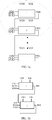
- FIG. 2a is a schematic diagram of a transmission control driver according to an embodiment of the present application.
- the emission control driver includes a plurality of cascaded emission control driving circuits.
- FIG. 2b is used for reference, that is an enlarged view of a repeating unit, shown in the dashed box of FIG. 2a .
- the repeating unit includes a first emission control driving circuit 1 and a second emission control driving circuit 2.
- the first emission control driving circuit 1 represents an odd emission control driving circuit
- the second emission control driving circuit 2 represents an even emission control driving circuit.
- the output terminal EMI of the first emission control driving circuit 1 is connected to the input terminal EIN of the second emission control driving circuit 2.
- the transmission control driver 400 in FIG. 2a is finally formed by repeating the connection according to the structure of the first transmission control driving circuit 1 and the second transmission control driving circuit 2.
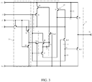
- FIG. 3 is a schematic diagram of a transmission control driving circuit according to an embodiment of the present application.
- the emission control driving circuit includes a first gate voltage control circuit 10, a second gate voltage control circuit 20, an output circuit 30 and an isolation circuit.
- the first gate voltage control circuit 10 generates a first gate-controlled voltage V1 according to signals of a first input terminal 11, a second input terminal 12 and a second power input terminal VGL.
- the second gate voltage control circuit 20 generates a second gate-controlled voltage V2 and a third gate-controlled voltage V3 according to the signals of the first gate-controlled voltage, the first input terminal 11, the second input terminal 12, a third input terminal 13, a first power input terminal VGH and the second power input terminal VGL.
- the output circuit 30 generates an output signal according to the signals of the second gate-controlled voltage V2, the third gate-controlled voltage V3, the first power input terminal VGH and the second power input terminal VGL.
- the isolation circuit is connected between the second power input terminal VGL and the first gate voltage control circuit 10, and between the second power input terminal VGL and the second gate voltage control circuit 20, ie, the isolation circuit is respectively connected to the second power input terminal VGL, the first gate voltage control circuit 10 and the second gate voltage control circuit 20.
- the isolation circuit respectively isolates the first gate-controlled voltage from the first gate voltage control circuit 10 and the second gate voltage control circuit 20, ie, a drain of a second transistor M2 is isolated from the first gate-controlled voltage, and a gate of the fifth transistor M5 is isolated from the first gate-controlled voltage.
- the isolation circuit isolates the third gate-controlled voltage from the second gate voltage control circuit 20, ie, a drain of the eighth transistor M8 is isolated from the third gate-controlled voltage.
- the first gate voltage control circuit 10 and the second gate voltage control circuit 20 each includes a plurality of transistors.
- One transistor of the first gate voltage control circuit 10 is connected to the first gate-controlled voltage
- two transistors of the second gate voltage control circuit 20 are respectively connected to the first gate-controlled voltage and the third gate-controlled voltage.
- the transistor connected between the first gate voltage control circuit 10 and the first gate-controlled voltage is the second transistor M2.
- the transistor connected between the second gate voltage control circuit 20 and the first gate-controlled voltage is a fifth transistor M5.
- the transistor connected between the second gate voltage control circuit 20 and the third gate-controlled voltage is an eighth transistor M8.
- the isolation circuit can prevent the first gate-controlled voltage V1 from being too low to cause damage to the transistor (the second transistor M2, the fifth transistor M5 or the eighth transistor M8), which is connected to the first gate-controlled voltage, in the first gate voltage control circuit or in the second gate voltage control circuit.
- the first gate voltage control circuit 10 includes a first transistor M1, the second transistor M2 and a third transistor M3.
- the first transistor M1, the second transistor M2 and the third transistor M3 may be P-type thin film transistors.
- the gate of the first transistor M1 is connected to the second input terminal 12, the source of the first transistor M1 is connected to the gate of the second transistor M2, and the drain of the first transistor M1 is connected to the first input terminal 11.
- the source of the second transistor M2 is connected to the second input terminal 12, the drain of the second transistor M2 is connected to the source of the third transistor M3, and the gate of the second transistor M2 is further connected to the second gate voltage control circuit 20.
- the gate of the third transistor M3 is connected to the second input terminal 12, the drain of the third transistor M3 is connected to the second power input terminal VGL, and the source of the third transistor M3 is further connected to the second gate voltage control circuit 20.
- the first gate voltage control circuit 10 includes more than one second transistors M2, and these second transistors M2 are sequentially connected. Specifically, the gates of these second transistors M2 are all connected to the source of the first transistors M1, and the source of each second transistor M2 is connected to the drain of the adjacent second transistor M2. Thus, by the series connection of these second transistors, the leakage current between the source and the drain can be reduced after the transistor is turned off, and the reliability of turning off the transistor can be improved.
- the second gate voltage control circuit 20 includes a fourth transistor M4, a fifth transistor M5, a sixth transistor M6, a seventh transistor M7, an eighth transistor M8 and a first capacitor C1.
- the fourth transistor M4, the fifth transistor M5, the sixth transistor M6, the seventh transistor M7 and the eighth transistor M8 may be P-type thin film transistors.
- the gate of the fourth transistor M4 is connected to the third input terminal 13, the source of the fourth transistor M4 is connected to the source of the fifth transistor M5, and the drain of the fourth transistor M4 is connected to the gate of the second transistor M2.
- the gate of the fifth transistor M5 (sequentially through the drain or the source of a twelfth transistor M12 and the drain or the source of a eleventh transistor M11) is coupled to the source of the third transistor M3, and the drain of the fifth transistor M5 is connected to the first power input terminal VGH.
- the gate of the sixth transistor M6 is connected to the source of the third transistor M3, the source of the sixth transistor M6 is connected to the source of the seventh transistor M7, and the drain of the sixth transistor M6 is connected to the third input terminal 13.
- the gate of the seventh transistor M7 is connected to the third input terminal 13, and the drain of the seventh transistor M7 is connected to the source of the eighth transistor M8.
- the gate of the eighth transistor M8 is connected to the first input terminal 11 and the output circuit 30.
- the drain of the eighth transistor M8 is connected to the first power input terminal VGH. And the source of the eighth transistor M8 is further connected to the output circuit 30.
- One end of the first capacitor C1 is connected to the gate of the sixth transistor M6, and the other end of the first capacitor C1 is connected to the source of the sixth transistor M6.
- the output circuit 30 includes a ninth transistor M9, a tenth transistor M10, a second capacitor C2 and a third capacitor C3.
- the ninth transistor M9 and the tenth transistor M10 may be P-type thin film transistors.
- the gate of the ninth transistor M9 is connected to the source of the eighth transistor M8.
- the source of the ninth transistor M9 is connected to the first power input terminal VGH.
- the drain of the ninth transistor M9 is connected to the source of the tenth transistor M10.
- the gate of the tenth transistor M10 is connected to the gate of the eighth transistor M8.
- the source of the tenth transistor M10 is connected to the output terminal 31.
- the drain of the tenth transistor M10 is connected to the second power input terminal VGL.
- One end of the second capacitor C2 is connected to the gate of the ninth transistor M9, and the other end of the second capacitor C2 is connected to the source of the ninth transistor M9.
- One end of the third capacitor C3 is connected to the gate of the tenth transistor M10, and the other end of the third capacitor C3 is connected to the third power input terminal 13.
- An output signal generated by the output circuit 30 is output from the output terminal 31.
- the isolation circuit includes an eleventh transistor M11, a twelfth transistor M12 and a thirteenth transistor M13.
- the eleventh transistor M11, the twelfth transistor M12 and the thirteenth transistor M13 may be P-type thin film transistors.
- the eleventh transistor M11 is connected between the source of the third transistor M3 and the gate of the sixth transistor M6.
- the gate of the eleventh transistor M11 is connected to the second power input terminal VGL.
- the source of the eleventh transistor M11 is connected to the source of the third transistor M3.
- the drain of the eleventh transistor M11 is connected to the gate of the sixth transistor M6.
- the twelfth transistor M12 is connected between the gate of the fifth transistor M5 and the gate of the sixth transistor M6.
- the gate of the twelfth transistor M12 is connected to the second power input terminal VGL.
- the drain of the twelfth transistor M12 is connected to the gate of the fifth transistor M5.
- the source of the twelfth transistor M12 is connected to the gate of the sixth transistor M6.
- the thirteenth transistor M13 is connected between the gate of the eighth transistor M8 and the gate of the tenth transistor M10.
- the gate of the thirteenth transistor M13 is connected to the second power input terminal VGL.
- the drain of the thirteenth transistor M13 is connected to the gate of the tenth transistor M10.
- the source of the thirteenth transistor M13 is connected to the gate of the eighth transistor M8.
- the gate of the sixth transistor M6 outputs the first gate-controlled voltage V1; the gate of the ninth transistor M9 outputs the second gate-controlled voltage V2; and the gate of the tenth transistor M10 outputs the third gate-controlled voltage V3.
- the first input terminal 11 receives an output signal of the previous emission control driving circuit.
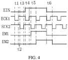
- the first input terminal 11 of the second emission control driving circuit 2 is connected to the output terminal 31 of the first emission control driving circuit 1, so as to receive the output signal EMI of the first emission control driving circuit 1, and a waveform of the output signal EMI is shown in FIG. 4 .
- the first input terminal 11 of the first emission control driving circuit 1 receives the start signal EIN, and a waveform of the start signal EIN is shown in FIG.4 .
- An odd emission control driving circuit for example, the second input terminal 12 of the first emission control driving circuit 1 receives a first clock signal ECK1, and the odd emission control driving circuit, for example, the third input terminal 13 of the first emission control driving circuit 1 receives a second clock signals ECK2.
- An even emission control driving circuit for example, the second input terminal 12 of the second emission control driving circuit 2 receives the second clock signal ECK2, and the even emission control driving circuit, for example, the third input terminal 13 of the second emission control driving circuit 2 receives the first clock signal ECK1.
- the waveforms of the first clock signal ECK1 and the second clock signal ECK2 are as shown in FIG.4 .
- transmission periods of the first clock signal ECK1 and the second clock signal ECK2 are the same, and the phases of the first clock signal and the second clock signal are non-overlapping.
- the start signal EIN changes to a rising edge voltage and maintains a high level voltage until the fourth falling edge voltage of the first clock signal ECK1 comes.
- the voltage of the first power input terminal VGH is higher than the voltage of the second power input terminal VGL.
- the embodiment of the present application also provides an emission control driver, including a plurality of the above-mentioned emission control drive circuits, the first input terminal of a latter emission control driver is connected to the output terminal of a former emission control driving circuit adjacent to the latter emission control driving circuit.
- the embodiment of the present application also provides an organic light emitting display device, including the emission control driver as described above.
- the isolation circuit respectively isolates the first gate-controlled voltage from the first gate voltage control circuit 10 and the second gate voltage control circuit 20, which can prevent the first gate-controlled voltage V1 from being too low to cause damage to the transistors (the second transistor M2 and the fifth transistor M5) in the first gate voltage control circuit or in the second gate voltage control circuit.
- the isolation circuit isolates the third gate-controlled voltage from the second gate voltage control circuit 20 (when the third gate-controlled voltage V3 is lower than the voltage of the second power input terminal VGL, the gate voltage of the thirteenth transistor M13 is greater than the source voltage of the thirteenth transistor M13, the thirteenth transistor M13 is turned off, so as to isolate the third gate-controlled voltage from the gate of the eighth transistor), which can prevent the third gate-controlled voltage V3 from being too low to cause damage to the transistor (the eighth transistor M8) in the second gate voltage control circuit 20.
- the isolation circuit includes the eleventh transistor M11, the twelfth transistor M12 and the thirteenth transistor M13.
- the eleventh transistor M11, the twelfth transistor M12 and the thirteenth transistor M13 are all P-type thin film transistors.
- the gates of the eleventh transistor M11, the twelfth transistor M12 and the thirteenth transistor M13 are connected to the second power input VGL.
- the eleventh transistor M11, the twelfth transistor M12 and the thirteenth transistor M13 are too low (below the voltage of the second power input terminal VGL), the eleventh transistor M11, the twelfth transistor M12 and the thirteenth transistor M13 are automatically turned off to isolate the source and drain.
- a timing waveform of the first emission control driving circuit is analyzed.
- the start signal EIN and the first clock signal ECK1 are at a low level in a first transmission period t1
- the second clock signal ECK2 is at a high level at the first transmission period t1.
- the eleventh transistor M11, the twelfth transistor M12 and the thirteenth transistor M13 are all P-type thin film transistors, and the gates of which are all connected to the second power input terminal. Therefore, in the normal case of the following analysis, the eleventh transistor M11, the twelfth transistor M12 and the thirteenth transistor M13 are equivalent to a conductive wire and will not be described herein.
- the first clock signal ECK1 with the low level is applied to the gate of the first transistor M1 and the gate of the third transistor M3. Therefore, the first transistor M1 and the third transistor M3 are turned on.
- the start signal EIN with the low level is applied to the gate of the second transistor M2 and the third gate-controlled voltage through the turned-on first transistor M1. Therefore, the second transistor M2 is turned on, and the third gate-controlled voltage V3 is at the low level.
- the first clock signal ECK1 with the low level and the second power input terminal VGL are applied the first gate-controlled voltage respectively through the turned-on second transistor M2 and the turned-on third transistor M3. Therefore, the first gate-controlled voltage V1 is set to the low level.
- the second clock signal ECK2 with the high level is applied to the fourth transistor M4 and the seventh transistor M7. Therefore, the fourth transistor M4 and the seventh transistor M7 are turned off.
- the eighth transistor M8 Since the third gate-controlled voltage V3 is at the low level, the eighth transistor M8 is turned on. The voltage of the first power input terminal VGH is applied to the second gate-controlled voltage through the turned-on eighth transistor M8. Therefore, the second gate-controlled voltage V2 is set to the high level. The second capacitor C2 is charged with the first power input terminal VGH. In other words, the second capacitor C2 is charged with a voltage having the high level. Since the second gate-controlled voltage V2 is at the high level, the ninth transistor M9 is turned off.
- the tenth transistor M10 Since the third gate-controlled voltage V3 is at the low level, the tenth transistor M10 is turned on. Due to the turned-on tenth transistor M10, the voltage of the second power input terminal VGL is applied to a first emission control line EMI, and therefore, the output signal EMI of the first emission control driving circuit is at the low level.
- the start signal EIN is at the low level
- the first clock signal ECK1 and the second clock signal ECK2 are at the high level.
- the first transistor M1 and the third transistor M3 are turned off through the first clock signal ECK1 with the high level.
- the second transistor M2 Since the third gate-controlled voltage V3 remains at the low level, the second transistor M2 is turned on. The first clock signal ECK1 with the high level is applied to the first gate-controlled voltage through the turned-on second transistor M2. Therefore, the first gate-controlled voltage V1 is at the high level.
- the third gate-controlled voltage V3 is at the low level, and therefore, the eighth transistor M8 and the tenth transistor M10 are turned on.
- the first power input terminal VGH is applied to the second gate-controlled voltage through the turned-on eighth transistor M8, so that the second gate-controlled voltage V2 is maintained at the high level.
- the ninth transistor M9 is turned off and the tenth transistor M10 is turned on. So that the first emission control signal EMI remains at the low level.
- the second clock signal ECK2 changes from the high level to the low level, and then changes from the low level to the high level again. Therefore, the third gate-controlled voltage V3 is bootstrapped by the change of an electric potential of the second clock signal ECK2, due to a coupling of the third capacitor C3.
- the third gate-controlled voltage V3 is still at the low level; when the second clock signal ECK2 at the third transmission period changes from the high level to the low level, the value of the third gate-controlled voltage V3 further reduced and be even lower than the voltage of the second power input terminal VGL because of the coupling of the third capacitor C3 (bootstrap effect).
- the gate voltage is much lower than the source voltage (the drain of the eighth transistor M8 is connected to the first power input terminal VGH, and at this time the eighth transistor M8 is turned on, a source voltage is also at the high level).
- the gate of the eighth transistor M8 is directly connected to the third gate-controlled voltage, breakdown damage may occur.
- the present embodiment adds the thirteenth transistor M13.
- the drain of the thirteenth transistor M13 is connected to the third gate-controlled voltage
- the gate of the thirteenth transistor M13 is connected to the second power input terminal VGL
- the third gate-controlled voltage V3 is lower than the second power input terminal VGL
- the thirteenth transistor M13 is quickly turned off, so that the eighth transistor M8 is isolated from the third gate-controlled voltage to prevent the eighth transistor M8 from being damaged.
- the source of the tenth transistor M10 (at this time the tenth transistor M10 is turned on) is connected to the second power input terminal VGL and is at the low level, so a voltage difference between the gate and the source of the tenth transistor M10 is small, the tenth transistor M10 will not be damaged and continues to be turned on, thereby the first emission control signal is kept at the low level.
- the start signal EIN and the second clock signal ECK2 are at the high level, and the first clock signal ECK1 is at the low level.
- the second clock signal ECK2 ends at the low level turns to the high level.
- the bootstrap effect is stopped by the voltage increase of the one end of the third capacitor C3 connected to the third input terminal 13; and the third capacitor C3 stops the coupling process.
- the third gate-controlled voltage V3 changes to the high level of the second power input terminal VGL from the low level, and the thirteenth transistor M13 maintains conduction.
- the first transistor M1 is turned on by the first clock signal ECK1 with the low level; and the start signal EIN with the high level is applied to the third gate-controlled voltage; and the third gate-controlled voltage V3 is at the high level. Therefore, the second transistor M2 and the tenth transistor M10 are turned off.
- the third transistor M3 is turned on in response to the first clock signal ECK1 with the low level and the second power input terminal VGL is applied to the first gate-controlled voltage V1. Therefore, the first gate-controlled voltage V1 is at the low level.
- the seventh transistor M7 is turned off in response to the second clock signal ECK2 with the high level. Since the third gate-controlled voltage V3 is at the high level, the eighth transistor M8 is turned off.
- the second gate-controlled voltage V2 is maintained at the high level by the charging effect of the second capacitor C2.
- the second gate-controlled voltage V2 is maintained at the high level, and therefore the ninth transistor M9 is turned off. Therefore, the first emission control signal is maintained at the low level.
- the start signal EIN and the first clock signal ECK1 are at the high level, and the second clock signal ECK2 is at the low level.
- the first transistor M1 and the third transistor M3 are turned off by the first clock signal ECK1 with the high level. Since the third gate-controlled voltage V3 is maintained at the high level, the second transistor M2, the eighth transistor M8 and the tenth transistor M10 are turned off.
- the fourth transistor M4 and the seventh transistor M7 are turned on in response to the second clock signal ECK2 having the low level.
- the first gate-controlled voltage V1 is set to the low level, so that the fifth transistor M5 and the sixth transistor M6 are turned on.
- the first gate-controlled voltage V1 is bootstrapped by the change of the electric potential of the second clock signal ECK2. Ie, when the second clock signal ECK2 is at the high level at the fourth time point t4, the first gate-controlled voltage V1 is still at the low level. When the second clock signal ECK2 changes from the high level to the low level at the fifth transmission point t5, the first gate-controlled voltage V1 is further reduced and even lower the voltage of the second power input terminal VGL because of the coupling (bootstrap effect) of the first capacitor C1.
- the present embodiment of the prevent application adds the eleventh transistor M11.
- the drain of the eleventh transistor M11 is connected to the first gate-controlled voltage
- the gate of the eleventh transistor M11 is connected to the second power input terminal VGL
- the eleventh transistor M11 is quickly turned off, so that the second transistor M2 is isolated from the first gate-controlled voltage to prevent the second transistor M2 from being damaged.
- the large decrease of the first gate-controlled voltage V1 also affects the fifth transistor M5.
- the gate of the fifth transistor M5 When the gate of the fifth transistor M5 is directly connected to the first gate-controlled voltage, and the drain of the fifth transistor M5 is connected to the first power input terminal VGH (a reference voltage of the present application is that the first power input terminal VGH is at the high level, about 7V; and since the fifth transistor M5 is turned on, the source of the fifth transistor M5 is also kept at about 7V, the gate the fifth transistor M5 is at about -17.2V, and the voltage between the gate and the source is 24.2V), then the gate source voltage being too large will cause breakdown damage. In order to avoid this risk, the present embodiment adds the twelfth transistor M12.
- the drain of the twelfth transistor M12 is connected to the first gate-controlled voltage
- the gate of the twelfth transistor M12 is connected to the second power input terminal VGL
- the first gate-controlled voltage V1 is lower than the voltage of the second power input terminal VGL
- the twelfth transistor M12 is quickly turned off, so that the fifth transistor M5 is isolated from the first gate-controlled voltage (after isolation, the gate voltage of the fifth transistor M5 is -5.3V, and the voltage between the gate and the source is reduced from 24.2V to 12.3V).
- the risk of a gate insulation breakdown by the high voltage is greatly reduced to prevent the fifth transistor M5 from being damaged.
- the second clock signal ECK2 with the low level is applied to the second gate-controlled voltage through the turned-on sixth transistor M6 and seventh transistor M7. Therefore, the second gate-controlled voltage V2 is at the low level at the fifth transmission point t5. Since the second gate-controlled voltage V2 is at the low level, the ninth transistor M9 is turned on.
- the ninth transistor M9 is turned on and the tenth transistor M10 is turned off, so that the first emission control signal is maintained at the high level.
- the start signal EIN and the first clock signal ECK1 are at the low level, and the second clock signal ECK2 is at the high level.
- the first emission control signal is set to the low level at the sixth transmission point t6.
- the first to ninth transistors M1-M9 are all P-type thin film transistors. In other embodiments, the first to ninth transistors M1-M9 may also be N-type thin film transistor.
- the P-type thin film transistors is turned on when the gate signal is at the low level, and the N-type thin film transistor is turned on when the gate signal is at the high level. Therefore, it is only necessary to match a selected transistor type with a turned-on electric potential.
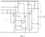
- the structures of the first gate voltage control circuit, the second gate voltage control circuit, and the output circuit are the same as described in the above-mentioned embodiment.
- the difference is that the isolation circuit is connected between the second power input terminal VGL and the first gate voltage control circuit 10 and the second gate voltage control circuit 20.
- the isolation circuit isolates the first gate-controlled voltage from the second gate voltage control circuit 20, ie, the gate of the fifth transistor M5 is isolated from the first gate-controlled voltage V1.
- the isolation circuit isolates the third gate-controlled voltage from the first gate voltage control circuit 10 and the second gate voltage control circuit 20, ie, the source of the second transistor M2 is isolated from the third gate-controlled voltage and the drain of the eighth transistor M8 is isolated from the third gate-controlled voltage.
- the isolation circuit includes a fourteenth transistor M14, a sixteenth transistor M16 and a fifteenth transistor M15.
- the fourteenth transistor M14, the sixteenth transistor M16 and the fifteenth transistor M15 are P-type thin film transistors.
- the fourteenth transistor M14 is connected between the gate of the second transistor M2 and the gate of the tenth transistor M10, the gate of the fourteenth transistor M14 is connected to the second power input terminal VGL, the source of the fourteenth transistor M14 is connect to the gate of the second transistor M2, and the drain of the fourteenth transistor M14 is connected to the gate of the tenth transistor M10.
- the structure and connection relationship of the sixteenth transistor M16 are the same as in the previous embodiment.
- the sixteenth transistor M16 is connected between the gate of the fifth transistor M5 and the gate of the sixth transistor M6, the gate of the sixteenth transistor M16 is connected to the second power input terminal VGL, the drain of the sixteenth transistor M16 is connected to the gate of the fifth transistor M5, and the source of the sixteenth transistor M16 is connected to the gate of the sixth transistor M6.
- the fifteenth transistor M15 is connected between the gate of the eighth transistor M8 and the gate of the tenth transistor M10, the gate of the fifteenth transistor M15 is connected to the second power input terminal VGL, the drain of the fifteenth transistor M15 is connected to the gate of the tenth transistor M10 and the drain of the fourteenth transistor M14, and the source of the fifteenth transistor M15 is connected to the gate of the eighth transistor M8.
- the isolation circuit includes the fourteenth transistor M14, the sixteenth transistor M16 and the fifteenth transistor M15, which are all P-type thin film transistors, and the gates of the fourteenth transistor M14, the sixteenth transistor M16 and the fifteenth transistor M15 are connected to the second power input VGL.
- the fourteenth transistor M14, the sixteenth transistor M16 and the fifteenth transistor M15 are automatically turned on.
- the fourteenth transistor M14, the sixteenth transistor M16 and the fifteenth transistor M15 are too low (below the second power input terminal VGL), the fourteenth transistor M14, the sixteenth transistor M16 and the fifteenth transistor M15 are automatically turned off to isolate the source and drain.
- a timing waveform of the first emission control driving circuit is analyzed.
- the start signal EIN and the first clock signal ECK1 are at a low level at the first transmission period t1
- the second clock signal ECK2 is at a high level in the first transmission period t1.
- the fourteenth transistor M14, the sixteenth transistor M16 and the fifteenth transistor M15 are all P-type thin film transistors, and the gates of those are connected to the second power input terminal VGL. Therefore, in the normal case of the following analysis, the fourteenth transistor M14, the sixteenth transistor M16 and the fifteenth transistor M15 are equivalent to a conductive wire and will not be described herein.
- the first clock signal ECK1 with the low level is applied to the gate of the first transistor M1 and the gate of the third transistor M3. Therefore, the first transistor M1 and the third transistor M3 are turned on.
- the start signal EIN with the low level is applied to the gate of the second transistor M2 and the third gate-controlled voltage through the turned-on first transistor M1. Therefore, the second transistor M2 is turned on, and the third gate-controlled voltage V3 is at the low level.
- the first clock signal ECK1 with the low level and the voltage of the second power input terminal VGL are applied to the first gate-controlled voltage respectively through the turned-on second transistor M2 and the turned-on third transistor M3. Therefore, the first gate-controlled voltage V1 is at the low level.
- the second clock signal ECK2 with the high level is applied to the fourth transistor M4 and the seventh transistor M7. Therefore, the fourth transistor M4 and the seventh transistor M7 are turned off.
- the eighth transistor M8 Since the third gate-controlled voltage V3 is at the low level, the eighth transistor M8 is turned on. The first power input terminal VGH is applied to the second gate-controlled voltage through the turned-on eighth transistor M8. Therefore, the second gate-controlled voltage V2 is at the high level. The second capacitor C2 is charged with the first power input terminal VGH. In other words, the second capacitor C2 is charged with a voltage having the high level. Since the second gate-controlled voltage V2 is at the high level, the ninth transistor M9 is turned off.
- the tenth transistor M10 Since the third gate-controlled voltage V3 is at the low level, the tenth transistor M10 is turned on. Due to the turned-on tenth transistor M10, a voltage of the second power input terminal VGL is applied to a first emission control line EM1, and therefore, the output signal EM1 of the first emission control driving circuit has the low level.
- the start signal EIN is at the low level
- the first clock signal ECK1 and the second clock signal ECK2 are at the high level.
- the first transistor M1 and the third transistor M3 are turned off through the first clock signal ECK1 with the high level.
- the third gate-controlled voltage V3 Since the third gate-controlled voltage V3 is maintained at the low level, the second transistor is turned on.
- the first clock signal ECK1 with the high level is applied to the first gate-controlled voltage. Therefore, the first gate-controlled voltage V1 is at the high level.
- the third gate-controlled voltage V3 is at the low level, and therefore, the eighth transistor M8 and the tenth transistor M10 are turned on.
- the voltage of the first power input terminal VGH is applied to the second gate-controlled voltage through the turned-on eighth transistor M8, so that the second gate-controlled voltage V2 is maintained at the high level.
- the ninth transistor M9 is turned off and the tenth transistor M10 is turned on. Therefore, the first emission control signal is maintained at the high level.
- the second clock signal ECK2 changes from the high level to the low level, and then changes from the low level to the high level again. Therefore, because of a coupling of the third capacitor C3, the third gate-controlled voltage V3 is bootstrapped by the change of an electric potential of the second clock signal ECK2. Ie, when the second clock signal ECK2 in the second transmission period is at the high level, the third gate-controlled voltage V3 is still at the low level; and when the second clock signal ECK2 in the third transmission period changes from the high level to the low level, the third gate-controlled voltage V3 further reduced and be even lower than the voltage of the second power input terminal VGL because of the coupling of the third capacitor C3 (bootstrap effect).
- the gate voltage is much lower than the source voltage (the drain of the second transistor M2 is connected to the second input terminal 12, and the first clock signal ECK1 is at the high level).
- the gate of the second transistor M2 is directly connected to the third gate-controlled voltage, breakdown damage may occur.
- the present embodiment adds the fourteenth transistor M14.
- the drain of the fourteenth transistor M14 is connected to the third gate-controlled voltage
- the gate of the fourteenth transistor M14 is connected to the second power input terminal VGL
- the fourteenth transistor M14 is quickly turned off, so that the second transistor M2 is isolated from the third gate-controlled voltage to prevent the second transistor M2 from being damaged.
- the gate voltage is much lower than the source voltage (the drain of the eighth transistor M8 is connected to the first power input terminal VGH, at this time the eighth transistor M8 is turned on, and a voltage of the source is also at the high level).
- the present embodiment adds the fifteenth transistor M15. At this time, the drain of the fifteenth transistor M15 is connected to the third gate-controlled voltage, the gate of the fifteenth transistor M15 is connected to the second power input terminal VGL, and since the third gate-controlled voltage V3 is lower than the voltage at the second power input terminal VGL, the fifteenth transistor M15 is quickly turned off, so that the eighth transistor M8 is isolated from the third gate voltage-controlled to prevent the eighth transistor M8 from being damaged.
- the source of the tenth transistor M10 (when the tenth transistor M10 is turned on) is connected to the second power input terminal VGL and is the low level, a voltage difference between the gate and the source of the tenth transistor M10 is small and the tenth transistor M10 will not be damaged and continues to be turned on, thereby the first emission control signal is kept at the low level.
- a fourth transmission period t4 the start signal EIN and the second clock signal ECK2 are at the high level, and the first clock signal ECK1 is at the low level.
- the second clock signal ECK2 ends at the low level and changes to the high level.
- the bootstrap effect is stopped by the voltage increase of the one end of the third capacitor C3 connected to the third input terminal 13; and the third capacitor C3 stops the coupling process.
- the third gate-controlled voltage V3 changes to the high level of the second power input terminal VGL from the low level, the fourteenth transistor M14 and the fifteenth transistor M15 maintain conduction.
- the first transistor M1 is turned on by the first clock signal ECK1 with the low level; and the start signal EIN with the high level is applied to the third gate-controlled voltage; and the third gate-controlled voltage V3 is at the high level. Therefore, the second transistor M2 and the tenth transistor M10 are turned off.
- the third transistor M3 is turned on in response to the first clock signal ECK1 with the low level, and the voltage of the second power input terminal VGL is applied to the first gate-controlled voltage V1. Therefore, the first gate-controlled voltage V1 is at the low level.
- the seventh transistor M7 is turned off in response to the second clock signal ECK2 having the high level. Since the third gate-controlled voltage V3 is at the high level, the eighth transistor M8 is turned off. The second gate-controlled voltage V2 is maintained at the high level by the charging effect of the second capacitor C2. The second gate-controlled voltage V2 is maintained at the high level, and therefore the ninth transistor M9 is turned off. Therefore, the first emission control signal is kept at the low level.
- the start signal EIN and the first clock signal ECK1 are at the high level, and the second clock signal ECK2 is at the low level.
- the first transistor M1 and the third transistor M3 are turned off by the first clock signal ECK1 with the high level. Since the third gate-controlled voltage V3 is maintained at the high level, the second transistor M2, the eighth transistor M8 and the tenth transistor M10 are turned off.
- the fourth transistor M4 and the seventh transistor M7 are turned on in response to the second clock signal ECK2 with the low level.
- the first gate-controlled voltage V1 is set the low level, so that the fifth transistor M5 and the sixth transistor M6 are turned on.
- the first gate-controlled voltage V1 is bootstrapped by the change of the electric potential of the second clock signal ECK2. I.e, when the second clock signal ECK2 is at the high level in the fourth transmission period t4, the first gate-controlled voltage V1 is still at the low level.
- the second clock signal ECK2 changes from the high level to the low level in the fifth transmission period t5, the first gate-controlled voltage V1 is further reduced and even lower the voltage of the second power input terminal VGL because of the coupling (bootstrap effect) of the first capacitor C1.
- the large decrease in the first gate-controlled voltage V1 also affects the fifth transistor M5.
- the present embodiment adds the sixteenth transistor M16.
- the source of the sixteenth transistor M16 is connected to the first gate-controlled voltage
- the gate of the sixteenth transistor M16 is connected to the second power input terminal VGL
- the sixteenth transistor M16 is quickly turned off, so that the fifth transistor M5 is isolated from the first gate-controlled voltage to prevent the fifth transistor M5 from being damaged.
- the second clock signal ECK2 with the low level is applied to the second gate-controlled voltage through the turned-on sixth transistor M6 and seventh transistor M7. Therefore, the second gate-controlled voltage V2 is at the low level in the fifth transmission period t5. Since the second gate-controlled voltage V2 is at the low level, the ninth transistor M9 is turned on.
- the ninth transistor M9 is turned on and the tenth transistor M10 is turned off, the first emission control signal is maintained at the high level.
- the start signal EIN and the first clock signal ECK1 are at the low level, and the second clock signal ECK2 is at the high level.
- the first emission control signal is at the low level in the sixth transmission period t6.
- the above-mentioned embodiments describe the different configurations of an emission control driving circuit in detail.
- the present application includes, but is not limited to, the configurations listed in the above embodiments. Any changes made to the configuration provided by the above-mentioned embodiments are within the scope of the present application. Those skilled in the art can make the same according to the content of the above-mentioned embodiments.
Landscapes
- Engineering & Computer Science (AREA)
- Physics & Mathematics (AREA)
- Computer Hardware Design (AREA)
- General Physics & Mathematics (AREA)
- Theoretical Computer Science (AREA)
- Control Of Indicators Other Than Cathode Ray Tubes (AREA)
- Electroluminescent Light Sources (AREA)
- Control Of El Displays (AREA)
Applications Claiming Priority (2)
| Application Number | Priority Date | Filing Date | Title |
|---|---|---|---|
| CN201810054293.XA CN108230998B (zh) | 2018-01-19 | 2018-01-19 | 发射控制驱动电路、发射控制驱动器及有机发光显示装置 |
| PCT/CN2018/107596 WO2019140947A1 (zh) | 2018-01-19 | 2018-09-26 | 发射控制驱动电路、发射控制驱动器及有机发光显示装置 |
Publications (3)
| Publication Number | Publication Date |
|---|---|
| EP3624103A1 true EP3624103A1 (de) | 2020-03-18 |
| EP3624103A4 EP3624103A4 (de) | 2020-05-13 |
| EP3624103B1 EP3624103B1 (de) | 2024-01-10 |
Family
ID=62668058
Family Applications (1)
| Application Number | Title | Priority Date | Filing Date |
|---|---|---|---|
| EP18901223.0A Active EP3624103B1 (de) | 2018-01-19 | 2018-09-26 | Treiberschaltung für emissionskontrolle, treiber für emissionskontrolle und organische lichtemittierende anzeigevorrichtung |
Country Status (7)
| Country | Link |
|---|---|
| US (1) | US10643533B2 (de) |
| EP (1) | EP3624103B1 (de) |
| JP (1) | JP6827131B2 (de) |
| KR (1) | KR102227391B1 (de) |
| CN (1) | CN108230998B (de) |
| TW (1) | TWI681379B (de) |
| WO (1) | WO2019140947A1 (de) |
Families Citing this family (4)
| Publication number | Priority date | Publication date | Assignee | Title |
|---|---|---|---|---|
| CN108230998B (zh) * | 2018-01-19 | 2020-01-24 | 昆山国显光电有限公司 | 发射控制驱动电路、发射控制驱动器及有机发光显示装置 |
| CN207781162U (zh) * | 2018-01-19 | 2018-08-28 | 昆山国显光电有限公司 | 一种发光控制电路、发光控制驱动器以及显示装置 |
| KR102718913B1 (ko) | 2019-03-18 | 2024-10-18 | 삼성디스플레이 주식회사 | 스테이지 및 이를 포함하는 발광 제어 구동부 |
| CN117012126B (zh) * | 2022-04-27 | 2024-09-24 | 荣耀终端有限公司 | 移位寄存器、栅极驱动电路、显示面板及电子设备 |
Family Cites Families (13)
| Publication number | Priority date | Publication date | Assignee | Title |
|---|---|---|---|---|
| KR100873072B1 (ko) * | 2006-08-31 | 2008-12-09 | 삼성모바일디스플레이주식회사 | 발광제어구동부 및 그를 이용한 유기전계발광표시장치 |
| KR101489968B1 (ko) * | 2008-04-18 | 2015-02-04 | 삼성디스플레이 주식회사 | 유기전계발광 표시장치 |
| KR101022173B1 (ko) * | 2009-01-13 | 2011-03-17 | 삼성모바일디스플레이주식회사 | 쉬프트 레지스터 및 이를 이용한 유기전계발광 표시장치 |
| KR101544052B1 (ko) * | 2009-02-11 | 2015-08-13 | 삼성디스플레이 주식회사 | 게이트 구동회로 및 이를 구비한 표시 장치 |
| TWI416530B (zh) * | 2009-03-25 | 2013-11-21 | Wintek Corp | 移位暫存器 |
| KR20120019691A (ko) * | 2010-08-26 | 2012-03-07 | 삼성모바일디스플레이주식회사 | 표시 장치 |
| KR101975581B1 (ko) * | 2012-08-21 | 2019-09-11 | 삼성디스플레이 주식회사 | 발광 제어 구동부 및 그것을 포함하는 유기발광 표시장치 |
| CN105185318B (zh) | 2015-10-19 | 2017-11-21 | 京东方科技集团股份有限公司 | 栅线驱动电路、输出发射控制信号的电路及触控显示装置 |
| CN106920498B (zh) * | 2015-12-25 | 2019-10-25 | 昆山工研院新型平板显示技术中心有限公司 | Gip电路及其驱动方法和平板显示装置 |
| KR102511947B1 (ko) * | 2016-06-17 | 2023-03-21 | 삼성디스플레이 주식회사 | 스테이지 및 이를 이용한 유기전계발광 표시장치 |
| CN206711576U (zh) * | 2017-01-22 | 2017-12-05 | 昆山国显光电有限公司 | 阵列基板行驱动单元的发射电路及阵列基板行驱动单元 |
| CN207068442U (zh) * | 2017-04-28 | 2018-03-02 | 昆山国显光电有限公司 | 发射控制驱动器及其显示装置 |
| CN108230998B (zh) * | 2018-01-19 | 2020-01-24 | 昆山国显光电有限公司 | 发射控制驱动电路、发射控制驱动器及有机发光显示装置 |
-
2018
- 2018-01-19 CN CN201810054293.XA patent/CN108230998B/zh active Active
- 2018-09-26 JP JP2019568738A patent/JP6827131B2/ja active Active
- 2018-09-26 WO PCT/CN2018/107596 patent/WO2019140947A1/zh not_active Ceased
- 2018-09-26 EP EP18901223.0A patent/EP3624103B1/de active Active
- 2018-09-26 KR KR1020197035996A patent/KR102227391B1/ko active Active
- 2018-10-09 TW TW107135521A patent/TWI681379B/zh active
-
2019
- 2019-03-05 US US16/293,486 patent/US10643533B2/en active Active
Also Published As
| Publication number | Publication date |
|---|---|
| TW201933324A (zh) | 2019-08-16 |
| EP3624103B1 (de) | 2024-01-10 |
| KR20190142409A (ko) | 2019-12-26 |
| TWI681379B (zh) | 2020-01-01 |
| CN108230998B (zh) | 2020-01-24 |
| WO2019140947A1 (zh) | 2019-07-25 |
| KR102227391B1 (ko) | 2021-03-12 |
| EP3624103A4 (de) | 2020-05-13 |
| CN108230998A (zh) | 2018-06-29 |
| US20190197956A1 (en) | 2019-06-27 |
| US10643533B2 (en) | 2020-05-05 |
| JP6827131B2 (ja) | 2021-02-10 |
| JP2020523641A (ja) | 2020-08-06 |
Similar Documents
| Publication | Publication Date | Title |
|---|---|---|
| US11210987B2 (en) | Shift register circuit, method of driving the same, gate driving circuit and display panel | |
| US11468922B2 (en) | Shift register, driving method thereof, gate driving circuit and display device | |
| US8963907B2 (en) | Pixel circuit and driving method thereof | |
| US10573245B2 (en) | Shift register unit using a bootstrap effect and driving method thereof, shift register and display device | |
| US9620241B2 (en) | Shift register unit, method for driving the same, shift register and display device | |
| US9898984B2 (en) | GOA circuit, display device and drive method of GOA circuit | |
| US20180301082A1 (en) | Level shifting unit, level shifting circuit, method for driving the level shifting circuit, gate driving circuit and display device | |
| US9324271B2 (en) | Pixel driver | |
| US10297203B2 (en) | Scanning driving circuit and flat display apparatus having the scanning driving circuit | |
| CN114078430A (zh) | 像素电路及显示面板 | |
| US10140930B2 (en) | Signal generating unit, shift register, display device and signal generating method | |
| US20190129560A1 (en) | Compensation circuit, gate driving unit, gate driving circuit, driving methods thereof and display device | |
| CN103268749A (zh) | 一种反相器、amoled补偿电路和显示面板 | |
| EP3624103A1 (de) | Treiberschaltung für emissionskontrolle, treiber für emissionskontrolle und organische lichtemittierende anzeigevorrichtung | |
| US11942035B2 (en) | Display panel, method for driving display panel, and display device | |
| CN104821146A (zh) | 栅极驱动电路及其单元和一种显示装置 | |
| US10134338B2 (en) | Inverter, gate driving circuit and display apparatus | |
| US20240169950A1 (en) | Goa circuit and display panel | |
| US12254838B2 (en) | Shift register unit, gate driver circuit, and display device | |
| US9805683B2 (en) | Gate driver on array circuit for different resolutions, driving method thereof, and display device including the same | |
| KR20200089328A (ko) | 액정 표시 패널 및 그 eoa 모듈 | |
| CN214226481U (zh) | 一种提高输出波形稳定性的gip电路 | |
| CN108711399B (zh) | 发射控制驱动电路、发射控制驱动器及有机发光显示装置 | |
| US20210065615A1 (en) | Shift Register Circuit and Method for Driving the Same, Gate Driving Circuit and Display Device | |
| CN112735320A (zh) | 一种提高输出波形稳定性的gip电路及驱动方法 |
Legal Events
| Date | Code | Title | Description |
|---|---|---|---|
| STAA | Information on the status of an ep patent application or granted ep patent |
Free format text: STATUS: THE INTERNATIONAL PUBLICATION HAS BEEN MADE |
|
| PUAI | Public reference made under article 153(3) epc to a published international application that has entered the european phase |
Free format text: ORIGINAL CODE: 0009012 |
|
| STAA | Information on the status of an ep patent application or granted ep patent |
Free format text: STATUS: REQUEST FOR EXAMINATION WAS MADE |
|
| 17P | Request for examination filed |
Effective date: 20191212 |
|
| AK | Designated contracting states |
Kind code of ref document: A1 Designated state(s): AL AT BE BG CH CY CZ DE DK EE ES FI FR GB GR HR HU IE IS IT LI LT LU LV MC MK MT NL NO PL PT RO RS SE SI SK SM TR |
|
| AX | Request for extension of the european patent |
Extension state: BA ME |
|
| A4 | Supplementary search report drawn up and despatched |
Effective date: 20200408 |
|
| RIC1 | Information provided on ipc code assigned before grant |
Ipc: G09G 3/3208 20160101AFI20200403BHEP |
|
| DAV | Request for validation of the european patent (deleted) | ||
| DAX | Request for extension of the european patent (deleted) | ||
| STAA | Information on the status of an ep patent application or granted ep patent |
Free format text: STATUS: EXAMINATION IS IN PROGRESS |
|
| 17Q | First examination report despatched |
Effective date: 20211022 |
|
| GRAP | Despatch of communication of intention to grant a patent |
Free format text: ORIGINAL CODE: EPIDOSNIGR1 |
|
| STAA | Information on the status of an ep patent application or granted ep patent |
Free format text: STATUS: GRANT OF PATENT IS INTENDED |
|
| INTG | Intention to grant announced |
Effective date: 20231025 |
|
| GRAS | Grant fee paid |
Free format text: ORIGINAL CODE: EPIDOSNIGR3 |
|
| GRAA | (expected) grant |
Free format text: ORIGINAL CODE: 0009210 |
|
| STAA | Information on the status of an ep patent application or granted ep patent |
Free format text: STATUS: THE PATENT HAS BEEN GRANTED |
|
| AK | Designated contracting states |
Kind code of ref document: B1 Designated state(s): AL AT BE BG CH CY CZ DE DK EE ES FI FR GB GR HR HU IE IS IT LI LT LU LV MC MK MT NL NO PL PT RO RS SE SI SK SM TR |
|
| REG | Reference to a national code |
Ref country code: GB Ref legal event code: FG4D |
|
| REG | Reference to a national code |
Ref country code: CH Ref legal event code: EP |
|
| REG | Reference to a national code |
Ref country code: DE Ref legal event code: R096 Ref document number: 602018064121 Country of ref document: DE |
|
| REG | Reference to a national code |
Ref country code: IE Ref legal event code: FG4D |
|
| REG | Reference to a national code |
Ref country code: LT Ref legal event code: MG9D |
|
| REG | Reference to a national code |
Ref country code: NL Ref legal event code: MP Effective date: 20240110 |
|
| REG | Reference to a national code |
Ref country code: AT Ref legal event code: MK05 Ref document number: 1649538 Country of ref document: AT Kind code of ref document: T Effective date: 20240110 |
|
| PG25 | Lapsed in a contracting state [announced via postgrant information from national office to epo] |
Ref country code: NL Free format text: LAPSE BECAUSE OF FAILURE TO SUBMIT A TRANSLATION OF THE DESCRIPTION OR TO PAY THE FEE WITHIN THE PRESCRIBED TIME-LIMIT Effective date: 20240110 |
|
| PG25 | Lapsed in a contracting state [announced via postgrant information from national office to epo] |
Ref country code: NL Free format text: LAPSE BECAUSE OF FAILURE TO SUBMIT A TRANSLATION OF THE DESCRIPTION OR TO PAY THE FEE WITHIN THE PRESCRIBED TIME-LIMIT Effective date: 20240110 |
|
| PG25 | Lapsed in a contracting state [announced via postgrant information from national office to epo] |
Ref country code: IS Free format text: LAPSE BECAUSE OF FAILURE TO SUBMIT A TRANSLATION OF THE DESCRIPTION OR TO PAY THE FEE WITHIN THE PRESCRIBED TIME-LIMIT Effective date: 20240510 |
|
| PG25 | Lapsed in a contracting state [announced via postgrant information from national office to epo] |
Ref country code: LT Free format text: LAPSE BECAUSE OF FAILURE TO SUBMIT A TRANSLATION OF THE DESCRIPTION OR TO PAY THE FEE WITHIN THE PRESCRIBED TIME-LIMIT Effective date: 20240110 |
|
| PG25 | Lapsed in a contracting state [announced via postgrant information from national office to epo] |
Ref country code: GR Free format text: LAPSE BECAUSE OF FAILURE TO SUBMIT A TRANSLATION OF THE DESCRIPTION OR TO PAY THE FEE WITHIN THE PRESCRIBED TIME-LIMIT Effective date: 20240411 |
|
| PG25 | Lapsed in a contracting state [announced via postgrant information from national office to epo] |
Ref country code: HR Free format text: LAPSE BECAUSE OF FAILURE TO SUBMIT A TRANSLATION OF THE DESCRIPTION OR TO PAY THE FEE WITHIN THE PRESCRIBED TIME-LIMIT Effective date: 20240110 Ref country code: RS Free format text: LAPSE BECAUSE OF FAILURE TO SUBMIT A TRANSLATION OF THE DESCRIPTION OR TO PAY THE FEE WITHIN THE PRESCRIBED TIME-LIMIT Effective date: 20240410 |
|
| PG25 | Lapsed in a contracting state [announced via postgrant information from national office to epo] |
Ref country code: ES Free format text: LAPSE BECAUSE OF FAILURE TO SUBMIT A TRANSLATION OF THE DESCRIPTION OR TO PAY THE FEE WITHIN THE PRESCRIBED TIME-LIMIT Effective date: 20240110 |
|
| PG25 | Lapsed in a contracting state [announced via postgrant information from national office to epo] |
Ref country code: AT Free format text: LAPSE BECAUSE OF FAILURE TO SUBMIT A TRANSLATION OF THE DESCRIPTION OR TO PAY THE FEE WITHIN THE PRESCRIBED TIME-LIMIT Effective date: 20240110 |
|
| PG25 | Lapsed in a contracting state [announced via postgrant information from national office to epo] |
Ref country code: RS Free format text: LAPSE BECAUSE OF FAILURE TO SUBMIT A TRANSLATION OF THE DESCRIPTION OR TO PAY THE FEE WITHIN THE PRESCRIBED TIME-LIMIT Effective date: 20240410 Ref country code: NO Free format text: LAPSE BECAUSE OF FAILURE TO SUBMIT A TRANSLATION OF THE DESCRIPTION OR TO PAY THE FEE WITHIN THE PRESCRIBED TIME-LIMIT Effective date: 20240410 Ref country code: LT Free format text: LAPSE BECAUSE OF FAILURE TO SUBMIT A TRANSLATION OF THE DESCRIPTION OR TO PAY THE FEE WITHIN THE PRESCRIBED TIME-LIMIT Effective date: 20240110 Ref country code: IS Free format text: LAPSE BECAUSE OF FAILURE TO SUBMIT A TRANSLATION OF THE DESCRIPTION OR TO PAY THE FEE WITHIN THE PRESCRIBED TIME-LIMIT Effective date: 20240510 Ref country code: HR Free format text: LAPSE BECAUSE OF FAILURE TO SUBMIT A TRANSLATION OF THE DESCRIPTION OR TO PAY THE FEE WITHIN THE PRESCRIBED TIME-LIMIT Effective date: 20240110 Ref country code: GR Free format text: LAPSE BECAUSE OF FAILURE TO SUBMIT A TRANSLATION OF THE DESCRIPTION OR TO PAY THE FEE WITHIN THE PRESCRIBED TIME-LIMIT Effective date: 20240411 Ref country code: ES Free format text: LAPSE BECAUSE OF FAILURE TO SUBMIT A TRANSLATION OF THE DESCRIPTION OR TO PAY THE FEE WITHIN THE PRESCRIBED TIME-LIMIT Effective date: 20240110 Ref country code: BG Free format text: LAPSE BECAUSE OF FAILURE TO SUBMIT A TRANSLATION OF THE DESCRIPTION OR TO PAY THE FEE WITHIN THE PRESCRIBED TIME-LIMIT Effective date: 20240110 Ref country code: AT Free format text: LAPSE BECAUSE OF FAILURE TO SUBMIT A TRANSLATION OF THE DESCRIPTION OR TO PAY THE FEE WITHIN THE PRESCRIBED TIME-LIMIT Effective date: 20240110 |
|
| PG25 | Lapsed in a contracting state [announced via postgrant information from national office to epo] |
Ref country code: PL Free format text: LAPSE BECAUSE OF FAILURE TO SUBMIT A TRANSLATION OF THE DESCRIPTION OR TO PAY THE FEE WITHIN THE PRESCRIBED TIME-LIMIT Effective date: 20240110 Ref country code: PT Free format text: LAPSE BECAUSE OF FAILURE TO SUBMIT A TRANSLATION OF THE DESCRIPTION OR TO PAY THE FEE WITHIN THE PRESCRIBED TIME-LIMIT Effective date: 20240510 |
|
| PG25 | Lapsed in a contracting state [announced via postgrant information from national office to epo] |
Ref country code: SE Free format text: LAPSE BECAUSE OF FAILURE TO SUBMIT A TRANSLATION OF THE DESCRIPTION OR TO PAY THE FEE WITHIN THE PRESCRIBED TIME-LIMIT Effective date: 20240110 Ref country code: PT Free format text: LAPSE BECAUSE OF FAILURE TO SUBMIT A TRANSLATION OF THE DESCRIPTION OR TO PAY THE FEE WITHIN THE PRESCRIBED TIME-LIMIT Effective date: 20240510 Ref country code: PL Free format text: LAPSE BECAUSE OF FAILURE TO SUBMIT A TRANSLATION OF THE DESCRIPTION OR TO PAY THE FEE WITHIN THE PRESCRIBED TIME-LIMIT Effective date: 20240110 Ref country code: LV Free format text: LAPSE BECAUSE OF FAILURE TO SUBMIT A TRANSLATION OF THE DESCRIPTION OR TO PAY THE FEE WITHIN THE PRESCRIBED TIME-LIMIT Effective date: 20240110 |
|
| PG25 | Lapsed in a contracting state [announced via postgrant information from national office to epo] |
Ref country code: DK Free format text: LAPSE BECAUSE OF FAILURE TO SUBMIT A TRANSLATION OF THE DESCRIPTION OR TO PAY THE FEE WITHIN THE PRESCRIBED TIME-LIMIT Effective date: 20240110 |
|
| REG | Reference to a national code |
Ref country code: DE Ref legal event code: R097 Ref document number: 602018064121 Country of ref document: DE |
|
| PG25 | Lapsed in a contracting state [announced via postgrant information from national office to epo] |
Ref country code: SM Free format text: LAPSE BECAUSE OF FAILURE TO SUBMIT A TRANSLATION OF THE DESCRIPTION OR TO PAY THE FEE WITHIN THE PRESCRIBED TIME-LIMIT Effective date: 20240110 |
|
| PG25 | Lapsed in a contracting state [announced via postgrant information from national office to epo] |
Ref country code: CZ Free format text: LAPSE BECAUSE OF FAILURE TO SUBMIT A TRANSLATION OF THE DESCRIPTION OR TO PAY THE FEE WITHIN THE PRESCRIBED TIME-LIMIT Effective date: 20240110 Ref country code: EE Free format text: LAPSE BECAUSE OF FAILURE TO SUBMIT A TRANSLATION OF THE DESCRIPTION OR TO PAY THE FEE WITHIN THE PRESCRIBED TIME-LIMIT Effective date: 20240110 |
|
| PG25 | Lapsed in a contracting state [announced via postgrant information from national office to epo] |
Ref country code: SK Free format text: LAPSE BECAUSE OF FAILURE TO SUBMIT A TRANSLATION OF THE DESCRIPTION OR TO PAY THE FEE WITHIN THE PRESCRIBED TIME-LIMIT Effective date: 20240110 |
|
| PG25 | Lapsed in a contracting state [announced via postgrant information from national office to epo] |
Ref country code: SM Free format text: LAPSE BECAUSE OF FAILURE TO SUBMIT A TRANSLATION OF THE DESCRIPTION OR TO PAY THE FEE WITHIN THE PRESCRIBED TIME-LIMIT Effective date: 20240110 Ref country code: SK Free format text: LAPSE BECAUSE OF FAILURE TO SUBMIT A TRANSLATION OF THE DESCRIPTION OR TO PAY THE FEE WITHIN THE PRESCRIBED TIME-LIMIT Effective date: 20240110 Ref country code: RO Free format text: LAPSE BECAUSE OF FAILURE TO SUBMIT A TRANSLATION OF THE DESCRIPTION OR TO PAY THE FEE WITHIN THE PRESCRIBED TIME-LIMIT Effective date: 20240110 Ref country code: EE Free format text: LAPSE BECAUSE OF FAILURE TO SUBMIT A TRANSLATION OF THE DESCRIPTION OR TO PAY THE FEE WITHIN THE PRESCRIBED TIME-LIMIT Effective date: 20240110 Ref country code: DK Free format text: LAPSE BECAUSE OF FAILURE TO SUBMIT A TRANSLATION OF THE DESCRIPTION OR TO PAY THE FEE WITHIN THE PRESCRIBED TIME-LIMIT Effective date: 20240110 Ref country code: CZ Free format text: LAPSE BECAUSE OF FAILURE TO SUBMIT A TRANSLATION OF THE DESCRIPTION OR TO PAY THE FEE WITHIN THE PRESCRIBED TIME-LIMIT Effective date: 20240110 |
|
| PLBE | No opposition filed within time limit |
Free format text: ORIGINAL CODE: 0009261 |
|
| STAA | Information on the status of an ep patent application or granted ep patent |
Free format text: STATUS: NO OPPOSITION FILED WITHIN TIME LIMIT |
|
| PG25 | Lapsed in a contracting state [announced via postgrant information from national office to epo] |
Ref country code: IT Free format text: LAPSE BECAUSE OF FAILURE TO SUBMIT A TRANSLATION OF THE DESCRIPTION OR TO PAY THE FEE WITHIN THE PRESCRIBED TIME-LIMIT Effective date: 20240110 |
|
| 26N | No opposition filed |
Effective date: 20241011 |
|
| PG25 | Lapsed in a contracting state [announced via postgrant information from national office to epo] |
Ref country code: IT Free format text: LAPSE BECAUSE OF FAILURE TO SUBMIT A TRANSLATION OF THE DESCRIPTION OR TO PAY THE FEE WITHIN THE PRESCRIBED TIME-LIMIT Effective date: 20240110 |
|
| PG25 | Lapsed in a contracting state [announced via postgrant information from national office to epo] |
Ref country code: SI Free format text: LAPSE BECAUSE OF FAILURE TO SUBMIT A TRANSLATION OF THE DESCRIPTION OR TO PAY THE FEE WITHIN THE PRESCRIBED TIME-LIMIT Effective date: 20240110 Ref country code: MC Free format text: LAPSE BECAUSE OF FAILURE TO SUBMIT A TRANSLATION OF THE DESCRIPTION OR TO PAY THE FEE WITHIN THE PRESCRIBED TIME-LIMIT Effective date: 20240110 |
|
| REG | Reference to a national code |
Ref country code: CH Ref legal event code: PL |
|
| PG25 | Lapsed in a contracting state [announced via postgrant information from national office to epo] |
Ref country code: LU Free format text: LAPSE BECAUSE OF NON-PAYMENT OF DUE FEES Effective date: 20240926 |
|
| REG | Reference to a national code |
Ref country code: BE Ref legal event code: MM Effective date: 20240930 |
|
| PG25 | Lapsed in a contracting state [announced via postgrant information from national office to epo] |
Ref country code: BE Free format text: LAPSE BECAUSE OF NON-PAYMENT OF DUE FEES Effective date: 20240930 |
|
| PG25 | Lapsed in a contracting state [announced via postgrant information from national office to epo] |
Ref country code: CH Free format text: LAPSE BECAUSE OF NON-PAYMENT OF DUE FEES Effective date: 20240930 |
|
| PG25 | Lapsed in a contracting state [announced via postgrant information from national office to epo] |
Ref country code: IE Free format text: LAPSE BECAUSE OF NON-PAYMENT OF DUE FEES Effective date: 20240926 |
|
| PG25 | Lapsed in a contracting state [announced via postgrant information from national office to epo] |
Ref country code: FI Free format text: LAPSE BECAUSE OF FAILURE TO SUBMIT A TRANSLATION OF THE DESCRIPTION OR TO PAY THE FEE WITHIN THE PRESCRIBED TIME-LIMIT Effective date: 20240110 |
|
| PGFP | Annual fee paid to national office [announced via postgrant information from national office to epo] |
Ref country code: DE Payment date: 20250916 Year of fee payment: 8 |
|
| PGFP | Annual fee paid to national office [announced via postgrant information from national office to epo] |
Ref country code: GB Payment date: 20250919 Year of fee payment: 8 |
|
| PGFP | Annual fee paid to national office [announced via postgrant information from national office to epo] |
Ref country code: FR Payment date: 20250929 Year of fee payment: 8 |
|
| PG25 | Lapsed in a contracting state [announced via postgrant information from national office to epo] |
Ref country code: CY Free format text: LAPSE BECAUSE OF FAILURE TO SUBMIT A TRANSLATION OF THE DESCRIPTION OR TO PAY THE FEE WITHIN THE PRESCRIBED TIME-LIMIT; INVALID AB INITIO Effective date: 20180926 |
|
| PG25 | Lapsed in a contracting state [announced via postgrant information from national office to epo] |
Ref country code: HU Free format text: LAPSE BECAUSE OF FAILURE TO SUBMIT A TRANSLATION OF THE DESCRIPTION OR TO PAY THE FEE WITHIN THE PRESCRIBED TIME-LIMIT; INVALID AB INITIO Effective date: 20180926 |