EP3624178A1 - Procédé de découpe de grille, de contact et d'ailette - Google Patents
Procédé de découpe de grille, de contact et d'ailette Download PDFInfo
- Publication number
- EP3624178A1 EP3624178A1 EP18193824.2A EP18193824A EP3624178A1 EP 3624178 A1 EP3624178 A1 EP 3624178A1 EP 18193824 A EP18193824 A EP 18193824A EP 3624178 A1 EP3624178 A1 EP 3624178A1
- Authority
- EP
- European Patent Office
- Prior art keywords
- contact
- gate
- fins
- metal
- present
- Prior art date
- Legal status (The legal status is an assumption and is not a legal conclusion. Google has not performed a legal analysis and makes no representation as to the accuracy of the status listed.)
- Withdrawn
Links
Images




Classifications
-
- H—ELECTRICITY
- H10—SEMICONDUCTOR DEVICES; ELECTRIC SOLID-STATE DEVICES NOT OTHERWISE PROVIDED FOR
- H10P—GENERIC PROCESSES OR APPARATUS FOR THE MANUFACTURE OR TREATMENT OF DEVICES COVERED BY CLASS H10
- H10P52/00—Grinding, lapping or polishing of wafers, substrates or parts of devices
-
- H—ELECTRICITY
- H10—SEMICONDUCTOR DEVICES; ELECTRIC SOLID-STATE DEVICES NOT OTHERWISE PROVIDED FOR
- H10D—INORGANIC ELECTRIC SEMICONDUCTOR DEVICES
- H10D84/00—Integrated devices formed in or on semiconductor substrates that comprise only semiconducting layers, e.g. on Si wafers or on GaAs-on-Si wafers
- H10D84/01—Manufacture or treatment
- H10D84/0123—Integrating together multiple components covered by H10D12/00 or H10D30/00, e.g. integrating multiple IGBTs
- H10D84/0126—Integrating together multiple components covered by H10D12/00 or H10D30/00, e.g. integrating multiple IGBTs the components including insulated gates, e.g. IGFETs
- H10D84/0151—Manufacturing their isolation regions
-
- H—ELECTRICITY
- H10—SEMICONDUCTOR DEVICES; ELECTRIC SOLID-STATE DEVICES NOT OTHERWISE PROVIDED FOR
- H10B—ELECTRONIC MEMORY DEVICES
- H10B10/00—Static random access memory [SRAM] devices
- H10B10/12—Static random access memory [SRAM] devices comprising a MOSFET load element
-
- H—ELECTRICITY
- H10—SEMICONDUCTOR DEVICES; ELECTRIC SOLID-STATE DEVICES NOT OTHERWISE PROVIDED FOR
- H10D—INORGANIC ELECTRIC SEMICONDUCTOR DEVICES
- H10D30/00—Field-effect transistors [FET]
- H10D30/60—Insulated-gate field-effect transistors [IGFET]
- H10D30/62—Fin field-effect transistors [FinFET]
- H10D30/6219—Fin field-effect transistors [FinFET] characterised by the source or drain electrodes
-
- H—ELECTRICITY
- H10—SEMICONDUCTOR DEVICES; ELECTRIC SOLID-STATE DEVICES NOT OTHERWISE PROVIDED FOR
- H10D—INORGANIC ELECTRIC SEMICONDUCTOR DEVICES
- H10D30/00—Field-effect transistors [FET]
- H10D30/60—Insulated-gate field-effect transistors [IGFET]
- H10D30/751—Insulated-gate field-effect transistors [IGFET] having composition variations in the channel regions
-
- H—ELECTRICITY
- H10—SEMICONDUCTOR DEVICES; ELECTRIC SOLID-STATE DEVICES NOT OTHERWISE PROVIDED FOR
- H10D—INORGANIC ELECTRIC SEMICONDUCTOR DEVICES
- H10D30/00—Field-effect transistors [FET]
- H10D30/60—Insulated-gate field-effect transistors [IGFET]
- H10D30/791—Arrangements for exerting mechanical stress on the crystal lattice of the channel regions
- H10D30/797—Arrangements for exerting mechanical stress on the crystal lattice of the channel regions being in source or drain regions, e.g. SiGe source or drain
-
- H—ELECTRICITY
- H10—SEMICONDUCTOR DEVICES; ELECTRIC SOLID-STATE DEVICES NOT OTHERWISE PROVIDED FOR
- H10D—INORGANIC ELECTRIC SEMICONDUCTOR DEVICES
- H10D30/00—Field-effect transistors [FET]
- H10D30/60—Insulated-gate field-effect transistors [IGFET]
- H10D30/791—Arrangements for exerting mechanical stress on the crystal lattice of the channel regions
- H10D30/798—Arrangements for exerting mechanical stress on the crystal lattice of the channel regions being provided in or under the channel regions
-
- H—ELECTRICITY
- H10—SEMICONDUCTOR DEVICES; ELECTRIC SOLID-STATE DEVICES NOT OTHERWISE PROVIDED FOR
- H10D—INORGANIC ELECTRIC SEMICONDUCTOR DEVICES
- H10D62/00—Semiconductor bodies, or regions thereof, of devices having potential barriers
- H10D62/80—Semiconductor bodies, or regions thereof, of devices having potential barriers characterised by the materials
- H10D62/83—Semiconductor bodies, or regions thereof, of devices having potential barriers characterised by the materials being Group IV materials, e.g. B-doped Si or undoped Ge
-
- H—ELECTRICITY
- H10—SEMICONDUCTOR DEVICES; ELECTRIC SOLID-STATE DEVICES NOT OTHERWISE PROVIDED FOR
- H10D—INORGANIC ELECTRIC SEMICONDUCTOR DEVICES
- H10D62/00—Semiconductor bodies, or regions thereof, of devices having potential barriers
- H10D62/80—Semiconductor bodies, or regions thereof, of devices having potential barriers characterised by the materials
- H10D62/83—Semiconductor bodies, or regions thereof, of devices having potential barriers characterised by the materials being Group IV materials, e.g. B-doped Si or undoped Ge
- H10D62/832—Semiconductor bodies, or regions thereof, of devices having potential barriers characterised by the materials being Group IV materials, e.g. B-doped Si or undoped Ge being Group IV materials comprising two or more elements, e.g. SiGe
-
- H—ELECTRICITY
- H10—SEMICONDUCTOR DEVICES; ELECTRIC SOLID-STATE DEVICES NOT OTHERWISE PROVIDED FOR
- H10D—INORGANIC ELECTRIC SEMICONDUCTOR DEVICES
- H10D62/00—Semiconductor bodies, or regions thereof, of devices having potential barriers
- H10D62/80—Semiconductor bodies, or regions thereof, of devices having potential barriers characterised by the materials
- H10D62/85—Semiconductor bodies, or regions thereof, of devices having potential barriers characterised by the materials being Group III-V materials, e.g. GaAs
-
- H—ELECTRICITY
- H10—SEMICONDUCTOR DEVICES; ELECTRIC SOLID-STATE DEVICES NOT OTHERWISE PROVIDED FOR
- H10D—INORGANIC ELECTRIC SEMICONDUCTOR DEVICES
- H10D64/00—Electrodes of devices having potential barriers
- H10D64/01—Manufacture or treatment
- H10D64/017—Manufacture or treatment using dummy gates in processes wherein at least parts of the final gates are self-aligned to the dummy gates, i.e. replacement gate processes
-
- H—ELECTRICITY
- H10—SEMICONDUCTOR DEVICES; ELECTRIC SOLID-STATE DEVICES NOT OTHERWISE PROVIDED FOR
- H10D—INORGANIC ELECTRIC SEMICONDUCTOR DEVICES
- H10D84/00—Integrated devices formed in or on semiconductor substrates that comprise only semiconducting layers, e.g. on Si wafers or on GaAs-on-Si wafers
- H10D84/01—Manufacture or treatment
- H10D84/0123—Integrating together multiple components covered by H10D12/00 or H10D30/00, e.g. integrating multiple IGBTs
- H10D84/0126—Integrating together multiple components covered by H10D12/00 or H10D30/00, e.g. integrating multiple IGBTs the components including insulated gates, e.g. IGFETs
- H10D84/0158—Integrating together multiple components covered by H10D12/00 or H10D30/00, e.g. integrating multiple IGBTs the components including insulated gates, e.g. IGFETs the components including FinFETs
-
- H—ELECTRICITY
- H10—SEMICONDUCTOR DEVICES; ELECTRIC SOLID-STATE DEVICES NOT OTHERWISE PROVIDED FOR
- H10D—INORGANIC ELECTRIC SEMICONDUCTOR DEVICES
- H10D84/00—Integrated devices formed in or on semiconductor substrates that comprise only semiconducting layers, e.g. on Si wafers or on GaAs-on-Si wafers
- H10D84/01—Manufacture or treatment
- H10D84/0123—Integrating together multiple components covered by H10D12/00 or H10D30/00, e.g. integrating multiple IGBTs
- H10D84/0126—Integrating together multiple components covered by H10D12/00 or H10D30/00, e.g. integrating multiple IGBTs the components including insulated gates, e.g. IGFETs
- H10D84/0165—Integrating together multiple components covered by H10D12/00 or H10D30/00, e.g. integrating multiple IGBTs the components including insulated gates, e.g. IGFETs the components including complementary IGFETs, e.g. CMOS devices
- H10D84/0167—Manufacturing their channels
-
- H—ELECTRICITY
- H10—SEMICONDUCTOR DEVICES; ELECTRIC SOLID-STATE DEVICES NOT OTHERWISE PROVIDED FOR
- H10D—INORGANIC ELECTRIC SEMICONDUCTOR DEVICES
- H10D84/00—Integrated devices formed in or on semiconductor substrates that comprise only semiconducting layers, e.g. on Si wafers or on GaAs-on-Si wafers
- H10D84/01—Manufacture or treatment
- H10D84/0123—Integrating together multiple components covered by H10D12/00 or H10D30/00, e.g. integrating multiple IGBTs
- H10D84/0126—Integrating together multiple components covered by H10D12/00 or H10D30/00, e.g. integrating multiple IGBTs the components including insulated gates, e.g. IGFETs
- H10D84/0165—Integrating together multiple components covered by H10D12/00 or H10D30/00, e.g. integrating multiple IGBTs the components including insulated gates, e.g. IGFETs the components including complementary IGFETs, e.g. CMOS devices
- H10D84/017—Manufacturing their source or drain regions, e.g. silicided source or drain regions
-
- H—ELECTRICITY
- H10—SEMICONDUCTOR DEVICES; ELECTRIC SOLID-STATE DEVICES NOT OTHERWISE PROVIDED FOR
- H10D—INORGANIC ELECTRIC SEMICONDUCTOR DEVICES
- H10D84/00—Integrated devices formed in or on semiconductor substrates that comprise only semiconducting layers, e.g. on Si wafers or on GaAs-on-Si wafers
- H10D84/01—Manufacture or treatment
- H10D84/0123—Integrating together multiple components covered by H10D12/00 or H10D30/00, e.g. integrating multiple IGBTs
- H10D84/0126—Integrating together multiple components covered by H10D12/00 or H10D30/00, e.g. integrating multiple IGBTs the components including insulated gates, e.g. IGFETs
- H10D84/0165—Integrating together multiple components covered by H10D12/00 or H10D30/00, e.g. integrating multiple IGBTs the components including insulated gates, e.g. IGFETs the components including complementary IGFETs, e.g. CMOS devices
- H10D84/0172—Manufacturing their gate conductors
-
- H—ELECTRICITY
- H10—SEMICONDUCTOR DEVICES; ELECTRIC SOLID-STATE DEVICES NOT OTHERWISE PROVIDED FOR
- H10D—INORGANIC ELECTRIC SEMICONDUCTOR DEVICES
- H10D84/00—Integrated devices formed in or on semiconductor substrates that comprise only semiconducting layers, e.g. on Si wafers or on GaAs-on-Si wafers
- H10D84/01—Manufacture or treatment
- H10D84/0123—Integrating together multiple components covered by H10D12/00 or H10D30/00, e.g. integrating multiple IGBTs
- H10D84/0126—Integrating together multiple components covered by H10D12/00 or H10D30/00, e.g. integrating multiple IGBTs the components including insulated gates, e.g. IGFETs
- H10D84/0165—Integrating together multiple components covered by H10D12/00 or H10D30/00, e.g. integrating multiple IGBTs the components including insulated gates, e.g. IGFETs the components including complementary IGFETs, e.g. CMOS devices
- H10D84/0186—Manufacturing their interconnections or electrodes, e.g. source or drain electrodes
-
- H—ELECTRICITY
- H10—SEMICONDUCTOR DEVICES; ELECTRIC SOLID-STATE DEVICES NOT OTHERWISE PROVIDED FOR
- H10D—INORGANIC ELECTRIC SEMICONDUCTOR DEVICES
- H10D84/00—Integrated devices formed in or on semiconductor substrates that comprise only semiconducting layers, e.g. on Si wafers or on GaAs-on-Si wafers
- H10D84/01—Manufacture or treatment
- H10D84/0123—Integrating together multiple components covered by H10D12/00 or H10D30/00, e.g. integrating multiple IGBTs
- H10D84/0126—Integrating together multiple components covered by H10D12/00 or H10D30/00, e.g. integrating multiple IGBTs the components including insulated gates, e.g. IGFETs
- H10D84/0165—Integrating together multiple components covered by H10D12/00 or H10D30/00, e.g. integrating multiple IGBTs the components including insulated gates, e.g. IGFETs the components including complementary IGFETs, e.g. CMOS devices
- H10D84/0193—Integrating together multiple components covered by H10D12/00 or H10D30/00, e.g. integrating multiple IGBTs the components including insulated gates, e.g. IGFETs the components including complementary IGFETs, e.g. CMOS devices the components including FinFETs
-
- H—ELECTRICITY
- H10—SEMICONDUCTOR DEVICES; ELECTRIC SOLID-STATE DEVICES NOT OTHERWISE PROVIDED FOR
- H10D—INORGANIC ELECTRIC SEMICONDUCTOR DEVICES
- H10D84/00—Integrated devices formed in or on semiconductor substrates that comprise only semiconducting layers, e.g. on Si wafers or on GaAs-on-Si wafers
- H10D84/01—Manufacture or treatment
- H10D84/02—Manufacture or treatment characterised by using material-based technologies
- H10D84/03—Manufacture or treatment characterised by using material-based technologies using Group IV technology, e.g. silicon technology or silicon-carbide [SiC] technology
- H10D84/038—Manufacture or treatment characterised by using material-based technologies using Group IV technology, e.g. silicon technology or silicon-carbide [SiC] technology using silicon technology, e.g. SiGe
-
- H—ELECTRICITY
- H10—SEMICONDUCTOR DEVICES; ELECTRIC SOLID-STATE DEVICES NOT OTHERWISE PROVIDED FOR
- H10D—INORGANIC ELECTRIC SEMICONDUCTOR DEVICES
- H10D84/00—Integrated devices formed in or on semiconductor substrates that comprise only semiconducting layers, e.g. on Si wafers or on GaAs-on-Si wafers
- H10D84/80—Integrated devices formed in or on semiconductor substrates that comprise only semiconducting layers, e.g. on Si wafers or on GaAs-on-Si wafers characterised by the integration of at least one component covered by groups H10D12/00 or H10D30/00, e.g. integration of IGFETs
- H10D84/82—Integrated devices formed in or on semiconductor substrates that comprise only semiconducting layers, e.g. on Si wafers or on GaAs-on-Si wafers characterised by the integration of at least one component covered by groups H10D12/00 or H10D30/00, e.g. integration of IGFETs of only field-effect components
- H10D84/83—Integrated devices formed in or on semiconductor substrates that comprise only semiconducting layers, e.g. on Si wafers or on GaAs-on-Si wafers characterised by the integration of at least one component covered by groups H10D12/00 or H10D30/00, e.g. integration of IGFETs of only field-effect components of only insulated-gate FETs [IGFET]
- H10D84/834—Integrated devices formed in or on semiconductor substrates that comprise only semiconducting layers, e.g. on Si wafers or on GaAs-on-Si wafers characterised by the integration of at least one component covered by groups H10D12/00 or H10D30/00, e.g. integration of IGFETs of only field-effect components of only insulated-gate FETs [IGFET] comprising FinFETs
-
- H—ELECTRICITY
- H10—SEMICONDUCTOR DEVICES; ELECTRIC SOLID-STATE DEVICES NOT OTHERWISE PROVIDED FOR
- H10D—INORGANIC ELECTRIC SEMICONDUCTOR DEVICES
- H10D84/00—Integrated devices formed in or on semiconductor substrates that comprise only semiconducting layers, e.g. on Si wafers or on GaAs-on-Si wafers
- H10D84/80—Integrated devices formed in or on semiconductor substrates that comprise only semiconducting layers, e.g. on Si wafers or on GaAs-on-Si wafers characterised by the integration of at least one component covered by groups H10D12/00 or H10D30/00, e.g. integration of IGFETs
- H10D84/82—Integrated devices formed in or on semiconductor substrates that comprise only semiconducting layers, e.g. on Si wafers or on GaAs-on-Si wafers characterised by the integration of at least one component covered by groups H10D12/00 or H10D30/00, e.g. integration of IGFETs of only field-effect components
- H10D84/83—Integrated devices formed in or on semiconductor substrates that comprise only semiconducting layers, e.g. on Si wafers or on GaAs-on-Si wafers characterised by the integration of at least one component covered by groups H10D12/00 or H10D30/00, e.g. integration of IGFETs of only field-effect components of only insulated-gate FETs [IGFET]
- H10D84/85—Complementary IGFETs, e.g. CMOS
-
- H—ELECTRICITY
- H10—SEMICONDUCTOR DEVICES; ELECTRIC SOLID-STATE DEVICES NOT OTHERWISE PROVIDED FOR
- H10D—INORGANIC ELECTRIC SEMICONDUCTOR DEVICES
- H10D84/00—Integrated devices formed in or on semiconductor substrates that comprise only semiconducting layers, e.g. on Si wafers or on GaAs-on-Si wafers
- H10D84/80—Integrated devices formed in or on semiconductor substrates that comprise only semiconducting layers, e.g. on Si wafers or on GaAs-on-Si wafers characterised by the integration of at least one component covered by groups H10D12/00 or H10D30/00, e.g. integration of IGFETs
- H10D84/82—Integrated devices formed in or on semiconductor substrates that comprise only semiconducting layers, e.g. on Si wafers or on GaAs-on-Si wafers characterised by the integration of at least one component covered by groups H10D12/00 or H10D30/00, e.g. integration of IGFETs of only field-effect components
- H10D84/83—Integrated devices formed in or on semiconductor substrates that comprise only semiconducting layers, e.g. on Si wafers or on GaAs-on-Si wafers characterised by the integration of at least one component covered by groups H10D12/00 or H10D30/00, e.g. integration of IGFETs of only field-effect components of only insulated-gate FETs [IGFET]
- H10D84/85—Complementary IGFETs, e.g. CMOS
- H10D84/853—Complementary IGFETs, e.g. CMOS comprising FinFETs
-
- H—ELECTRICITY
- H10—SEMICONDUCTOR DEVICES; ELECTRIC SOLID-STATE DEVICES NOT OTHERWISE PROVIDED FOR
- H10W—GENERIC PACKAGES, INTERCONNECTIONS, CONNECTORS OR OTHER CONSTRUCTIONAL DETAILS OF DEVICES COVERED BY CLASS H10
- H10W20/00—Interconnections in chips, wafers or substrates
- H10W20/20—Interconnections within wafers or substrates, e.g. through-silicon vias [TSV]
-
- H—ELECTRICITY
- H10—SEMICONDUCTOR DEVICES; ELECTRIC SOLID-STATE DEVICES NOT OTHERWISE PROVIDED FOR
- H10D—INORGANIC ELECTRIC SEMICONDUCTOR DEVICES
- H10D84/00—Integrated devices formed in or on semiconductor substrates that comprise only semiconducting layers, e.g. on Si wafers or on GaAs-on-Si wafers
- H10D84/01—Manufacture or treatment
- H10D84/0123—Integrating together multiple components covered by H10D12/00 or H10D30/00, e.g. integrating multiple IGBTs
- H10D84/0126—Integrating together multiple components covered by H10D12/00 or H10D30/00, e.g. integrating multiple IGBTs the components including insulated gates, e.g. IGFETs
- H10D84/0135—Manufacturing their gate conductors
-
- H—ELECTRICITY
- H10—SEMICONDUCTOR DEVICES; ELECTRIC SOLID-STATE DEVICES NOT OTHERWISE PROVIDED FOR
- H10D—INORGANIC ELECTRIC SEMICONDUCTOR DEVICES
- H10D84/00—Integrated devices formed in or on semiconductor substrates that comprise only semiconducting layers, e.g. on Si wafers or on GaAs-on-Si wafers
- H10D84/01—Manufacture or treatment
- H10D84/0123—Integrating together multiple components covered by H10D12/00 or H10D30/00, e.g. integrating multiple IGBTs
- H10D84/0126—Integrating together multiple components covered by H10D12/00 or H10D30/00, e.g. integrating multiple IGBTs the components including insulated gates, e.g. IGFETs
- H10D84/0149—Manufacturing their interconnections or electrodes, e.g. source or drain electrodes
Definitions
- the invention relates to the field of forming gate contacts and contact lines on a plurality of fins. More specifically it relates to methods of making gate cuts and contact cuts.
- a plurality of transistors are integrated together on a chip. Gate contacts and contact lines are interconnecting these transistors. FinFET technology may for example be used for realizing these transistors. Typically nMOS or pMOS devices are realized.
- the contact cut is typically done early in the flow.
- the trenches are already etched in the source and/or drain on the pMOS and nMOS side separately.
- FIG. 2 An example of a plurality of fins wherein contacts 10 are interconnecting the fins 20 and wherein the contact cut is performed prior to the contact trench fill is illustrated in FIG. 2 .
- a liner 30 is present at the sidewalls of the contacts.
- This figure shows two pairs of fins which are each interconnected by a different contact line.
- the contact cut has a sloped contact sidewall for which the upper corners are closer and the lower corners are further away. This results in an increased contact over fin extension and therefore resulting in a reduced tip to tip (T2T) margin between the contact lines of the different fin pairs.
- This tip to tip distance defines the margin for the fin to fin distance D. When the tip to tip distance is too small this will conflict with the litho design rules.
- inventions of the present invention relate to a method of forming gate contacts and/or contact lines on a plurality of fins.
- the method comprises:
- an inversely sloped contact sidewall results in shorter contact over fin extensions. This results in an increased tip to tip margin for a same cell size or in a reduced cell size for the same tip to tip margin.
- Performing the gate cut after the RMG metal fill instead of prior to the RMG fill has the advantage that no RMG metals are present on the side walls allowing shorter gate over fin extensions. This results in an increased tip to tip margin.
- a gate cap material is provided over the at least one continuous gate and a contact cap material is provided over the at least one continuous contact line and wherein the gate cap material is different from the contact cap material such that cap materials with different etch selectivity are provided before cutting (140) the metal of the at least one gate and/or the metal of the at least one contact line.
- both contact and gate metal cuts can be performed in the same step downstream contact module. This is enabled by different etch selectivity of gate and contact cap materials.
- etchants By selecting the appropriate etchants combined or separate gate and contact cut are enabled as required by the design. It is for example possible to cut both gate and contact metals on the cell edge and to cut only gate or only contact metal in the middle of the cell.
- the mask count can be reduced by merging some gate and contact cut masks and resolving so-called lithography mask color conflicts.
- the method comprises performing a fin cut after obtaining the at least one metal gate.
- the metal gates have already been cut before the fin cut is performed.
- the fin cut is only performed after obtaining the at least one gate.
- the gate is obtained by filling a trench over the fin.
- the channel stress created upstream in the process flow is "pinned" by the metal gate during the fin cut step.
- the fin cut is only performed after a front end of line process wherein the front end of line process comprises epitaxial growth of source and drain stressors, applying a dummy gate, applying a replacement metal gate, and applying the contact lines.
- the dummy gate becomes self-aligned to the fin edge. This results in an improved process margin. It is moreover advantageous that the source/drain area is maximized during stressed epilayers growth and that the stress transfer from the source/drain stressed epilayers into the channel is maximized. In case of SiGe fins this is particularly advantageous due to maximized stress from the substrate.
- the plurality of fins are comprising a functional layer of Silicon, or SiGe, or Ge, or InGaAs, or III-V material.
- the metal used for filling the trenches is Ruthenium or Tungsten.
- a cell comprising a plurality of fin transistors on parallel fins wherein contact lines lie in line with each other and wherein contact line cuts between adjacent fins have a slope such that the distance between the contact lines is decreasing with increasing depth and/or wherein gates lie in line with each other and wherein gate cuts between adjacent fins have a slope such that the distance between the gates is decreasing with increasing depth.
- the tip to tip distance between contact lines of adjacent transistors and/or between gates of adjacent transistors is larger compared to prior art cells having the same cell size. The reason therefore is the inverted slope compared to prior art contact line cuts.
- no liner is present on side walls of the contact lines and/or gates.
- the fins are comprising Silicon, or SiGe, or Ge, or InGaAs, or III-V material.
- CMOS device comprising a cell in accordance with embodiments of the present invention.
- some of the fins may be nMOS fins while other fins may be pMOS fins.
- a fourth aspect embodiments of the present invention relate to an SRAM cell comprising a cell in accordance with embodiments of the present invention.
- embodiments of the present invention relate to method 100 of forming gate contacts and/or contact lines on a plurality of fins.
- Method steps of a method in accordance with embodiments of the present invention are schematically illustrated in FIG. 1 .
- the method comprises providing 110 a wafer comprising a semiconductor structure which comprises a plurality of fins 220.
- At least one continuous trench is patterned 120 over the fins.
- At least one of the patterned trenches is filled 130 with metal to obtain at least one continuous gate in contact with the fins and/or at least one of the trenches is filled 130 with metal to obtain at least one continuous contact line in contact with the fins.
- Methods according to embodiments of the present invention moreover comprise cutting 140 the metal of the at least one gate and/or cutting the metal of the at least one contact line on locations in between some of the fins.
- Cutting the contact after the contact trench fill results in an inverted sidewall slope compared to sidewall slopes of contacts wherein the contact cut is performed prior to contact trench fill.
- the tip to tip distance will therefore be larger for cells which are obtained using a method in accordance with embodiments of the present invention.
- the litho requirements will be relaxed or smaller cell sizes can be obtained using a method in accordance with embodiments of the present invention.
- embodiments of the present invention relate to a cell 200 comprising a plurality of fin transistors on parallel fins 220.
- the contact lines 240 lie in line with each other and the contact line cuts between adjacent fins 220 have a slope such that the distance between the contact lines is decreasing with increasing depth.
- Cells according to embodiments of the present invention may have contact lines 210 which lie in line with each other and contact line cuts 230 between adjacent fins 220 have a slope such that the distance between the gates is decreasing with increasing depth.
- FIG. 3 An example of such a cell is schematically illustrated in FIG. 3 . It shows the fins 220. A first contact line 210 over a first fin pair 220 and a second contact line 210 over a second gate pair 220. A contact line cut 230 is present between the first gate and the second gate.
- the tip to tip distance (T2T) as well as the distance between two adjacent fins (D) are also indicated in this figure.
- the figure shows the contact over fin extension (D CE ). For a same distance (D) between two fins the tip to tip distance increases and the contact over fin extension decreases when using a method in accordance with embodiments of the present invention.
- FIG. 4 shows a schematic drawing of a prior art cell.
- An example of replacement metal gates (RMG) is shown.
- the distance between adjacent fins (D), the gate over fin extension (D GE ) and the tip to tip distance (T2T) are indicated.
- Such a stack is obtained by doing the gate cut early in the flow (before the trench fill).
- two separate trenches e.g. for nMOS and for pMOS
- the gate fill material 40 of the RMG stack is low resistive.
- the RMG stack comprises the workfunction metal stack 60. This workfunction metal stack 60 on the vertical side wall is there because of the integration process.
- the RMG metals present on the sidewalls increase the gate over fin extensions and therefore result in a tighter T2T that in a cell in accordance with embodiments of the present invention such as the one illustrated in FIG. 5 .
- FIG. 5 shows a schematic drawing of a cell 200 in accordance with embodiments of the present invention.
- the gates 240 covering the fins 220 are shown.
- the distance between the adjacent fins (D) is the same as in FIG. 4 .
- T2T tip to tip distance
- D GE gate over fin extension
- the workfunction metal stack 60 is not present in FIG. 5 . The reason therefore is that the gate cut is performed after the RMG fill. As the RMG metals are absent on the sidewalls shorter gate over fin extensions are possible and therefore it is easier to obtain a certain T2T distance.
- Methods according to embodiments of the present invention may comprise performing a fin cut after obtaining the at least one metal gate.
- FIG. 6 shows a prior art Intel 14 nm SRAM cell.
- the figure shows an nMOS fin 310, a discontinuous pMOS fin 320, and pMOS fin cut regions 330.
- the fin cut step is performed early in the process flow, at the STI module. This as opposed to some embodiments of the present invention where the fins run uninterrupted throughout the entire front end of line (FEOL) process, including the S/D Epi, RMG, contact modules. Therefore, in these embodiments the stress transfer from the S/D and substrate into the channel is maximized.
- the fin cut is performed after the contact module, when the channel stress generated upstream in the flow is pinned by the metal gate. In embodiments of the present invention a portion of the fin is exposed after the contact on top of it is removed. It does not necessarily need to be done in the contact cut last scheme. If contact interruption is achieved early in the flow, fin cut last may also be implemented. As the channel stress generated upstream in the flow is pinned by the metal gate, elastic stress relaxation at the fin channel after cutting the fins is avoided because the channel stress is pinned by the metal gate by anchoring the channel and thus limiting the expansion of the channel after cutting the channel.
- FEOL front end of line
- the fin cutting is self-aligned to the gate because the gate acts as an additional hard mask. This is possible in embodiments wherein the gate is implemented before cutting the fin. A mask may be added before cutting the fin to define which parts are etched.
- CMOS device comprising cells in accordance with embodiments of the present invention.
- a wafer is provided. This may for example be a silicon wafer.
- fins are formed. At this stage of the process the fins are continuous uninterrupted fins. A regular pattern of fins may be formed or some fins may be removed.
- STI processing is applied. After the STI processing the traditional well implantation steps are performed.
- Next gate patterning is performed (e.g. dummy gate module, nMOS extension and HALO module, pMOS extension and HALO module, nMOS spacer patterning, nMOS Si epitaxial growth, pMOS spacer patterning, pMOS Si epitaxial growth, ILD0 module, high-K RMG module CMOS, contact module).
- a gate cap material 207 is provided over the at least one continuous gate and a contact cap material 206 is provided over the at least one continuous contact line 210.
- the gate cap material 207 is different from the contact cap material 206 such that cap materials with different etch selectivity are provided before cutting the metal of the at least one gate and/or the metal of the at least one contact line.
- the metal of the at least one gate and/or the metal of the at least one contact line may be cut.
- the contact cap material e.g. SiOC
- the gate cap material e.g. SiN
- the spin resist 208 After applying the spin resist 208, the spin resist is exposed resulting in rectangular shaped holes as illustrated in FIG. 8 .
- the gate cap material 207 is etched with a first chemistry and the contact cap material 206 is etched away with a second chemistry, after which the underlying metals may be etched away with a third chemistry.
- These steps electrically interrupt the gates and the contact lines using the same mask but using three different chemistries.
- the contact line cuts 230 and the gate cuts 250 are indicated in FIG. 8 .
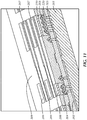
- the resist 208 is stripped and the dielectric 209 (e.g. SiO2) is deposited, followed by a polishing (CMP) step. The result thereof is shown in FIG. 9 .
- the dielectric 209 e.g. SiO2
- the metal of the gate contact and the metal of the contact line are not supposed to be cut at the same time. This can for example be the case in the middle of the cell where gates are continuous and then the contacts have to be separated for nMOS and pMOS. In that case after spinning the resist 208 a different mask can be printed. This mask can have different shapes. Only the chemistry that opens the dielectric cap 206 on the contact metal may for example be applied while the gate dielectric cap remains unaffected. Using the third chemistry the metal of the contact lines 210 is etched. The result thereof is shown in FIG. 10 showing the contact line cuts 230, the unaffected gate cap material 207, and the contact line cut 230. Next the resist is removed and the dielectric 209 (e.g. SiO2) is applied and polished (CMP). The result thereof is shown in FIG. 11 . Thus, a device can be obtained wherein the contact lines are only present over some of the fins. Some of the fins may for example only be covered by the ILD dielectric.
- a fin cut may be done after obtaining the at least one metal gate.
- the following process steps may be done to obtain such a fin cut.
- Apply a spin resist 208 expose the resist after having applied a mask, etchback the fin material (e.g. silicon) at the position 211 where the fin should be cut, remove the resist 208, deposit and polish the dielectric (e.g. SiO2).
- the dielectric 209 e.g. SiO2
- CMP polished
- interruptions to the gate contacts and to the contact lines are postponed to the point where both are metallized and capped each with a different cap material (as required for self-aligned gate contact SAGC further downstream).
- Interruptions to the gate contacts and to the contact lines can be made differentially by opening of the 2 cap materials and subsequently performing a metal etch of the gate contact or of the contact line.
- a fin cut is done after obtaining the at least one metal gate. Therefore, S/D epi grown on non-interrupted fins can be removed selectively opening the ILD0 oxide over the epi (selective to the plugs over gate and contact) and subsequently removing the S/D epi and fin.
- Interruptions may be filled back with dielectric, followed by CMP step in a single or multiple steps.
Landscapes
- Semiconductor Memories (AREA)
- Electrodes Of Semiconductors (AREA)
- Metal-Oxide And Bipolar Metal-Oxide Semiconductor Integrated Circuits (AREA)
Priority Applications (3)
| Application Number | Priority Date | Filing Date | Title |
|---|---|---|---|
| EP18193824.2A EP3624178A1 (fr) | 2018-09-11 | 2018-09-11 | Procédé de découpe de grille, de contact et d'ailette |
| CN201910549617.1A CN110890276A (zh) | 2018-09-11 | 2019-06-24 | 栅极、触点和翅片切割方法 |
| US16/567,485 US20200083116A1 (en) | 2018-09-11 | 2019-09-11 | Gate, Contact, and Fin Cut Method |
Applications Claiming Priority (1)
| Application Number | Priority Date | Filing Date | Title |
|---|---|---|---|
| EP18193824.2A EP3624178A1 (fr) | 2018-09-11 | 2018-09-11 | Procédé de découpe de grille, de contact et d'ailette |
Publications (1)
| Publication Number | Publication Date |
|---|---|
| EP3624178A1 true EP3624178A1 (fr) | 2020-03-18 |
Family
ID=63578983
Family Applications (1)
| Application Number | Title | Priority Date | Filing Date |
|---|---|---|---|
| EP18193824.2A Withdrawn EP3624178A1 (fr) | 2018-09-11 | 2018-09-11 | Procédé de découpe de grille, de contact et d'ailette |
Country Status (3)
| Country | Link |
|---|---|
| US (1) | US20200083116A1 (fr) |
| EP (1) | EP3624178A1 (fr) |
| CN (1) | CN110890276A (fr) |
Cited By (1)
| Publication number | Priority date | Publication date | Assignee | Title |
|---|---|---|---|---|
| EP3989273A1 (fr) * | 2020-10-20 | 2022-04-27 | Imec VZW | Procédé de formation d'un dispositif à semiconducteur et dispositif à semiconducteur |
Families Citing this family (2)
| Publication number | Priority date | Publication date | Assignee | Title |
|---|---|---|---|---|
| US11908910B2 (en) * | 2020-10-27 | 2024-02-20 | Taiwan Semiconductor Manufacturing Company, Ltd. | Semiconductor device having embedded conductive line and method of fabricating thereof |
| KR102916530B1 (ko) | 2022-04-20 | 2026-01-21 | 삼성전자 주식회사 | 집적회로 소자 |
Citations (5)
| Publication number | Priority date | Publication date | Assignee | Title |
|---|---|---|---|---|
| US20140077305A1 (en) * | 2012-09-19 | 2014-03-20 | Abhijit Jayant Pethe | Gate contact structure over active gate and method to fabricate same |
| US20140339610A1 (en) * | 2013-05-14 | 2014-11-20 | Globalfoundries Inc. | Finfet device and method of fabrication |
| US20150348965A1 (en) * | 2014-05-29 | 2015-12-03 | Taiwan Semiconductor Manufacturing Co., Ltd. | Structure and formation method of semiconductor device structure with metal gate |
| US9520482B1 (en) * | 2015-11-13 | 2016-12-13 | Taiwan Semiconductor Manufacturing Company, Ltd. | Method of cutting metal gate |
| US20180182859A1 (en) * | 2016-12-22 | 2018-06-28 | Taiwan Semiconductor Manufacturing Co., Ltd. | Metal gate structure and methods thereof |
Family Cites Families (1)
| Publication number | Priority date | Publication date | Assignee | Title |
|---|---|---|---|---|
| US8975712B2 (en) * | 2013-05-14 | 2015-03-10 | Globalfoundries Inc. | Densely packed standard cells for integrated circuit products, and methods of making same |
-
2018
- 2018-09-11 EP EP18193824.2A patent/EP3624178A1/fr not_active Withdrawn
-
2019
- 2019-06-24 CN CN201910549617.1A patent/CN110890276A/zh not_active Withdrawn
- 2019-09-11 US US16/567,485 patent/US20200083116A1/en not_active Abandoned
Patent Citations (5)
| Publication number | Priority date | Publication date | Assignee | Title |
|---|---|---|---|---|
| US20140077305A1 (en) * | 2012-09-19 | 2014-03-20 | Abhijit Jayant Pethe | Gate contact structure over active gate and method to fabricate same |
| US20140339610A1 (en) * | 2013-05-14 | 2014-11-20 | Globalfoundries Inc. | Finfet device and method of fabrication |
| US20150348965A1 (en) * | 2014-05-29 | 2015-12-03 | Taiwan Semiconductor Manufacturing Co., Ltd. | Structure and formation method of semiconductor device structure with metal gate |
| US9520482B1 (en) * | 2015-11-13 | 2016-12-13 | Taiwan Semiconductor Manufacturing Company, Ltd. | Method of cutting metal gate |
| US20180182859A1 (en) * | 2016-12-22 | 2018-06-28 | Taiwan Semiconductor Manufacturing Co., Ltd. | Metal gate structure and methods thereof |
Cited By (2)
| Publication number | Priority date | Publication date | Assignee | Title |
|---|---|---|---|---|
| EP3989273A1 (fr) * | 2020-10-20 | 2022-04-27 | Imec VZW | Procédé de formation d'un dispositif à semiconducteur et dispositif à semiconducteur |
| US12154832B2 (en) | 2020-10-20 | 2024-11-26 | Imec Vzw | Method for forming a semiconductor device and a semiconductor device |
Also Published As
| Publication number | Publication date |
|---|---|
| US20200083116A1 (en) | 2020-03-12 |
| CN110890276A (zh) | 2020-03-17 |
Similar Documents
| Publication | Publication Date | Title |
|---|---|---|
| US12453164B2 (en) | Dielectric fins with different dielectric constants and sizes in different regions of a semiconductor device | |
| US12033898B2 (en) | Method of fabricating a FinFET device | |
| US11081394B2 (en) | Method of making a FinFET device | |
| US10453843B2 (en) | Multiple finFET Formation with epitaxy separation | |
| US9196543B2 (en) | Structure and method for finFET device | |
| US9000522B2 (en) | FinFET with dielectric isolation by silicon-on-nothing and method of fabrication | |
| US9443768B2 (en) | Method of making a FinFET device | |
| US8975129B1 (en) | Method of making a FinFET device | |
| US9147612B2 (en) | Method for forming a semiconductor structure | |
| US9954104B2 (en) | Multiwidth finFET with channel cladding | |
| KR101996134B1 (ko) | 소스/드레인 에피택시 영역들을 위한 유연한 병합 기법 | |
| KR102042718B1 (ko) | 핀 전계 효과 트랜지스터 디바이스 및 방법 | |
| CN108010967A (zh) | 制造具有改进的漏极中的金属落置的esd finfet的系统和方法 | |
| EP3624178A1 (fr) | Procédé de découpe de grille, de contact et d'ailette | |
| TW202213625A (zh) | 用於製造先進積體電路結構之閘極與鰭片微調隔離 | |
| TW201725629A (zh) | 半導體元件及其製作方法 | |
| US20250301704A1 (en) | Semiconductor device including gate-cut structure formed at early step of manufacturing process | |
| US10950505B2 (en) | Multiple finFET formation with epitaxy separation |
Legal Events
| Date | Code | Title | Description |
|---|---|---|---|
| PUAI | Public reference made under article 153(3) epc to a published international application that has entered the european phase |
Free format text: ORIGINAL CODE: 0009012 |
|
| STAA | Information on the status of an ep patent application or granted ep patent |
Free format text: STATUS: THE APPLICATION HAS BEEN PUBLISHED |
|
| AK | Designated contracting states |
Kind code of ref document: A1 Designated state(s): AL AT BE BG CH CY CZ DE DK EE ES FI FR GB GR HR HU IE IS IT LI LT LU LV MC MK MT NL NO PL PT RO RS SE SI SK SM TR |
|
| AX | Request for extension of the european patent |
Extension state: BA ME |
|
| STAA | Information on the status of an ep patent application or granted ep patent |
Free format text: STATUS: THE APPLICATION IS DEEMED TO BE WITHDRAWN |
|
| 18D | Application deemed to be withdrawn |
Effective date: 20200919 |