EP3624200A1 - Germaniumreicher nanodrahttransistor mit entspannter pufferschicht - Google Patents
Germaniumreicher nanodrahttransistor mit entspannter pufferschicht Download PDFInfo
- Publication number
- EP3624200A1 EP3624200A1 EP19183091.8A EP19183091A EP3624200A1 EP 3624200 A1 EP3624200 A1 EP 3624200A1 EP 19183091 A EP19183091 A EP 19183091A EP 3624200 A1 EP3624200 A1 EP 3624200A1
- Authority
- EP
- European Patent Office
- Prior art keywords
- layer
- germanium
- substrate
- silicon
- source
- Prior art date
- Legal status (The legal status is an assumption and is not a legal conclusion. Google has not performed a legal analysis and makes no representation as to the accuracy of the status listed.)
- Granted
Links
Images


Classifications
-
- H—ELECTRICITY
- H10—SEMICONDUCTOR DEVICES; ELECTRIC SOLID-STATE DEVICES NOT OTHERWISE PROVIDED FOR
- H10D—INORGANIC ELECTRIC SEMICONDUCTOR DEVICES
- H10D62/00—Semiconductor bodies, or regions thereof, of devices having potential barriers
- H10D62/10—Shapes, relative sizes or dispositions of the regions of the semiconductor bodies; Shapes of the semiconductor bodies
- H10D62/117—Shapes of semiconductor bodies
- H10D62/118—Nanostructure semiconductor bodies
- H10D62/119—Nanowire, nanosheet or nanotube semiconductor bodies
- H10D62/121—Nanowire, nanosheet or nanotube semiconductor bodies oriented parallel to substrates
-
- H—ELECTRICITY
- H10—SEMICONDUCTOR DEVICES; ELECTRIC SOLID-STATE DEVICES NOT OTHERWISE PROVIDED FOR
- H10D—INORGANIC ELECTRIC SEMICONDUCTOR DEVICES
- H10D30/00—Field-effect transistors [FET]
- H10D30/01—Manufacture or treatment
- H10D30/019—Manufacture or treatment of FETs having stacked nanowire, nanosheet or nanoribbon channels
-
- H—ELECTRICITY
- H10—SEMICONDUCTOR DEVICES; ELECTRIC SOLID-STATE DEVICES NOT OTHERWISE PROVIDED FOR
- H10D—INORGANIC ELECTRIC SEMICONDUCTOR DEVICES
- H10D30/00—Field-effect transistors [FET]
- H10D30/01—Manufacture or treatment
- H10D30/021—Manufacture or treatment of FETs having insulated gates [IGFET]
- H10D30/031—Manufacture or treatment of FETs having insulated gates [IGFET] of thin-film transistors [TFT]
-
- H—ELECTRICITY
- H10—SEMICONDUCTOR DEVICES; ELECTRIC SOLID-STATE DEVICES NOT OTHERWISE PROVIDED FOR
- H10D—INORGANIC ELECTRIC SEMICONDUCTOR DEVICES
- H10D30/00—Field-effect transistors [FET]
- H10D30/501—FETs having stacked nanowire, nanosheet or nanoribbon channels
-
- H—ELECTRICITY
- H10—SEMICONDUCTOR DEVICES; ELECTRIC SOLID-STATE DEVICES NOT OTHERWISE PROVIDED FOR
- H10D—INORGANIC ELECTRIC SEMICONDUCTOR DEVICES
- H10D30/00—Field-effect transistors [FET]
- H10D30/60—Insulated-gate field-effect transistors [IGFET]
- H10D30/62—Fin field-effect transistors [FinFET]
- H10D30/6211—Fin field-effect transistors [FinFET] having fin-shaped semiconductor bodies integral with the bulk semiconductor substrates
-
- H—ELECTRICITY
- H10—SEMICONDUCTOR DEVICES; ELECTRIC SOLID-STATE DEVICES NOT OTHERWISE PROVIDED FOR
- H10D—INORGANIC ELECTRIC SEMICONDUCTOR DEVICES
- H10D30/00—Field-effect transistors [FET]
- H10D30/60—Insulated-gate field-effect transistors [IGFET]
- H10D30/67—Thin-film transistors [TFT]
- H10D30/6704—Thin-film transistors [TFT] having supplementary regions or layers in the thin films or in the insulated bulk substrates for controlling properties of the device
- H10D30/6713—Thin-film transistors [TFT] having supplementary regions or layers in the thin films or in the insulated bulk substrates for controlling properties of the device characterised by the properties of the source or drain regions, e.g. compositions or sectional shapes
-
- H—ELECTRICITY
- H10—SEMICONDUCTOR DEVICES; ELECTRIC SOLID-STATE DEVICES NOT OTHERWISE PROVIDED FOR
- H10D—INORGANIC ELECTRIC SEMICONDUCTOR DEVICES
- H10D30/00—Field-effect transistors [FET]
- H10D30/60—Insulated-gate field-effect transistors [IGFET]
- H10D30/67—Thin-film transistors [TFT]
- H10D30/6729—Thin-film transistors [TFT] characterised by the electrodes
- H10D30/673—Thin-film transistors [TFT] characterised by the electrodes characterised by the shapes, relative sizes or dispositions of the gate electrodes
- H10D30/6735—Thin-film transistors [TFT] characterised by the electrodes characterised by the shapes, relative sizes or dispositions of the gate electrodes having gates fully surrounding the channels, e.g. gate-all-around
-
- H—ELECTRICITY
- H10—SEMICONDUCTOR DEVICES; ELECTRIC SOLID-STATE DEVICES NOT OTHERWISE PROVIDED FOR
- H10D—INORGANIC ELECTRIC SEMICONDUCTOR DEVICES
- H10D30/00—Field-effect transistors [FET]
- H10D30/60—Insulated-gate field-effect transistors [IGFET]
- H10D30/67—Thin-film transistors [TFT]
- H10D30/674—Thin-film transistors [TFT] characterised by the active materials
- H10D30/6741—Group IV materials, e.g. germanium or silicon carbide
-
- H—ELECTRICITY
- H10—SEMICONDUCTOR DEVICES; ELECTRIC SOLID-STATE DEVICES NOT OTHERWISE PROVIDED FOR
- H10D—INORGANIC ELECTRIC SEMICONDUCTOR DEVICES
- H10D30/00—Field-effect transistors [FET]
- H10D30/60—Insulated-gate field-effect transistors [IGFET]
- H10D30/67—Thin-film transistors [TFT]
- H10D30/6757—Thin-film transistors [TFT] characterised by the structure of the channel, e.g. transverse or longitudinal shape or doping profile
-
- H—ELECTRICITY
- H10—SEMICONDUCTOR DEVICES; ELECTRIC SOLID-STATE DEVICES NOT OTHERWISE PROVIDED FOR
- H10D—INORGANIC ELECTRIC SEMICONDUCTOR DEVICES
- H10D30/00—Field-effect transistors [FET]
- H10D30/60—Insulated-gate field-effect transistors [IGFET]
- H10D30/67—Thin-film transistors [TFT]
- H10D30/6758—Thin-film transistors [TFT] characterised by the insulating substrates
-
- H—ELECTRICITY
- H10—SEMICONDUCTOR DEVICES; ELECTRIC SOLID-STATE DEVICES NOT OTHERWISE PROVIDED FOR
- H10D—INORGANIC ELECTRIC SEMICONDUCTOR DEVICES
- H10D30/00—Field-effect transistors [FET]
- H10D30/60—Insulated-gate field-effect transistors [IGFET]
- H10D30/791—Arrangements for exerting mechanical stress on the crystal lattice of the channel regions
- H10D30/797—Arrangements for exerting mechanical stress on the crystal lattice of the channel regions being in source or drain regions, e.g. SiGe source or drain
-
- H—ELECTRICITY
- H10—SEMICONDUCTOR DEVICES; ELECTRIC SOLID-STATE DEVICES NOT OTHERWISE PROVIDED FOR
- H10D—INORGANIC ELECTRIC SEMICONDUCTOR DEVICES
- H10D62/00—Semiconductor bodies, or regions thereof, of devices having potential barriers
- H10D62/10—Shapes, relative sizes or dispositions of the regions of the semiconductor bodies; Shapes of the semiconductor bodies
- H10D62/113—Isolations within a component, i.e. internal isolations
- H10D62/115—Dielectric isolations, e.g. air gaps
-
- H—ELECTRICITY
- H10—SEMICONDUCTOR DEVICES; ELECTRIC SOLID-STATE DEVICES NOT OTHERWISE PROVIDED FOR
- H10D—INORGANIC ELECTRIC SEMICONDUCTOR DEVICES
- H10D62/00—Semiconductor bodies, or regions thereof, of devices having potential barriers
- H10D62/10—Shapes, relative sizes or dispositions of the regions of the semiconductor bodies; Shapes of the semiconductor bodies
- H10D62/113—Isolations within a component, i.e. internal isolations
- H10D62/115—Dielectric isolations, e.g. air gaps
- H10D62/116—Dielectric isolations, e.g. air gaps adjoining the input or output regions of field-effect devices, e.g. adjoining source or drain regions
-
- H—ELECTRICITY
- H10—SEMICONDUCTOR DEVICES; ELECTRIC SOLID-STATE DEVICES NOT OTHERWISE PROVIDED FOR
- H10D—INORGANIC ELECTRIC SEMICONDUCTOR DEVICES
- H10D62/00—Semiconductor bodies, or regions thereof, of devices having potential barriers
- H10D62/10—Shapes, relative sizes or dispositions of the regions of the semiconductor bodies; Shapes of the semiconductor bodies
- H10D62/13—Semiconductor regions connected to electrodes carrying current to be rectified, amplified or switched, e.g. source or drain regions
- H10D62/149—Source or drain regions of field-effect devices
- H10D62/151—Source or drain regions of field-effect devices of IGFETs
-
- H—ELECTRICITY
- H10—SEMICONDUCTOR DEVICES; ELECTRIC SOLID-STATE DEVICES NOT OTHERWISE PROVIDED FOR
- H10D—INORGANIC ELECTRIC SEMICONDUCTOR DEVICES
- H10D62/00—Semiconductor bodies, or regions thereof, of devices having potential barriers
- H10D62/10—Shapes, relative sizes or dispositions of the regions of the semiconductor bodies; Shapes of the semiconductor bodies
- H10D62/17—Semiconductor regions connected to electrodes not carrying current to be rectified, amplified or switched, e.g. channel regions
- H10D62/213—Channel regions of field-effect devices
- H10D62/221—Channel regions of field-effect devices of FETs
-
- H—ELECTRICITY
- H10—SEMICONDUCTOR DEVICES; ELECTRIC SOLID-STATE DEVICES NOT OTHERWISE PROVIDED FOR
- H10D—INORGANIC ELECTRIC SEMICONDUCTOR DEVICES
- H10D62/00—Semiconductor bodies, or regions thereof, of devices having potential barriers
- H10D62/10—Shapes, relative sizes or dispositions of the regions of the semiconductor bodies; Shapes of the semiconductor bodies
- H10D62/17—Semiconductor regions connected to electrodes not carrying current to be rectified, amplified or switched, e.g. channel regions
- H10D62/351—Substrate regions of field-effect devices
- H10D62/357—Substrate regions of field-effect devices of FETs
- H10D62/364—Substrate regions of field-effect devices of FETs of IGFETs
-
- H—ELECTRICITY
- H10—SEMICONDUCTOR DEVICES; ELECTRIC SOLID-STATE DEVICES NOT OTHERWISE PROVIDED FOR
- H10D—INORGANIC ELECTRIC SEMICONDUCTOR DEVICES
- H10D62/00—Semiconductor bodies, or regions thereof, of devices having potential barriers
- H10D62/80—Semiconductor bodies, or regions thereof, of devices having potential barriers characterised by the materials
- H10D62/82—Heterojunctions
- H10D62/822—Heterojunctions comprising only Group IV materials heterojunctions, e.g. Si/Ge heterojunctions
-
- H—ELECTRICITY
- H10—SEMICONDUCTOR DEVICES; ELECTRIC SOLID-STATE DEVICES NOT OTHERWISE PROVIDED FOR
- H10D—INORGANIC ELECTRIC SEMICONDUCTOR DEVICES
- H10D62/00—Semiconductor bodies, or regions thereof, of devices having potential barriers
- H10D62/80—Semiconductor bodies, or regions thereof, of devices having potential barriers characterised by the materials
- H10D62/83—Semiconductor bodies, or regions thereof, of devices having potential barriers characterised by the materials being Group IV materials, e.g. B-doped Si or undoped Ge
- H10D62/832—Semiconductor bodies, or regions thereof, of devices having potential barriers characterised by the materials being Group IV materials, e.g. B-doped Si or undoped Ge being Group IV materials comprising two or more elements, e.g. SiGe
-
- H—ELECTRICITY
- H10—SEMICONDUCTOR DEVICES; ELECTRIC SOLID-STATE DEVICES NOT OTHERWISE PROVIDED FOR
- H10D—INORGANIC ELECTRIC SEMICONDUCTOR DEVICES
- H10D64/00—Electrodes of devices having potential barriers
- H10D64/01—Manufacture or treatment
- H10D64/017—Manufacture or treatment using dummy gates in processes wherein at least parts of the final gates are self-aligned to the dummy gates, i.e. replacement gate processes
-
- H—ELECTRICITY
- H10—SEMICONDUCTOR DEVICES; ELECTRIC SOLID-STATE DEVICES NOT OTHERWISE PROVIDED FOR
- H10D—INORGANIC ELECTRIC SEMICONDUCTOR DEVICES
- H10D64/00—Electrodes of devices having potential barriers
- H10D64/20—Electrodes characterised by their shapes, relative sizes or dispositions
- H10D64/27—Electrodes not carrying the current to be rectified, amplified, oscillated or switched, e.g. gates
- H10D64/311—Gate electrodes for field-effect devices
- H10D64/411—Gate electrodes for field-effect devices for FETs
- H10D64/511—Gate electrodes for field-effect devices for FETs for IGFETs
- H10D64/512—Disposition of the gate electrodes, e.g. buried gates
-
- H—ELECTRICITY
- H10—SEMICONDUCTOR DEVICES; ELECTRIC SOLID-STATE DEVICES NOT OTHERWISE PROVIDED FOR
- H10D—INORGANIC ELECTRIC SEMICONDUCTOR DEVICES
- H10D84/00—Integrated devices formed in or on semiconductor substrates that comprise only semiconducting layers, e.g. on Si wafers or on GaAs-on-Si wafers
- H10D84/01—Manufacture or treatment
- H10D84/0123—Integrating together multiple components covered by H10D12/00 or H10D30/00, e.g. integrating multiple IGBTs
- H10D84/0126—Integrating together multiple components covered by H10D12/00 or H10D30/00, e.g. integrating multiple IGBTs the components including insulated gates, e.g. IGFETs
- H10D84/0165—Integrating together multiple components covered by H10D12/00 or H10D30/00, e.g. integrating multiple IGBTs the components including insulated gates, e.g. IGFETs the components including complementary IGFETs, e.g. CMOS devices
- H10D84/0193—Integrating together multiple components covered by H10D12/00 or H10D30/00, e.g. integrating multiple IGBTs the components including insulated gates, e.g. IGFETs the components including complementary IGFETs, e.g. CMOS devices the components including FinFETs
-
- H—ELECTRICITY
- H10—SEMICONDUCTOR DEVICES; ELECTRIC SOLID-STATE DEVICES NOT OTHERWISE PROVIDED FOR
- H10D—INORGANIC ELECTRIC SEMICONDUCTOR DEVICES
- H10D84/00—Integrated devices formed in or on semiconductor substrates that comprise only semiconducting layers, e.g. on Si wafers or on GaAs-on-Si wafers
- H10D84/01—Manufacture or treatment
- H10D84/02—Manufacture or treatment characterised by using material-based technologies
- H10D84/03—Manufacture or treatment characterised by using material-based technologies using Group IV technology, e.g. silicon technology or silicon-carbide [SiC] technology
- H10D84/038—Manufacture or treatment characterised by using material-based technologies using Group IV technology, e.g. silicon technology or silicon-carbide [SiC] technology using silicon technology, e.g. SiGe
-
- B—PERFORMING OPERATIONS; TRANSPORTING
- B82—NANOTECHNOLOGY
- B82Y—SPECIFIC USES OR APPLICATIONS OF NANOSTRUCTURES; MEASUREMENT OR ANALYSIS OF NANOSTRUCTURES; MANUFACTURE OR TREATMENT OF NANOSTRUCTURES
- B82Y10/00—Nanotechnology for information processing, storage or transmission, e.g. quantum computing or single electron logic
-
- H—ELECTRICITY
- H10—SEMICONDUCTOR DEVICES; ELECTRIC SOLID-STATE DEVICES NOT OTHERWISE PROVIDED FOR
- H10D—INORGANIC ELECTRIC SEMICONDUCTOR DEVICES
- H10D30/00—Field-effect transistors [FET]
- H10D30/60—Insulated-gate field-effect transistors [IGFET]
- H10D30/62—Fin field-effect transistors [FinFET]
- H10D30/6219—Fin field-effect transistors [FinFET] characterised by the source or drain electrodes
-
- H—ELECTRICITY
- H10—SEMICONDUCTOR DEVICES; ELECTRIC SOLID-STATE DEVICES NOT OTHERWISE PROVIDED FOR
- H10D—INORGANIC ELECTRIC SEMICONDUCTOR DEVICES
- H10D84/00—Integrated devices formed in or on semiconductor substrates that comprise only semiconducting layers, e.g. on Si wafers or on GaAs-on-Si wafers
- H10D84/01—Manufacture or treatment
- H10D84/0123—Integrating together multiple components covered by H10D12/00 or H10D30/00, e.g. integrating multiple IGBTs
- H10D84/0126—Integrating together multiple components covered by H10D12/00 or H10D30/00, e.g. integrating multiple IGBTs the components including insulated gates, e.g. IGFETs
- H10D84/0165—Integrating together multiple components covered by H10D12/00 or H10D30/00, e.g. integrating multiple IGBTs the components including insulated gates, e.g. IGFETs the components including complementary IGFETs, e.g. CMOS devices
- H10D84/0167—Manufacturing their channels
-
- H—ELECTRICITY
- H10—SEMICONDUCTOR DEVICES; ELECTRIC SOLID-STATE DEVICES NOT OTHERWISE PROVIDED FOR
- H10D—INORGANIC ELECTRIC SEMICONDUCTOR DEVICES
- H10D84/00—Integrated devices formed in or on semiconductor substrates that comprise only semiconducting layers, e.g. on Si wafers or on GaAs-on-Si wafers
- H10D84/80—Integrated devices formed in or on semiconductor substrates that comprise only semiconducting layers, e.g. on Si wafers or on GaAs-on-Si wafers characterised by the integration of at least one component covered by groups H10D12/00 or H10D30/00, e.g. integration of IGFETs
- H10D84/82—Integrated devices formed in or on semiconductor substrates that comprise only semiconducting layers, e.g. on Si wafers or on GaAs-on-Si wafers characterised by the integration of at least one component covered by groups H10D12/00 or H10D30/00, e.g. integration of IGFETs of only field-effect components
- H10D84/83—Integrated devices formed in or on semiconductor substrates that comprise only semiconducting layers, e.g. on Si wafers or on GaAs-on-Si wafers characterised by the integration of at least one component covered by groups H10D12/00 or H10D30/00, e.g. integration of IGFETs of only field-effect components of only insulated-gate FETs [IGFET]
- H10D84/85—Complementary IGFETs, e.g. CMOS
Definitions
- a field-effect transistor is a semiconductor device that includes three terminals: a gate, a source, and a drain.
- a FET uses an electric field applied by the gate to control the electrical conductivity of a channel through which charge carriers (e.g., electrons or holes) flow between the source and drain.
- charge carriers e.g., electrons or holes
- the FET is referred to as an n-channel device
- the FET is referred to as a p-channel device.
- MOSFETs metal-oxide-semiconductor FETs
- MOSFETs include a gate dielectric between the gate and the channel.
- MOSFETs may also be known as metal-insulator-semiconductor FETs (MISFETSs) or insulated-gate FETs (IGFETs).
- MISFETSs metal-insulator-semiconductor FETs
- IGFETs insulated-gate FETs
- Complementary MOS (CMOS) structures use a combination of p-channel MOSFET (PMOS) and n-channel MOSFET (NMOS) devices to implement logic gates and other digital circuits.
- PMOS p-channel MOSFET
- NMOS n-channel MOSFET
- a FinFET is a MOSFET transistor built around a thin strip of semiconductor material (generally referred to as a fin).
- the conductive channel of the FinFET device resides on the outer portions of the fin adjacent to the gate dielectric. Specifically, current runs along/within both sidewalls of the fin (sides perpendicular to the substrate surface) as well as along the top of the fin (side parallel to the substrate surface). Because the conductive channel of such configurations includes three different planer regions of the fin (e.g., top and two sides), such a FinFET design is sometimes referred to as a tri-gate transistor.
- a nanowire transistor (sometimes referred to as a gate-all-around (GAA) or nanoribbon transistor) is configured similarly to a fin-based transistor, but instead of a finned channel region with the gate in contact with three sides of the fin, one or more nanowires extend between the source and the drain regions.
- GAA gate-all-around
- the gate material generally surrounds or encircles each nanowire (hence, gate-all-around).
- a semiconductor structure includes a base layer or substrate comprising silicon.
- a relatively thin layer of relaxed buffer material is on the substrate.
- the relaxed buffer material has a thickness no greater than 200 to 300 nm.
- the relaxed buffer material comprises silicon and germanium with a germanium concentration from 20 to 45 atomic percent.
- the relaxed buffer layer material relaxes from 70 to 100% relative to the substrate. In some embodiments, the relaxation is at last 75%.
- the relaxed buffer material functions as a virtual substrate for subsequently formed materials in the device.
- the transistor structure includes a source and a drain.
- a body of monocrystalline silicon germanium (SiGe) extends between the source and drain and has a germanium concentration of at least 30 atomic percent.
- the body is a nanowire, nanoribbon, or nanosheet of monocrystalline SiGe.
- the body has a germanium concentration from 30 to 85 atomic percent.
- a gate structure is wrapped around the body and includes a gate dielectric and a gate electrode, where the gate dielectric is between the body and the gate electrode.
- the nanowires/nanoribbons/nanosheets are strained to the relaxed buffer material as analyzed by transmission electron spectroscopy (TEM). Due to relaxation of the buffer material, defects can be observed at the interface between the silicon substrate and the SiGe buffer material, where the defects originate at the interface between the substrate and the relaxed buffer material and terminate in the silicon substrate below. As such, the relaxed buffer material is nominally free of defects and serves as a template for strained SiGe.
- TEM transmission electron spectroscopy
- the transistor structure includes a layer of isolation material below the source and/or drain (S/D), such as between the relaxed buffer material and the S/D material.
- the isolation material is useful to prevent or reduce leakage between the source and drain via the relaxed buffer or the substrate material (e.g., Silicon).
- the substrate may exhibit implant damage in the lattice due to implantation.
- the substrate and/or relaxed buffer material comprise carbon, arsenic, hydrogen, helium, or nitrogen in some embodiments.
- the source and drain are processed to include an end portion adjacent the channel that reduces or prevents diffusion of phosphorous used as a dopant.
- the end portion can be epitaxial material that is rich in germanium (e.g., up to 100% germanium), SiGe that includes up to 4% carbon (SiGeC), or germanium compounds that include tin (e.g., SiGeSn and GeSn alloys).
- the NMOS transistor has a silicon channel
- the PMOS transistor has a SiGe channel with germanium greater than 30%.
- the transistor devices can be nanowire or TFET devices, for example.
- any compressively-strained material including indium gallium arsenide (InGaAs), antimonides, or any heteroepitaxial material that is difficult to grow on a silicon substrate, for example.
- InGaAs indium gallium arsenide
- Using a relaxed buffer material with 20-45% Ge accomplishes the goal of maintaining strain in the nanowire below a critical value where the wire would relax plastically.
- Such material has a germanium concentration that bridges the gap in lattice constants between the substrate and the channel material, but does not completely eliminate strain, in accordance with some embodiments.
- misfit dislocations are present below the interface between the relaxed buffer material and the silicon substrate.
- the relaxed buffer material above is nominally free of defects and has a relaxed lattice constant. Numerous variations and embodiments will be apparent in light of the present disclosure.
- the GAA channel region can have one or more nanowires extending between the source and drain regions, such as a vertical stack of nanowires that extend horizontally between the source and drain regions.
- the gate structure wraps around the nanowire(s).
- alternating layers of silicon (Si) and silicon germanium (SiGe) are formed epitaxially on a bulk silicon substrate. Etching down into the layer stack defines one or more fins that include a silicon subfin and alternating layers of SiGe and Si on top of the subfin.
- CMOS transistor structure can be formed with silicon nanowires in n-MOS devices and SiGe channel in p-MOS devices.
- both n-MOS and p-MOS devices have silicon wire channels.
- both n-MOS and p-MOS devices have SiGe wire channels.
- SiGe structures formed on Si may exhibit misfit dislocations and other faults due to lattice mismatch between the materials.
- SiGe has an atomic germanium content greater than 30% and thickness greater than a few hundred angstroms, for example, the lattice may relax to form misfit dislocations that are detrimental to device performance.
- Fabricating high quality SiGe nanowire devices with a germanium concentration of 40% or more typically requires nominally defect-free channel regions. Relaxation structures can be used to avoid or reduce dislocations, such as a layer of SiGe with the Ge concentration graded over a thickness of 2 to 10 ⁇ m.
- relaxation structures with a thickness greater than 1 ⁇ m are not amenable to high-volume manufacturing due to high costs of material and energy, low throughput, and short chamber life, among other challenges. Wafer bonding and other techniques are available, but also are not amendable to high-volume manufacturing. Another challenge is current leakage through the substrate between the source and drain. Further challenges include dopant diffusion and unintentional damage to SiGe S/D regions when removing the silicon between SiGe nanowires.
- techniques are provided for forming a SiGe channel structure that employs a thin relaxation layer (e.g., ⁇ 300 nm).
- a layer stack of Si and SiGe is formed on the relaxation layer, followed by processing the layer stack into fins, and then into nanowire transistors.
- the layer stack is nominally free of defects and the materials in the layer stack have relaxed lattice constants.
- the relaxation layer serves as a relaxed buffer layer for a compressively-strained SiGe channel PMOS transistor and tensile-strained Si channel NMOS transistor simultaneously.
- the relaxed buffer layer is SiGe with germanium concentration from 20 to 45 at% that is at least 75% relaxed.
- a layer stack of Si and SiGe is formed, followed by processing to define nanowire, nanoribbons, or nanosheets that are defect-free and have relaxed lattice constants.
- a device having a channel with multiple nanowires or nanoribbons can be fabricated, where the channel material is SiGe with up to 85 at% Ge.
- a sacrificial layer is added onto the top of the relaxed buffer layer, followed by depositing the layer stack of Si and SiGe. After forming the transistor structure, the sacrificial layer can be removed and replaced with isolation material. The resulting structure includes an isolation layer below the source and drain.
- one embodiment according to the present disclosure utilizes SiGe source and drain regions having low Ge content for n-MOS devices.
- tin can be added to the SiGe to provide strain equivalent to a SiGe material having ⁇ 50 at% Ge.
- the resulting structure includes an epitaxial S/D structure.
- epitaxial n-type S/D regions can prevent or reduce phosphorous diffusion by using a carbon-rich layer in the end portion of the S/D adjacent the channel region.
- SiGe etchout in the S/D can be minimized by using Ge-rich regions at the tip of the S/D adjacent the channel region, so that when Si is etched out of the layer stack in the channel region, the epitaxial SiGe in the S/D does not get unintentionally damaged.
- the S/D includes an end portion with up to 4% carbon and/or a high germanium content.
- the end portion includes tin, such as an alloy of SiGeSn or GeSn.
- the presence of interface processing can be identified by the presence of defects (dislocations stacking and faults) that begin at the Si substrate-SiGe buffer interface but terminate in the substrate material below the relaxed buffer region. Such defects can be detected using through TEM imaging.
- the relaxed buffer layer can include one or more of Si, Ge, C, Ar, H, He, or N.
- the elements in the relaxed buffer layer can be identified via SIMS, TEM EDX mapping, or Atom Probe Tomography. Signatures of long range implant damage below the Si substrate-SiGe buffer interface can be detected TEM imaging. Such signatures may include lattice damage that is indicative of an ion implantation process to form the relaxed buffer layer.
- the relaxed buffer layer thus fabricated could serve as the template for Si or SiGe channel CMOS transistors either via film deposition plus fin patterning, or through the aspect-ratio-trapping (ART) approach within trenches.
- the relaxed buffer could also serve as the template for fabricating nanowire or TFET transistors.
- the process flow can be gate first or gate last.
- the source/drain (S/D) can be formed either via etch plus fill or through a raised S/D approach.
- nanowire is not limited to structures of a particular cross-sectional shape, but includes structures of a rectangular, square, trapezoidal, "racetrack” (e.g., parallel sides connected by rounded ends), circular, oval, elongated, and other cross-sectional shapes, some of which may be referred to as nanoribbons or nanosheets.
- a nanowire is a structure that has a thickness or diameter on the order of tens of nanometers or less, and an unconstrained length.
- group IV semiconductor material includes at least one group IV element (e.g., silicon, germanium, carbon, tin), such as silicon (Si), germanium (Ge), silicon-germanium (SiGe), and so forth.
- group III-V semiconductor material includes at least one group III element (e.g., aluminum, gallium, indium) and at least one group V element (e.g., nitrogen, phosphorus, arsenic, antimony, bismuth), such as gallium arsenide
- group III may also be known as the boron group or IUPAC group 13
- group IV may also be known as the carbon group or IUPAC group 14
- group V may also be known as the nitrogen family or IUPAC group 15, for example.
- compositionally different refers to two materials that have different chemical compositions. This compositional difference may be, for instance, by virtue of an element that is in one material but not the other (e.g., SiGe is compositionally different from silicon), or by way of one material having all the same elements as a second material but at least one of those elements is intentionally provided at a different concentration in one material relative to the other material (e.g., SiGe having 70 atomic percent germanium is compositionally different from SiGe having 25 atomic percent germanium).
- the materials may also have distinct dopants (e.g., gallium and magnesium) or the same dopants but at differing concentrations.
- compositionally distinct materials may further refer to two materials that have different crystallographic orientations. For instance, (110) silicon is compositionally distinct or different from (100) silicon.
- source/drain herein is simply intended to refer to a source region or a drain region or both a source region and a drain region.
- Source/drain is abbreviated S/D.
- the forward slash as used herein means “and/or” unless otherwise specified and is not intended to implicate any particular structural limitation or arrangement with respect to source and drain regions, or any other materials or features that are listed herein in conjunction with a forward slash.
- the techniques described herein can be used to benefit n-channel devices (e.g., NMOS) and/or p-channel devices (e.g., PMOS).
- the techniques described herein can be used to form complementary transistor circuits (such as CMOS circuits), where the techniques can be used to benefit one or more of the included n-channel and p-channel transistors making up the CMOS circuit.
- CMOS circuits complementary transistor circuits
- SiGe may be used in the channel of one or more PMOS devices and Si may be used in the channel of one or more NMOS devices.
- the techniques described herein can be used to benefit MOSFET devices, FinFET devices, and/or any other suitable devices as will be apparent in light of this disclosure. Further yet, in some embodiments, the techniques described herein can be used to benefit a multitude of transistor configurations, such as planar and non-planar configurations, where the non-planar configurations may include finned or FinFET configurations (e.g., dual-gate or tri-gate), gate-all-around (GAA) configurations (e.g., nanowire or nanoribbon), or some combination thereof (e.g., beaded-fin configurations), to provide a few examples.
- FinFET configurations e.g., dual-gate or tri-gate
- GAA gate-all-around
- nanowire or nanoribbon e.g., nanowire or nanoribbon
- beaded-fin configurations e.g., beaded-fin configurations
- the techniques can be used for a variety of source/drain (S/D) configurations, such as replacement material S/D, cladded S/D, and/or any other suitable S/D configuration as will be apparent in light of this disclosure.
- S/D source/drain
- the techniques described herein may be used to benefit logic transistor devices or transistor-based devices used for other suitable applications (e.g., amplification, switching, etc.). Therefore, the techniques described herein can be used to benefit a multitude of transistor devices.
- the techniques allow transistors to be further scaled with diverse channel materials, while ensuring higher operating voltage, higher drive currents, and thereby improved performance.
- any such devices may employ semiconductor materials that are three-dimensional crystals as well as two dimensional crystals or nanotubes, for example.
- the techniques may be used to benefit devices of varying scales, such as IC devices having critical dimensions in the micrometer (micron) range and/or in the nanometer (nm) range (e.g., formed at the 22, 14, 10, 7, 5, or 3 nm process nodes, or beyond).
- Use of the techniques and structures provided herein may be detectable using tools such as electron microscopy including scanning/transmission electron microscopy (SEM/TEM), scanning transmission electron microscopy (STEM), nano-beam electron diffraction (NBD or NBED), and reflection electron microscopy (REM); composition mapping; x-ray crystallography or diffraction (XRD); energy-dispersive x-ray spectroscopy (EDX); secondary ion mass spectrometry (SIMS); time-of-flight SIMS (ToF-SIMS); atom probe imaging or tomography; local electrode atom probe (LEAP) techniques; 3D tomography; or high resolution physical or chemical analysis, to name a few suitable example analytical tools.
- tools such as electron microscopy including scanning/transmission electron microscopy (SEM/TEM), scanning transmission electron microscopy (STEM), nano-beam electron diffraction (NBD or NBED), and reflection electron microscopy (REM); composition mapping; x-ray crystallography or
- such tools may indicate a transistor with a nanowire channel region of SiGe having a germanium concentration of 40 at% or more.
- such tools can be used to detect, a Ge-rich SiGe channel material that is free of defects and has a relaxed lattice constant.
- TEM can be useful to show a cross section of the device structure.
- x-ray crystallography can be useful to illustrate the crystal quality of the active channel material. X-ray crystallography may be used to illustrate the presence of germanium in the end portions of a nanowire, but a body portion that is free of germanium.
- the techniques described herein may be detected based on the benefits derived from their use, which includes channel materials with improved shapes, reduced impurities, improved carrier mobility, relatively higher operating voltage, relatively higher drive currents, and/or other improved device performance. Numerous configurations and variations will be apparent in light of this disclosure.
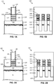
- FIGS. 1A and 1B illustrate cross-sectional views of a nanowire transistor structure 100 in accordance with an embodiment of the present disclosure, where FIG. 1A is a section taken through the channel region 130 of one device, such as along line C-C of FIG. 12 .
- FIG. 1B is a section taken through the gate structure 140 and perpendicular to the channel regions 130 of three devices, such as along line B-B of FIG. 12 .
- the transistor structure 100 includes a base layer or substrate 110, such as single-crystal silicon or other suitable semiconductor material.
- a relatively thin and layer of relaxed buffer material 112 is on the substrate 110.
- the relaxed buffer material 112 is Si 1-x Ge x with x from 0.2 to 0.45, where the SiGe is at least 75% relaxed relative to the substrate 110.
- the buffer material 112 has a thickness not greater than 300 nm, including 200 nm or less.
- Source and drain regions 120 are formed on the relaxed buffer material 112 and in contact with opposite sides of a channel region 130.
- the channel region 130 is formed initially on the relaxed buffer material 112 as a layer stack of alternating materials.
- the channel region 130 has a layer stack with alternating layers of nominally defect-free Si and SiGe.
- the Si exhibits tensile strain and the SiGe exhibits compressive strain in the layer stack, but the remaining material in the channel region 130 has a relaxed lattice constant after releasing the nanowires.
- the SiGe relaxes from 70% to 100% relative to the Si after releasing the nanowires.
- the SiGe has from 30 to 85 at% germanium.
- the channel region 130 is a germanium-rich fin of SiGe.
- Defects 114 originate at the interface between the relaxed buffer material 112 and the substrate 110 and propagate into the substrate 110.
- the defects 114 can include dislocations and stacking faults, for example.
- the middle and upper portions of the relaxed buffer material 112 are nominally free of defects and defects 114 are not commonly present at the interface between the relaxed buffer material and source and drain regions 120 or at the interface between the buffer material 112 and the channel region 130.
- nominally defect-free, Ge-rich SiGe can be formed on the relaxed buffer material 112.
- Defects 114 can be detected using transmission electron microscopy (TEM).
- TEM transmission electron microscopy
- "defect free" means having fewer than 1E5 defects per cm 2 , which commonly corresponds to the limit of detection for TEM technology.
- a gate structure 140 is formed over and in contact with the channel region 130, which may be a fin or include nanowires, for example.
- the gate structure 140 includes a gate electrode 142, a gate dielectric 144, and gate spacers 146, for example.
- the gate spacers 146 contact opposite faces of the gate electrode 142 and electrically isolate the source and drain regions 120 from the gate electrode 142.
- the channel region 130 includes nanowires 132 extending between and connecting the source and drain regions 120.
- the nanowires 140 comprise SiGe with a germanium content from 40% to 85%.
- the gate dielectric 144 and gate electrode 142 wrap around the body of each nanowire 132 between the gate spacers 146.
- the gate spacers 146 align with and contact ends of each nanowire 132.
- a layer of shallow trench isolation (STI) material 152 fills trenches between sub fins of the substrate 110 and relaxed buffer material 112 as a result of nanowire processing, which is discussed in more detail below.
- the gate dielectric 144 can be seen above and below each nanowire 132 in this cross-sectional view.
- the gate electrode 142 fills the area between the gate dielectric 134 on adjacent nanowires 132.
- An outline of the S/D region 120 is shown in dashed lines to represent the alignment of the source and drain regions 120 with the channel region 130.
- FIGS. 2A and 2B cross-sectional views show nanowire transistor structure 100 in accordance with another embodiment of the present disclosure, where FIG. 2A is a section taken through the channel region 130 along a fin of one device, and FIG. 2B is a section taken through the gate structure 140 and perpendicular to the channel regions 130 of three devices.
- the relaxed buffer material 112 is on the substrate 110 as in the embodiment discussed above with reference to FIGS. 1A-1B .
- a layer of isolation material 150 is on the relaxed buffer material 112 below the S/D regions 120. Stated differently, the isolation material 150 is between the S/D material 120 and the relaxed buffer material 112, where the isolation material 150 is in contact with the top surface of the relaxed buffer material 112 and with the bottom surface of the S/D material 120.
- the isolation material 150 can be aluminum oxide (e.g., Al 2 O 3 ), silicon nitride (e.g., Si 3 N 4 ), aluminum oxynitride (e.g., (AlN) x -(Al 2 O 3 ) 1-x ), carbon oxy nitride compounds (-CNO), oxynitride compounds (-NO) or other suitable electrically insulating material.
- the isolation material 150 is amorphous or is otherwise unsuitable for epitaxial growth of the replacement S/D material with a monocrystalline structure, in accordance with some embodiments. Since the isolation material 150 is deposited prior to growth of the replacement S/D material and after formation of the gate structure 140, the isolation material 150 is not present in the channel region 130.
- the isolation material 150 can be deposited conformally, followed by epitaxial growth of the replacement S/D material 120 in a lateral direction from the ends of the nanowires 132.
- An example process flow is discussed in more detail below for embodiments that include the isolation material 150.
- FIGS. 3A and 3B cross-sectional views show nanowire transistor structure 100 in accordance with another embodiment of the present disclosure, where FIG. 3A is a section taken through the channel region 130 along a fin of one device, and FIG. 3B is a section taken through the gate structure 140 and perpendicular to the channel regions 130 of three devices.
- the epitaxial material of the S/D regions 120 is compositionally different for NMOS and PMOS devices.
- the material of the S/D regions 120 has reduced germanium content, such as 30 at% Ge or below, including 25 at%, 20 at%, 15 at%, 10 at%, 5 at%, or less. Such material exhibits advantageous carrier mobility for NMOS devices.
- the material of the S/D regions 120 can have increased germanium content, such as 50% to 85% Ge.
- the material of the S/D region 120 has a Ge content similar to that of NMOS devices (e.g., 30 at% or less), but includes tin to increase strain.
- SiGeSn includes tin in an amount to provide strain equivalent to SiGe with about 50% Ge even though the actual Ge content is less than that.
- SiGeSn with a tin concentration from 6 to 7% provides strain similar to that of Si 0.4 Ge 0.4 even though the actual germanium concentration is lower (e.g., ⁇ 20%).
- Doping the S/D regions 120 can also be utilized to control strain, such as doping with boron (B), aluminum (Al), gallium (Ga), or indium (In) for p-type materials and phosphorous (P), arsenic (As), and antimony (Sb) for n-type materials, as will be appreciated.
- FIGS. 4A and 4B cross-sectional views show nanowire transistor structure 100 in accordance with another embodiment of the present disclosure, where FIG. 4A is a section taken through the channel region 130 along a fin of one device, and FIG. 4B is a section taken through the gate structure 140 and perpendicular to the channel regions 130 of three devices.
- the material of the S/D regions 120 exhibits reduced damage as a result of etching out the sacrificial material in the channel region 130.
- silicon is the sacrificial material in the layer stack when forming SiGe nanowires.
- epitaxial SiGe material of the S/D regions 120 can be unintentionally damaged due to having sufficiently high silicon content. That is, the greater the silicon content, the more susceptible the SiGe material is to etch damage when using a etchant that attacks silicon.
- the S/D region 120 can include an end portion 124 adjacent the channel region 130 or gate spacers 146, where the end portion 124 is rich in germanium.
- the Ge-rich end portion 124 is between the channel region 130 and a body portion 122 of the SiGe S/D region 120.
- the Ge-rich end portion 124 functions as an etch-resistant structure that resists damage 120 during the etch process used to release nanowires 132 in the channel region 130 due to having a relatively high content of Ge.
- the Ge-rich end portion 124 has a germanium content up to 100%.
- the layer stack has a first material (e.g., SiGe) and second material (e.g., Si), where the first material and second material have one or more common element (e.g., Si).
- the second material can consist essentially of the common element(s).
- the first material has an additional element (e.g., Ge) that is relatively inert to the etch processes used to remove the common element(s) (e.g., Si).
- the first material is rich in the additional element (e.g., 80%+ Ge)
- the first material is minimally affected by etch processes used to selectively remove the second material.
- the S/D region 120 has a Ge-rich end portion 124 with up to 100% Ge at the channel region 130.
- the end portion 124 of the S/D region 120 is minimally affected or not appreciably affected by an etch process that is selective to remove Si (but not Ge).
- the S/D region has up to 100% Ge at the interface with the channel region 130, and gradually decreases in Ge concentration along the end portion 124 moving away from the channel region 130 and towards the body portion 122 of the S/D region 120.
- the body portion 122 can be identified in some embodiments as having a consistent concentration of Si and Ge.
- the end portion 124 has a graded Ge concentration from 100% to about 80% from the interface with the channel region 130 to the interface with the body portion 122 of the S/D region 120, respectively.
- the end portion 124 has two or more distinct layers of SiGe with reducing concentration of Ge in each layer moving from a layer in contact with the channel region 130 to a layer in contact with the S/D body portion 122.
- the end portion 122 of the S/D region 120 adjacent the channel region 130 is SiGe and further includes carbon in an amount up to 4% C, including 1-2%.
- the end portion 124 comprises SiGeC, where the end portion has up to 85% Ge and up to 4% C (such as 1-2%); the balance is Si plus any dopants or other impurities, as will be appreciated.
- the SiGe has germanium in an amount of at least 50 atomic percent and also include carbon up to 4 atomic percent. Carbon can be used in such embodiments to reduce diffusion of phosphorous dopant, as will be appreciated.
- the end portion 124 of the S/D region 120 has a lateral thickness no greater than 10 nm (e.g., measured between the S/D body portion 122 and the channel region 130). In some embodiments, the end portion 124 has a lateral thickness of 2 nm or less, 4 nm or less, 6 nm or less, 8 nm or less, 10 nm or less, 15 nm or less, or 20 nm or less. Other suitable values of thickness for the end portion 124 will be apparent in light of the present disclosure.
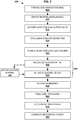
- FIG. 5 a flowchart illustrates a process flow for a method 500 of forming an integrated circuit that includes one or more nanowire or nanoribbon transistor, in accordance with an embodiment of the present disclosure.
- Processes in method 500 include blanket deposition techniques and/or any other suitable techniques as will be apparent in light of this disclosure.
- processes in this example are described in the context of forming a nanowire FinFET transistor, other nanowire or nanoribbon structures can be formed using a variation of method 500, including planar transistor configurations, vertical transistor structures, TFETs, and the like.
- method 500 begins with providing 505 a semiconductor substrate 110.
- the substrate 110 may include any suitable material, such as monocrystalline semiconductor material that includes at least one of silicon (Si), germanium (Ge), carbon (C), tin (Sn), phosphorous (P), boron (B), arsenic (As), antimony (Sb), indium (In), and gallium (Ga) to name a few examples.
- the substrate 110 is bulk silicon, such as monocrystalline silicon wafer.
- the substrate 110 can be any suitable semiconductor material, including silicon, silicon carbide (SiC), gallium nitride (GaN), and gallium arsenide (GaAs) to name a few examples.
- the substrate 110 can be selected in some embodiments from III-V materials and group IV materials.
- the substrate 110 can comprise a semiconductor material layer deposited or grown on a substrate, such as silicon carbide layer epitaxially grown on a sapphire substrate.
- the substrate 110 in some embodiments may include a Si on insulator (SOI) structure where an insulator/dielectric material (e.g., an oxide material, such as silicon dioxide) is sandwiched between two Si layers (e.g., in a buried oxide (BOX) structure), or any other suitable substrate where the top layer includes monocrystalline Si.
- SOI Si on insulator
- BOX buried oxide
- the substrate 110 may be doped with any suitable n-type and/or p-type dopant at a dopant concentration in the range of 1E16 to 1E22 atoms per cubic cm, for example.
- a silicon substrate can be p-type doped using a suitable acceptor (e.g., boron) or n-type doped using a suitable donor (e.g., phosphorous, arsenic) with a doping concentration of at least 1E16 atoms per cubic cm.
- a suitable acceptor e.g., boron
- a suitable donor e.g., phosphorous, arsenic
- the substrate 110 may be undoped/intrinsic or relatively minimally doped (such as including a dopant concentration of less than 1E16 atoms per cubic cm), for example.
- the substrate 110 is a substrate consisting essentially of Si, such as a monocrystalline silicon wafer.
- the substrate 110 may primarily include Si but may also include other material (e.g., a dopant at a given concentration). Also, note that the substrate 110 may include relatively high quality or device-quality monocrystalline Si or other material that provides a suitable template or seeding surface from which other monocrystalline semiconductor material features and layers can be formed. Therefore, unless otherwise explicitly stated, a substrate 110 as described herein is not intended to be limited to a substrate that only includes Si.
- the substrate 110 may have a crystalline orientation described by a Miller index of (100), (110), or (111), or its equivalents, as will be apparent in light of this disclosure.
- the substrate 110 in this example embodiment is shown for ease of illustration as having a thickness (dimension in the Y-axis direction) similar to that of other layers in the figures, the substrate 110 may be relatively much thicker than the other layers, such as having a thickness in the range of 1 to 950 microns (or in the sub-range of 20 to 800 microns), for example, or any other suitable thickness or range of thicknesses as will be apparent in light of this disclosure.
- the substrate 110 may include a multilayer structure including two or more distinct layers that may or may not be compositionally different.
- the substrate 110 may include grading (e.g., increasing and/or decreasing) of one or more material concentrations throughout at least a portion of the material.
- the substrate 110 may be used for one or more other IC devices, such as various diodes (e.g., light-emitting diodes (LEDs) or laser diodes), various transistors (e.g., MOSFETs or TFETs), various capacitors (e.g., MOSCAPs), various microelectromechanical systems (MEMS), various nanoelectromechanical systems (NEMS), various radio frequency (RF) devices, various sensors, or any other suitable semiconductor or IC devices, depending on the end use or target application.
- the structures described herein may be included in a system-on-chip (SoC) application, as will be apparent in light of this disclosure.
- SoC system-on-chip
- Method 500 continues with depositing 510 buffer material 112 on the substrate 110.
- the buffer material is a layer with a thickness no greater than 200 nm and has a relaxed lattice constant relative to the substrate 110.
- the substrate 110 consists essentially of monocrystalline silicon and the relaxed buffer material 112 is Si 1-x Ge x with x from 0.2 to 0.45.
- the buffer material is SiGe with a germanium content of 20-25 at%, 20-30 at%, 25-30 at%, 30-35 at%, 30-40 at%, 35-40 at%, 35-45 at%, or 40-45 at%.
- the buffer material 112 has a thickness of 300 nm or less, 250 nm or less, 200 nm or less, 150 nm or less, 100 nm or less, 50 nm or less, or 20 nm or less.
- the buffer material 112 is optionally annealed.
- the buffer material 112 optionally can be polished to planarize the material and/or to reduce the material to the desired thickness, as will be appreciated.
- depositing 510 the buffer material 112 includes a depositing a multilayer stack on the layer of buffer material 112, where the multilayer stack has up to 100% Ge and is capable of further relaxation to facilitate strained and nominally defect-free SiGe channel layers with up to 85% Ge.
- the buffer includes a layer of a first buffer material on the base and one or more additional layers of compositionally different material.
- the first layer of buffer material is Si 1-x Ge x with x from 0.2 to 0.45, such as about 0.3. Successive SiGe layers can be deposited on the first layer of buffer material to further relax the in-plane lattice constant in a way that maintains a nominally defect-free condition.
- the multilayer stack includes successive layer pairs of Si and SiGe.
- the additional buffer layers can be a plurality of layers of SiGe with successively increasing germanium content up to 85%.
- the additional buffer materials include a plurality of layers of SiGe, where each layer of SiGe has a lattice mismatch of about two percent or less with the layer of SiGe below it. Structures formed according to methodologies of the present disclosure can provide channel materials that are virtually free of stacking faults, resulting in improved carrier mobility over channel material formed according to traditional methods.
- Method 500 continues with depositing 515 a layer stack 134 on the relaxed buffer material 112, where the layer stack 134 has alternating layers of a sacrificial material 136 and channel material 138, in accordance with some embodiments.
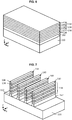
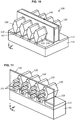
- FIG. 6 illustrates a perspective view of an example structure with a silicon substrate 110, a layer of relaxed buffer material 112 (SiGe), and a layer stack 134 of sacrificial material 136 and channel material 138.
- alternating blanket layers of sacrificial material 136 and channel material 138 can be formed using layer-by-layer epitaxial growth, where the sacrificial material 136 can subsequently be removed to release nanowires of the channel material 138.
- a first layer of sacrificial material 136 is formed directly on the relaxed buffer material 112, followed by forming a first layer of channel material 138 directly on the first layer of sacrificial material 136, and followed similar fashion by depositing additional layer pairs of sacrificial material 136 and channel material 138, and finally followed by depositing a top layer of sacrificial material 136.
- the sacrificial material 136 when the first (bottom) layer and the last (top) layer of the layer stack 134 is the sacrificial material 136, layers of channel material 138 (e.g., SiGe) are sandwiched between layers of the sacrificial material 136.
- the sacrificial material 136 is monocrystalline silicon (Si)
- the channel material 138 is monocrystalline silicon germanium (SiGe).
- the sacrificial material 136 is SiGe and the channel material 138 is Si.
- Other pairs of sacrificial material 136 and channel material 138 can be used, as will be appreciated.
- the channel material optionally can be doped with a suitable dopant at a desired concentration, as will be appreciated.
- Layer stack 134 can be formed using any suitable techniques, such as one or more deposition or epitaxial growth processes (e.g., CVD, PVD, ALD, VPE, MBE, LPE), melt regrowth, and/or any other suitable processing, as will be appreciated in light of the present disclosure.
- the sacrificial material 136 and the channel material 138 are deposited as blanket layers on the relaxed buffer material 112. Additional processing can be performed after depositing each layer, if so desired, such as cleaning and polishing one material prior to deposition of the next material.
- a given material of the layer stack 134 has a vertical thickness (dimension in the Z-axis direction) in the range of 5 nm to 50 nm (or in a subrange of 5-45, 5-40, 5-35. 5-30. 5-25, 5-20, 5-15, 5-10, 10-40, 10-30, 10-20, 15-40, 15-30, 15-20, 20-40, 20-30 and 30-40 nm) and/or a maximum vertical thickness of at most 50, 40, 30, 25, 20, 15, or 10 nm, for example.
- Other vertical thickness requirements or thresholds can be used, as will be apparent in light of this disclosure.
- the vertical thickness of each layer can be selected to provide the desired geometry of the nanowire, nanoribbon, or nanosheet to be subsequently formed, as will be appreciated.
- the materials in the layer stack 134 need not have the same vertical thickness from layer to layer nor among layers of a given material.
- subsequently formed nanowires can have vertical spacing and vertical nanowire dimensions that may be the same or different for each nanowire, as will be appreciated.
- multiple different channel materials may be formed on different areas of the substrate, such as for CMOS applications, for example.
- a first channel material 138 e.g., SiGe
- a second channel material 138 e.g., Si
- the buffer material 112 By selecting the buffer material 112 to have the desired properties (e.g., lattice constant, bandgap), multiple different channel materials 138 can be formed.
- the first channel material may include a n-type group III-V or group IV material and a second channel material may include a p-type group III-V or group IV material.
- the first channel material 138 may include group IV semiconductor material (e.g., Si, SiGe, Ge, etc.) and the second channel material 138 may include group III-V semiconductor material (e.g., GaAs, InGaAs, InP, etc.).
- group IV semiconductor material e.g., Si, SiGe, Ge, etc.
- group III-V semiconductor material e.g., GaAs, InGaAs, InP, etc.
- a given channel material may include monocrystalline group IV semiconductor material and/or group III-V semiconductor material.
- the channel region may include both group IV semiconductor material (e.g., for the broader or narrower portions) and group III-V semiconductor material (e.g., for the other of the broader or narrower portions).
- the multiple different channel materials may be formed using any suitable techniques, such as masking, depositing, and removing the masking as desired to form any number of compositionally different channel materials. Numerous different channel material configurations and variations will be apparent in light of this disclosure.
- each fin 160 has a subfin portion 162 comprising the relaxed buffer material 112 (e.g., Si 1-x Ge x where 20 ⁇ x ⁇ 45), and an upper fin portion of alternating layers of sacrificial material 136 (e.g., Si) and channel material 138 (e.g., Si 1-x Ge x where 30 ⁇ x ⁇ 85).
- the Ge concentration in the channel material 138 is greater than the Ge concentration in the relaxed buffer material 112.
- the relaxed buffer material 112 has 40 at% Ge and the channel material 138 has 50 at% Ge or more (i.e., at difference of 10 at% or more).
- regions to be processed 520 into fins are masked, followed by etching the surrounding regions to define one or more fins.
- the anisotropic etch proceeds substantially vertically through the layer stack 134 to define isolation trenches between adjacent fins 160.
- the etch process proceeds into the substrate 110 to define a fin that includes a subfin portion comprising the relaxed buffer material 112 and substrate material.
- the etch process defines groups of parallel fins 160 extending vertically up from the substrate 110.
- FIG. 7 illustrates a perspective view of one example structure showing fins 160 extending up from the substrate 110.
- Each fin 160 includes a subfin portion 162 that includes the relaxed buffer material 112 and, in some cases, also includes some substrate material.
- Each fin 160 has alternating layers of sacrificial material 136 and channel material 138 from the layer stack 134.
- the etch defines planar or 3D transistor structures having an H shape, where the channel region 130 corresponds to the horizontal beam of the H extending between the source and drain regions 120 represented by a rectangular shape connected by the channel region 130 extending therebetween.
- fins 160 are defined by forming the alternating layers of sacrificial material 136 and channel material 138 on the substrate 110 or relaxed buffer material 112 by growth or deposition in a trench.
- method 500 includes a replacement fin-based approach, in accordance with some embodiments.
- the trench is an aspect ratio trapping trench ("ART" trench) defined in a layer of insulating material, such as silicon dioxide (SiO2) formed by thermal oxidation or by deposition using a suitable one of the aforementioned techniques. The insulating material is then patterned and etched to define trenches that extend to a substrate or other material layer.
- ART aspect ratio trapping trench
- a relaxed buffer material 112 can be formed directly on the substrate 110 in the lower portion of the trench, followed by alternating layers of the sacrificial material 136 and channel material 138.
- the insulating material can then be recessed to expose all or part of the fin 160.
- the insulating material is recessed to the top of the subfin (i.e., buffer material 112) to expose only the layer stack 134 of sacrificial material 136 and channel material 138 in the upper portion of the fin 160.
- the insulating material is recessed completely to expose the entire subfin 162 of relaxed buffer material 112 and substrate material, or recessed to a level below the first layer of sacrificial material 136 to expose a portion of the subfin 162. Numerous variations and embodiments will be apparent in light of the present disclosure.
- defining 520 fins may be performed using a replacement fin-based approach.
- the replacement fin-based approach includes forming fins in the substrate, such as by patterning and etching bulk semiconductor material. Shallow trench isolation (STI) material is the formed around those fins, followed by recessing the native-to-substrate fins to define fin-shaped trenches in the STI material. The relaxed buffer material 112 and alternating layers of sacrificial material 136 and channel material 138 can then be formed in the fin-shaped trenches.
- the replacement fin approach continues with removing the STI material and forming an insulating material on the substrate 110 between the subfins 162, leaving the layer stack 134 of alternating sacrificial material 136 and channel material 138 exposed.
- the subfin is a Group IV semiconductor material, such as single-crystal Si, Ge, or SiGe.
- the subfin material is a Group III-V semiconductor material, such as GaAs, InGaAs, AlGaAs, or AlAs, to name a few examples.
- the subfin material may or may not be doped with a suitable dopant (e.g., boron, phosphorous, and/or arsenic).
- the subfin material may be n-type doped (e.g., with phosphorous or arsenic) or p-type doped (e.g., with boron) at a dopant concentration in the range of 1E16 to 1E22 atoms per cubic cm, for example.
- the subfins may have a multilayer structure including two or more distinct layers (that may or may not be compositionally different).
- the subfins may include grading (e.g., increasing and/or decreasing) of one or more material concentrations throughout at least a portion of the sub fin material.
- each fin may include a vertical fin height (dimension in the Y-axis direction) in the range of 20-500 nm (or in a subrange of 20-50, 20-100, 20-200, 20-300, 20-400,50-100, 50-200, 50-300, 50-400, 50-500, 100-250, 100-400, 100-500, 200-400, or 200-500 nm) and/or a maximum vertical fin height of at most 500, 450, 400, 350, 300, 250, 200, 150, 100, or 50 nm, for example.
- each fin may include a horizontal fin width (dimension in the X-axis direction) in the range of 2-50 nm (or in a subrange of 2-5, 2-10, 5-10, 5-20, 5-30, 5-50, 10-20, 10-30, 10-50, 20-30, 20-50, or 30-50 nm) and/or a maximum horizontal fin width of at most 50, 30, 20, 10, or 5 nm, for example.
- the ratio of fin height to fin width may be greater than 1, such as greater than 1.5, 2, 2.5, 3, 3.5, 4, 4.5, 5, 6, 7, 8, 9, 10, 15, 20, or greater than any other suitable threshold ratio, as will be apparent in light of this disclosure. Other suitable materials and thickness values/ranges/thresholds will be apparent in light of this disclosure.
- the substrate 110 or relaxed buffer material 112 may be oppositely type doped relative to the overlying channel material 138 to provide a tunnel diode configuration to help reduce or eliminate parasitic leakage (e.g., subthreshold leakage).
- the relaxed buffer material 112 may be intentionally p-type doped (e.g., with a doping concentration of at least 1E16, 5E16, 1E17, 5E17, 1E18, 5E18, or 1E19 atoms per cubic cm) if the overlying material is to be n-type doped, or vice versa.
- Method 500 continues with defining 525 a gate structure 140 in contact with the top and sides of each fin 160.
- process 525 includes filling trenches between the fins 160 with shallow trench isolation (STI) material 152.
- STI shallow trench isolation
- Such processing can include depositing the STI material 152 and then optionally planarizing/polishing the structure (e.g., via CMP).
- deposition of the STI material 152 may include any suitable deposition techniques, such as those described herein (e.g., CVD, ALD, PVD), or any other suitable deposition process.
- STI material 152 may include any suitable electrical insulator material, such as one or more dielectric, oxide (e.g., silicon dioxide), and/or nitride (e.g., silicon nitride) materials.
- the STI material 152 may be selected based on the material of the substrate 110.
- the STI material 152 may be selected from silicon dioxide or silicon nitride based on the use of a Si substrate 110.
- the STI material 152 is recessed to expose the layer stack 134 portion of the fins 160.
- the gate structure 140 is a dummy gate structure formed on the channel region 130 of the fins 160.
- the gate structure 140 includes a dummy gate oxide 144, a dummy gate electrode 142 (e.g., polysilicon), and optionally, a hardmask 148.
- defining 525 the gate structure 140 is performed in accordance with a gate-last process flow.
- the dummy gate electrode 142 is made of polysilicon or other suitable material, as will be appreciated.
- a gate-last fabrication process may utilize a dummy gate structure 140 to allow for replacement gate processing, while a gate-first fabrication process may form the final gate structure in the first instance; the final gate structure can be formed after the S/D regions 120 have been processed.
- the techniques may be performed using a gate-first process flow.
- the end structure will include the final gate stack, as will be apparent in light of this disclosure.
- the dummy gate structure can define the channel region 130 and source/drain (S/D) regions 120 of each fin 160, where the channel region 130 is below the gate structure 140 (whether dummy or final gate stack), and the source and drain regions 120 are on either side of the gate structure 140 and connect to the channel region 130.
- Process 525 includes forming gate spacers 146 on opposite sides of the dummy gate stack, which includes the gate electrode 142 and gate dielectric 144.
- the gate spacers 146 may include any suitable material, such as any suitable electrical insulator, dielectric, oxide (e.g., silicon oxide), and/or nitride (e.g., silicon nitride) material, as will be apparent in light of this disclosure.
- Gate spacers are formed along opposite sides of the dummy gate electrode.
- the gate spacers 146 are formed of silicon nitride (Si 3 N 4 ).
- a hardmask 148 may be formed over the dummy gate structure 140 to protect the dummy gate electrode 142 and gate spacers 146 during subsequent processing, for example.
- the hardmask 148 is formed on top of the dummy gate stack between the gate spacers 146.
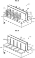
- FIG. 8 illustrates a perspective view of an example structure with fins 160 extending up from substrate 110 and STI material 150 between the subfin portion 162 of the fins 160.
- the dummy gate structure 140 is formed in contact with the top and sides of each fin 160, defining the channel region 130 below it.
- the gate structure 140 includes a dummy gate electrode 142, gate spacers 146 on opposite lateral sides of the gate electrode 142, and a hardmask 148 on top of the dummy gate electrode 142.
- Method 500 continues with processing 545 the source/drain regions 120 using any suitable techniques, in accordance with an embodiment of the present disclosure.
- processing 545 the source and drain regions 120 can be performed by etching 530 at least a portion of the exposed source and drain portion 120 of the fins 160.
- the source and drain regions 120 of the fins 160 are recessed by etching.
- all of the layer stack 134 is removed in the source and drain regions 120 of the fin, in addition to a small amount of the relaxed buffer material 112 below the layer stack 134.
- the etch process stops short of completely removing the layer stack 134 at the source and drain regions 120, leaving behind a stub or residual portion of the fins 160.
- the stub is a portion of the first (bottom) layer of sacrificial material 136 (e.g., Si) formed on the layer of relaxed buffer material 112 (e.g., SiGe).
- the source/drain etch exposes ends of the nanowire/nanoribbon channel material 138 at the outside surface of the gate spacers 146.
- the resulting structure may be masked as needed for deposition or growth of replacement source/drain material, as discussed in more detail below.
- the exposed layer stack 134 in the source/drain regions of the fins need not be completely removed; instead, the material in the layer stack 134 at the source/drain regions 120 is converted to final source/drain regions by doping, implantation, and/or cladding with a source/drain material or other suitable processing, for example.
- FIG. 9 illustrates a perspective view of an example structure after recessing the layer stack 134 in the source and drain regions 120.
- the layer stack 134 in the S/D regions 120 has been recessed to the subfin portion 162 of relaxed buffer material 112.
- the S/D regions can be further recessed, such as to the top surface of the substrate 110 or into the substrate 110.
- the channel material 138 in the channel region 130 is exposed at the face of the gate spacer 146.
- process 545 includes depositing 540 a layer of isolation material 150 over the etch S/D regions 120.
- a blanket layer of isolation material 150 is deposited conformally on the structure of FIG. 9 .
- the isolation material 150 can be an oxide (e.g., SiO2), nitride (e.g., Si 3 N 4 ), a low-k dielectric (e.g., porous SiO 2 or material having a dielectric constant below 3.9), alumina, oxynitride compounds, carbonoxynitride compounds, a spin-on C-rich glass, or some other electrically insulating material.
- the isolation material 150 is useful to inhibit source-to-drain parasitic leakage via the relaxed buffer and/or substrate 110.
- FIG. 10 illustrates a perspective view of an example structure showing the layer of isolation material 150.
- An etch-resistant material can then be deposited conformally over the isolation material 150, followed by etching. Such processing leaves a layer of isolation material 150 on the subfin 162 portions of the fins 160, where the isolation material 150 blocks epitaxial growth from the subfin 162.
- Process 545 continues with epitaxially growing 535 replacement material in the source and drain region 120 using any suitable techniques, such as vapor-phase epitaxy (VPE), molecular beam epitaxy (MBE), or liquid-phase epitaxy (LPE), for example.
- VPE vapor-phase epitaxy
- MBE molecular beam epitaxy
- LPE liquid-phase epitaxy
- Material of the source and drain regions 120 can be epitaxially grown laterally from the channel material 138 exposed at the gate spacer 146.
- single-crystal material grows hemispherically outward from the exposed ends of the channel material 138.
- growing 535 the material of the S/D regions includes growth of a Ge-rich end portion 124 originating from the exposed channel material 138.
- the channel material is SiGe
- the end portion 124 can have up to 100% Ge.
- the end portion 124 gradually decreases in Ge concentration along the end portion 124 moving away from the channel material 138.
- the end portion 124 has a graded Ge concentration from 100% where the S/D contacts the channel material 138, and gradually reduces to about 80% Ge at the body portion 122 of the S/D region 120.
- the end portion 124 has two or more distinct layers of SiGe with reducing concentration of Ge in each layer moving from a layer in contact with the channel region 130 to a layer in contact with the S/D body portion 122.
- the end portion 122 of the S/D region 120 includes carbon (e.g., up to 4%, including 1-2%) or tin (up to 10%).
- growing 535 the material of the S/D region 120 begins with growing the end portion 124 of SiGeC or SiGeSn, where the end portion has at least 80% Ge and includes carbon or tin; the balance is Si plus any dopants or other impurities, as will be appreciated.
- the end portion 124 has up to 4% C or Sn and the Ge content of at least 50 at%.
- the material of the S/D region(s) can change in concentration of Ge from a Ge-rich end portion adjacent the channel region 130 to a Si-rich region further away from the channel region 130.
- the end portion 124 of the S/D region 120 has a lateral thickness no greater than 10 nm (e.g., measured between the S/D body portion 122 and the channel region 130). In some embodiments, the end portion 124 has a lateral thickness of 2 nm or less, 4 nm or less, 6 nm or less, 8 nm or less, 10 nm or less, 15 nm or less, or 20 nm or less. Other suitable values of thickness for the end portion 124 will be apparent in light of the present disclosure.
- the source and drain regions 120 may be formed one polarity at a time, such as processing one of n-type and p-type regions, and then processing the other of the n-type and p-type regions.
- the source and drain regions 120 may include any suitable doping scheme, such as including suitable n-type and/or p-type dopant (e.g., in a concentration in the range of 1E16 to 1E22 atoms per cubic cm).
- at least one source or drain region 120 may be undoped/intrinsic or relatively minimally doped, such as including a dopant concentration of less than 1E16 atoms per cubic cm, for example.
- one or more of the S/D regions may have a multilayer structure including two or more distinct layers, for example.
- one or more of the layers of the S/D regions 120 may include grading (e.g., increasing and/or decreasing) the content/concentration of one or more materials in some or all of the region(s). For instance, in some embodiments, it may be desired to gradually increase the concentration of a given dopant or element (e.g., Ge) as a given S/D region 120 is formed.
- the S/D region has a relatively lower doping concentration near the channel region 130 and a relatively higher doping concentration near the corresponding S/D contact for improved contact resistance.
- a dummy electrode can be formed in the S/D regions 120. Such dummy electrode can be subsequently removed for further processing as discussed below.
- FIG. 10 illustrates a perspective view of an example structure after epitaxial growth of the replacement material in the S/D regions 120.
- a layer of isolation material 152 is below the S/D region 120 and contacts the top of the subfin 162.
- Process 550 may begin with removing the dummy gate electrode 142 between the gate spacers 146 to expose the channel region 130 of each fin 160.
- a dummy gate electrode 142 of polycrystalline silicon can be removed using a wet etch process (e.g., nitric acid/hydrofluoric acid), an anisotropic dry etch, or other suitable etch process, as will be appreciated.
- a wet etch process e.g., nitric acid/hydrofluoric acid
- an anisotropic dry etch e.g., nitric acid/hydrofluoric acid
- the layer stack 134 of alternating layers of channel material 138 and sacrificial material 136 is exposed in the channel region 130.
- the channel region 130 of the layer stack 134 extends between and contacts the source and drain regions 120, where ends of the layer stack 134 are protected by the gate spacers 146.
- the sacrificial material 136 can be removed by etch processing, in accordance with some embodiments. For example, an etch process that is selective to remove the sacrificial material (e.g., Si) in the layer stack is used to release 550 nanowires 132 of the channel material (e.g., SiGe).
- Etching the sacrificial material 136 may be performed using any suitable wet or dry etching process such that the etch process selectively removes the sacrificial material 136 and leaves intact the channel material 138.
- the sacrificial material 136 is silicon germanium (SiGe) and the channel material 138 is electronic grade silicon (Si), such as for an n-channel device.
- SiGe silicon germanium
- Si electronic grade silicon
- a gas-phase etch using an oxidizer and hydrofluoric acid (HF) has shown to selectively etch SiGe in SiGe/Si layer stacks.
- a gas-phase chlorine trifluoride (ClF 3 ) etch is used to remove the sacrificial SiGe material.
- silicon can be etched selectively over SiGe using a H 2 /CF 4 /Ar plasma, such as for a p-channel device, as will be appreciated.
- the etch chemistry can be selected based on the germanium concentration, nanowire dimensions, and other factors, as will be appreciated.
- the resulting channel region 130 includes nanowires 132 extending between the epitaxial material of the source and drain regions 120, where ends of the nanowires 132 (e.g., SiGe) contact the source and drain regions 120 and remain at least partially protected by the gate spacers 146.
- the released nanowires 132 or nanoribbons can be cleaned and/or shaped using a series of oxide formation and etchback, as will be appreciated.
- a thin surface oxide can be formed using thermal oxidation, deposition of an oxide plus annealing, or other suitable process.
- a wet or dry etch process can then be used to remove the oxide.
- Such a sequence of oxidation and oxide removal can remove residual amounts of the sacrificial material 136 and other impurities on the channel material 138.
- FIG. 11 shows a part of the structure of FIG. 10 after releasing nanowires 132 of the channel material 138. Ends of the channel material 138 contacting the S/D region 120
- the dummy electrode is removed, followed by performing a dimple etch to remove the sacrificial material 136 under the gate spacer 146.
- the dummy electrode is an amorphous material (e.g., polysilicon) that is removed using a suitable wet or dry etch process.
- the opening left by the dimple etch can be filled with a low-k dielectric material. In doing so, when depositing high-k dielectric during gate processing, the high-k dielectric is present only under the gate electrode 142, rather than extending into the cavity between ends of the nanowires protected by the gate spacer 146.
- Gate processing 560 includes deposition of a gate dielectric 144 on the released nanowires/nanoribbons 132, followed by deposition of a gate electrode 142 over the gate dielectric 144, in accordance with some embodiments.
- the gate stack is formed using a gate-last fabrication flow, which may be considered a replacement gate or replacement metal gate (RMG) process.
- RMG replacement gate or replacement metal gate
- the gate stack substantially (or completely) surrounds each nanowire body portion, such as wrapping around at least 80, 85, 90, 95% or more of each nanowire body.
- Gate processing 560 includes depositing a gate dielectric 144 on the exposed nanowire bodies in the channel region 130, followed by formation of a gate electrode 142 in contact with the gate dielectric 144.
- FIG. 12 illustrates a perspective view of a transistor structure 100 after gate processing 560, in accordance with some embodiments. Any suitable technique can be used, including spin-coating or CVD deposition, for example.
- the gate dielectric 144 may include, for example, any suitable oxide (such as silicon dioxide), high-k dielectric material, and/or any other suitable material as will be apparent in light of this disclosure.
- high-k dielectric materials include, for instance, hafnium oxide, hafnium silicon oxide, lanthanum oxide, lanthanum aluminum oxide, zirconium oxide, zirconium silicon oxide, tantalum oxide, titanium oxide, barium strontium titanium oxide, barium titanium oxide, strontium titanium oxide, yttrium oxide, aluminum oxide, lead scandium tantalum oxide, and lead zinc niobate, to provide some examples.
- the gate dielectric 144 can be annealed to improve its quality when high-k dielectric material is used.
- the gate electrode 142 may include a wide range of materials, such as polysilicon or various suitable metals or metal alloys, such as aluminum (Al), tungsten (W), titanium (Ti), tantalum (Ta), copper (Cu), titanium nitride (TiN), or tantalum nitride (TaN), for example.
- the gate dielectric 144 and/or gate electrode 142 may include a multilayer structure of two or more material layers, for example.
- a multilayer gate dielectric 144 may be employed to provide a more gradual electric transition from the channel region to the gate electrode, for example.
- the gate dielectric and/or gate electrode may include grading (e.g., increasing and/or decreasing) the content or concentration of one or more materials in at least a portion of the feature(s).
- one or more additional layers may also be present in the final gate stack, such as one or more relatively high or low work function layers and/or other suitable layers.
- the gate dielectric 144 may also be used to form replacement gate spacers on one or both sides of the nanowire body, such that the gate dielectric 144 is between the gate electrode 142 and one or both gate spacers 146, for example. Numerous different gate stack configurations will be apparent in light of this disclosure.
- Method 500 continues with forming 570 source/drain contacts 126.
- process 570 includes first removing the dummy electrodes formed on the source/drain regions 120.
- the source and drain contacts 126 can be formed 570 using any suitable techniques, such as forming contact trenches in an ILD layer deposited over the respective source/drain regions, followed by depositing metal or metal alloy (or other suitable electrically conductive material) in the contact trenches.
- forming 570 source/drain contacts 126 may include silicidation, germanidation, III-V-idation, and/or annealing processes, for example.
- the source and drain contacts may include aluminum or tungsten, although any suitable conductive metal or alloy can be used, such as silver, nickel-platinum, or nickel-aluminum, for example.
- one or more of the source and drain contacts may include a resistance reducing metal and a contact plug metal, or just a contact plug, for instance.
- Example contact resistance reducing metals include, for instance, nickel, aluminum, titanium, gold, gold-germanium, nickel-platinum, nickel aluminum, and/or other such resistance reducing metals or alloys.
- Example contact plug metals include, for instance, aluminum, copper, nickel, platinum, titanium, or tungsten, or alloys thereof, although any suitably conductive contact metal or alloy may be used.
- additional layers may be present in the source and drain contact regions, such as adhesion layers (e.g., titanium nitride) and/or liner or barrier layers (e.g., tantalum nitride), if so desired.
- a contact resistance reducing layer may be present between a given source or drain region and its corresponding source or drain contact 126, such as a relatively highly doped (e.g., with dopant concentrations greater than 1E18, 1E19, 1E20, 1E21, or 1E22 atoms per cubic cm) intervening semiconductor material layer, for example.
- the contact resistance reducing layer may include semiconductor material and/or impurity dopants based on the included material and/or dopant concentration of the corresponding source or drain region 120, for example.
- FIG. 14 illustrates a perspective view of a transistor structure 100 with S/D contacts 126 formed on S/D regions 120, in accordance with some embodiments.
- FIG. 13 illustrates a perspective view of a transistor structure 100 with S/D contacts 126 on S/D regions 120.
- Method 500 continues with completing 580 a general integrated circuit (IC) as desired, in accordance with some embodiments.
- IC general integrated circuit
- Such additional processing to complete an IC may include back-end or back-end-of-line (BEOL) processing to form one or more metallization layers and/or interconnect in contact with the transistor devices formed, for example. Any other suitable processing may be performed, as will be apparent in light of this disclosure.
- BEOL back-end or back-end-of-line
- Any other suitable processing may be performed, as will be apparent in light of this disclosure.
- the processes in method 500 are shown in a particular order for ease of description. However, one or more of the processes may be performed in a different order or may not be performed at all (and thus be optional), in accordance with some embodiments. Numerous variations on method 500 and the techniques described herein will be apparent in light of this disclosure.
- FIG. 14 illustrates a computing system 1000 implemented with integrated circuit structures and/or transistor devices formed using the techniques disclosed herein, in accordance with some embodiments of the present disclosure.
- the computing system 1000 houses a motherboard 1002.
- the motherboard 1002 may include a number of components, including, but not limited to, a processor 1004 and at least one communication chip 1006, each of which can be physically and electrically coupled to the motherboard 1002, or otherwise integrated therein.
- the motherboard 1002 may be, for example, any printed circuit board, whether a main board, a daughterboard mounted on a main board, or the only board of system 1000.
- computing system 1000 may include one or more other components that may or may not be physically and electrically coupled to the motherboard 1002.
- these other components may include, but are not limited to, volatile memory (e.g., DRAM), non-volatile memory (e.g., ROM), a graphics processor, a digital signal processor, a crypto processor, a chipset, an antenna, a display, a touchscreen display, a touchscreen controller, a battery, an audio codec, a video codec, a power amplifier, a global positioning system (GPS) device, a compass, an accelerometer, a gyroscope, a speaker, a camera, and a mass storage device (such as hard disk drive, compact disk (CD), digital versatile disk (DVD), and so forth).
- volatile memory e.g., DRAM
- non-volatile memory e.g., ROM
- graphics processor e.g., a digital signal processor
- crypto processor e.g., a graphics processor
- any of the components included in computing system 1000 may include one or more integrated circuit structures or devices formed using the disclosed techniques in accordance with an example embodiment.
- multiple functions can be integrated into one or more chips (e.g., for instance, note that the communication chip 1006 can be part of or otherwise integrated into the processor 1004).
- the communication chip 1006 enables wireless communications for the transfer of data to and from the computing system 1000.
- wireless and its derivatives may be used to describe circuits, devices, systems, methods, techniques, communications channels, etc., that may communicate data through the use of modulated electromagnetic radiation through a non-solid medium. The term does not imply that the associated devices do not contain any wires, although in some embodiments they might not.
- the communication chip 1006 may implement any of a number of wireless standards or protocols, including, but not limited to, Wi-Fi (IEEE 802.11 family), WiMAX (IEEE 802.16 family), IEEE 802.20, long term evolution (LTE), Ev-DO, HSPA+, HSDPA+, HSUPA+, EDGE, GSM, GPRS, CDMA, TDMA, DECT, Bluetooth, derivatives thereof, as well as any other wireless protocols that are designated as 3G, 4G, 5G, and beyond.
- the computing system 1000 may include a plurality of communication chips 1006.
- a first communication chip 1006 may be dedicated to shorter range wireless communications such as Wi-Fi and Bluetooth and a second communication chip 1006 may be dedicated to longer range wireless communications such as GPS, EDGE, GPRS, CDMA, WiMAX, LTE, Ev-DO, and others.
- the processor 1004 of the computing system 1000 includes an integrated circuit die packaged within the processor 1004.
- the integrated circuit die of the processor includes onboard circuitry that is implemented with one or more integrated circuit structures or devices formed using the disclosed techniques, as variously described herein.
- the term "processor" may refer to any device or portion of a device that processes, for instance, electronic data from registers and/or memory to transform that electronic data into other electronic data that may be stored in registers and/or memory.
- the communication chip 1006 also may include an integrated circuit die packaged within the communication chip 1006.
- the integrated circuit die of the communication chip includes one or more integrated circuit structures or devices formed using the disclosed techniques as variously described herein.
- multi-standard wireless capability may be integrated directly into the processor 1004 (e.g., where functionality of any chips 1006 is integrated into processor 1004, rather than having separate communication chips).
- processor 1004 may be a chip set having such wireless capability.
- any number of processor 1004 and/or communication chips 1006 can be used.
- any one chip or chip set can have multiple functions integrated therein.
- the computing system 1000 may be a laptop, a netbook, a notebook, a smartphone, a tablet, a personal digital assistant (PDA), an ultra-mobile PC, a mobile phone, a desktop computer, a server, a printer, a scanner, a monitor, a set-top box, an entertainment control unit, a digital camera, a portable music player, a digital video recorder, or any other electronic device or system that processes data or employs one or more integrated circuit structures or devices formed using the disclosed techniques, as variously described herein.
- PDA personal digital assistant
- an ultra-mobile PC a mobile phone
- desktop computer a server
- printer a printer
- a scanner a monitor
- a set-top box a set-top box
- an entertainment control unit a digital camera
- portable music player a digital video recorder
Landscapes
- Insulated Gate Type Field-Effect Transistor (AREA)
- Metal-Oxide And Bipolar Metal-Oxide Semiconductor Integrated Circuits (AREA)
Applications Claiming Priority (1)
| Application Number | Priority Date | Filing Date | Title |
|---|---|---|---|
| US16/131,520 US11450739B2 (en) | 2018-09-14 | 2018-09-14 | Germanium-rich nanowire transistor with relaxed buffer layer |
Publications (2)
| Publication Number | Publication Date |
|---|---|
| EP3624200A1 true EP3624200A1 (de) | 2020-03-18 |
| EP3624200B1 EP3624200B1 (de) | 2026-05-06 |
Family
ID=67139615
Family Applications (1)
| Application Number | Title | Priority Date | Filing Date |
|---|---|---|---|
| EP19183091.8A Active EP3624200B1 (de) | 2018-09-14 | 2019-06-28 | Germaniumreicher nanodrahttransistor mit entspannter pufferschicht |
Country Status (2)
| Country | Link |
|---|---|
| US (1) | US11450739B2 (de) |
| EP (1) | EP3624200B1 (de) |
Cited By (7)
| Publication number | Priority date | Publication date | Assignee | Title |
|---|---|---|---|---|
| EP4020589A1 (de) * | 2020-12-22 | 2022-06-29 | INTEL Corporation | Gate-all-around-integrierte schaltungsstrukturen mit germanium-diffundierten nanobandkanalstrukturen |
| WO2022177683A1 (en) * | 2021-02-19 | 2022-08-25 | Qualcomm Incorporated | P-type field effect transistor (pfet) on a silicon germanium (ge) buffer layer to increase ge in the pfet source and drain to increase compression of the pfet channel and method of fabrication |
| EP4156281A1 (de) * | 2021-09-24 | 2023-03-29 | Intel Corporation | Siliziumreiche deckschicht mit germanium- und borimplantaten für thermische stabilität und niedrigen pmos-kontaktwiderstand |
| EP4203071A1 (de) * | 2021-12-23 | 2023-06-28 | INTEL Corporation | Spannungskompensation durch ionenimplantation in einer relaxierten pufferschicht zur verhinderung von waferkrümmung |
| US12575170B2 (en) | 2021-09-23 | 2026-03-10 | Intel Corporation | Low temperature, high germanium, high boron SiGe:B pEPI with a silicon rich capping layer for ultra-low PMOS contact resistivity and thermal stability |
| US12598777B2 (en) | 2021-12-21 | 2026-04-07 | Intel Corporation | Low temperature, high germanium, high boron SiGe:B pEPI with titanium silicide contacts for ultra-low PMOS contact resistivity and thermal stability |
| EP4701363A3 (de) * | 2021-12-21 | 2026-04-08 | INTEL Corporation | Integrierte gate-all-around-schaltungsstrukturen mit source- oder drain-strukturen mit wiederaufgewachsenen zentralen teilen |
Families Citing this family (24)
| Publication number | Priority date | Publication date | Assignee | Title |
|---|---|---|---|---|
| FR3081154B1 (fr) * | 2018-05-17 | 2023-08-04 | Commissariat Energie Atomique | Procede de fabrication d'un composant electronique a multiples ilots quantiques |
| US11417729B2 (en) * | 2019-08-29 | 2022-08-16 | Taiwan Semiconductor Manufacturing Company, Ltd. | Transistors with channels formed of low-dimensional materials and method forming same |
| DE102020109756A1 (de) | 2019-08-29 | 2021-03-04 | Taiwan Semiconductor Manufacturing Co., Ltd. | Transistoren mit kanälen gebildet aus niedrigdimensionalenmaterialien und verfahren zum bilden derselben |
| US11177250B2 (en) * | 2019-09-17 | 2021-11-16 | Tokyo Electron Limited | Method for fabrication of high density logic and memory for advanced circuit architecture |
| US11289574B2 (en) * | 2019-12-26 | 2022-03-29 | Taiwan Semiconductor Manufacturing Co., Ltd. | Methods of forming epitaxial source/drain features in semiconductor devices |
| US11563015B2 (en) * | 2020-02-11 | 2023-01-24 | Taiwan Semiconductor Manufacturing Company Limited | Memory devices and methods of manufacturing thereof |
| CN111446297A (zh) * | 2020-03-31 | 2020-07-24 | 中国科学院微电子研究所 | 半导体器件及其制作方法、集成电路及电子设备 |
| US11309424B2 (en) | 2020-04-13 | 2022-04-19 | Taiwan Semiconductor Manufacturing Co., Ltd. | Semiconductor device and manufacturing method thereof |
| US12336239B2 (en) * | 2020-04-27 | 2025-06-17 | Imec Vzw | Tensile strained semiconductor monocrystalline nanostructure |
| EP3905338A1 (de) * | 2020-04-27 | 2021-11-03 | Imec VZW | Verspannte monokristalline halbleiter-nanostruktur |
| CN111799331A (zh) * | 2020-04-28 | 2020-10-20 | 中国科学院微电子研究所 | 一种半导体器件及其制作方法、集成电路及电子设备 |
| US11532702B2 (en) * | 2020-05-19 | 2022-12-20 | Taiwan Semiconductor Manufacturing Co., Ltd. | Source/drain isolation structures for leakage prevention |
| US11469326B2 (en) * | 2020-09-18 | 2022-10-11 | Taiwan Semiconductor Manufacturing Co., Ltd. | Semiconductor devices and methods of fabrication thereof |
| US11658215B2 (en) * | 2021-02-19 | 2023-05-23 | Taiwan Semiconductor Manufacturing Company, Ltd. | Method of forming contact structures |
| US11721741B2 (en) * | 2021-04-07 | 2023-08-08 | Taiwan Semiconductor Manufacturing Company Limited | Field-effect transistor and method of forming the same |
| US11688793B2 (en) * | 2021-04-08 | 2023-06-27 | Taiwan Semiconductor Manufacturing Company, Ltd. | Integrated circuit structure and manufacturing method thereof |
| KR102760156B1 (ko) | 2021-04-19 | 2025-01-23 | 삼성전자주식회사 | 반도체 장치 제조 방법 |
| CN113394295B (zh) * | 2021-06-10 | 2023-12-19 | 上海集成电路制造创新中心有限公司 | P型环栅器件堆叠结构及增强p型环栅器件沟道应力方法 |
| US11837604B2 (en) | 2021-09-22 | 2023-12-05 | International Business Machine Corporation | Forming stacked nanosheet semiconductor devices with optimal crystalline orientations around devices |
| US12191208B2 (en) | 2021-09-23 | 2025-01-07 | International Business Machines Corporation | Dual strained semiconductor substrate and patterning |
| US12575151B2 (en) | 2021-09-23 | 2026-03-10 | Intel Corporation | Gate-all-around integrated circuit structures having doped subfin |
| KR20230067393A (ko) | 2021-11-09 | 2023-05-16 | 삼성전자주식회사 | 에피택셜 웨이퍼 및 이를 이용하는 반도체 메모리 소자 |
| US20230317783A1 (en) * | 2022-03-30 | 2023-10-05 | Intel Corporation | Layered 2d semiconductors |
| CN121240436A (zh) * | 2024-06-28 | 2025-12-30 | 长鑫科技集团股份有限公司 | 半导体结构以及半导体结构的制作方法 |
Citations (3)
| Publication number | Priority date | Publication date | Assignee | Title |
|---|---|---|---|---|
| US20160104799A1 (en) * | 2014-10-10 | 2016-04-14 | Globalfoundries Inc. | Dual-strained nanowire and finfet devices with dielectric isolation |
| US20180047832A1 (en) * | 2016-08-10 | 2018-02-15 | Tokyo Electron Limited | Extension region for a semiconductor device |
| US20180151452A1 (en) * | 2016-11-29 | 2018-05-31 | Taiwan Semiconductor Manufacturing Co., Ltd. | Semiconductor device and manufacturing method thereof |
Family Cites Families (9)
| Publication number | Priority date | Publication date | Assignee | Title |
|---|---|---|---|---|
| WO2006012544A2 (en) | 2004-07-22 | 2006-02-02 | The Board Of Trustees Of The Leland Stanford Junior University | Germanium substrate-type materials and approach therefor |
| DE112011106033B4 (de) * | 2011-12-23 | 2019-03-14 | Intel Corporation | Halbleiterbauelemente mit einer aktiven Germaniumschicht mit darunterliegender Diffusionssperrschicht |
| US8729634B2 (en) | 2012-06-15 | 2014-05-20 | Taiwan Semiconductor Manufacturing Company, Ltd. | FinFET with high mobility and strain channel |
| US8847281B2 (en) | 2012-07-27 | 2014-09-30 | Intel Corporation | High mobility strained channels for fin-based transistors |
| KR102201606B1 (ko) | 2013-12-27 | 2021-01-12 | 인텔 코포레이션 | Cmos에 대한 2-축 인장 변형된 ge 채널 |
| KR102395071B1 (ko) * | 2015-05-14 | 2022-05-10 | 삼성전자주식회사 | 전계 효과 트랜지스터를 포함하는 반도체 소자 |
| US9502420B1 (en) | 2015-12-19 | 2016-11-22 | International Business Machines Corporation | Structure and method for highly strained germanium channel fins for high mobility pFINFETs |
| US11056592B2 (en) | 2017-06-30 | 2021-07-06 | Intel Corporation | Silicon substrate modification to enable formation of thin, relaxed, germanium-based layer |
| EP3729514A4 (de) * | 2017-12-20 | 2021-07-07 | INTEL Corporation | Transistor mit isolation unter quelle und senke |
-
2018
- 2018-09-14 US US16/131,520 patent/US11450739B2/en active Active
-
2019
- 2019-06-28 EP EP19183091.8A patent/EP3624200B1/de active Active
Patent Citations (3)
| Publication number | Priority date | Publication date | Assignee | Title |
|---|---|---|---|---|
| US20160104799A1 (en) * | 2014-10-10 | 2016-04-14 | Globalfoundries Inc. | Dual-strained nanowire and finfet devices with dielectric isolation |
| US20180047832A1 (en) * | 2016-08-10 | 2018-02-15 | Tokyo Electron Limited | Extension region for a semiconductor device |
| US20180151452A1 (en) * | 2016-11-29 | 2018-05-31 | Taiwan Semiconductor Manufacturing Co., Ltd. | Semiconductor device and manufacturing method thereof |
Cited By (9)
| Publication number | Priority date | Publication date | Assignee | Title |
|---|---|---|---|---|
| EP4020589A1 (de) * | 2020-12-22 | 2022-06-29 | INTEL Corporation | Gate-all-around-integrierte schaltungsstrukturen mit germanium-diffundierten nanobandkanalstrukturen |
| US12439659B2 (en) | 2020-12-22 | 2025-10-07 | Intel Corporation | Gate-all-around integrated circuit structures having germanium-diffused nanoribbon channel structures |
| WO2022177683A1 (en) * | 2021-02-19 | 2022-08-25 | Qualcomm Incorporated | P-type field effect transistor (pfet) on a silicon germanium (ge) buffer layer to increase ge in the pfet source and drain to increase compression of the pfet channel and method of fabrication |
| US12224347B2 (en) | 2021-02-19 | 2025-02-11 | Qualcomm Incorporated | P-type field effect transistor (PFET) on a silicon germanium (Ge) buffer layer to increase Ge in the PFET source and drain to increase compression of the PFET channel and method of fabrication |
| US12575170B2 (en) | 2021-09-23 | 2026-03-10 | Intel Corporation | Low temperature, high germanium, high boron SiGe:B pEPI with a silicon rich capping layer for ultra-low PMOS contact resistivity and thermal stability |
| EP4156281A1 (de) * | 2021-09-24 | 2023-03-29 | Intel Corporation | Siliziumreiche deckschicht mit germanium- und borimplantaten für thermische stabilität und niedrigen pmos-kontaktwiderstand |
| US12598777B2 (en) | 2021-12-21 | 2026-04-07 | Intel Corporation | Low temperature, high germanium, high boron SiGe:B pEPI with titanium silicide contacts for ultra-low PMOS contact resistivity and thermal stability |
| EP4701363A3 (de) * | 2021-12-21 | 2026-04-08 | INTEL Corporation | Integrierte gate-all-around-schaltungsstrukturen mit source- oder drain-strukturen mit wiederaufgewachsenen zentralen teilen |
| EP4203071A1 (de) * | 2021-12-23 | 2023-06-28 | INTEL Corporation | Spannungskompensation durch ionenimplantation in einer relaxierten pufferschicht zur verhinderung von waferkrümmung |
Also Published As
| Publication number | Publication date |
|---|---|
| US11450739B2 (en) | 2022-09-20 |
| EP3624200B1 (de) | 2026-05-06 |
| US20200091287A1 (en) | 2020-03-19 |
Similar Documents
| Publication | Publication Date | Title |
|---|---|---|
| EP3624200B1 (de) | Germaniumreicher nanodrahttransistor mit entspannter pufferschicht | |
| US11367722B2 (en) | Stacked nanowire transistor structure with different channel geometries for stress | |
| US11705518B2 (en) | Isolation schemes for gate-all-around transistor devices | |
| US11444166B2 (en) | Backside source/drain replacement for semiconductor devices with metallization on both sides | |
| US11588052B2 (en) | Sub-Fin isolation schemes for gate-all-around transistor devices | |
| US11276694B2 (en) | Transistor structure with indium phosphide channel | |
| US10886408B2 (en) | Group III-V material transistors employing nitride-based dopant diffusion barrier layer | |
| US11164974B2 (en) | Channel layer formed in an art trench | |
| US10483353B2 (en) | Transistor including tensile-strained germanium channel | |
| US12414366B2 (en) | Co-integration of high voltage (HV) and low voltage (LV) transistor structures, using channel height and spacing modulation | |
| TWI781952B (zh) | 積體電路及形成其之方法和互補金氧半導體裝置 | |
| EP4174916A1 (de) | Bildung von gate-spacern für verspannte pmos-gate-all-around-transistorstrukturen | |
| US11056592B2 (en) | Silicon substrate modification to enable formation of thin, relaxed, germanium-based layer | |
| US10749032B2 (en) | Techniques for forming transistors including group III-V material nanowires using sacrificial group IV material layers | |
| CN117597778A (zh) | 用于栅极全环绕(gaa)晶体管结构的混合沟道区 | |
| EP4191683A1 (de) | Vertiefte innere gate-abstandhalter und partieller ersatzkanal in nichtplanaren transistoren | |
| WO2019059920A1 (en) | SUBSTRATE DEFECT BLOCKING LAYERS FOR CONCEALED CHANNEL SEMICONDUCTOR DEVICES |
Legal Events
| Date | Code | Title | Description |
|---|---|---|---|
| PUAI | Public reference made under article 153(3) epc to a published international application that has entered the european phase |
Free format text: ORIGINAL CODE: 0009012 |
|
| STAA | Information on the status of an ep patent application or granted ep patent |
Free format text: STATUS: THE APPLICATION HAS BEEN PUBLISHED |
|
| AK | Designated contracting states |
Kind code of ref document: A1 Designated state(s): AL AT BE BG CH CY CZ DE DK EE ES FI FR GB GR HR HU IE IS IT LI LT LU LV MC MK MT NL NO PL PT RO RS SE SI SK SM TR |
|
| AX | Request for extension of the european patent |
Extension state: BA ME |
|
| STAA | Information on the status of an ep patent application or granted ep patent |
Free format text: STATUS: REQUEST FOR EXAMINATION WAS MADE |
|
| 17P | Request for examination filed |
Effective date: 20200918 |
|
| RBV | Designated contracting states (corrected) |
Designated state(s): AL AT BE BG CH CY CZ DE DK EE ES FI FR GB GR HR HU IE IS IT LI LT LU LV MC MK MT NL NO PL PT RO RS SE SI SK SM TR |
|
| STAA | Information on the status of an ep patent application or granted ep patent |
Free format text: STATUS: EXAMINATION IS IN PROGRESS |
|
| 17Q | First examination report despatched |
Effective date: 20211202 |
|
| REG | Reference to a national code |
Ref country code: DE Ref legal event code: R079 Free format text: PREVIOUS MAIN CLASS: H01L0029060000 Ipc: H10D0030010000 Ref country code: DE Ref legal event code: R079 Ref document number: 602019084468 Country of ref document: DE Free format text: PREVIOUS MAIN CLASS: H01L0029060000 Ipc: H10D0030010000 |
|
| GRAP | Despatch of communication of intention to grant a patent |
Free format text: ORIGINAL CODE: EPIDOSNIGR1 |
|
| STAA | Information on the status of an ep patent application or granted ep patent |
Free format text: STATUS: GRANT OF PATENT IS INTENDED |
|
| RIC1 | Information provided on ipc code assigned before grant |
Ipc: H10D 30/01 20250101AFI20251125BHEP Ipc: H10D 30/00 20250101ALI20251125BHEP Ipc: H10D 30/67 20250101ALI20251125BHEP Ipc: H10D 30/69 20250101ALI20251125BHEP Ipc: H10D 62/10 20250101ALI20251125BHEP Ipc: H10D 62/13 20250101ALI20251125BHEP Ipc: H10D 62/17 20250101ALI20251125BHEP Ipc: H10D 62/822 20250101ALI20251125BHEP Ipc: H10D 64/01 20250101ALI20251125BHEP Ipc: B82Y 10/00 20110101ALN20251125BHEP |
|
| INTG | Intention to grant announced |
Effective date: 20251209 |
|
| GRAS | Grant fee paid |
Free format text: ORIGINAL CODE: EPIDOSNIGR3 |
|
| GRAA | (expected) grant |
Free format text: ORIGINAL CODE: 0009210 |
|
| STAA | Information on the status of an ep patent application or granted ep patent |
Free format text: STATUS: THE PATENT HAS BEEN GRANTED |