EP3624441B1 - Festkörperbildaufnahmevorrichtung, ansteuerverfahren für festkörperbildaufnahmevorrichtung und elektronische vorrichtung - Google Patents
Festkörperbildaufnahmevorrichtung, ansteuerverfahren für festkörperbildaufnahmevorrichtung und elektronische vorrichtung Download PDFInfo
- Publication number
- EP3624441B1 EP3624441B1 EP18798985.0A EP18798985A EP3624441B1 EP 3624441 B1 EP3624441 B1 EP 3624441B1 EP 18798985 A EP18798985 A EP 18798985A EP 3624441 B1 EP3624441 B1 EP 3624441B1
- Authority
- EP
- European Patent Office
- Prior art keywords
- signal
- node
- period
- retaining
- sampling
- Prior art date
- Legal status (The legal status is an assumption and is not a legal conclusion. Google has not performed a legal analysis and makes no representation as to the accuracy of the status listed.)
- Active
Links
Images


Classifications
-
- H—ELECTRICITY
- H04—ELECTRIC COMMUNICATION TECHNIQUE
- H04N—PICTORIAL COMMUNICATION, e.g. TELEVISION
- H04N25/00—Circuitry of solid-state image sensors [SSIS]; Control thereof
- H04N25/70—SSIS architectures; Circuits associated therewith
- H04N25/76—Addressed sensors, e.g. MOS or CMOS sensors
- H04N25/77—Pixel circuitry, e.g. memories, A/D converters, pixel amplifiers, shared circuits or shared components
- H04N25/771—Pixel circuitry, e.g. memories, A/D converters, pixel amplifiers, shared circuits or shared components comprising storage means other than floating diffusion
-
- H—ELECTRICITY
- H04—ELECTRIC COMMUNICATION TECHNIQUE
- H04N—PICTORIAL COMMUNICATION, e.g. TELEVISION
- H04N25/00—Circuitry of solid-state image sensors [SSIS]; Control thereof
- H04N25/40—Extracting pixel data from image sensors by controlling scanning circuits, e.g. by modifying the number of pixels sampled or to be sampled
- H04N25/44—Extracting pixel data from image sensors by controlling scanning circuits, e.g. by modifying the number of pixels sampled or to be sampled by partially reading an SSIS array
- H04N25/443—Extracting pixel data from image sensors by controlling scanning circuits, e.g. by modifying the number of pixels sampled or to be sampled by partially reading an SSIS array by reading pixels from selected two-dimensional [2D] regions of the array, e.g. for windowing or digital zooming
-
- H—ELECTRICITY
- H04—ELECTRIC COMMUNICATION TECHNIQUE
- H04N—PICTORIAL COMMUNICATION, e.g. TELEVISION
- H04N25/00—Circuitry of solid-state image sensors [SSIS]; Control thereof
- H04N25/60—Noise processing, e.g. detecting, correcting, reducing or removing noise
- H04N25/616—Noise processing, e.g. detecting, correcting, reducing or removing noise involving a correlated sampling function, e.g. correlated double sampling [CDS] or triple sampling
-
- H—ELECTRICITY
- H04—ELECTRIC COMMUNICATION TECHNIQUE
- H04N—PICTORIAL COMMUNICATION, e.g. TELEVISION
- H04N25/00—Circuitry of solid-state image sensors [SSIS]; Control thereof
- H04N25/70—SSIS architectures; Circuits associated therewith
- H04N25/709—Circuitry for control of the power supply
-
- H—ELECTRICITY
- H04—ELECTRIC COMMUNICATION TECHNIQUE
- H04N—PICTORIAL COMMUNICATION, e.g. TELEVISION
- H04N25/00—Circuitry of solid-state image sensors [SSIS]; Control thereof
- H04N25/70—SSIS architectures; Circuits associated therewith
- H04N25/76—Addressed sensors, e.g. MOS or CMOS sensors
- H04N25/766—Addressed sensors, e.g. MOS or CMOS sensors comprising control or output lines used for a plurality of functions, e.g. for pixel output, driving, reset or power
-
- H—ELECTRICITY
- H04—ELECTRIC COMMUNICATION TECHNIQUE
- H04N—PICTORIAL COMMUNICATION, e.g. TELEVISION
- H04N25/00—Circuitry of solid-state image sensors [SSIS]; Control thereof
- H04N25/70—SSIS architectures; Circuits associated therewith
- H04N25/76—Addressed sensors, e.g. MOS or CMOS sensors
- H04N25/78—Readout circuits for addressed sensors, e.g. output amplifiers or A/D converters
-
- H—ELECTRICITY
- H04—ELECTRIC COMMUNICATION TECHNIQUE
- H04N—PICTORIAL COMMUNICATION, e.g. TELEVISION
- H04N25/00—Circuitry of solid-state image sensors [SSIS]; Control thereof
- H04N25/70—SSIS architectures; Circuits associated therewith
- H04N25/79—Arrangements of circuitry being divided between different or multiple substrates, chips or circuit boards, e.g. stacked image sensors
Definitions
- the present invention relates to a solid-state imaging device, a method for driving a solid-state imaging device, and an electronic apparatus.
- Solid-state imaging device including photoelectric conversion elements for detecting light and generating charges are embodied as CMOS (complementary metal oxide semiconductor) image sensors, which have been in practical use.
- CMOS image sensors have been widely applied as parts of various types of electronic apparatuses such as digital cameras, video cameras, surveillance cameras, medical endoscopes, personal computers (PCs), mobile phones and other portable terminals (mobile devices).
- the CMOS image sensor includes, for each pixel, a photodiode (a photoelectric conversion element) and a floating diffusion (FD) amplifier having a floating diffusion (FD).
- the mainstream design of the reading operation in the CMOS image sensor is a column parallel output processing of selecting one of the rows in the pixel array and reading the pixels in the selected row simultaneously in the column output direction.
- the CMOS image sensor may sequentially scan the pixels or rows one-by-one to read the charges generated by photoelectric conversion and stored in the photo-diodes.
- sequential scan in other words, a rolling shutter is employed as the electronic shutter, it is not possible to start and end the exposure for storing the charges produced by photoelectric conversion at the same time in all of the pixels. Therefore, the sequential scan has such a problem that, when a moving object is imaged, a captured image may experience distortion.
- a global shutter is employed as the electronic shutter in a case where image distortion is not acceptable, for example, for the purposes of imaging a fast-moving object and sensing that requires simultaneity among the captured images.
- the exposure can be started and ended at the same timing in all of the pixels of the pixel array part.
- JP 2009-004834 A discloses a solid-state imaging device with a pixel that includes: a photodiode for generating charges depending on the strength of an incident light; signal generating sections for generating a first voltage level in accordance with the amount of charges generated during an exposure period T1 by the photodiode and a second voltage level in accordance with the amount of charges generated during an exposure period T2 by the photodiode; signal compositing sections for compositing the first and second voltage levels generated by the signal generating sections; and a level limiting section for limiting the signal level so that the signal levels of the first and second voltage signals to be composited in the signal compositing section may not exceed a signal level equivalent the maximum accumulating quantity of the photodiode.
- an optical electronic device may include a plurality of different optical sources, and a global shutter sensor including an array of global shutter pixels, with each global shutter pixel including a plurality of storage elements.
- a controller may be coupled to the plurality of optical sources and the global shutter sensor and configured to cause a first optical source to illuminate and a first storage element in each global shutter pixel to store optical data during a first integration period, cause a second optical source to illuminate and a second storage element in each global shutter pixel to store optical data during a second integration period, and output the stored optical data from the first and second storage elements of the global shutter pixels after the first and second integration periods.
- JP 2011-078103 A discloses an imaging element with sample-hold circuits for optical signals and for noise signals are provided within a pixel, and the optical signals and the noise signals are preserved independent of exposure and are simultaneously outputted (outputted by 2 lines for each column) from the sample-hold.
- US 2012/008029 A discloses a solid-state imaging apparatus which includes a pixel array in which a plurality of pixels are arranged, wherein the pixel array has a region formed from one of an electrical conductor and a semiconductor to which a fixed electric potential is supplied, each pixel includes a photoelectric converter, a charge-voltage converter which converts charges generated by the photoelectric converter into a voltage, and an amplification unit which amplifies a signal generated by the charge-voltage converter by a positive gain and outputs the amplified signal to an output line, and the output line comprising a shielding portion arranged to shield at least part of the charge-voltage converter with respect to the region.
- US 2013/229560 A discloses a solid-state image pickup device with first and second substrates on which circuit elements constituting a pixel; a coupler electrically coupling the first and second substrates; a first photoelectric conversion element on the first substrate; a first amplifier circuit on the first substrate; a first storing unit on the second substrate; and an output circuit on the second substrate.
- the first photoelectric conversion element performs photoelectric conversion on a first incident light to generate a first signal.
- the first amplifier circuit is coupled in series to the first photoelectric conversion element.
- the first amplifier circuit amplifies the first signal to generate a first amplified signal and output the first amplified signal to the coupler.
- the first storing unit stores the first amplified signal.
- the output circuit sequentially outputs the first amplified signal stored.
- US 2015/341582 A discloses a solid-state image-capturing device which has a plurality of pixels and first and second substrates in which circuit elements constituting the pixels are arranged and which are electrically connected through a connection unit.
- the solid-state image-capturing device includes: a photoelectric conversion element included in the pixel of the first substrate; a first current source; a first amplification transistor having a source or a drain connected to the first current source and a gate to which a signal generated by the photoelectric conversion element is input; a second current source; a switch configured to switch ON and OFF of a connection between a vertical signal line and the second current source and to be turned off when the gate of the first amplification transistor is reset; a voltage output circuit configured to output a power supply voltage to the vertical signal line when the gate of the first amplification transistor is reset.
- US 2005/146617 A discloses an imaging apparatus which includes a pixel unit having a photoelectric conversion section and an amplifying device for amplifying a signal from the photoelectric conversion section and outputting the signal, a reading unit having a first mode in which a signal obtained by resetting an input section of the amplifying device is sampled a plurality of times via the amplifying device and a second mode in which a photoelectric conversion signal generated in the photoelectric conversion section is sampled a plurality of times via the amplifying device; a mixing unit for generating a first mixing signal by mixing the signals that are sampled in the first mode, outputting the first mixing signal, generating a second mixing signal by mixing the signals that are sampled in the second mode, and outputting the second mixing signal; and a difference processing unit for performing difference processing between the first mixing signal and the second mixing signal.
- JP 2015-177355 A discloses an imaging device which comprises a plurality of pixels and a control part for controlling each pixel.
- Each pixel comprises a sensor for detecting a radiation or light, a first holding part for holding a signal from the sensor, and a second holding part for holding a noise signal which may be included in the signal from the sensor.
- the control part performs control so that the first holding part holds the signal from the sensor having detected the radiation or light and the second holding part holds the noise signal in a first mode, and the first holding part holds the signal from the sensor having detected the radiation or light and the second holding part does not hold the noise signal in a second mode.
- a pixel In a CMOS image sensor employing a global shutter as the electronic shutter, a pixel has therein a signal retaining part for retaining, in a sample-and-hold capacitor, a signal that is read out from a photoelectric conversion reading part, for example.
- the CMOS image sensor employing a global shutter stores the charges from the photodiodes in the sample-and-hold capacitors of the signal retaining parts at the same time in the form of voltage signals and subsequently sequentially read the voltage signals. In this way, the simultaneity is reliably achieved among the images (see, for example, Non-patent Literature 1).
- Non-patent Literature 1 has a stacked structure in which a first substrate (a pixel die) and a second substrate (an ASIC die) are connected through micropumps (connecting parts).
- the first substrate has photoelectric conversion reading parts for individual pixels formed therein
- the second substrate has signal retaining parts for the individual pixels, signal lines, a vertical scanning circuit, a horizontal scanning circuit, a column reading circuit and the like formed therein.
- a voltage-mode global shutter is designed to perform correlated double sampling (CDS) at a location neighboring a photoelectric conversion part and thus capable of realizing high shutter efficiency (SRR) or parasitic light sensitivity (PLS) more easily than a conventional charge-mode global shutter.
- CDS correlated double sampling
- PLS parasitic light sensitivity
- the chip stacking technique enables the sampling part and the photoelectric converting part to be provided in different dies, which can accomplish complete light blocking.
- the PLS can be lowered to -160dB, which hardly affects the image obtained immediately before the entrance by sampling.
- This advantage indicates that the above-described pixel-related techniques are promising to be applied to machine-vision cameras, which requires stable images to be acquired even with extreme fluctuation in lighting such as ITS.
- sampling circuits are mounted immediately below the pixels that include photoelectric converting parts.
- a large capacitance and a switching transistor are required.
- a transistor for outputting the sampled voltage is also required.
- the sampling generates noise voltage, which is inversely proportional to the square root of the sampling capacitance. To achieve reduced noise, it is essentially necessary to implement as large a sampling capacitance as possible.
- a plurality of types of devices including a MOS capacitor, a MIM capacitor, a PIP capacitor, a MOM capacitor and a trench capacitor, are available to implement the sampling capacitance, but it is generally preferable to constitute the sampling part and the output part of the sampling circuit with as few transistors as possible.
- Non-patent Literature 3 there are two different ways to perform CDS.
- the first way uses the AC coupling technique to process the difference between the pixel reset voltage and the optical signal voltage in the sampling circuit and save the result.
- the AC coupling technique which is mentioned in the Non-patent Literature 3, can be implemented using an output part having the same configuration as in the conventional 4T-APS pixel and thus requires a reduced number of transistors. Due to the effects of the charge sharing, however, the transfer function gain of the sampling circuit may fall below 0.5 or be approximately 0.8 when different configurations are employed depending on the parasitic capacitance. This disadvantageously increases the input conversion noise very much.
- the second way uses the double sampling technique.
- the difference processing is performed in the column circuit. This necessitates an output part in each sampling capacitor as disclosed in Non-patent Literature 2 and thus tends to increase the number of transistors. Nevertheless, no charge sharing occurs, and no signal amplitude loss thus occurs in the sampling circuit.
- the pixel sensitivity can be maintained at a relatively higher level and the input conversion noise can be reduced.
- the objective of the present invention is to provide a solid-state imaging device, a method for driving a solid-state imaging device and an electronic apparatus that are capable of achieving the reduced increase in number of transistors, preventing the occurrence of signal amplitude loss in the sampling parts, maintaining high pixel sensitivity and reducing input conversion noise.
- the invention provides a solid state imaging device with the features of claim 1, an electronic apparatus according to claim 17, and a method with the features of claim 15. Further advantageous embodiments of the invention are disclosed in the dependent claims.
- the present invention can achieve the reduced increase in number of transistors, prevent the occurrence of signal amplitude loss in the sampling parts, maintain high pixel sensitivity and reduce input conversion noise.
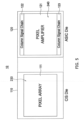
- Fig. 1 is a block diagram showing an example configuration of a solid-state imaging device according to a first embodiment of the present invention.
- the solid-state imaging device 10 is constituted by, for example, a CMOS image sensor.
- the solid-state imaging device 10 is constituted mainly by a pixel part 20 serving as an image capturing part, a vertical scanning circuit (a row scanning circuit) 30, a reading circuit (a column reading circuit) 40, a horizontal scanning circuit (a column scanning circuit) 50, and a timing control circuit 60.
- the vertical scanning circuit 30, the reading circuit 40, the horizontal scanning circuit 50, and the timing control circuit 60 constitute the reading part 70 for reading out pixel signals.
- the pixel part 20 includes pixels, and each pixel includes a photoelectric conversion reading part and a signal retaining part.
- the solid-state imaging device 10 is configured, for example, as a stacked CMOS image sensor capable of operating in a global shutter mode.
- the solid-state imaging device 10 is a stacked CMOS image sensor formed by a first substrate and a second substrate, as will be described below in detail.
- the signal retaining part formed in the second substrate is provided with a first sampling part and a second sampling part, each of which is formed by one sampling transistor (1T) and one sampling capacitor (1C).
- the coupling node between the two sampling parts serves as a retaining node and is used as a bidirectional port.
- the solid-state imaging device 10 is configured as a solid-state imaging element having a global shutter function that achieves a substantially the same signal amplitude as in the differential reading scheme with four transistors.
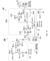
- Fig. 2 is a circuit diagram showing an example configuration of the pixel of the solid-state imaging device 10 relating to the first embodiment of the present invention.
- the pixel 21 arranged in the pixel part 20 includes a photoelectric conversion reading part 211 and a signal retaining part 212.
- a power supply switching part 22, a node potential switching part 23 and a bus resetting part 24 are arranged in correspondence with the pixel 21 or a plurality of pixels 21.
- the photoelectric conversion reading part 211 of the pixel 21 includes a photodiode (a photoelectric conversion element) and an in-pixel amplifier. More specifically, the photoelectric conversion reading part 211 includes, for example, a photodiode PD21 serving as a photoelectric conversion reading part.
- a photodiode PD21 serving as a photoelectric conversion reading part.
- the photodiode PD21 one transfer transistor TG1-Tr serving as a transferring element, one reset transistor RST1-Tr serving as a resetting element, one source follower transistor SF1-Tr serving as a first source follower element, one selection transistor SEL1-Tr serving as a selecting element and one output node ND21 are provided.
- the photoelectric conversion reading part 211 of the pixel 21 relating to the first embodiment includes four transistors (4Tr), namely, the transfer transistor TG1-Tr, the reset transistor RST1-Tr, the first source follower transistor SF1-Tr, and the selection transistor SEL1-Tr.
- the photoelectric conversion reading part 211 relating to the first embodiment has the output node ND21 connected to the input part of the signal retaining part 212 of the pixel 21.
- the photoelectric conversion reading part 211 outputs to the signal retaining part 212 a read-out signal (signal voltage) (VSIG) and a read-out reset signal (signal voltage) (VRST), as a pixel signal, in the global shutter mode.
- VSIG read-out signal
- VRST read-out reset signal
- the vertical signal line LSGN11 is driven by a constant current source Ibias in the global shutter mode.
- the photodiode PD21 generates signal charges (electrons) in an amount determined by the quantity of the incident light and stores the same. Description will be hereinafter given of a case where the signal charges are electrons and each transistor is an n-type transistor. However, it is also possible that the signal charges are holes or each transistor is a p-type transistor. Further, this embodiment is also applicable to the case where a plurality of photodiodes and transfer transistors share the transistors or the case where the pixel includes three transistors (3Tr) other than the selection transistor.
- the transfer transistor TG1-Tr of the photoelectric conversion reading part 211 is connected between the photodiode PD21 and the floating diffusion FD21 and controlled by a control signal TG applied to the gate thereof through a control line.
- the transfer transistor TG1-Tr remains selected and in the conduction state during a transfer period in which the control signal TG is at the high (H) level, to transfer to the floating diffusion FD21 the charges (electrons) produced by the photoelectric conversion and then stored in the photodiode PD21.
- the reset transistor RST1-Tr is connected between a power supply line Vdd of power supply voltage VDD and the floating diffusion FD21 and controlled by a control signal RST applied to the gate thereof through a control line.
- the reset transistor RST1-Tr remains selected and in the conduction state during a reset period in which the control signal RST is at the H level, to reset the floating diffusion FD21 to the potential of the power supply line Vdd of the power supply voltage VDD.
- the source follower transistor SF1-Tr, serving as a first source follower element, and the selection transistor SEL1-Tr are connected in series between the power supply line Vdd and the output node ND21.
- a signal line LSGN12 between the output node ND21 and the input part of the signal retaining part 212 is driven by a capacitor or constant current source, which is, for example, arranged in the signal retaining part 212.
- the gate of the source follower transistor SF1-Tr is connected to the floating diffusion FD21, and the selection transistor SEL1-Tr is controlled by the control signal SEL applied to the gate thereof through a control line.
- the selection transistor SEL1-Tr remains selected and in the conduction state during a selection period in which the control signal SEL is at the H level.
- the source follower transistor SF1-Tr outputs, through the output node ND21 to the signal line LSGN12, a read-out signal (VSIG) and a read-out reset signal (VRST) of a column output obtained by converting the charges in the floating diffusion FD21 into a voltage signal determined by the quantity of the charges (potential).
- the signal retaining part 212 of the pixel 21 basically includes an input part 2121 including the input node ND22, a first sampling part 2122, a second sampling part 2123, an output part 2124 and a retaining node ND23.
- the input node ND22 and the retaining node ND23 are directly connected.
- the first switch element of the first sampling part 2122 and the second switch element of the second sampling part 2123 are connected in parallel.
- the input part 2121 has the input node ND22 connected to the output node ND21 of the photoelectric conversion reading part 211 through the signal line LSGN12 and inputs the read-out signal (VSIG) and the read-out reset signal (VRST), which are output from the output node ND21, into the first sampling part 2122 and the second sampling part 2123 through the retaining node ND23.
- VSIG read-out signal
- VRST read-out reset signal
- the first sampling part 2122 includes a first sample-and-hold capacitor CS21 and a first sampling transistor SHS1-Tr.
- the first sample-and-hold capacitor CS21 is capable of retaining the read-out signal VSIG output from the output node ND21 of the photoelectric conversion reading part 211 and input into the input node ND22.
- the first sampling transistor SHS1-Tr serves as a first switch element that is configured to selectively connect the first sample-and-hold capacitor CS21 to the retaining node ND23.
- the first sample-and-hold capacitor CS21 is connected between the node ND24 and the reference potential VSS.
- the first sampling transistor SHS1-Tr is connected between the retaining node ND23 and the node ND24.
- the first sampling transistor SHS1-Tr is in the conduction state during a period in which, for example, the control signal SHS is at the high level.
- the first sampling transistor SHS1-Tr keeps the first sample-and-hold capacitor CS21 of the first sample holding part 2122 selectively connected to the retaining node ND23 during a global shutter period or sample-and-hold capacitor clear period.
- the second sampling part 2123 includes a second sample-and-hold capacitor CR21 and a second sampling transistor SHR1-Tr.
- the second sample-and-hold capacitor CR21 is capable of retaining the read-out reset signal VRST output from the output node ND21 of the photoelectric conversion reading part 211 and input into the input node ND22.
- the second sampling transistor SHR1-Tr serves as a second switch element that is configured to selectively connect the second sample-and-hold capacitor CR21 to the retaining node ND23.
- the second sample-and-hold capacitor CR21 is connected between the node ND25 and the reference potential VSS.
- the second sampling transistor SHR1-Tr is connected between the retaining node ND23 and the node ND25.
- the second sampling transistor SHR1-Tr is in the conduction state during a period in which, for example, the control signal SHR is at the high level.
- the second sampling transistor SHR1-Tr keeps the second sample-and-hold capacitor CR21 of the second sample holding part 2123 selectively connected to the retaining node ND23 during a global shutter period or sample-and-hold capacitor clear period.
- the reading of the signal from the photoelectric conversion reading part 211 to the signal retaining part 212 is carried out by connecting the first sample-and-hold capacitor CS21 and the second sample-and-hold capacitor CR21, which are 0V-cleared sampling capacitors, to the retaining node ND23.
- the first sampling part 2122 and the second sampling part 2123 have a one-transistor (1T) and one-capacitor (1C) configuration as in DRAM, so that charges can be bidirectionally transferred between the first and second sampling parts 2122 and 2123 and the retaining node ND23.
- both writing (sampling) and reading (charge sharing) are performed to a single point, which can achieve the reduced number of necessary transistors.
- the first sampling transistor SHS1-Tr and the second sampling transistor SHR1-Tr are formed by a MOS transistor, for example, an n-channel MOS (NMOS) transistor.
- the first sample-and-hold capacitor CS21 and the second sample-and-hold capacitor CR21 are formed by one of a MOS capacitor, a MIM capacitor, a PIP capacitor and a MOM capacitor, or a combination thereof.
- the output part 2124 includes a source follower transistor SF2-Tr serving as a second source follower element for outputting, from the source terminal thereof, the read-out signal VISG retained in the first sample-and-hold capacitor CS21 of the first sampling part 2122 and the read-out reset signal VRST retained in the second sample-and-hold capacitor CR21 of the second sampling part 2123 at a level corresponding to the voltage retained at the retaining node ND23 to the vertical signal line LSGN11.
- a source follower transistor SF2-Tr serving as a second source follower element for outputting, from the source terminal thereof, the read-out signal VISG retained in the first sample-and-hold capacitor CS21 of the first sampling part 2122 and the read-out reset signal VRST retained in the second sample-and-hold capacitor CR21 of the second sampling part 2123 at a level corresponding to the voltage retained at the retaining node ND23 to the vertical signal line LSGN11.
- the source follower transistor SF2-Tr serving as the second source follower element is connected at the source terminal thereof to the vertical signal line LSGN11, at the drain terminal thereof to the power supply switching part 22 via the power supply line Vddpix, and at the gate terminal thereof to the retaining node ND23.
- the source follower transistor SF2-Tr remains connected at the drain thereof to the power supply line Vddpix at the power supply potential VDD by the power supply switching part 22 during a retained signal reading period PHRD, in which the read-out signal VSIG and the read-out reset signal VRST retained in the first sample-and-hold capacitor CS21 and the second sample-and-hold capacitor CR21 are read out.
- the source follower transistor SF2-Tr outputs the read-out signal (VSIG) and the read-out reset signal (VRST) of a column output, which are obtained by converting the voltage retained in the retaining node ND23 into a corresponding voltage signal, to the vertical signal line LSGN11.
- the source follower transistor SF2-Tr remains connected at the drain thereof to the reference potential VSS (for example, the ground level or 0V) by the power supply switching part 22 during a clear period PCL in which the first sample-and-hold capacitor CS21 and the second sample-and-hold capacitor CR21 of the signal retaining part 212 are cleared and during a sampling period PSML in which the read-out signal and the read-out reset signal read from the photoelectric conversion reading part 211 are written into (retained in) the first sample-and-hold capacitor CS21 and the second sample-and-hold capacitor CR21.
- VSS for example, the ground level or 0V
- the output from the selecting part 221 is connected to the power supply line Vddpix connected to the drain of the source follower transistor SF2-Tr of the output part 2124 of the signal retaining part 212, and the selecting part 221 connects the power supply line Vddpix to the power supply line Vdd at the power supply potential VDD (for example, 3V) or to the reference potential VSS, according to the control signal CTL1.
- the control signal CTL1 is set to the L level during the clear period PCL or sampling period PSML, so that the selecting part 221 of the power supply switching part 22 connects the power supply line Vddpix to the reference potential VSS.
- control signal CTL1 is set to the H level during the retained signal reading period PHRD, so that the selecting part 221 of the power supply switching part 22 connects the power supply line Vddpix to the power supply line Vdd at the power supply potential VDD.
- the source terminal of the source follower transistor SF2-Tr is connected to the vertical signal line LSGN11, as described above, which is connected to the bus resetting part 24.
- the bus resetting part 24 includes a switch element 241 connected between the vertical signal line LSGN11 and the reference potential VSS. The switch element 241 is turned on or off by the bus reset signal BRST.
- the source terminal of the source follower transistor SF2-Tr serves as an impedance during the retained signal reading period PHRD as it is driven by a constant current, but is fixed at the reference potential VSS (for example, 0V) during the sampling period PSML, since the bus reset signal BRST for the switch element 241 of the bus resetting part 24 is set to turn on the switch element 241.
- VSS for example, 0V
- the source follower transistor SF2-Tr enters the strong inversion region and becomes equivalent to a MOS capacitor. This resultantly imposes band limit on the transistors preceding this MOS capacitor and can thereby reduce the noise.
- the retaining node ND23 is connected to the node potential switching part 23, which serves as a clamp circuit.
- the node potential switching part 23 is configured to be capable of selectively setting the retaining node ND23 of the signal retaining part 212 to one of a predetermined voltage level VCLP and the reference potential VSS (for example, 0V), which allows the output part 2124 of the signal retaining part 212 to realize CDS reading.
- the node potential switching part 23 serving as a clamp circuit includes a selecting part 231 and a switching transistor CLP1-Tr.
- the selecting part 231 is capable of selecting one of the predetermined voltage VCLP (for example, 2.6V) and the reference potential VSS as a clamp voltage according to the control signal CTL2, and the switching transistor CLP1-Tr is capable of selectively connecting the output line of the selecting part 231 to the retaining node ND23.
- the selecting part 231 is connected to the power supply line Vclppix connected to the source terminal of the switching transistor CLP1-Tr, and the selecting part 231 connects the power supply line Vclppix to one of the power supply line Vclp at the predetermined voltage VCLP (for example, 2.6V) and the reference potential VSS, according to the control signal CTL2.
- the control signal CTL2 is set to the L level during the clear period PCL or sampling period PSML, so that the selecting part 231 of the node potential switching part 23 connects the power supply line Vclppix to the reference potential VSS.
- control signal CTL2 is set to the H level during the retained signal reading period PHRD, so that the selecting part 231 of the node potential switching part 23 connects the power supply line Vclppix to the power supply line Vclp at the predetermined voltage VCLP.
- the switching transistor CLP1-Tr of the node potential switching part 23 is turned on or off by the control signal CLP.
- the switching transistor CLP1-Tr remains on while the control signal CLP remains at the H level, so that the retaining node is connected to the power supply line Vclppix connected to the source terminal and the retaining node ND23 is set to the predetermined voltage VCLP (for example, 2.6V) or reference potential VSS.
- the switching transistor CLP1-Tr of the node potential switching part 23 relating to the first embodiment serves as a switch element.
- the node potential switching part 23 sets the retaining node ND23 to the predetermined voltage VCLP during the retained signal reading period PHRD, so that the predetermined voltage VCLP is used as the initial voltage for the CDS reading performed by the output part 2124 of the signal retaining part 212. Furthermore, the node potential switching part 23 keeps the retaining node ND23 fixed at the reference potential VSS (for example, 0V) while reading is performed on other rows, so that the source follower transistor SF2-Tr of the output part 2124 can operate as an off switch.
- VSS for example, 0V
- the pixel signal is sampled into the signal retaining part 212 serving as a pixel signal storage, which takes place in all of the pixels at the same time, and the signals obtained by converting the read-out signals retained in the first sample-and-hold capacitor CS21 and the second sample-and-hold capacitor CR21 are read out to the vertical signal line LSGN11 and fed to the column reading circuit 40.
- the constant current source designed to drive the signal line LSGN12 between the output node ND21 of the photoelectric conversion reading part 211 and the input part of the signal retaining part 212 is not arranged in the input part 2121 of the signal retaining part 212, and the signal line LSGN12 is driven by a dynamic current source provided by the first sample-and-hold capacitor CS21 and the second sample-and-hold capacitor CR21.
- Both of the first sample-and-hold capacitor CS21 and the second sample-and-hold capacitor CR21 are cleared to and kept at 0V during the clear period, and when the first sample-and-hold capacitor CS21 and the second sample-and-hold capacitor CR21 are connected to the source follower transistor SF1-Tr of the photoelectric conversion reading part 211, the electrons are fed from the first sample-and-hold capacitor CS21 and the second sample-and-hold capacitor CR21. Accordingly, the first sample-and-hold capacitor CS21 and the second sample-and-hold capacitor CR21 serve as a dynamic current source.
- the pixels 21 each having the above-described configuration are arranged to form a pixel array, for example, as shown in Fig. 3 , and a plurality of pixel arrays are combined.
- Fig. 3 is used to illustrate the pixel arrays in the pixel part 20 of the solid-state imaging device 10 relating to the first embodiment of the present invention.
- the pixel part 20 of the solid-state imaging device 10 relating to the first embodiment includes a pixel array 230 and a retaining part array 240.
- photoelectric conversion reading parts 211 of a plurality of pixels 21 are arranged in a two-dimensional matrix of N rows and M columns.
- the photoelectric conversion reading parts 211 of the plurality of pixels 21 are arranged in a two-dimensional matrix of N rows and M columns, such that an image having an aspect ratio of 16:9 can be output, for example.
- signal retaining parts 212 of the plurality of pixels 21 are arranged in a two-dimensional matrix of N rows and M columns, correspondingly to the pixel array 230.
- the signal retaining parts 212 of the plurality of pixels 21 are arranged in a two-dimensional matrix of N rows and M columns, such that an image having an aspect ratio of 16:9 can be output, for example.
- the solid-state imaging device 10 has a stacked structure made up by a first substrate (an upper substrate) and a second substrate (a lower substrate) as will be described below, the pixel array 230 is formed in the first substrate, and the retaining part array 240 is formed in the second substrate so as to face the pixel array 230. In this case, the retaining part array 240 may be completely blocked from light with a metal wiring layer.
- the pixel array 230 and the retaining part array 240 are activated so that the pixel signals are read out.
- the reset transistor RST1-Tr and the transfer transistor TG1-Tr are used to reset the photodiode concurrently in all of the pixels, so that exposure to light starts concurrently in parallel in all of the pixels.
- the transfer transistor TG1-Tr is used to sample the output signal from the photoelectric conversion reading part 211 in the signal retaining part 212, so that the exposure ends concurrently in parallel in all of the pixels. This successfully accomplish a perfect electronic shutter.
- the pixel part 20 includes the pixels arranged in N rows and M columns, there are N control lines for each of the control signals SEL, RST and TG, and M vertical signal lines LSGN11.
- the control lines for each row are represented as one row-scanning control line.
- each vertical signal line LSGN11 is represented as one vertical signal line.
- the second signal line LSGN12 is provided for each pixel between the photoelectric conversion reading part 211 and the signal retaining part 212.
- the vertical scanning circuit 30 drives the photoelectric conversion reading parts 211 and the signal retaining parts 212 of the pixels 21 through row-scanning control lines in shutter and reading rows, under the control of the timing control circuit 60. Further, the vertical scanning circuit 30 outputs, according to an address signal, row selection signals indicating the row addresses of the reading row from which signals are to be read out and the shutter row in which the charges stored in the photodiodes PD21 are to be reset.
- the column reading circuit 40 includes a plurality of column signal processing circuits (not shown) arranged so as to correspond to the column outputs from the pixel part 20, and the column reading circuit 40 may be configured such that the plurality of column signal processing circuits are capable of processing the columns in parallel.
- the column reading circuit 40 amplifies and AD converts, in the global shutter mode, the differential pixel signals pixout (VSL) that are read out from the signal retaining parts 212 of the pixels 21 to the vertical signal lines LSGN11.
- the pixel signal pixout denotes a pixel read-out signal including a read-out signal VSIG and a read-out reset signal VRST that are read in the stated order from the pixel (in the present example, the photoelectric conversion reading part 211 and the signal retaining part 212 of the pixel 21) in the global shutter mode.
- the column reading circuit 40 is configured such that the single circuit configuration can be used in any operational modes and for read-out signals of any signal types (single-ended or differential read-out signals).
- the column reading circuit 40 includes an amplifier (AMP) 41 and an analog-to-digital converter (ADC) 42 as shown in Fig. 4 , for example.
- AMP amplifier
- ADC analog-to-digital converter
- the horizontal scanning circuit 50 scans the signals processed in the plurality of column signal processing circuits, for example, ADCs of the column reading circuit 40, transfers the signals in a horizontal direction, and outputs the signals to a signal processing circuit (not shown).
- the timing control circuit 60 generates timing signals required for signal processing in the pixel part 20, the vertical scanning circuit 30, the reading circuit 40, the horizontal scanning circuit 50, and the like.
- the reading part 70 activates the pixel array 230 and the retaining part array 240 to read the differential pixel signal pixout, for example, in the global shutter mode.
- the following describes the stacked structure of the solid-state imaging device 10 relating to the first embodiment.
- Fig. 5 is used to illustrate a first stacked structure of the solid-state imaging device 10 relating to the first embodiment of the present invention.
- Fig. 6 is used to illustrate a second stacked structure of the solid-state imaging device 10 relating to the first embodiment of the present invention.
- the solid-state imaging device 10 relating to the first embodiment has a stacked structure of a first substrate (an upper substrate) 110 and a second substrate (a lower substrate) 120.
- the solid-state imaging device 10 is formed as an imaging device having a stacked structure that is obtained, for example, by bonding wafers together and subjecting the bonded wafers to dicing.
- the first substrate 110 is stacked on the second substrate 120.
- the pixel array 230 (a region 111) is formed and centered around the central portion of the first substrate 110.
- the photoelectric conversion reading parts 211 of the pixels 21 of the pixel part 20 are arranged.
- regions 112, 113 are formed for portions of the column reading circuit 40.
- the portions of the column reading circuit 40 may be configured such that they can be arranged in one of the regions on the upper and lower sides of the region 111 for the pixel array 230.
- the photoelectric conversion reading parts 211 of the pixels 21 are arranged in a matrix pattern in the first substrate 110.
- the retaining part array 240 (a region 121) is formed and centered around the central portion of the second substrate 120 and the vertical signal line LSGN11 is also formed.
- the signal retaining parts 212 of the pixels 21, which are connected to the output nodes ND21 of the photoelectric conversion reading parts 211 of the pixel array 230, are arranged in a matrix pattern.
- the retaining part array 240 may be completely blocked from light with a metal wiring layer.
- regions 122, 123 are formed for the column reading circuit 40.
- the column reading circuit 40 may be configured such that it can be arranged in one of the regions on the upper and lower sides of the region 121 for the retaining part array 240. On the lateral side of the retaining part array 240, a region for the vertical scanning circuit 30 and a region for the digital and output systems may be formed. In the second substrate 120, the vertical scanning circuit 30, the horizontal scanning circuit 50 and the timing control circuit 60 may be also formed.
- the output nodes ND21 of the photoelectric conversion reading parts 211 of the pixel array 230 in the first substrate 110 are electrically connected to the input nodes ND22 of the signal retaining parts 212 of the pixels 21 in the second substrate 120 through vias (die-to-die vias), microbumps, or the like as shown in Fig. 2 , for example.
- Fig. 7 is a timing chart including parts (A) to (I) to illustrate operations performed in a clear period and a sampling period mainly by the pixel part of the solid-state imaging device relating to the first embodiment of the present invention in a predetermined shutter mode.
- Fig. 8 is a timing chart including parts (A) to (F) to illustrate a reading operation performed in a retaining signal reading period mainly by the pixel part of the solid-state imaging device relating to the first embodiment of the present invention in a predetermined shutter mode.
- the part (A) shows the control signal RST for the reset transistor RST1-Tr of the photoelectric conversion reading part 211 of the pixel 21.
- the part (B) shows the control signal TG for the transfer transistor TG1-Tr of the photoelectric conversion reading part 211 of the pixel 21.
- the part (C) shows the control signal SEL for the selection transistor SEL1-Tr of the photoelectric conversion reading part 211 of the pixel 21.
- the part (D) shows the control signal SHR for the second sampling transistor SHR1-Tr of the signal retaining part 212 of the pixel 21.
- the part (E) shows the control signal SHS for the first sampling transistor SHS1-Tr of the signal retaining part 212 of the pixel 21.
- the part (F) shows the control signal CLP for the switching transistor CLP1-Tr of the node potential switching part 23.
- the part (G) shows the level of the power supply line Vclppix of the node potential switching part 23.
- the part (H) shows the level of the power supply line Vddpix of the power supply switching part 22.
- the part (I) shows the bus reset signal BRST for the bus resetting part 24.
- the mark ⁇ *> represents that the state in question is the same in all of the rows.
- the part (A) shows the control signal SHR for the second sampling transistor SHR1-Tr of the signal retaining part 212 of the pixel 21.
- the part (B) shows the control signal SHS for the first sampling transistor SHS1-Tr of the signal retaining part 212 of the pixel 21.
- the part (C) shows the control signal CLP for the switching transistor CLP1-Tr of the node potential switching part 23.
- the part (D) shows the level of the power supply line Vclppix of the node potential switching part 23.
- the part (E) shows the level of the power supply line Vddpix of the power supply switching part 22.
- the part (F) shows the bus reset signal BRST for the bus resetting part 24.
- the mark ⁇ n> denotes the row from which the signals are read out to the column reading circuit.
- sampling operation performed during the sampling period PSML which includes the zero-clear operation performed during the zero-clear period PCL, with reference to Fig. 7 including parts (A) to (I).
- the power supply switching part 22 keeps the power supply line Vddpix, which is connected to the drain terminal of the source follower transistor of the output part 2124, remaining at the reference potential VSS (for example, 0V).
- the node potential switching part 23 keeps the power supply line Vclppix at the reference potential VSS (for example, 0V).
- the bus reset signal BRST for the switch element 241 of the bus resetting part 24 turns on the switch element 241, so that the switch element 241 is fixed at the reference potential VSS (for example, 0V).
- the source follower transistor SF2-Tr enters the strong inversion region and becomes equivalent to a MOS capacitor. This resultantly imposes band limit on the transistors preceding this MOS capacitor and can thereby reduce the noise.
- the selection transistor SEL1-Tr of the photoelectric conversion reading part 211 remains in the conduction state due to the control signal SEL being at the H level.
- the first sample-and-hold capacitor CS21 and the second sample-and-hold capacitor CR21 of the signal retaining part 212 are zero-cleared, which takes place in a first zero-clear period PCL1.
- the control signal CLP remains at the H level for a predetermined period of time, which causes the switching transistor CLP1-Tr of the node potential switching part 23 to remain in the conduction state for the predetermined period of time. This accordingly results in the retaining node ND23 of the signal retaining part 212 remaining at the reference potential VSS (for example, 0V).
- the control signal SHR for the second sampling transistor SHR1-Tr of the signal retaining part 212 and the control signal SHS for the first sampling transistor SHS1-Tr remain at the H level, so that the first sampling transistor SHS1-Tr and the second sampling transistor SHR1-Tr are in the conduction state.
- the electrons are fed from the first sample-and-hold capacitor CS21 and the second sample-and-hold capacitor CR21.
- the first sample-and-hold capacitor CS21 and the second sample-and-hold capacitor CR21 serves as a dynamic current source.
- the first zero-clear period PCL1 is followed by a reset signal reading period PRDR in which the read-out reset signal VRST is read as the pixel signal from the photoelectric conversion reading part 211.
- the reset signal reading period PRDR the reset transistor RST1-Tr remains selected and in the conduction state during a period in which the control signal RST is at the H level.
- the floating diffusion FD21 is reset to the potential of the power supply line Vdd.
- the source follower transistor SF1-Tr converts the charges in the floating diffusion FD21 into a voltage signal at a level determined by the quantity of the charges (the potential)d and outputs the voltage signal from the output node ND21 through the selection transistor SEL1-Tr as the read-out reset signal VRST of a column output. Subsequently, the control signal RST for the reset transistor RST1-Tr is switched to the L level, so that the reset transistor RST1-Tr is brought into the non-conduction state.
- control signal SHR still remains at the H level continuously from the first zero-clear period PCL1, for example, so that the second sampling transistor SHR1-Tr remains in the conduction state.
- the read-out reset signal VRST output from the output node ND21 of photoelectric conversion reading part 211 is transmitted to the corresponding signal retaining part 212 through the second signal line LSGN12 and retained in the second sample-and-hold capacitor CR21 through the second sampling transistor SHR1-Tr.
- the control signal SHR is switched to the L level, so that the second sampling transistor SHR1-Tr is brought into the non-conduction state.
- the next period is a second zero-clear period PCL2.
- the control signal CLP remains at the H level for a predetermined period of time, which causes the switching transistor CLP1-Tr of the node potential switching part 23 to remain in the conduction state for the predetermined period of time.
- VSS reference potential
- the control signal SHR for the second sampling transistor SHR1-Tr of the signal retaining part 212 remains at the L level and the control signal SHS for the first sampling transistor SHS1-Tr remains at the H level, so that the first sampling transistor SHS1-Tr remains in the conduction state and the second sampling transistor SHR1-Tr remains in the non-conduction state.
- the first sample-and-hold capacitor CS21 When the first sample-and-hold capacitor CS21 is cleared to 0V in the clear period and connected to the source follower transistor SF1-Tr of the photoelectric conversion reading part 211, the electrons are fed from the first sample-and-hold capacitor CS21. Accordingly, the first sample-and-hold capacitor CS21 serves as a dynamic current source.
- the second zero-clear period PCL2 is followed by a signal reading period PRDS in which the read-out signal VSIG is read from the photoelectric conversion reading part 211 as the pixel signal.
- a transfer period occupies a predetermined period of time.
- the transfer period the transfer transistor TG1-Tr in each photoelectric conversion reading part 211 remains selected and in the conduction state during a period in which the control signal TG is at the H level, so that the charges (electrons) produced by the photoelectric conversion and then stored in the photodiode PD21 are transferred to the floating diffusion FD21.
- the control signal TG for the transfer transistor TG1-Tr is switched to the L level, so that the transfer transistor TG1-Tr is brought into the non-conduction state.
- the source follower transistor SF1-Tr converts the charges in the floating diffusion FD21 into a voltage signal at a level determined by the quantity of the charges (the potential) and outputs the voltage signal from the output node ND21 through the selection transistor SEL1-Tr as the read-out signal VSIG of a column output.
- the control signal SHS continuously remains at the H level, so that the first sampling transistor SHS1-Tr remains in the conduction state.
- the read-out signal VSIG output from the output node ND21 of the photoelectric conversion reading part 211 is transmitted to the corresponding signal retaining part 212 through the second signal line LSGN12 and retained in the first sample-and-hold capacitor CS21 through the first sampling transistor SHS1-Tr.
- the control signal SHS is switched to the L level, so that the first sampling transistor SHS1-Tr is brought into the non-conduction state.
- the control signal SEL is switched to the L level, so that the selection transistor SEL1-Tr is brought into the non-conduction state.
- the bus reset signal BRST is then switched to the L level, so that the source terminal of the source follower transistor SF2-Tr of the output part 2124 is released from being fixed to 0V and constant current driving is thus enabled.
- the power supply switching part 22 keeps the power supply line Vddpix, which is connected by to the drain terminal of the source follower transistor SF2-Tr of the output part 2124, remaining at the power supply potential VDD of the power supply line Vdd.
- An off-state setting period POS then starts, in which the source follower transistor SF2-Tr is set to the off state.
- the control signal CLP remains at the H level for a predetermined period of time, which causes the switching transistor CLP1-Tr of the node potential switching part 23 to remain in the conduction state for the predetermined period of time.
- the node potential switching part 23 switches the power supply line Vclppix to the predetermined voltage VCLP level.
- the reset transistor RST1-Tr and the transfer transistor TG11-Tr remain in the conduction state, so that the floating diffusion FD21 and the photodiode PD21 are reset (the pixel is reset).
- a retained signal reading operation is performed, in which the read-out reset signal VRST retained in the second sample-and-hold capacitor CR21 of the second sampling part 2123 and the read-out signal VSIG retained in the first sample-and-hold capacitor CS21 of the first sampling part 2122 are read out to the vertical signal line LSGN11.
- the retained signal reading operation is performed in a retained signal reading period PHRD, in which the power supply switching part 22 keeps the power supply line Vddpix, which is connected to the drain terminal of the source follower transistor SF2-Tr of the output part 2124, remaining at the power supply potential VDD of the power supply line Vdd.
- the node potential switching part 23 switches the power supply line Vclppix to the predetermined voltage VCLP level.
- a first initial value reading period PIVR1 within the retained signal reading period PHRD as shown in the part (C) in Fig. 8 , the control signal CLP remains at the H level for a predetermined period of time, which causes the switching transistor CLP1-Tr of the node potential switching part 23 to remain in the conduction state for the predetermined period of time. This accordingly results in the retaining node ND23 of the signal retaining part 212 remaining at the predetermined voltage VCLP level corresponding to the initial value.
- the source follower transistor SF2-Tr whose gate is connected to the node ND23, outputs a first initial value read-out signal VIVR, which is a conversion signal of a column output, to the vertical signal line LSGN11 at a level corresponding to the voltage retained in the node ND23 (the initial value).
- the first initial value read-out signal VIVR is fed to the reading circuit 40.
- the first initial value reading period PIVR1 is followed by a retained reset signal reading period PHRR.
- the control signal SHR for the second sampling transistor SHR1-Tr of the signal retaining part 212 remains at the H level, so that the second sampling transistor SHR1-Tr remains in the conduction state. This causes the read-out reset signal VRST retained in the second sample-and-hold capacitor CR21 is transferred to the retaining node ND23.
- the source follower transistor SF2-Tr whose gate is connected to the node ND23 outputs, to vertical signal line LSGN11, the read-out reset signal VRST, which is a conversion signal of a column out, at a level corresponding to the voltage retained in the second sample-and-hold capacitor CR21 connected to the node ND23.
- the read-out reset signal VRST is fed to the reading circuit 40.
- a second initial value reading period PIVR2 within the retained signal reading period PHRD starts.
- the control signal CLP remains at the H level for a predetermined period of time, which causes the switching transistor CLP1-Tr of the node potential switching part 23 to remain in the conduction state for the predetermined period of time. This accordingly results in the retaining node ND23 of the signal retaining part 212 remaining at the predetermined voltage VCLP level corresponding to the initial value.
- the source follower transistor SF2-Tr whose gate is connected to the node ND23, outputs a second initial value read-out signal VIVS, which is a conversion signal of a column output, to the vertical signal line LSGN11 at a level corresponding to the voltage retained in the node ND23 (the initial value).
- the second initial value read-out signal VIVS is fed to the reading circuit 40.
- the second initial value reading period PIVR2 is followed by a retained read-out signal reading period PHSR.
- the control signal SHS for the first sampling transistor SHS1-Tr of the signal retaining part 212 remains at the H level, so that the first sampling transistor SHS1-Tr remains in the conduction state. This causes the read-out signal VSIG retained in the first sample-and-hold capacitor CS21 to be transferred to the retaining node ND23.
- the source follower transistor SF2-Tr whose gate is connected to the node ND23 outputs, to the vertical signal line LSGN11, the read-out signal VSIG, which is a conversion signal of a column output, at a level corresponding to the voltage retained in the first sample-and-hold capacitor CS21 connected to the node ND23.
- the read-out signal VSIG is fed to the reading circuit 40.
- the column reading circuit 40 which constitutes part of, for example, the reading part 70, amplifies and AD converts the read-out reset signal VRST and the read-out signal VSIG of the pixel signal pixout, and additionally calculates the difference between the signals ⁇ VRST - VSIG ⁇ and performs the CDS.
- an off-state setting period POS then starts, in which the source follower transistor SF2-Tr is set to the off state after the retained signal reading period PHRD ends.
- the pixel part 20 is configured as a stacked CMOS image sensor including, for example, the pixel array 230 in which the photoelectric conversion reading parts 211 of the plurality of pixels 21 are arranged in a matrix pattern, and the retaining part array 240 in which the signal retaining parts 212 of the plurality of pixels 21 are arranged in a matrix pattern.
- the stacked CMOS image sensor is made up by the first substrate 110 and the second substrate 120.
- the signal retaining part 212 formed in the second substrate 120 is provided with the first sampling part 2122 and the second sampling part 2123, each of which is formed by one sampling transistor (1T) and one sampling capacitor (1C).
- the coupling node between the two sampling parts is the retaining node ND23 and is used as a bidirectional port.
- the stacked CMOS image sensor is configured as a solid-state imaging element having a global shutter function that achieves substantially the same signal amplitude as in the differential reading scheme with four transistors.
- the node potential switching part 23, which serves as a clamp circuit, and the source follower transistor SF2-Tr are connected to the merging point between the first sampling part 2122 and the second sampling part 2123, and the clamp voltage of the retaining node ND23 is controlled to be equal to the reference potential VSS (for example, 0V) or predetermined voltage VCLP.
- sampling takes place while the source follower transistor SF2-Tr of the output part 2124 is in the strong inversion mode. This can increase the gate capacitance and increase the band limit capacitance.
- the solid-state imaging device 10 relating to the first embodiment can achieve the reduced increase in number of transistors, prevent the occurrence of signal amplitude loss in the sampling parts, maintain high pixel sensitivity and reduce input conversion noise.
- the first embodiment requires only four, which can contribute to accomplish a smaller size.
- the silicon area that is used for the transistors in the conventional art can now be used for MOS capacitors, which can contribute to reduce noise.
- the sampling capacitors can be zero-cleared without the need of additional transistors, which can contribute to achieve a smaller size.
- One of the sampling capacitors can be used as a band limiting element and, additionally, the parasitic capacitor can be used as a band limiting element. This can contribute to reduce noise.
- the first embodiment can advantageously use the common 4-Tr APS configuration for the pixels and be thus highly applicable.
- the solid-state imaging device 10 relating to the first embodiment can prevent the increase in configuration complexity and, at the same time, the reduction in area efficiency from the perspective of layout.
- the solid-state imaging device 10 relating to the first embodiment has a stacked structure of the first substrate (upper substrate) 110 and the second substrate (lower substrate) 120. Accordingly, the first embodiment can maximize the value per cost since the first substrate 110 is basically formed only with NMOS elements and the pixel array can increase the effective pixel region to the maximum.
- Fig. 9 is a diagram showing an example configuration of a pixel of a solid-state imaging device relating to a second embodiment of the present invention.
- the solid-state imaging device 10A relating to the second embodiment differs from the solid-state imaging device 10 relating to the above-described first embodiment in the following points.
- the voltage CLP ⁇ n> designed to drive the switching transistor CLP1-Tr of the node potential switching part 23A can be switched between the pulse driving, which is required in the first embodiment, and the constant current bias voltage (VLNPIX). The switching is carried out by the selecting part 232 according to the control signal CTL3.
- the second embodiment makes it possible not only to produce the same effects as in the above-described first embodiment but also to perform reading with a constant current without increasing the number of transistors.
- the voltage VCLP is set to 0V and the GND potential is fed.
- Fig. 10 is a diagram showing an example configuration of a pixel of a solid-state imaging device relating to a third embodiment of the present invention.
- Fig. 11 is a timing chart to illustrate operations performed in a clear period and a sampling period mainly by the pixel part of the solid-state imaging device relating to the third embodiment of the present invention in a predetermined shutter mode.
- the solid-state imaging device 10B relating to the third embodiment differs from the solid-state imaging devices 10, 10A relating to the above-described first and second embodiments in the following points.
- the first sampling part 2122 is connected between the input node ND22 and the retaining node ND23 in the signal retaining part 212B.
- the second sampling transistor SHR1-Tr of the second sampling part 2123 is connected to the retaining node ND23
- the first sample-and-hold capacitor CS21 of the first sampling part 2122 is connected to the input node ND22
- the first sampling transistor SHS1-Tr is connected between (i) the connection node ND26 between the first sample-and-hold capacitor CS21 and the input node NS22 and (ii) the retaining node ND23.
- the reading operation is performed in the same manner as in the first embodiment except for that the first sampling transistor SHS1-Tr of the first sampling part 2122 remains in the conduction state in Fig. 11 during the reset signal reading period PRDR in the sampling period PSML as shown in the part (E). Thus, the reading operation is not described here in detail.
- the third embodiment makes it possible not only to produce the same effects as the above-described first embodiment but also to produce the following effects. Since the first sampling part 2122 for the read-out signal VSIG is arranged on the reading path from the photoelectric conversion reading part 211, the parasitic capacitance generated in the retaining node ND23 can be minimized. This minimizes the reduction in gain caused by the charge sharing with the sampling capacitance during the reading operation, thereby reducing input conversion noise.
- the sampling capacitance arranged on the path imposes band limiting on the source follower transistor SF1-Tr and the selection transistor SEL1 of the photoelectric conversion reading part 211 positioned before this sampling capacitance, which reduces noise. This can consequently lower overall sampling noise.
- the parasitic capacitances of the die-to-die vias are included in the sampling capacitance, the effective sampling capacitance can be increased. Furthermore, the same modification as made in the second embodiment allows constant current driving.
- the solid-state imaging devices 10, 10A, 10B described above can be applied, as an imaging device, to electronic apparatuses such as digital cameras, video cameras, mobile terminals, surveillance cameras, and medical endoscope cameras.
- Fig. 12 shows an example of the configuration of an electronic apparatus including a camera system to which the solid-state imaging device according to the embodiments of the present invention is applied.
- the electronic apparatus 300 includes a CMOS image sensor 310 that can be constituted by the solid-state imaging device 10 according to the embodiments of the present invention. Further, the electronic apparatus 300 includes an optical system (such as a lens) 320 for redirecting the incident light to pixel regions of the CMOS image sensor 310 (to form a subject image). The electronic apparatus 300 includes a signal processing circuit (PRC) 330 for processing output signals of the CMOS image sensor 310.
- PRC signal processing circuit
- the signal processing circuit 330 performs predetermined signal processing on the output signals of the CMOS image sensor 310.
- the image signals processed in the signal processing circuit 330 can be handled in various manners.
- the image signals can be displayed as a video image on a monitor having a liquid crystal display, or the image signals can be printed by a printer or recorded directly on a storage medium such as a memory card.
- a high-performance, compact, and low-cost camera system can be provided that includes the solid-state imaging device 10, 10A, 10B as the CMOS image sensor 310. Further, it is possible to produce electronic apparatuses such as surveillance cameras and medical endoscope cameras that are used for applications where cameras are required to be installed under restricted conditions such as the installation size, number of connectable cables, cable length, and installation height.
Landscapes
- Engineering & Computer Science (AREA)
- Multimedia (AREA)
- Signal Processing (AREA)
- Transforming Light Signals Into Electric Signals (AREA)
- Solid State Image Pick-Up Elements (AREA)
Claims (17)
- Festkörper-Bildgebungsvorrichtung (10), umfassend:einen Pixelteil (20) mit einer Vielzahl von Pixeln (21), die in einer Vielzahl von Zeilen und einer Vielzahl von Spalten angeordnet sind, wobei jedes Pixel (21) der Vielzahl von Pixeln (21) einen Fotoelektrik-Umwandlungs-Leseteil (211) und einen Signalhalteteil (212) enthält;ein Leseteil (40) zum Lesen eines Pixelsignals von jedem Pixel (21) der Vielzahl von Pixeln (21); undeine Vielzahl von Signalleitungen (LSGN11), an die ein zurückgehaltenes Signal von dem Signalhalteteil (212) von jedem der entsprechenden der Vielzahl von Pixeln (21) ausgegeben wird,wobei das von jedem Pixel (21) der Vielzahl von Pixeln (21) gelesene Pixelsignal ein Auslesesignal (VSIG) und ein Ausleserücksetzsignal (VRST) enthält, die von jedem Pixel (21) der Vielzahl von Pixeln (21) gelesen werden,wobei der Fotoelektrik-Umwandlungs-Leseteil (211) eines jeden Pixels (21) der Vielzahl von Pixeln (21) Folgendes enthält:einen Ausgangsknoten (ND21);ein Fotoelektrik-Umwandlungs-Element (PD21), um darin in einer Speicherperiode durch fotoelektrische Umwandlung erzeugte Ladungen zu speichern;ein Übertragungselement (TG1-Tr), um in einer Übertragungsperiode die in dem Fotoelektrik-Umwandlungs-Element (PD21) gespeicherten Ladungen zu übertragen;eine schwebende Diffusion (FD21), zu der die in dem Fotoelektrik-Umwandlungs-Element (PD21) gespeicherten Ladungen durch das Übertragungselement (TG1-Tr) übertragen werden;ein erstes Source-Folger-Element (SF1-Tr) zum Umwandeln der Ladungen in der schwebenden Diffusion (FD21) in ein Spannungssignal auf einem Pegel, der der Menge der Ladungen entspricht, und zum Ausgeben des Spannungssignals an den Ausgangsknoten; undein Rücksetzelement (RST1-Tr) zum Zurücksetzen, in einer Rücksetzperiode, der schwebenden Diffusion (FD21) auf ein vorbestimmtes Potential (VDD), undwobei der Signalhalteteil (212) Folgendes enthält:einen Eingangsknoten (ND22);einen Rückhalteknoten (ND23), der mit dem Eingangsknoten (ND22) verbunden ist;einen ersten Abtastteil (2122), der einen ersten Abtast- und Haltekondensator (CS21) und ein erstes Schaltelement (SHS1-Tr) enthält, wobei der erste Abtast- und Haltekondensator (CS21) zum Halten des Auslesesignals dient, das von dem Ausgangsknoten des Fotoelektrik-Umwandlungs-Leseteils (211) eines entsprechenden Pixels (21) der Vielzahl von Pixeln (21) ausgegeben und in den Eingangsknoten (ND22) eingegeben wird, und das erste Schaltelement (SHS1-Tr) zum selektiven Verbinden des ersten Abtast-Halte-Kondensators (CS21) mit dem Rückhalteknoten (ND23) dient;einen zweiten Abtastteil (2123), der einen zweiten Abtast- und Haltekondensator (CR21) und ein zweites Schaltelement (SHR1-Tr) enthält, wobei der zweite Abtast- und Haltekondensator (CR21) zum Halten des Ausleserücksetzsignals dient, das von dem Ausgangsknoten des Fotoelektrik-Umwandlungs-Leseteils (211) eines entsprechenden Pixels (21) der Vielzahl von Pixeln (21) ausgegeben und in den Eingangsknoten (ND22) eingegeben wird, und das zweite Schaltelement (SHR1-Tr) zum selektiven Verbinden des zweiten Abtast-Halte-Kondensators (CR21) mit dem Rückhalteknoten (ND23) dient; undeinen Ausgangsteil (2124), der ein zweites Source-Folger-Element (SF2-Tr) enthält, um von einem Source-Anschluss desselben an eine entsprechende Signalleitung der Vielzahl von Signalleitungen ein in dem ersten Abtast- und Halte-Kondensator (CS21) gehaltenes Signal und ein in dem zweiten Abtast- und Halte-Kondensator (CR21) gehaltenes Signal mit einem Pegel auszugeben, der einer in dem Rückhalteknoten (ND23) gehaltenen Spannung entspricht;wobei die Festkörper-Bildgebungsvorrichtung (10) ferner Folgendes umfasst:ein Stromversorgungsschaltteil (22) zum selektiven Verbinden eines Drain des zweiten Source-Folger-Elements (SF2-Tr) des Signalhalteteils (212) mit einem von einem Stromversorgungspotential (VDD) und einem Referenzpotential (VSS); undein Knotenpotentialschaltteil (23) zum selektiven Setzen des Rückhalteknotens (ND23) des Signalhalteteils (212) auf einen vorbestimmten Spannungspegel (VCLP) oder das Referenzpotential (VSS).
- Festkörper-Bildgebungsvorrichtung (10) nach Anspruch 1,wobei der Eingangsknoten (ND22) und der Rückhalteknoten (ND23) direkt miteinander verbunden sind, undwobei mit dem Rückhalteknoten (ND23) das erste Schaltelement (SHS1-Tr) des ersten Abtastteils (2122) und das zweite Schaltelement (SHR1-Tr) des zweiten Abtastteils (2123) parallel geschaltet sind.
- Festkörper-Bildgebungsvorrichtung (10) nach Anspruch 1,wobei der erste Abtastteil (2122) zwischen dem Eingangsknoten (ND22) und dem Rückhalteknoten (ND23) verbunden ist,wobei mit dem Rückhalteknoten (ND23) das zweite Schaltelement (SHR1-Tr) des zweiten Abtastteils (2123) verbunden ist, undwobei der erste Abtast- und Halte-Kondensator (CS21) des ersten Abtastteils (2122) mit dem Eingangsknoten (ND22) verbunden ist, und das erste Schaltelement (SHS1-Tr) zwischen (i) einem Verbindungsknoten zwischen dem ersten Abtast- und Halte-Kondensator (CS21) und dem Eingangsknoten (ND22) und (ii) dem Halteknoten (ND23) verbunden ist.
- Festkörper-Bildgebungsvorrichtung (10) nach Anspruch 1,
wobei der Leseteil (40) zu Folgendem konfiguriert ist:wenn mindestens einer von dem ersten Abtast- und Halte-Kondensator (CS21) des ersten Abtastteils (2122) des Signalhalteteils (212) und dem zweiten Abtast- und Halte-Kondensator (CR21) des zweiten Abtastteils (2123) gelöscht werden soll,Steuern des Stromversorgungsschaltteils (22), um den Drain des zweiten Source-Folger-Elements (SF2-Tr) mit dem Referenzpotential (VSS) zu verbinden;Steuern des Knotenpotentialschaltteils (23), um den Rückhalteknoten (ND23) auf das Referenzpotential (VSS) zu setzen; undHalten von mindestens einem des ersten Schaltelements (SHS1-Tr) des ersten Abtastteils (2122) des Signalhalteteils (212) und des zweiten Schaltelements (SHR1-Tr) des zweiten Abtastteils (2123) in einem leitenden Zustand. - Festkörper-Bildgebungsvorrichtung (10) nach Anspruch 1,
wobei der Eingangsknoten (ND22) und der Rückhalteknoten (ND23) direkt miteinander verbunden sind,
wobei das erste Schaltelement (SHS1-Tr) des ersten Abtastteils (2122) und das zweite Schaltelement (SHR1-Tr) des zweiten Abtastteils (2123) parallel zu dem Rückhalteknoten (ND23) verbunden sind, und wobei der Leseteil (40) zu Folgendem konfiguriert ist:während einer Abtastperiode, in der das Pixelsignal von jedem Pixel (21) der Vielzahl von Pixeln (21) gelesen wird,Steuern des Stromversorgungsschaltteils (22), um den Drain des zweiten Source-Folger-Elements (SF2-Tr) mit dem Referenzpotential (VSS) verbunden zu halten;während einer ersten Löschperiode innerhalb der Abtastperiode,Steuern des Knotenpotentialschaltteils (23), um den Rückhalteknoten (ND23) auf das Referenzpotential (VSS) eingestellt zu halten, undHalten des ersten Schaltelements (SHS1-Tr) des ersten Abtastteils (2122) des Signalhalteteils (212) und des zweiten Schaltelements (SHR1-Tr) des zweiten Abtastteils (2123) in einem leitenden Zustand, sodass der erste Abtast- und Halte-Kondensator (CS21) des ersten Abtastteils (2122) des Signalhalteteils (212) und der zweite Abtast- und Halte-Kondensator (CR21) des zweiten Abtastteils (2123) gelöscht werden;in einer Rücksetzsignalleseperiode, in der das ausgelesene Rücksetzsignal als das Pixelsignal von jedem Pixel (21) der Vielzahl von Pixeln (21) gelesen wird, nach der ersten Löschperiode,Halten des zweiten Schaltelements (SHR1-Tr) des zweiten Abtastteils (2123) in einem leitenden Zustand für eine vorbestimmte Zeitspanne, sodass das Ausleserücksetzsignal in dem zweiten Abtast- und Halte-Kondensator (CR21) gehalten wird;während einer zweiten Löschperiode nach der Rücksetzsignalleseperiode,Steuern des Knotenpotentialschaltteils (23), um den Rückhalteknoten (ND23) auf das Referenzpotential (VSS) eingestellt zu halten, undHalten des ersten Schaltelements (SHS1-Tr) des ersten Abtastteils (2122) des Signalhalteteils (212) in einem leitenden Zustand, sodass der erste Abtast- und Halte-Kondensator (CS21) des ersten Abtastteils (2122) des Signalhalteteils (212) gelöscht wird; undin einer Signalleseperiode, in der das Auslesesignal als das Pixelsignal von jedem Pixel (21) der Vielzahl von Pixeln (21) gelesen wird, nach der zweiten Löschperiode,Halten des ersten Schaltelements (SHS1-Tr) des ersten Abtastteils (2122) in einem leitenden Zustand für eine vorbestimmte Zeitspanne, sodass das Auslesesignal in dem ersten Abtast- und Halte-Kondensator (CS21) gehalten wird. - Festkörper-Bildgebungsvorrichtung (10) nach Anspruch 1,wobei der erste Abtastteil (2122) zwischen dem Eingangsknoten (ND22) und dem Rückhalteknoten (ND23) verbunden ist,wobei das zweite Schaltelement (SHR1-Tr) des zweiten Abtastteils (2123) mit dem Rückhalteknoten (ND23) verbunden ist,wobei der erste Abtast- und Halte-Kondensator (CS21) des ersten Abtastteils (2122) mit dem Eingangsknoten (ND22) verbunden ist, und das erste Schaltelement (SHS1-Tr) zwischen (i) einem Verbindungsknoten zwischen dem ersten Abtast- und Halte-Kondensator (CS21) und dem Eingangsknoten (ND22) und (ii) dem Rückhalteknoten (ND23) verbunden ist, undwobei der Leseteil (40) zu Folgendem konfiguriert ist:während einer Abtastperiode, in der das Pixelsignal von jedem Pixel (21) der Vielzahl von Pixeln (21) gelesen wird,Steuern des Stromversorgungsschaltteils (22), um den Drain des zweiten Source-Folger-Elements (SF2-Tr) mit dem Referenzpotential (VSS) verbunden zu halten;während einer ersten Löschperiode innerhalb der Abtastperiode,Steuern des Knotenpotentialschaltteils (23), um den Rückhalteknoten (ND23) auf das Referenzpotential (VSS) eingestellt zu halten, undHalten des ersten Schaltelements (SHS1-Tr) des ersten Abtastteils (2122) des Signalhalteteils (212) und des zweiten Schaltelements (SHR1-Tr) des zweiten Abtastteils (2123) in einem leitenden Zustand, sodass der erste Abtast- und Halte-Kondensator (CS21) des ersten Abtastteils (2122) des Signalhalteteils (212) und der zweite Abtast- und Halte-Kondensator (CR21) des zweiten Abtastteils (2123) gelöscht werden;in einer Rücksetzsignalleseperiode, in der das ausgelesene Rücksetzsignal als das Pixelsignal von jedem Pixel (21) der Vielzahl von Pixeln (21) gelesen wird, nach der ersten Löschperiode,während das erste Schaltelement (SHS1-Tr) des ersten Abtastteils (2122) in einem leitenden Zustand gehalten wird,Halten des zweiten Schaltelements (SHR1-Tr) des zweiten Abtastteils (2123) in einem leitenden Zustand für eine vorbestimmte Zeitspanne, sodass das Ausleserücksetzsignal in dem zweiten Abtast- und Halte-Kondensator (CR21) gehalten wird;während einer zweiten Löschperiode nach der Rücksetzsignalleseperiode,während das zweite Schaltelement (SHR1-Tr) des zweiten Abtastteils (2123) in einem nichtleitenden Zustand gehalten wird,Steuern des Knotenpotentialschaltteils (23), um den Rückhalteknoten (ND23) auf das Referenzpotential (VSS) eingestellt zu halten, undHalten des ersten Schaltelements (SHS1-Tr) des ersten Abtastteils (2122) des Signalhalteteils (212) in einem leitenden Zustand, sodass der erste Abtast- und Halte-Kondensator (CS21) des ersten Abtastteils (2122) des Signalhalteteils (212) gelöscht wird; undwährend einer Signalleseperiode, in der das Auslesesignal als das Pixelsignal von jedem Pixel (21) der Vielzahl von Pixeln (21) gelesen wird, nach der zweiten Löschperiode,Halten des ersten Schaltelements (SHS1-Tr) des ersten Abtastteils (2122) in einem leitenden Zustand für eine vorbestimmte Zeitspanne, sodass das Auslesesignal in dem ersten Abtast- und Halte-Kondensator (CS21) gehalten wird.
- Festkörper-Bildgebungsvorrichtung (10) nach Anspruch 5, umfassend
einen Bus- Rücksetzteil (24), um während der Abtastperiode einen Source-Anschluss des zweiten Source-Folger-Elements (SF2-Tr) des Signalhalteteils (212) auf einem Pegel des Referenzpotentials (VSS) zu halten. - Festkörper-Bildgebungsvorrichtung (10) nach Anspruch 6, umfassend
einen Bus- Rücksetzteil (24), um während der Abtastperiode einen Source-Anschluss des zweiten Source-Folger-Elements (SF2-Tr) des Signalhalteteils (212) auf einem Pegel des Referenzpotentials (VSS) zu halten. - Festkörper-Bildgebungsvorrichtung (10) nach Anspruch 5,wobei beim Durchführen eines zurückgehaltenen Signallesevorgang zum Auslesen an die eine der Vielzahl von Signalleitungen des Ausleserücksetzsignals, das in dem zweiten Abtast- und Halte-Kondensator (CR21) des zweiten Abtastteils (2123) zurückgehalten wird, und des Auslesesignals, das in dem ersten Abtast- und Halte-Kondensator (CS21) des ersten Abtastteils (2122) zurückgehalten wird,wobei der Leseteil (40) zu Folgendem konfiguriert ist:während einer zurückgehaltenen Lesesignalperiode,Steuern des Stromversorgungsschaltteils (22), um den Drain des zweiten Source-Folger-Elements (SF2-Tr) mit dem Stromversorgungspotential (VDD) verbunden zu halten;in einer ersten Anfangswertleseperiode innerhalb der zurückgehaltenen Signalleseperiode,Steuern des Knotenpotentialschaltteils (23), um den Rückhalteknoten (ND23) auf einem vorbestimmten Potential (VDD) zu halten, das einem Anfangswert für eine vorbestimmte Zeitspanne entspricht, sodass das zweite Source-Folger-Element (SF2-Tr) des Ausgangsteils (2124) an die eine der Vielzahl von Signalleitungen ein Umwandlungssignal mit einem Pegel ausliest, der dem vorbestimmten Potential (VDD) entspricht;in einer zurückgehaltenen Rücksetzsignalleseperiode, die auf die erste Anfangswertleseperiode folgt,Halten des zweiten Schaltelements (SHR1-Tr) des zweiten Abtastteils (2123) in einem leitenden Zustand für eine vorbestimmte Zeitspanne, sodass das zweite Source-Folger-Element (SF2-Tr) des Ausgangsteils (2124) an die eine der Vielzahl von Signalleitungen ein Umwandlungssignal ausliest, das einem in dem zweiten Abtast- und Halte-Kondensator (CR21) zurückgehaltenen Rücksetzsignal entspricht;in einer zweiten Anfangswertleseperiode, die auf die zurückgehaltene Rücksetzsignalleseperiode folgt,Steuern des Knotenpotentialschaltteils (23), um den Rückhalteknoten (ND23) auf einem vorbestimmten Potential (VDD) zu halten, das einem Anfangswert für eine vorbestimmte Zeitspanne entspricht, sodass das zweite Source-Folger-Element (SF2-Tr) des Ausgangsteils (2124) an die eine der Vielzahl von Signalleitungen ein Umwandlungssignal mit einem Pegel ausliest, der dem vorbestimmten Potential (VDD) entspricht; undin einer zurückgehaltenen Auslesesignalleseperiode, die auf die zweite Anfangswertleseperiode folgt,Halten des ersten Schaltelements (SHS1-Tr) des ersten Abtastteils (2122) in einem leitenden Zustand für eine vorbestimmte Zeitspanne, sodass das zweite Source-Folger-Element (SF2-Tr) des Ausgangsteils (2124) an die eine der Vielzahl von Signalleitungen ein Umwandlungssignal ausliest, das einem in dem ersten Abtast- und Halte-Kondensator (CS21) gehaltenen Signal entspricht.
- Festkörper-Bildgebungsvorrichtung (10) nach Anspruch 6,wobei beim Durchführen eines zurückgehaltenen Signallesevorgang zum Auslesen an die eine der Vielzahl von Signalleitungen des Ausleserücksetzsignals, das in dem zweiten Abtast- und Halte-Kondensator (CR21) des zweiten Abtastteils (2123) zurückgehalten wird, und des Auslesesignals, das in dem ersten Abtast- und Halte-Kondensator (CS21) des ersten Abtastteils (2122) zurückgehalten wird,wobei der Leseteil (40) zu Folgendem konfiguriert ist:während einer zurückgehaltenen Lesesignalperiode,Steuern des Stromversorgungsschaltteils (22), um den Drain des zweiten Source-Folger-Elements (SF2-Tr) mit dem Stromversorgungspotential (VDD) verbunden zu halten;in einer ersten Anfangswertleseperiode innerhalb der zurückgehaltenen Signalleseperiode,Steuern des Knotenpotentialschaltteils (23), um den Rückhalteknoten (ND23) auf einem vorbestimmten Potential (VDD zu halten, das einem Anfangswert für eine vorbestimmte Zeitspanne entspricht, sodass das zweite Source-Folger-Element (SF2-Tr) des Ausgangsteils (2124) an die eine der Vielzahl von Signalleitungen ein Umwandlungssignal auf einem Pegel ausliest, der dem vorbestimmten Potential (VDD) entspricht;)in einer zurückgehaltenen Rücksetzsignalleseperiode, die auf die erste Anfangswertleseperiode folgt,Halten des zweiten Schaltelements (SHR1-Tr) des zweiten Abtastteils (2123) in einem leitenden Zustand für eine vorbestimmte Zeitspanne, sodass das zweite Source-Folger-Element (SF2-Tr) des Ausgangsteils (2124) an die eine der Vielzahl von Signalleitungen ein Umwandlungssignal ausliest, das dem in dem zweiten Abtast- und Halte-Kondensator (CR21) gehaltenen Rücksetzsignal entspricht;in einer zweiten Anfangswertleseperiode, die auf die zurückgehaltene Rücksetzsignalleseperiode folgt,Steuern des Knotenpotentialschaltteils (23), um den Rückhalteknoten (ND23) auf einem vorbestimmten Potential (VDD) zu halten, das einem Anfangswert für eine vorbestimmte Zeitspanne entspricht, sodass das zweite Source-Folger-Element (SF2-Tr) des Ausgangsteils (2124) an die eine der Vielzahl von Signalleitungen ein Umwandlungssignal mit einem Pegel ausliest, der dem vorbestimmten Potential (VDD) entspricht; undin einer zurückgehaltenen Auslesesignalleseperiode, die auf die zweite Anfangswertleseperiode folgt,Halten des ersten Schaltelements (SHS1-Tr) des ersten Abtastteils (2122) in einem leitenden Zustand für eine vorbestimmte Zeitspanne, sodass das zweite Source-Folger-Element (SF2-Tr) des Ausgangsteils (2124) an die eine der Vielzahl von Signalleitungen ein Umwandlungssignal ausliest, das dem in dem ersten Abtast- und Halte-Kondensator (CS21) gehaltenen Signal entspricht.
- Festkörper-Bildgebungsvorrichtung (10) nach Anspruch 1,
wobei das Knotenpotentialschaltteil (23) Folgendes enthält:einen Auswahlteil (231) zum Auswählen des vorbestimmten Spannungspegels (VCLP) oder des Referenzpotentials (VSS); undeinen Schalttransistor (CLP1-Tr) zum selektiven Verbinden eines Ausgangs von dem Auswahlteil mit dem Rückhalteknoten (ND23) des Signalhalteteils (212). - Festkörper-Bildgebungsvorrichtung (10) nach Anspruch 9,
wobei der Leseteil (40) zu Folgendem konfiguriert ist:
nach dem Ende der Abtastperiode und vor dem Durchführen des zurückgehaltenen Signallesevorgangs, Versetzen des zweiten Source-Folger-Elements (SF2-Tr) des Ausgangsteils (2124) in einen Aus-Zustand. - Festkörper-Bildgebungsvorrichtung (10) nach Anspruch 12,
wobei der Leseteil (40) zu Folgendem konfiguriert ist:
nach dem Ende der Abtastperiode und vor dem Durchführen des zurückgehaltenen Signallesevorgangs, während der Drain des zweiten Source-Folger-Elements (SF2-Tr) auf dem Stromversorgungspotential (VDD) gehalten wird, Steuern des Knotenpotentialschaltteils (23), um den Rückhalteknoten (ND23) für eine vorbestimmte Zeitspanne auf das Referenzpotential (VSS) zu setzen, sodass das zweite Source-Folger-Element (SF2-Tr) des Ausgangsteils (2124) in einen Aus-Zustand versetzt wird. - Festkörper-Bildgebungsvorrichtung (10) nach Anspruch 1, umfassend:ein erstes Substrat (110); undein zweites Substrat (120),wobei das erste Substrat (110) und das zweite Substrat (120) eine gestapelte Struktur aufweisen, in der das erste Substrat (110) und das zweite Substrat (120) durch ein Verbindungsteil verbunden sind,wobei in dem ersten Substrat (110) mindestensein Abschnitt des Fotoelektrik-Umwandlungs-Leseteils (211) jedes Pixels (21) der Vielzahl von Pixeln (21) ausgebildet ist, und wobei in dem zweiten Substrat (120) mindestensein Abschnitt des Leseteils (40), die eine der Vielzahl von Signalleitungen und der Signalhalteteil (212) ausgebildet sind.
- Verfahren zum Ansteuern einer Festkörper-Bildgebungsvorrichtung (10) nach Anspruch 1, wobei der Eingangsknoten (ND22) und der Rückhalteknoten (ND23) direkt miteinander verbunden sind, wobei das Verfahren Folgendes umfasst:einen Schritt des Bewirkens, dass während einer Abtastperiode, in der das Pixelsignal von jedem Pixel (21) der Vielzahl von Pixeln (21) gelesen wird, der Stromversorgungsschaltteil (22) den Drain des zweiten Source-Folger-Elements (SF2-Tr) mit dem Referenzpotential (VSS) verbunden hält;einen Schritt des Bewirkens, dass während einer ersten Löschperiode innerhalb der Abtastperiode das Knotenpotentialschaltteil (23) den Rückhalteknoten (ND23) auf dem Referenzpotential (VSS) eingestellt hält,einen Schritt des Haltens des ersten Schaltelements (SHS1-Tr) des ersten Abtastteils (2122) des Signalhalteteils (212) und des zweiten Schaltelements (SHR1-Tr) des zweiten Abtastteils (2123) in einem leitenden Zustand, sodass der erste Abtast- und Halte-Kondensator (CS21) des ersten Abtastteils (2122) des Signalhalteteils (212) und der zweite Abtast- und Halte-Kondensator (CR21) des zweiten Abtastteils (2123) gelöscht werden;einen Schritt des Haltens, in einer Rücksetzsignalleseperiode, in der das Ausleserücksetzsignal als das Pixelsignal von jedem Pixel (21) der Vielzahl von Pixeln (21) gelesen wird, nach der ersten Löschperiode, des zweiten Schaltelements (SHR1-Tr) des zweiten Abtastteils (2123) in einem leitenden Zustand für eine vorbestimmte Zeitperiode, so dass das Ausleserücksetzsignal in dem zweiten Abtast- und Halte-Kondensator (CR21) gehalten wird;einen Schritt des Bewirkens, während einer zweiten Löschperiode nach der Rücksetzsignalleseperiode, des Knotenpotentialschaltteils (23), den Rückhalteknoten (ND23) auf dem Referenzpotential (VSS) eingestellt zu halten, und während der zweiten Löschperiode das erste Schaltelement (SHS1-Tr) des ersten Abtastteils (2122) des Signalrückhalteteils (212) in einem leitenden Zustand zu halten, sodass der erste Abtast- und Halte-Kondensator (CS21) des ersten Abtastteils (2122) des Signalrückhalteteils (212) gelöscht wird; undeinen Schritt des Haltens, in einer Signalleseperiode, in der das Auslesesignal als das Pixelsignal von jedem Pixel (21) der Vielzahl von Pixeln (21) gelesen wird, nach der zweiten Löschperiode, des ersten Schaltelements (SHS1-Tr) des ersten Abtastteils (2122) in einem leitenden Zustand für eine vorbestimmte Zeitspanne, sodass das Auslesesignal in dem ersten Abtast- und Halte-Kondensator (CS21) gehalten wird.
- Verfahren zum Ansteuern einer Festkörper-Bildgebungsvorrichtung nach Anspruch 15, ferner umfassend:wenn ein zurückgehaltener Signallesevorgang zum Auslesen auf einer der mehreren Signalleitungen des in dem zweiten Abtast- und Halte-Kondensator (CR21) des zweiten Abtastteils (2123) gehaltenen Ausleserücksetzsignals und des in dem ersten Abtast- und Halte-Kondensator (CS21) des ersten Abtastteils (2122) gehaltenen Auslesesignals durchgeführt wird,einen Schritt des Bewirkens, während einer zurückgehaltenen Signalleseperiode, dass der Stromversorgungsschaltteil (22) den Drain des zweiten Source-Folger-Elements (SF2-Tr) mit dem Stromversorgungspotential (VDD) verbunden hält;einen Schritt des Bewirkens, in einer ersten Anfangswertleseperiode innerhalb der zurückgehaltenen Signalleseperiode, dass der Knotenpotentialschaltteil (23), den Rückhalteknoten (ND23) auf einem vorbestimmten Potential (VDD) entsprechend einem Anfangswert für eine vorbestimmte Zeitspanne eingestellt hält, sodass das zweite Source-Folger-Element (SF2-Tr) des Ausgangsteils (2124) an die eine der Vielzahl von Signalleitungen ein Umwandlungssignal mit einem Pegel entsprechend dem vorbestimmten Potential (VDD) ausliest;einen Schritt des Haltens, in einer zurückgehaltenen Rücksetzsignalleseperiode nach der ersten Anfangswertleseperiode, des zweiten Schaltelements (SHR1-Tr) des zweiten Abtastteils (2123) in einem leitenden Zustand für eine vorbestimmte Zeitspanne, sodass das zweite Source-Folger-Element (SF2-Tr) des Ausgangsteils (2124) an die eine der Vielzahl von Signalleitungen ein Umwandlungssignal ausliest, das einem in dem zweiten Abtast- und Halte-Kondensator (CR21) zurückgehaltenen Rücksetzsignal entspricht;einen Schritt des Bewirkens, in einer zweiten Anfangswertleseperiode nach der zurückgehaltenen Rücksetzsignalleseperiode, dass der Knotenpotentialschaltteil (23) den Rückhalteknoten (ND23) auf einem vorbestimmten Potential (VDD), das einem Anfangswert entspricht, für eine vorbestimmte Zeitspanne eingestellt hält, so dass das zweite Source-Folger-Element (SF2-Tr) des Ausgangsteils (2124) an die eine der Vielzahl von Signalleitungen ein Umwandlungssignal mit einem Pegel ausliest, der dem vorbestimmten Potential (VDD) entspricht; undeinen Schritt des Haltens, in einer zurückgehaltenen Auslesesignalleseperiode nach der zweiten Anfangswertleseperiode, des ersten Schaltelements (SHS1-Tr) des ersten Abtastteils (2122) in einem leitenden Zustand für eine vorbestimmte Zeitspanne, sodass das zweite Source-Folger-Element (SF2-Tr) des Ausgangsteils (2124) an die eine der Vielzahl von Signalleitungen ein Umwandlungssignal ausliest, das einem in dem ersten Abtast- und Halte-Kondensator (CS21) zurückgehaltenen Signal entspricht.
- Elektronisches Gerät, umfassend:eine Festkörper-Bildgebungsvorrichtung (10) nach einem der Ansprüche 1 bis 14; undein optisches System zum Bilden eines Objektbildes auf der Festkörper-Bildgebungsvorrichtung.
Priority Applications (1)
| Application Number | Priority Date | Filing Date | Title |
|---|---|---|---|
| EP24223046.4A EP4535815A1 (de) | 2017-05-10 | 2018-05-07 | Festkörperbildgebungsvorrichtung, verfahren zur ansteuerung einer festkörperbildgebungsvorrichtung und elektronische vorrichtung |
Applications Claiming Priority (2)
| Application Number | Priority Date | Filing Date | Title |
|---|---|---|---|
| JP2017093716 | 2017-05-10 | ||
| PCT/JP2018/017623 WO2018207731A1 (ja) | 2017-05-10 | 2018-05-07 | 固体撮像装置、固体撮像装置の駆動方法、および電子機器 |
Related Child Applications (1)
| Application Number | Title | Priority Date | Filing Date |
|---|---|---|---|
| EP24223046.4A Division EP4535815A1 (de) | 2017-05-10 | 2018-05-07 | Festkörperbildgebungsvorrichtung, verfahren zur ansteuerung einer festkörperbildgebungsvorrichtung und elektronische vorrichtung |
Publications (4)
| Publication Number | Publication Date |
|---|---|
| EP3624441A1 EP3624441A1 (de) | 2020-03-18 |
| EP3624441A4 EP3624441A4 (de) | 2021-01-13 |
| EP3624441C0 EP3624441C0 (de) | 2024-12-25 |
| EP3624441B1 true EP3624441B1 (de) | 2024-12-25 |
Family
ID=64104789
Family Applications (2)
| Application Number | Title | Priority Date | Filing Date |
|---|---|---|---|
| EP24223046.4A Pending EP4535815A1 (de) | 2017-05-10 | 2018-05-07 | Festkörperbildgebungsvorrichtung, verfahren zur ansteuerung einer festkörperbildgebungsvorrichtung und elektronische vorrichtung |
| EP18798985.0A Active EP3624441B1 (de) | 2017-05-10 | 2018-05-07 | Festkörperbildaufnahmevorrichtung, ansteuerverfahren für festkörperbildaufnahmevorrichtung und elektronische vorrichtung |
Family Applications Before (1)
| Application Number | Title | Priority Date | Filing Date |
|---|---|---|---|
| EP24223046.4A Pending EP4535815A1 (de) | 2017-05-10 | 2018-05-07 | Festkörperbildgebungsvorrichtung, verfahren zur ansteuerung einer festkörperbildgebungsvorrichtung und elektronische vorrichtung |
Country Status (5)
| Country | Link |
|---|---|
| US (1) | US11375145B2 (de) |
| EP (2) | EP4535815A1 (de) |
| JP (1) | JP7319917B2 (de) |
| CN (1) | CN110771155B (de) |
| WO (1) | WO2018207731A1 (de) |
Families Citing this family (27)
| Publication number | Priority date | Publication date | Assignee | Title |
|---|---|---|---|---|
| US11004881B2 (en) * | 2018-04-03 | 2021-05-11 | Facebook Technologies, Llc | Global shutter image sensor |
| US11463636B2 (en) | 2018-06-27 | 2022-10-04 | Facebook Technologies, Llc | Pixel sensor having multiple photodiodes |
| US10931884B2 (en) | 2018-08-20 | 2021-02-23 | Facebook Technologies, Llc | Pixel sensor having adaptive exposure time |
| US11218660B1 (en) | 2019-03-26 | 2022-01-04 | Facebook Technologies, Llc | Pixel sensor having shared readout structure |
| JP6567792B1 (ja) * | 2019-04-04 | 2019-08-28 | キヤノン電子管デバイス株式会社 | 放射線検出器 |
| JP7336320B2 (ja) * | 2019-09-04 | 2023-08-31 | キヤノン株式会社 | 撮像装置及びその制御方法、プログラム、記憶媒体 |
| CN113395468B (zh) * | 2020-03-11 | 2024-08-20 | 格科微电子(上海)有限公司 | 图像传感器信号的采样与放大方法 |
| WO2021199658A1 (ja) * | 2020-03-31 | 2021-10-07 | ソニーセミコンダクタソリューションズ株式会社 | 撮像装置およびその制御方法 |
| WO2021215093A1 (ja) * | 2020-04-21 | 2021-10-28 | ソニーセミコンダクタソリューションズ株式会社 | 固体撮像素子、および、撮像装置 |
| KR20230005146A (ko) | 2020-04-21 | 2023-01-09 | 소니 세미컨덕터 솔루션즈 가부시키가이샤 | 고체 촬상 소자 |
| EP3997611B1 (de) * | 2020-07-29 | 2024-10-02 | Fingerprint Cards Anacatum IP AB | Adaptives auslesen aus einem biometrischen sensor mit globaler blende |
| WO2022025812A1 (en) | 2020-07-29 | 2022-02-03 | Fingerprint Cards Anacatum Ip Ab | Adaptive readout from an optical biometric sensor to a host device |
| US11265506B1 (en) * | 2020-08-25 | 2022-03-01 | Pixart Imaging Inc. | Image sensor apparatus and processing circuit capable of preventing sampled reset/exposure charges from light illumination as well as achieving lower circuit costs |
| US11317042B2 (en) * | 2020-08-25 | 2022-04-26 | Pixart Imaging Inc. | Image sensor apparatus and processing circuit capable of preventing sampled reset/exposure charges from light illumination as well as achieving lower circuit costs |
| CN114205543A (zh) * | 2020-09-18 | 2022-03-18 | 三星电子株式会社 | 图像传感器 |
| US12495219B2 (en) | 2020-09-18 | 2025-12-09 | Samsung Electronics Co., Ltd. | Image sensor |
| EP4243405B1 (de) * | 2020-11-09 | 2025-09-17 | Sony Semiconductor Solutions Corporation | Bildgebungsvorrichtung und bildgebungsverfahren |
| US20220191416A1 (en) * | 2020-12-14 | 2022-06-16 | Omnivision Technologies, Inc. | Pixel level expandable memory array for voltage domain global shutter |
| CN116803095A (zh) * | 2021-02-09 | 2023-09-22 | 索尼半导体解决方案公司 | 固态摄像元件 |
| DE112022001625T5 (de) * | 2021-03-19 | 2024-01-18 | Sony Semiconductor Solutions Corporation | Festkörper-bildgebungselement |
| CN113271419B (zh) * | 2021-05-20 | 2023-05-09 | 上海韦尔半导体股份有限公司 | 低pls全局快门像素结构及其驱动时序控制方法 |
| CN117837164A (zh) * | 2021-10-15 | 2024-04-05 | 索尼半导体解决方案公司 | 固态成像元件、成像装置和固态成像元件的控制方法 |
| US12328519B2 (en) * | 2022-02-15 | 2025-06-10 | Novatek Microelectronics Corp. | Image sensor |
| US12495226B2 (en) | 2022-09-23 | 2025-12-09 | Samsung Electronics Co., Ltd. | Image sensor comprising pixels usable in both rolling shutter and global shutter mode and image processing device including the same |
| US12200390B2 (en) | 2023-02-24 | 2025-01-14 | Omnivision Technologies, Inc. | Multiple read image sensors, and associated methods for the same |
| KR20250026687A (ko) | 2023-08-17 | 2025-02-25 | 삼성전자주식회사 | 이미지 센서 |
| JP2025180831A (ja) * | 2024-05-30 | 2025-12-11 | キヤノン株式会社 | 光電変換装置、機器、移動体 |
Family Cites Families (25)
| Publication number | Priority date | Publication date | Assignee | Title |
|---|---|---|---|---|
| US6243134B1 (en) * | 1998-02-27 | 2001-06-05 | Intel Corporation | Method to reduce reset noise in photodiode based CMOS image sensors |
| US7692704B2 (en) * | 2003-12-25 | 2010-04-06 | Canon Kabushiki Kaisha | Imaging apparatus for processing noise signal and photoelectric conversion signal |
| JP4979195B2 (ja) * | 2005-02-21 | 2012-07-18 | ソニー株式会社 | 固体撮像素子、固体撮像素子の駆動方法および撮像装置 |
| JP4412547B2 (ja) * | 2005-02-28 | 2010-02-10 | セイコーインスツル株式会社 | 光電変換装置及びイメージセンサー |
| JP2009004834A (ja) * | 2007-06-19 | 2009-01-08 | Panasonic Corp | 固体撮像装置及びカメラ |
| US7655966B2 (en) * | 2008-03-19 | 2010-02-02 | International Business Machines Corporation | High efficiency CMOS image sensor pixel employing dynamic voltage supply |
| JP5499789B2 (ja) * | 2010-03-11 | 2014-05-21 | ソニー株式会社 | 固体撮像装置、固体撮像装置の駆動方法、及び、電子機器 |
| JP5751766B2 (ja) * | 2010-07-07 | 2015-07-22 | キヤノン株式会社 | 固体撮像装置および撮像システム |
| JP4872017B2 (ja) * | 2010-10-22 | 2012-02-08 | キヤノン株式会社 | 撮像装置、その駆動方法、放射線撮像装置及びそれを用いた放射線撮像システム |
| US9257468B2 (en) * | 2012-11-21 | 2016-02-09 | Olympus Corporation | Solid-state imaging device, imaging device, and signal reading medium that accumulates an amplified signal without digitization |
| JP5820620B2 (ja) | 2011-05-25 | 2015-11-24 | オリンパス株式会社 | 固体撮像装置、撮像装置、および信号読み出し方法 |
| JP5965674B2 (ja) * | 2012-03-05 | 2016-08-10 | オリンパス株式会社 | 固体撮像装置および撮像装置 |
| JP6071315B2 (ja) * | 2012-08-08 | 2017-02-01 | オリンパス株式会社 | 固体撮像装置および撮像装置 |
| JP6037873B2 (ja) * | 2013-02-06 | 2016-12-07 | オリンパス株式会社 | 固体撮像装置および撮像装置 |
| CN103259985B (zh) * | 2013-05-17 | 2016-08-17 | 昆山锐芯微电子有限公司 | Cmos图像传感器、像素单元及其控制方法 |
| JP2015177355A (ja) * | 2014-03-14 | 2015-10-05 | キヤノン株式会社 | 撮像装置、その制御方法、及び、放射線検査装置 |
| JP6299544B2 (ja) * | 2014-09-24 | 2018-03-28 | 株式会社Jvcケンウッド | 固体撮像装置 |
| CN104378561B (zh) * | 2014-11-12 | 2018-01-26 | 上海集成电路研发中心有限公司 | 全局快门像素单元及其信号采集方法 |
| CN104333719B (zh) * | 2014-11-12 | 2018-04-06 | 上海集成电路研发中心有限公司 | 全局快门像素单元及其信号采集方法和制造方法 |
| CN104333718B (zh) * | 2014-11-12 | 2018-05-01 | 上海集成电路研发中心有限公司 | 10t全局快门像素单元及其信号采集方法和制造方法 |
| US9843757B2 (en) * | 2015-06-24 | 2017-12-12 | Stmicroelectronics (Research & Development) Limited | Optical electronic device including enhanced global shutter pixel array and related methods |
| KR102660456B1 (ko) * | 2015-09-10 | 2024-04-23 | 가부시키가이샤 한도오따이 에네루기 켄큐쇼 | 촬상 장치, 모듈, 전자 기기, 및 촬상 장치의 동작 방법 |
| JP6832649B2 (ja) * | 2016-08-17 | 2021-02-24 | ブリルニクス インク | 固体撮像装置、固体撮像装置の駆動方法、および電子機器 |
| JP6661506B2 (ja) * | 2016-09-23 | 2020-03-11 | サムスン エレクトロニクス カンパニー リミテッド | 固体撮像装置 |
| JP2018182462A (ja) * | 2017-04-07 | 2018-11-15 | ルネサスエレクトロニクス株式会社 | 撮像素子 |
-
2018
- 2018-05-07 EP EP24223046.4A patent/EP4535815A1/de active Pending
- 2018-05-07 JP JP2019517609A patent/JP7319917B2/ja active Active
- 2018-05-07 EP EP18798985.0A patent/EP3624441B1/de active Active
- 2018-05-07 CN CN201880030512.9A patent/CN110771155B/zh active Active
- 2018-05-07 WO PCT/JP2018/017623 patent/WO2018207731A1/ja not_active Ceased
- 2018-05-07 US US16/612,326 patent/US11375145B2/en active Active
Also Published As
| Publication number | Publication date |
|---|---|
| JP7319917B2 (ja) | 2023-08-02 |
| EP3624441A1 (de) | 2020-03-18 |
| WO2018207731A1 (ja) | 2018-11-15 |
| EP3624441A4 (de) | 2021-01-13 |
| US11375145B2 (en) | 2022-06-28 |
| EP3624441C0 (de) | 2024-12-25 |
| CN110771155A (zh) | 2020-02-07 |
| CN110771155B (zh) | 2021-11-16 |
| US20210144330A1 (en) | 2021-05-13 |
| EP4535815A1 (de) | 2025-04-09 |
| JPWO2018207731A1 (ja) | 2020-03-12 |
Similar Documents
| Publication | Publication Date | Title |
|---|---|---|
| EP3624441B1 (de) | Festkörperbildaufnahmevorrichtung, ansteuerverfahren für festkörperbildaufnahmevorrichtung und elektronische vorrichtung | |
| US10368019B2 (en) | Solid-state imaging device, method for driving solid-state imaging device, and electronic apparatus | |
| US12108180B2 (en) | Solid-state imaging device, method for manufacturing solid-state imaging device, and electronic apparatus | |
| US11671730B2 (en) | Solid-state imaging device, method for driving solid-state imaging device, and electronic apparatus | |
| US11070761B2 (en) | Solid-state imaging device, method for driving solid-state imaging device, and electronic apparatus having an amplifier with an inverting input terminal having at least a first inverting input channel and a second inverting input channel | |
| US20130092820A1 (en) | Solid-state imaging device and imaging device | |
| EP3606048B1 (de) | Festkörperbildgebungsvorrichtung, verfahren zur ansteuerung einer festkörperbildgebungsvorrichtung und elektronische vorrichtung | |
| US9628737B2 (en) | Solid-state imaging device, and imaging device | |
| KR102749624B1 (ko) | 고체 촬상 소자 및 촬상 장치 | |
| US8830368B2 (en) | Solid-state imaging device | |
| JP2010141928A (ja) | 固体撮像装置 | |
| US11849235B2 (en) | Solid-state imaging device, method for driving solid-state imaging device, and electronic apparatus | |
| US12445751B2 (en) | Solid-state imaging device, method for driving solid-state imaging device, and electronic apparatus | |
| US12108182B2 (en) | Solid-state imaging device, method for driving solid-state imaging device, and electronic apparatus | |
| US12401926B2 (en) | Solid-state imaging device, method for driving solid-state imaging device, and electronic apparatus | |
| JP4533367B2 (ja) | 固体撮像装置 |
Legal Events
| Date | Code | Title | Description |
|---|---|---|---|
| STAA | Information on the status of an ep patent application or granted ep patent |
Free format text: STATUS: THE INTERNATIONAL PUBLICATION HAS BEEN MADE |
|
| PUAI | Public reference made under article 153(3) epc to a published international application that has entered the european phase |
Free format text: ORIGINAL CODE: 0009012 |
|
| STAA | Information on the status of an ep patent application or granted ep patent |
Free format text: STATUS: REQUEST FOR EXAMINATION WAS MADE |
|
| 17P | Request for examination filed |
Effective date: 20191210 |
|
| AK | Designated contracting states |
Kind code of ref document: A1 Designated state(s): AL AT BE BG CH CY CZ DE DK EE ES FI FR GB GR HR HU IE IS IT LI LT LU LV MC MK MT NL NO PL PT RO RS SE SI SK SM TR |
|
| AX | Request for extension of the european patent |
Extension state: BA ME |
|
| DAV | Request for validation of the european patent (deleted) | ||
| DAX | Request for extension of the european patent (deleted) | ||
| A4 | Supplementary search report drawn up and despatched |
Effective date: 20201209 |
|
| RIC1 | Information provided on ipc code assigned before grant |
Ipc: H04N 5/353 20110101ALI20201204BHEP Ipc: H04N 5/369 20110101ALI20201204BHEP Ipc: H04N 5/3745 20110101AFI20201204BHEP |
|
| RAP1 | Party data changed (applicant data changed or rights of an application transferred) |
Owner name: BRILLNICS SINGAPORE PTE. LTD. |
|
| STAA | Information on the status of an ep patent application or granted ep patent |
Free format text: STATUS: EXAMINATION IS IN PROGRESS |
|
| 17Q | First examination report despatched |
Effective date: 20220307 |
|
| REG | Reference to a national code |
Ref country code: DE Ref legal event code: R079 Free format text: PREVIOUS MAIN CLASS: H04N0005374500 Ipc: H04N0025616000 Ref document number: 602018077959 Country of ref document: DE |
|
| GRAP | Despatch of communication of intention to grant a patent |
Free format text: ORIGINAL CODE: EPIDOSNIGR1 |
|
| STAA | Information on the status of an ep patent application or granted ep patent |
Free format text: STATUS: GRANT OF PATENT IS INTENDED |
|
| RIC1 | Information provided on ipc code assigned before grant |
Ipc: H04N 25/79 20230101ALI20240708BHEP Ipc: H04N 25/78 20230101ALI20240708BHEP Ipc: H04N 25/771 20230101ALI20240708BHEP Ipc: H04N 25/616 20230101AFI20240708BHEP |
|
| INTG | Intention to grant announced |
Effective date: 20240719 |
|
| GRAS | Grant fee paid |
Free format text: ORIGINAL CODE: EPIDOSNIGR3 |
|
| GRAA | (expected) grant |
Free format text: ORIGINAL CODE: 0009210 |
|
| STAA | Information on the status of an ep patent application or granted ep patent |
Free format text: STATUS: THE PATENT HAS BEEN GRANTED |
|
| AK | Designated contracting states |
Kind code of ref document: B1 Designated state(s): AL AT BE BG CH CY CZ DE DK EE ES FI FR GB GR HR HU IE IS IT LI LT LU LV MC MK MT NL NO PL PT RO RS SE SI SK SM TR |
|
| REG | Reference to a national code |
Ref country code: GB Ref legal event code: FG4D |
|
| REG | Reference to a national code |
Ref country code: CH Ref legal event code: EP |
|
| REG | Reference to a national code |
Ref country code: DE Ref legal event code: R096 Ref document number: 602018077959 Country of ref document: DE |
|
| REG | Reference to a national code |
Ref country code: IE Ref legal event code: FG4D |
|
| U01 | Request for unitary effect filed |
Effective date: 20250127 |
|
| U07 | Unitary effect registered |
Designated state(s): AT BE BG DE DK EE FI FR IT LT LU LV MT NL PT RO SE SI Effective date: 20250305 |
|
| PG25 | Lapsed in a contracting state [announced via postgrant information from national office to epo] |
Ref country code: HR Free format text: LAPSE BECAUSE OF FAILURE TO SUBMIT A TRANSLATION OF THE DESCRIPTION OR TO PAY THE FEE WITHIN THE PRESCRIBED TIME-LIMIT Effective date: 20241225 |
|
| PG25 | Lapsed in a contracting state [announced via postgrant information from national office to epo] |
Ref country code: NO Free format text: LAPSE BECAUSE OF FAILURE TO SUBMIT A TRANSLATION OF THE DESCRIPTION OR TO PAY THE FEE WITHIN THE PRESCRIBED TIME-LIMIT Effective date: 20250325 |
|
| PG25 | Lapsed in a contracting state [announced via postgrant information from national office to epo] |
Ref country code: GR Free format text: LAPSE BECAUSE OF FAILURE TO SUBMIT A TRANSLATION OF THE DESCRIPTION OR TO PAY THE FEE WITHIN THE PRESCRIBED TIME-LIMIT Effective date: 20250326 |
|
| PG25 | Lapsed in a contracting state [announced via postgrant information from national office to epo] |
Ref country code: RS Free format text: LAPSE BECAUSE OF FAILURE TO SUBMIT A TRANSLATION OF THE DESCRIPTION OR TO PAY THE FEE WITHIN THE PRESCRIBED TIME-LIMIT Effective date: 20250325 |
|
| U20 | Renewal fee for the european patent with unitary effect paid |
Year of fee payment: 8 Effective date: 20250407 |
|
| PG25 | Lapsed in a contracting state [announced via postgrant information from national office to epo] |
Ref country code: SM Free format text: LAPSE BECAUSE OF FAILURE TO SUBMIT A TRANSLATION OF THE DESCRIPTION OR TO PAY THE FEE WITHIN THE PRESCRIBED TIME-LIMIT Effective date: 20241225 |
|
| PG25 | Lapsed in a contracting state [announced via postgrant information from national office to epo] |
Ref country code: PL Free format text: LAPSE BECAUSE OF FAILURE TO SUBMIT A TRANSLATION OF THE DESCRIPTION OR TO PAY THE FEE WITHIN THE PRESCRIBED TIME-LIMIT Effective date: 20241225 |
|
| PG25 | Lapsed in a contracting state [announced via postgrant information from national office to epo] |
Ref country code: ES Free format text: LAPSE BECAUSE OF FAILURE TO SUBMIT A TRANSLATION OF THE DESCRIPTION OR TO PAY THE FEE WITHIN THE PRESCRIBED TIME-LIMIT Effective date: 20241225 |
|
| PG25 | Lapsed in a contracting state [announced via postgrant information from national office to epo] |
Ref country code: IS Free format text: LAPSE BECAUSE OF FAILURE TO SUBMIT A TRANSLATION OF THE DESCRIPTION OR TO PAY THE FEE WITHIN THE PRESCRIBED TIME-LIMIT Effective date: 20250425 |
|
| PG25 | Lapsed in a contracting state [announced via postgrant information from national office to epo] |
Ref country code: SK Free format text: LAPSE BECAUSE OF FAILURE TO SUBMIT A TRANSLATION OF THE DESCRIPTION OR TO PAY THE FEE WITHIN THE PRESCRIBED TIME-LIMIT Effective date: 20241225 |
|
| PG25 | Lapsed in a contracting state [announced via postgrant information from national office to epo] |
Ref country code: CZ Free format text: LAPSE BECAUSE OF FAILURE TO SUBMIT A TRANSLATION OF THE DESCRIPTION OR TO PAY THE FEE WITHIN THE PRESCRIBED TIME-LIMIT Effective date: 20241225 |
|
| PLBE | No opposition filed within time limit |
Free format text: ORIGINAL CODE: 0009261 |
|
| STAA | Information on the status of an ep patent application or granted ep patent |
Free format text: STATUS: NO OPPOSITION FILED WITHIN TIME LIMIT |
|
| REG | Reference to a national code |
Ref country code: CH Ref legal event code: L10 Free format text: ST27 STATUS EVENT CODE: U-0-0-L10-L00 (AS PROVIDED BY THE NATIONAL OFFICE) Effective date: 20251105 |
|
| 26N | No opposition filed |
Effective date: 20250926 |
|
| REG | Reference to a national code |
Ref country code: CH Ref legal event code: H13 Free format text: ST27 STATUS EVENT CODE: U-0-0-H10-H13 (AS PROVIDED BY THE NATIONAL OFFICE) Effective date: 20251223 |
|
| PG25 | Lapsed in a contracting state [announced via postgrant information from national office to epo] |
Ref country code: CH Free format text: LAPSE BECAUSE OF NON-PAYMENT OF DUE FEES Effective date: 20250531 |
|
| PG25 | Lapsed in a contracting state [announced via postgrant information from national office to epo] |
Ref country code: MC Free format text: LAPSE BECAUSE OF FAILURE TO SUBMIT A TRANSLATION OF THE DESCRIPTION OR TO PAY THE FEE WITHIN THE PRESCRIBED TIME-LIMIT Effective date: 20241225 |
|
| PGFP | Annual fee paid to national office [announced via postgrant information from national office to epo] |
Ref country code: GB Payment date: 20260310 Year of fee payment: 9 |
|
| PG25 | Lapsed in a contracting state [announced via postgrant information from national office to epo] |
Ref country code: IE Free format text: LAPSE BECAUSE OF NON-PAYMENT OF DUE FEES Effective date: 20250507 |