EP3625599B1 - Photonisches bauelement und verfahren zu dessen herstellung - Google Patents
Photonisches bauelement und verfahren zu dessen herstellung Download PDFInfo
- Publication number
- EP3625599B1 EP3625599B1 EP18730636.0A EP18730636A EP3625599B1 EP 3625599 B1 EP3625599 B1 EP 3625599B1 EP 18730636 A EP18730636 A EP 18730636A EP 3625599 B1 EP3625599 B1 EP 3625599B1
- Authority
- EP
- European Patent Office
- Prior art keywords
- chip
- fibre
- lens
- plug
- photonic
- Prior art date
- Legal status (The legal status is an assumption and is not a legal conclusion. Google has not performed a legal analysis and makes no representation as to the accuracy of the status listed.)
- Active
Links
Images



Classifications
-
- G—PHYSICS
- G02—OPTICS
- G02B—OPTICAL ELEMENTS, SYSTEMS OR APPARATUS
- G02B6/00—Light guides; Structural details of arrangements comprising light guides and other optical elements, e.g. couplings
- G02B6/24—Coupling light guides
- G02B6/42—Coupling light guides with opto-electronic elements
- G02B6/4201—Packages, e.g. shape, construction, internal or external details
- G02B6/4204—Packages, e.g. shape, construction, internal or external details the coupling comprising intermediate optical elements, e.g. lenses, holograms
- G02B6/4214—Packages, e.g. shape, construction, internal or external details the coupling comprising intermediate optical elements, e.g. lenses, holograms the intermediate optical element having redirecting reflective means, e.g. mirrors, prisms for deflecting the radiation from horizontal to down- or upward direction toward a device
-
- G—PHYSICS
- G02—OPTICS
- G02B—OPTICAL ELEMENTS, SYSTEMS OR APPARATUS
- G02B6/00—Light guides; Structural details of arrangements comprising light guides and other optical elements, e.g. couplings
- G02B6/24—Coupling light guides
- G02B6/42—Coupling light guides with opto-electronic elements
- G02B6/4201—Packages, e.g. shape, construction, internal or external details
- G02B6/4219—Mechanical fixtures for holding or positioning the elements relative to each other in the couplings; Alignment methods for the elements, e.g. measuring or observing methods especially used therefor
-
- G—PHYSICS
- G02—OPTICS
- G02B—OPTICAL ELEMENTS, SYSTEMS OR APPARATUS
- G02B6/00—Light guides; Structural details of arrangements comprising light guides and other optical elements, e.g. couplings
- G02B6/24—Coupling light guides
- G02B6/42—Coupling light guides with opto-electronic elements
- G02B6/4201—Packages, e.g. shape, construction, internal or external details
- G02B6/4219—Mechanical fixtures for holding or positioning the elements relative to each other in the couplings; Alignment methods for the elements, e.g. measuring or observing methods especially used therefor
- G02B6/4228—Passive alignment, i.e. without a detection of the degree of coupling or the position of the elements
- G02B6/423—Passive alignment, i.e. without a detection of the degree of coupling or the position of the elements using guiding surfaces for the alignment
-
- G—PHYSICS
- G02—OPTICS
- G02B—OPTICAL ELEMENTS, SYSTEMS OR APPARATUS
- G02B6/00—Light guides; Structural details of arrangements comprising light guides and other optical elements, e.g. couplings
- G02B6/24—Coupling light guides
- G02B6/42—Coupling light guides with opto-electronic elements
- G02B6/4201—Packages, e.g. shape, construction, internal or external details
- G02B6/4219—Mechanical fixtures for holding or positioning the elements relative to each other in the couplings; Alignment methods for the elements, e.g. measuring or observing methods especially used therefor
- G02B6/4236—Fixing or mounting methods of the aligned elements
- G02B6/424—Mounting of the optical light guide
- G02B6/4243—Mounting of the optical light guide into a groove
-
- G—PHYSICS
- G02—OPTICS
- G02B—OPTICAL ELEMENTS, SYSTEMS OR APPARATUS
- G02B6/00—Light guides; Structural details of arrangements comprising light guides and other optical elements, e.g. couplings
- G02B6/24—Coupling light guides
- G02B6/42—Coupling light guides with opto-electronic elements
- G02B6/4201—Packages, e.g. shape, construction, internal or external details
- G02B6/4249—Packages, e.g. shape, construction, internal or external details comprising arrays of active devices and fibres
-
- G—PHYSICS
- G02—OPTICS
- G02B—OPTICAL ELEMENTS, SYSTEMS OR APPARATUS
- G02B6/00—Light guides; Structural details of arrangements comprising light guides and other optical elements, e.g. couplings
- G02B6/24—Coupling light guides
- G02B6/42—Coupling light guides with opto-electronic elements
- G02B6/4201—Packages, e.g. shape, construction, internal or external details
- G02B6/4274—Electrical aspects
- G02B6/428—Electrical aspects containing printed circuit boards [PCB]
Definitions
- the invention relates to a photonic component with a photonically integrated chip and a fiber holder mechanically connected to the photonically integrated chip, wherein the fiber holder has: at least one groove into which an optical fiber, in particular monomode fiber, is inserted, and at least one mirror surface which reflects radiation from the fiber in the direction of the photonically integrated chip and/or radiation from the photonically integrated chip in the direction of the fiber.
- a component is known from the German patent specification EN 44 45 997 and also from the Japanese print JP 2011 017928 A known.
- the invention is based on the object of specifying a photonic component that can be manufactured cost-effectively and has a structure that is as compact as possible.
- a significant advantage of the component according to the invention is that the chip stack, the through holes and the guide pins together provide a simple, automatic Enable adjustment of the fiber holder, in particular, for example, with regard to one or more lenses in the beam path between the fiber holder and the photonically integrated chip.
- a guide pin is passed through each of the at least two through holes of the chip stack, which guide pin extends into an associated positioning hole in the fiber holder and an associated positioning hole in the photonically integrated chip and positions the photonically integrated chip, the chip stack and the fiber holder relative to one another.
- the through holes of the chip stack and the associated positioning holes are preferably aligned.
- the positioning holes in the fiber holder are preferably through holes; this design allows the guide pins to be inserted into the fiber holder from the outside.
- the chip of the chip stack which borders on the fiber holder is provided with at least one lens, hereinafter referred to as the first lens of the chip stack, on its chip side facing the fiber holder, and the chip of the chip stack which borders on the photonically integrated chip is also provided with at least one lens, hereinafter referred to as the second lens of the chip stack, on its chip side facing the photonically integrated chip. and the first and second lenses define a common beam path through the chip stack.
- the first and second lenses are preferably located opposite each other.
- the deviation between the optical path length between the lens surface of the first lens and the fiber and the optical path length between the lens surface of the second lens and a coupler of the photonically integrated chip is preferably less than 5% and/or less than twice the Rayleigh length of the beam focused by the first lens.
- the chips of the chip stack, the photonic integrated chip and the fiber holder are preferably silicon chips.
- the chip stack preferably has at least one intermediate chip, which is arranged between the two outer chips of the chip stack mentioned above and also has at least two associated through holes for the guide pins.
- the thickness of the intermediate chip is preferably at least 500 ⁇ m so that the plug contact for the guide pins has enough depth so that the plugging process can be easily felt by a user.
- the intermediate chip(s) preferably form part of the connector or connector receptacle.
- the plug surface of the plug resting on the plug receptacle is preferably flat, whereby the plug surface is formed by the surface of the plug facing the plug receptacle. Chips adjacent to the fiber holder or of the or one of the intermediate chips.
- the surface of the connector receptacle resting on the connector is preferably flat, wherein this surface is formed by the surface of the chip that borders the photonically integrated chip or of the or one of the intermediate chips facing the connector.
- the inner, superimposed surfaces of the chips of the chip stack are flat and the first and second lenses are introduced, in particular etched, into the surfaces on the outer sides of the chip stack.
- the two lenses preferably have the same focal length. They are particularly preferably identical.
- the chip adjacent to the fiber holder and the chip adjacent to the photonic integrated chip are preferably identical in order to achieve low parts count and low manufacturing costs.
- the first lens of the chip stack is designed such that radiation from the fiber holder is directed as a collimated beam to the second lens
- the second lens of the chip stack is designed such that radiation from the photonically integrated chip is directed as a collimated beam to the first lens of the chip stack.
- the beam path between the first and the second lens preferably runs perpendicular to the planar interfaces between the chips of the chip stack.
- the photonically integrated chip preferably comprises: a substrate, the substrate base material of which is a semiconductor material, in particular silicon, an integrated optical waveguide which is integrated in at least one wave-guiding material layer of the chip located on the substrate, a deflection unit, and a blind hole which extends from the back of the substrate to a separating layer separating the substrate and the wave-guiding material layer, wherein the deflection unit deflects radiation of the waveguide from the plane of the wave-guiding material layer in the direction of the blind hole and the back of the substrate and radiation which comes from the chip stack and passes through the blind hole and the separating layer into the plane of the wave-guiding material layer.
- the deflection unit preferably comprises a coupler formed in the optical waveguide or connected to the optical waveguide and a mirror layer which is located directly on the side of the wave-guiding material layer facing away from the blind hole, on an intermediate layer lying on the side of the wave-guiding material layer facing away from the blind hole, or on an intermediate layer stack lying on the side of the wave-guiding material layer facing away from the blind hole.
- the coupler preferably redirects radiation from the waveguide partially or at least partially out of the plane of the wave-guiding material layer towards the mirror layer.
- the mirror layer, the blind hole and the coupler are preferably arranged and designed such that the part of the radiation deflected in the direction of the mirror layer is reflected by the mirror layer in the direction of the blind hole.
- the positioning hole in the photonically integrated chip is preferably a blind hole, in particular a blind hole that extends from the back of the substrate to a separating layer separating the substrate and the wave-guiding material layer.
- the guide pins preferably each have a chamfered pin end.
- the component preferably has a support element on which the fiber and/or a support plate attached to the fiber rests.
- the support element preferably forms a ring.
- the inner wall of the ring preferably tapers in a funnel shape in an upper region into which the plug is inserted and at least there causes a pre-adjustment of the plug relative to the plug receptacle when the plug is inserted.
- the inner wall In a lower area of the inner wall, where the plug receptacle is located, the inner wall preferably rests laterally against the plug receptacle.
- the support element has a groove and the fiber or the support plate attached to the fiber rests on the support element in the groove.
- the support element is preferably formed by a casting compound.
- the groove in the fiber holder is a V-groove anisotropically etched in silicon and a deflection mirror assigned to the fiber in the fiber holder is formed by a surface anisotropically etched into the silicon.
- the beam path between the first and the second lens preferably does not hit the first and/or second lens centrally, but offset from the respective lens center.
- the acentricity of the beam path relative to the first and second lens is preferably different for the first lens than in the second lens. Such different acentricity allows for individual optimization of the imaging behavior of the lens.
- the first and/or second lenses are preferably aspheres.
- the first and/or second lens are preferably elliptical.
- the first and/or second lens are preferably coated with an anti-reflective layer.
- At least two surfaces of the chips of the chip stack that lie directly on top of one another, in particular the outside of the connector and the outside of the connector receptacle, are preferably each coated with an anti-reflective layer.
- the chips of the connector and the chips of the connector receptacle are preferably connected to one another without adhesive and/or solder, in particular by Van der Waals bonding or thermal fusion bonding.
- a connection without adhesive ensures optimal heat conduction and the transmitted beam does not experience any Fresnel losses.
- the photonically integrated chip has contacts for flip-chip connections on the outside facing away from the chip stack and the photonically integrated chip is bonded to a circuit board using a flip-chip process and is electrically connected to the circuit board.
- the circuit board preferably forms a carrier for the support element.
- the support element mechanically stabilizes the chip stack together with the fiber holder, which allows for less deformation and thus a more robust optical coupling.
- the circuit board preferably has contacts for a BGA (ball grid array) solder connection on its underside facing away from the support element.
- BGA ball grid array
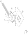
- the Figure 1 shows an embodiment of a photonic component 10 in an exploded view obliquely from the side.
- the Figure 2 shows components of the photonic device 10 according to Figure 1 in more detail. Below we will refer to the Figures 1 and 2 referred to jointly.
- the photonic component 10 has a first chip, which is a photonically integrated chip 1.
- a second chip 2 adjoins the photonically integrated chip 1, which in turn adjoins a third chip, hereinafter referred to as intermediate chip 3, on its side facing away from the photonically integrated chip 1.
- a fourth chip 4 is adjacent to a fifth chip, which forms a fiber holder 5 of the photonic component 10.
- a guide pin 40 preferably a metal pin
- the photonically integrated chip 1 is preferably provided with aligned positioning holes, preferably in the form of blind holes, into which the guide pins 40 can engage.
- the fourth chip 4, the fifth chip (the fiber holder 5) and the guide pins 40 form in the embodiment according to the Figures 1 and 2 preferably a prefabricated unit in the form of a plug 50.
- the photonically integrated chip 1, the second chip 2 and the intermediate chip 3 preferably form a prefabricated connector receptacle 60 into which the connector 50 can be inserted with its guide pins 40.
- the guide pins 40 are inserted into the through holes 21 in the chips 2 and 3 and into the positioning holes in the photonically integrated chip 1.
- the fiber holder 5 serves to hold fibers 30, which are preferably single-mode fibers.
- the third chip or the intermediate chip 3 and the fourth chip 4 lie directly on top of one another, so that the chips 2, 3 and 4 form a chip stack 20 with chips lying on top of one another.
- the chip stack 20 is delimited on the outside by the photonically integrated chip 1 and the fiber holder 5.
- the photonically integrated chip 1 of the connector receptacle 60 is preferably equipped with contacts on the outer side facing away from the chip stack 20, which contacts enable a chip connection to an electrical circuit board 70.
- the circuit board 70 is preferably mounted on an electrical carrier board 90.
- the circuit board 70 preferably has contacts for mounting on the electrical carrier board 90 that are suitable for a ball grid array solder connection.
- the contacts are located on the underside 71 of the circuit board 70 facing away from the photonically integrated chip 1.
- the Figure 1 also shows a support element 80 which is placed on the circuit board 70.
- the support element 80 is preferably formed by a casting compound and preferably has two functions: One of the two functions is to support the fibers 30 or a support plate 81 (for example in the form of a sixth chip) provided for holding the fibers 30 on the fiber holder 5.
- the support element 80 preferably has a suitable groove 82.
- the other of the two functions of the support element 80 is to effect a pre-adjustment of the plug 50 relative to the plug receptacle 60 when the plug 50 is to be inserted into the plug receptacle 60.
- the support element 80 is designed to be ring-shaped.
- the support element 80 is more clearly visible in the Figure 3 It can be seen that the inner wall 83 of the ring formed by the support element 80 has an upper region 83a which tapers in a funnel shape and thus, when the plug 50 is inserted, causes a relative adjustment of the plug relative to the inner region of the support element 80 and the plug receptacle 60 located therein.
- the inner wall 83 lies laterally on the plug receptacle 60 located therein (cf. Figures 1 and 2 ).
- the inner wall 83 of the support element 80 is preferably perpendicular to the surface plane of the circuit board 70 located underneath.
- the Figure 1 also shows a carrier ring 100, in the inner ring area of which the electrical carrier plate 90 with the support element 80 located thereon is inserted.
- the carrier ring 100 serves, for example, to support a not shown heat sink, which cools or "cools" the circuit board 70 and the electrical carrier board 90.
- the support element 80 is preferably formed by pouring the inner ring area between the plug receptacle 60 and the inner edge of the carrier ring 100.
- the upper area 83a of the inner wall 83 can be formed, for example, by a demolding slope of the potting compound forming the support element 80.
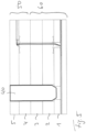
- the Figure 4 shows the plug 50 and the plug receptacle 60 according to the Figures 1 and 2 in more detail.
- the connector 50 is formed by the guide pins 40, the fourth chip 4 and the fifth chip above it (fiber holder 5).
- the fibers 30 are connected to the connector 50 according to Figure 2 , of which only one is visible in the cross-sectional view according to Figure 4. It can be seen that the fiber 30 lies in a V-groove 51 which is etched into the silicon material of the fiber holder 5.
- the fiber holder 5 In order to deflect radiation that is coupled out of or into the fiber 30, the fiber holder 5 has an associated deflection mirror 52 for each of the fibers 30, which is formed by a mirror surface etched anisotropically into the silicon material of the fifth chip or the fiber holder 5.
- first lens 200 a lens, hereinafter referred to as the first lens 200, can be seen, which is inserted into the outer surface 4a of the fourth chip 4 adjacent to the fiber holder 5. introduced, preferably etched.
- further first lenses can also be introduced, in particular etched, into the outer surface 4a, for example for radiation in or from another of the fibers which are in the Figures 1 and 2 are shown.
- the first lens 200 cooperates with a second lens 210, which is introduced, in particular etched, into the outer surface 2a of the second chip 2 adjacent to the photonically integrated chip 1.
- a second lens 210 is introduced, in particular etched, into the outer surface 2a of the second chip 2 adjacent to the photonically integrated chip 1.
- further second lenses can be introduced, in particular etched, into the outer surface 2a, again for example for radiation in or from another of the fibers that are in the Figures 1 and 2 are shown.
- the first lens 200 and the second lens 210 are preferably located directly opposite one another and preferably form a common beam path SW; on the beam path SW, the radiation between the two lenses 200 and 210 preferably forms a collimated beam.
- the lenses 200 and 210 are preferably converging lenses.
- the Figure 4 also shows the structure of the photonically integrated chip 1 in more detail.
- the photonically integrated chip 1 has a substrate 300, preferably a silicon substrate, whose substrate back 301 is connected to the Figure 4 borders the second chip 2 located above it.
- the substrate 300 is provided with a blind hole 310 that extends from the substrate rear side 301 to a separating layer 311 that is applied to the substrate front side 302 of the substrate 300.
- the separating layer 311 is preferably SiO2 material.
- a wave-guiding material layer 320 made of preferably silicon. Radiation which is emitted from the wave-guiding material layer 320 by means of a Figure 4
- the radiation S is coupled out in the direction of the substrate 300 by a deflection unit (not shown in detail), passes through the blind hole 310 and is directed by means of the second lens 210 in the direction of the first lens 200.
- the first lens 200 directs the radiation S onto the deflection mirror 52, which couples the radiation S into the fiber 30.
- Radiation from the fiber 30 passes through the deflection mirror, the first lens 200, the second lens 210, the blind hole 310 and the deflection unit in a corresponding manner into the wave-guiding material layer 320.
- the Figure 4 also shows the structure of the connector receptacle 60 in more detail. It can be seen that the second chip 2 and the third chip (intermediate chip 3) are each provided with a through hole 21 through which a chamfered pin end 41 of the guide pin 40 can be pushed in the direction of the substrate 30 of the photonically integrated chip 1.
- the substrate 300 of the photonically integrated chip 1 has positioning holes 22 in the form of blind holes 310, into which the chamfered pin end 41 of a guide pin 40 can be inserted in order to ensure an adjustment of the connector 50 not only relative to the second and third chip, but also relative to the photonically integrated chip 1.
- the chamfered pin ends 41 facilitate the insertion of the guide pins 40 and the centering of the Guide pins 40 in the through holes 21 or the positioning holes 22.
- the Figure 5 shows the plug 50 and the plug receptacle 60 according to Figure 4 after the connector 50 with its guide pins 40 has been completely inserted into the connector receptacle 60. This can be seen from the fact that the pin ends 41 of the guide pins 40 have reached the respective positioning hole 22 in the substrate 300 of the photonically integrated chip.
- the chips 2 to 4 form the chip stack 20 according to Figure 2 .
- the fourth chip 4 and the fifth chip are preferably connected to one another without adhesive and/or soldering to form the connector 50, in particular by van der Waals bonding or thermal fusion bonding.
- the photonically integrated chip 1, the second chip 2 and the third chip (intermediate chip 3) are preferably also connected to one another without adhesive and/or soldering to form the connector receptacle 60, in particular by van der Waals bonding or thermal fusion bonding.
- the outside of the plug 50 which in the embodiment according to the Figures 1 to 4 formed by the outer surface of the fourth chip 4 facing the connector receptacle 60, is preferably flat and coated with an anti-reflection layer.
- the outer side of the third chip (intermediate chip 3) facing the fourth chip is also flat and coated with an anti-reflection layer.
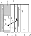
- the Figure 6 shows the already mentioned in connection with the Figure 4
- the structure of the photonic integrated chip 1 explained in more detail.
- the Figure 6 an intermediate layer 330 which is applied to the side of the shaft-guiding material layer 320 facing away from the blind hole 310.
- the intermediate layer 330 has a thickness H and separates the wave-guiding material layer 320 from a mirror layer 340 (e.g. metal layer) which is arranged on the side of the intermediate layer 330 facing away from the blind hole 310.
- a mirror layer 340 e.g. metal layer
- the Figure 6 further shows a coupler 350 formed in the wave-guiding material layer 320 or connected to an optical waveguide 360 formed in the wave-guiding material layer 320.
- the coupler 350 and the mirror layer 340 form a deflection unit 370 that can deflect radiation from the waveguide 360 in the direction of the blind hole 310 or in the direction of the second lens 210.
- the deflection unit 370 can couple radiation that comes from the second lens 210 or the blind hole 310 into the wave-guiding material layer 320 or into the optical waveguide 360.
- the coupling and decoupling in the direction of the blind hole 310 or the wave-guiding material layer 320 takes place partly directly and partly indirectly via the mirror layer 340 or indirectly, as in Figure 6 indicated by arrows.
- further mirror and/or metal layers can be integrated to form the deflection unit 370 and/or for other purposes.
Landscapes
- Physics & Mathematics (AREA)
- General Physics & Mathematics (AREA)
- Optics & Photonics (AREA)
- Optical Couplings Of Light Guides (AREA)
Description
- Die Erfindung bezieht sich auf ein photonisches Bauelement mit einem photonisch integrierten Chip und einer mit dem photonisch integrierten Chip mechanisch verbundenen Faserhalterung, wobei die Faserhalterung aufweist: zumindest eine Nut, in die eine optische Faser, insbesondere Monomodefaser, eingelegt ist, und zumindest eine Spiegelfläche, die Strahlung der Faser in Richtung des photonisch integrierten Chips und/oder Strahlung des photonisch integrierten Chips in Richtung der Faser spiegelt. Ein derartiges Bauelement ist aus der deutschen Patentschrift
DE 44 45 997 und auch aus der japanischen DruckschriftJP 2011 017928 A - Andere optische Bauelemente sind in den Druckschriften
JP 2011 017925 A WO 2016/148896 A1 ,US 2006/280410 A1 ,WO 2016/140855 A1 ,WO 2012/158671 A1 undUS 2016/0282570 A1 offenbart. - Der Erfindung liegt die Aufgabe zugrunde, ein photonisches Bauelement anzugeben, das sich kostengünstig fertigen lässt und einen möglichst kompakten Aufbau aufweist.
- Diese Aufgabe wird erfindungsgemäß durch ein photonisches Bauelement mit den Merkmalen gemäß Patentanspruch 1 gelöst. Vorteilhafte Ausgestaltungen des erfindungsgemäßen Bauelements sind in Unteransprüchen angegeben.
- Ein wesentlicher Vorteil des erfindungsgemäßen Bauelements ist darin zu sehen, dass der Chipstapel, die Durchgangslöcher und die Führungsstifte gemeinsam eine einfache, automatische Justage der Faserhalterung ermöglichen, insbesondere beispielsweise mit Blick auf eine oder mehrere Linsen im Strahlweg zwischen der Faserhalterung und dem photonisch integrierten Chip.
- Mit Blick auf eine einfache Justage bezüglich des photonisch integrierten Chips wird es als vorteilhaft angesehen, wenn durch die zumindest zwei Durchgangslöcher des Chipstapels jeweils ein Führungsstift hindurchgeführt ist, der sich in ein zugeordnetes Positionierloch in der Faserhalterung und ein zugeordnetes Positionierloch in dem photonisch integrierten Chip erstreckt und den photonisch integrierten Chip, den Chipstapel und die Faserhalterung relativ zueinander positioniert.
- Die Durchgangslöcher des Chipstapels und die zugeordneten Positionierlöcher fluchten vorzugsweise.
- Die Positionierlöcher in der Faserhalterung sind vorzugsweise Durchgangslöcher; diese Ausgestaltung ermöglicht ein Einführen der Führungsstifte von außen in die Faserhalterung hinein.
- Mit Blick auf die Strahlführung optischer Strahlung zwischen der Faserhalterung und dem photonisch integrierten Chip wird es als vorteilhaft angesehen, wenn der Chip des Chipstapels, der an die Faserhalterung grenzt, an seiner der Faserhalterung zugewandten Chipseite mit mindestens einer Linse, nachfolgend erste Linse des Chipstapels genannt, versehen ist, der Chip des Chipstapels, der an den photonisch integrierten Chip grenzt, an seiner dem photonisch integrierten Chip zugewandten Chipseite ebenfalls mit mindestens einer Linse, nachfolgend zweite Linse des Chipstapels genannt, versehen ist und die erste und zweite Linse einen gemeinsamen Strahlweg durch den Chipstapel begrenzen.
- Die erste und zweite Linse liegen vorzugsweise einander gegenüber.
- Die Abweichung zwischen der optischen Weglänge zwischen der Linsenoberfläche der ersten Linse und der Faser und der optischen Weglänge zwischen der Linsenoberfläche der zweiten Linse und einem Koppler des photonisch integrierten Chips ist vorzugsweise kleiner als 5 % und/oder kleiner als die doppelte Rayleighlänge des durch die erste Linse fokussierten Strahls.
- Die Chips des Chipstapels, des photonisch integrierten Chips und die Faserhalterung sind bevorzugt Siliziumchips.
- Der Chipstapel weist vorzugsweise zumindest einen Zwischenchip auf, der zwischen den beiden bereits erwähnten äußeren Chips des Chipstapels angeordnet ist und ebenfalls zumindest zwei zugeordnete Durchgangslöcher für die Führungsstifte aufweist. Die Dicke des Zwischenchips beträgt vorzugsweise mindestens 500 µm, damit der Steckkontakt für die Führungsstifte genug Tiefe vorhält, so dass der Steckvorgang für einen Anwender gut fühlbar ist.
- Der oder die Zwischenchips bilden bevorzugt einen Bestandteil des Steckers oder der Steckeraufnahme.
- Die auf der Steckeraufnahme aufliegende Steckerfläche des Steckers ist bevorzugt plan, wobei die Steckerfläche durch die der Steckeraufnahme zugewandte Oberfläche desjenigen Chips, der an die Faserhalterung grenzt, oder des oder eines der Zwischenchips gebildet ist.
- Die auf dem Stecker aufliegende Fläche der Steckeraufnahme ist vorzugsweise plan, wobei diese Fläche durch die dem Stecker zugewandte Oberfläche desjenigen Chips, der an den photonisch integrierten Chip grenzt, oder des oder eines der Zwischenchips gebildet ist.
- Besonders vorteilhaft ist es, wenn die inneren, aufeinander liegenden Flächen der Chips des Chipstapels plan sind und die erste und zweite Linse in die Oberflächen auf den Außenseiten des Chipstapels eingebracht, insbesondere eingeätzt sind.
- Die beiden Linsen weisen vorzugsweise die gleiche Fokuslänge auf. Besonders bevorzugt sind sie identisch.
- Der Chip, der an die Faserhalterung grenzt, und der Chip, der an den photonisch integrierten Chip grenzt, sind mit Blick auf eine geringe Teilezahl und niedrige Herstellungskosten vorzugsweise identisch.
- Bezüglich der Linsenausgestaltung wird es als vorteilhaft angesehen, wenn die erste Linse des Chipstapels derart ausgebildet ist, dass Strahlung von der Faserhalterung als kollimierter Strahl zu der zweiten Linse gelenkt wird, und die zweite Linse des Chipstapels derart ausgebildet ist, dass Strahlung von dem photonisch integrierten Chip als kollimierter Strahl zu der ersten Linse des Chipstapels gelenkt wird.
- Der Strahlweg zwischen der ersten und der zweiten Linse verläuft vorzugsweise senkrecht zu den planen Grenzflächen zwischen den Chips des Chipstapels.
- Der photonisch integrierte Chip weist bevorzugt auf: ein Substrat, dessen Substratgrundmaterial ein Halbleitermaterial, insbesondere Silizium ist, einen integrierten optischen Wellenleiter, der in zumindest einer auf dem Substrat befindlichen wellenführenden Materialschicht des Chips integriert ist, eine Umlenkeinheit, und ein Sackloch, das sich von der Substratrückseite bis zu einer das Substrat und die wellenführende Materialschicht trennenden Trennschicht erstreckt, wobei die Umlenkeinheit Strahlung des Wellenleiters aus der Ebene der wellenführenden Materialschicht in Richtung Sackloch und Substratrückseite umlenkt und Strahlung, die aus dem Chipstapel kommt und das Sackloch und die Trennschicht passiert hat, in die Ebene der wellenführenden Materialschicht umlenkt.
- Die Umlenkeinheit umfasst bevorzugt einen in dem optischen Wellenleiter ausgebildeten oder mit dem optischen Wellenleiter in Verbindung stehenden Koppler und eine Spiegelschicht, die sich unmittelbar auf der dem Sackloch abgewandten Seite der wellenführenden Materialschicht, auf einer auf der dem Sackloch abgewandten Seite der wellenführenden Materialschicht aufliegenden Zwischenschicht oder auf einem auf der dem Sackloch abgewandten Seite der wellenführenden Materialschicht aufliegenden Zwischenschichtstapel befindet.
- Der Koppler lenkt bevorzugt Strahlung des Wellenleiters zum Teil aus der Ebene der wellenführenden Materialschicht heraus ganz oder zumindest zum Teil in Richtung auf die Spiegelschicht um.
- Die Spiegelschicht, das Sackloch und der Koppler sind vorzugsweise derart angeordnet und ausgestaltet, dass der in Richtung auf die Spiegelschicht umgelenkte Teil der Strahlung von der Spiegelschicht in Richtung Sackloch gespiegelt wird.
- Das Positionierloch in dem photonisch integrierten Chip ist bevorzugt ein Sackloch, insbesondere ein Sackloch, das sich von der Substratrückseite bis zu einer das Substrat und die wellenführende Materialschicht trennenden Trennschicht erstreckt.
- Die Führungsstifte weisen vorzugsweise jeweils ein angefastes Stiftende auf.
- Das Bauelement weist vorzugsweise ein Stützelement auf, auf dem die Faser und/oder ein an der Faser angebrachtes Stützplättchen aufliegt.
- Das Stützelement bildet vorzugsweise einen Ring. Die Innenwand des Rings verjüngt sich bevorzugt in einem oberen Bereich, in den der Stecker eingeführt ist, trichterförmig und bewirkt zumindest dort eine Vorjustage des Steckers relativ zur Steckeraufnahme beim Einführen des Steckers.
- In einem unteren Bereich der Innenwand, in dem sich die Steckeraufnahme befindet, liegt die Innenwand vorzugsweise an der Steckeraufnahme seitlich an.
- Auch ist es vorteilhaft, wenn das Stützelement eine Nut aufweist und die Faser oder das an der Faser angebrachte Stützplättchen in der Nut auf dem Stützelement aufliegt.
- Das Stützelement wird vorzugsweise durch eine Vergussmasse gebildet.
- Bezüglich der Fasermontage ist es vorteilhaft, wenn die Nut in der Faserhalterung eine in Silizium anisotrop geätzte V-Nut ist und ein der Faser zugeordneter Umlenkspiegel in der Faserhalterung durch eine anisotrop in das Silizium geätzte Fläche gebildet ist.
- Der Strahlweg zwischen der ersten und der zweiten Linse trifft auf die erste und/oder zweite Linse vorzugsweise nicht zentrisch, sondern versetzt zum jeweiligen Linsenzentrum.
- Die Azentrizität des Strahlwegs relativ zur ersten und zweiten Linse ist bei der ersten Linse vorzugsweise anders als bei der zweiten Linse. Eine solche unterschiedliche Azentrizität erlaubt eine linsenindividuelle Optimierung des Abbildungsverhaltens der Linse.
- Die erste und/oder zweite Linse sind bevorzugt Asphären.
- Die erste und/oder zweite Linse sind vorzugsweise elliptisch.
- Die erste und/oder zweite Linse sind bevorzugt mit einer Anti-Reflex Schicht beschichtet.
- Zumindest zwei unmittelbar aufeinander liegende Flächen der Chips des Chipstapels, insbesondere die Außenseite des Steckers und die Außenseite der Steckeraufnahme, sind vorzugsweise jeweils mit einer Anti-Reflex Schicht beschichtet.
- Die Chips des Steckers und die Chips der Steckeraufnahme sind vorzugsweise klebstoff- und/oder lotfrei, insbesondere durch Van-der-Waals Bonding oder Thermal Fusion Bonding, miteinander verbunden. Eine Verbindung ohne Klebstoff gewährleistet eine optimale Wärmeleitung und der transmittierte Strahl erfährt keine Fresnelverluste.
- Darüber hinaus ist es vorteilhaft, wenn der photonisch integrierte Chip auf der dem Chipstapel abgewandten Außenseite Kontakte für Flipchipverbindungen aufweist und der photonisch integrierte Chip auf einer Leiterplatte mit einem Flipchip-Verfahren gebondet und mit der Leiterplatte elektrisch verbunden ist. Durch die Separation von elektrischen und optischen Kontakten auf die Ober- und Unterseite des photonisch integrierten Chips steht auf der dortigen Chipunterseite mehr Platz für die Verbindung des photonisch integrierten Chips mit dem Chipstapel zur Verfügung als in einer alternativen Variante, bei der die optische Kontaktierung ebenfalls auf der Chipoberseite durchgeführt wird. Durch die vergrößerte Auflagefläche erhöht sich die mechanische Stabilität des Chipstapels.
- Die Leiterplatte bildet vorzugsweise einen Träger für das Stützelement. Das Stützelement stabilisiert den Chipstapel zusammen mit der Faserhalterung mechanisch, wodurch geringere Verformungen und somit eine robustere optische Kopplung erreicht werden können.
- Die Leiterplatte weist auf ihrer dem Stützelement abgewandten Unterseite vorzugsweise Kontakte für eine BGA (Ball-Grid-Array)-Lötverbindung auf.
- Die Erfindung wird nachfolgend anhand von Ausführungsbeispielen näher erläutert; dabei zeigen beispielhaft
- Figur 1
- ein Ausführungsbeispiel für ein erfindungsgemäßes optisches Bauelement in einer Explosionsdarstellung schräg von der Seite,
- Figur 2
- Bestandteile des photonischen Bauelements gemäß Figur 1 näher im Detail,
- Figur 3
- ein Stützelement des photonischen Bauelements gemäß
Figur 1 in einer dreidimensionalen Darstellung schräg von der Seite näher im Detail, - Figur 4
- einen Stecker und eine Steckeraufnahme des photonischen Bauelements gemäß
Figur 1 in einem Querschnitt, wobei dieFigur 4 einen Zustand während des Einschiebens des Steckers in die Steckeraufnahme zeigt, - Figur 5
- den Stecker und die Steckeraufnahme gemäß
Figur 4 , nachdem der Stecker vollständig in die Steckeraufnahme eingeführt worden ist, und - Figur 6
- ein Ausführungsbeispiel für eine vorteilhafte Ausgestaltung eines photonisch integrierten Chips des photonischen Bauelements gemäß
Figur 1 näher im Detail. - In den Figuren werden Übersicht halber für identische oder vergleichbare Komponenten stets dieselben Bezugszeichen verwendet.
- Die
Figur 1 zeigt ein Ausführungsbeispiel für ein photonisches Bauelement 10 in einer Explosionsdarstellung schräg von der Seite. DieFigur 2 zeigt Komponenten des photonischen Bauelements 10 gemäßFigur 1 näher im Detail. Nachfolgend wird auf dieFiguren 1 und2 gemeinsam Bezug genommen. - Das photonische Bauelement 10 weist einen ersten Chip auf, bei dem es sich um einen photonisch integrierten Chip 1 handelt. An den photonisch integrierten Chip 1 grenzt ein zweiter Chip 2 an, der wiederum auf seiner dem photonisch integrierten Chip 1 abgewandten Seite an einen dritten Chip, nachfolgend Zwischenchip 3 genannt, angrenzt.
- Ein vierter Chip 4 grenzt an einen fünften Chip, der eine Faserhalterung 5 des photonischen Bauelements 10 bildet.
- Zur relativen Montage des zweiten, dritten, vierten und fünften Chips relativ zueinander, sind diese mit Durchgangslöchern 21 versehen, in die jeweils ein Führungsstift 40, vorzugsweise Metallstift, eingeschoben werden kann.
- Um eine relative Justage auch zum photonisch integrierten Chip 1 mittels der Führungsstifte 40 zu ermöglichen, ist der photonisch integrierte Chip 1 vorzugweise mit fluchtenden Positionierlöchern, vorzugsweise in Form von Sacklöchern, versehen, in die die Führungsstifte 40 eingreifen können.
- Der vierte Chip 4, der fünfte Chip (die Faserhalterung 5) und die Führungsstifte 40 bilden bei der Ausführungsform gemäß den
Figuren 1 und2 vorzugsweise eine vorgefertigte Einheit in Form eines Steckers 50. - Der photonisch integrierte Chip 1, der zweite Chip 2 und der Zwischenchip 3 bilden vorzugsweise eine vorgefertigte Steckeraufnahme 60, in die der Stecker 50 mit seinen Führungsstiften 40 eingeschoben werden kann. Die Führungsstifte 40 werden dabei in die Durchgangslöcher 21 in den Chips 2 und 3 sowie in die Positionierlöcher im photonisch integrierten Chip 1 eingeschoben.
- Die Faserhalterung 5 dient zum Halten von Fasern 30, bei denen es sich vorzugsweise um Monomodefasern handelt.
- Ist der Stecker 50 in die Steckeraufnahme 60 eingeschoben, so liegen der dritte Chip bzw. der Zwischenchip 3 und der vierte Chip 4 unmittelbar aufeinander, so dass die Chips 2, 3 und 4 einen Chipstapel 20 mit aufeinanderliegenden Chips bilden. Der Chipstapel 20 wird außen von dem photonisch integrierten Chip 1 und der Faserhalterung 5 begrenzt.
- Der photonisch integrierte Chip 1 der Steckeraufnahme 60 ist auf der dem Chipstapel 20 abgewandten Außenseite vorzugsweise mit Kontakten ausgestattet, die eine Chipverbindung mit einer elektrischen Leiterplatte 70 ermöglichen.
- Die Leiterplatte 70 wird vorzugsweise auf einer elektrischen Trägerplatte 90 montiert. Die Leiterplatte 70 weist zur Montage auf der elektrischen Trägerplatte 90 vorzugsweise Kontakte auf, die für eine Ball-Grid-Array-Löt-Verbindung geeignet sind. Die Kontakte befinden sich auf der dem photonisch integrierten Chip 1 abgewandten Unterseite 71 der Leiterplatte 70.
- Die
Figur 1 zeigt darüber hinaus ein Stützelement 80, das auf die Leiterplatte 70 aufgesetzt ist. Das Stützelement 80 wird vorzugsweise durch eine Vergussmasse gebildet und hat vorzugsweise zwei Funktionen: Eine der beiden Funktionen besteht darin, die Fasern 30 bzw. ein zum Halten der Fasern 30 an der Faserhalterung 5 vorgesehenes Stützplättchen 81 (zum Beispiel in Form eines sechsten Chips) abzustützen. Hierfür weist das Stützelement 80 vorzugsweise eine geeignete Nut 82 auf. Die andere der beiden Funktionen des Stützelements 80 besteht darin, eine Vorjustage des Steckers 50 relativ zur Steckeraufnahme 60 zu bewirken, wenn der Stecker 50 in die Steckeraufnahme 60 eingeführt werden soll. Zu diesem Zweck ist das Stützelement 80 ringförmig ausgebildet. - Das Stützelement 80 ist deutlicher in der
Figur 3 dargestellt. Es lässt sich erkennen, dass die Innenwand 83 des durch das Stützelement 80 gebildeten Rings einen oberen Bereich 83a aufweist, der sich trichterförmig verjüngt und somit beim Einführen des Steckers 50 eine relative Justage des Steckers relativ zu dem Innenbereich des Stützelements 80 und der darin befindlichen Steckeraufnahme 60 bewirkt. - In einem unteren Bereich 83b liegt die Innenwand 83 seitlich an der darin befindlichen Steckeraufnahme 60 (vgl.
Figuren 1 und2 ) an. Im unteren Bereich 83b steht die Innenwand 83 des Stützelements 80 vorzugsweise senkrecht auf der Oberflächenebene der darunter befindlichen Leiterplatte 70. - Die
Figur 1 zeigt darüber hinaus einen Trägerring 100, in dessen Innenringbereich die elektrische Trägerplatte 90 mit dem darauf befindlichen Stützelement 80 eingesetzt sind. Der Trägerring 100 dient beispielsweise dazu, einen in den Figuren nicht gezeigten Kühlkörper zu tragen, der die Leiterplatte 70 und die elektrische Trägerplatte 90 kühlt bzw. "entwärmt". - Das Stützelement 80 wird vorzugsweise durch Ausgießen des Innenringbereichs zwischen der Steckeraufnahme 60 und dem Innenrand des Trägerrings 100 gebildet. Der obere Bereich 83a der Innenwand 83 kann beispielsweise durch eine Entformungsschräge der das Stützelement 80 bildenden Vergussmasse gebildet sein.
- Die
Figur 4 zeigt den Stecker 50 und die Steckeraufnahme 60 gemäß denFiguren 1 und2 näher im Detail. - In der
Figur 4 lässt sich erkennen, dass der Stecker 50 durch die Führungsstifte 40, den vierten Chip 4 sowie den darüber befindlichen fünften Chip (Faserhalterung 5) gebildet wird. An den Stecker 50 sind die Fasern 30 gemäßFigur 2 angeschlossen, von denen in der Querschnittsdarstellung gemäß Figur 4 nur eine einzige erkennbar ist. Man sieht, dass die Faser 30 in einer V-Nut 51 liegt, die in das Siliziummaterial der Faserhalterung 5 eingeätzt ist. - Zur Umlenkung von Strahlung, die aus der Faser 30 ausgekoppelt bzw. in diese eingekoppelt wird, weist die Faserhalterung 5 für jede der Fasern 30 jeweils einen zugeordneten Umlenkspiegel 52 auf, der durch eine anisotrop in das Siliziummaterial des fünften Chips bzw. der Faserhalterung 5 geätzte Spiegelfläche gebildet ist.
- In der
Figur 4 lässt sich darüber hinaus eine Linse, nachfolgend erste Linse 200 genannt, erkennen, die in die an die Faserhalterung 5 angrenzende Außenfläche 4a des vierten Chips 4 eingebracht, vorzugsweise eingeätzt, ist. Zusätzlich zu der ersten Linse 200 können in die Außenfläche 4a auch weitere erste Linsen eingebracht, insbesondere eingeätzt, sein, beispielsweise für Strahlung in oder aus einer anderen der Fasern, die in denFiguren 1 und2 gezeigt sind. - Die erste Linse 200 kooperiert mit einer zweiten Linse 210, die an der an den photonisch integrierten Chip 1 angrenzenden Außenfläche 2a des zweiten Chips 2 eingebracht, insbesondere eingeätzt, ist. An der Außenfläche 2a können neben der zweiten Linse 210 noch weitere zweite Linsen eingebracht, insbesondere eingeätzt, wiederum beispielsweise für Strahlung in oder aus einer anderen der Fasern, die in den
Figuren 1 und2 gezeigt sind. - Die erste Linse 200 und die zweite Linse 210 liegen vorzugsweise einander unmittelbar gegenüber und bilden vorzugsweise einen gemeinsamen Strahlweg SW; auf dem Strahlweg SW formt die Strahlung zwischen den beiden Linsen 200 und 210 vorzugsweise einen kollimierten Strahl. Bei den Linsen 200 und 210 handelt es sich vorzugsweise um Sammellinsen.
- Die
Figur 4 lässt darüber hinaus den Aufbau des photonisch integrierten Chips 1 näher erkennen. Der photonisch integrierte Chip 1 weist ein Substrat 300, vorzugsweise ein Siliziumsubstrat, auf, dessen Substratrückseite 301 an den in derFigur 4 darüber befindlichen zweiten Chip 2 grenzt. Im Bereich der zweiten Linse 210 ist das Substrat 300 mit einem Sackloch 310 versehen, das sich von der Substratrückseite 301 bis zu einer Trennschicht 311 erstreckt, die auf der Substratvorderseite 302 des Substrats 300 aufgebracht ist. Bei der Trennschicht 311 handelt es sich vorzugsweise um SiO2-Material. - Auf der dem Sackloch 310 abgewandten Seite der Trennschicht 311 befindet sich eine wellenführende Materialschicht 320 aus vorzugsweise Silizium. Strahlung, die aus der wellenführenden Materialschicht 320 mittels einer in der
Figur 4 nicht näher gezeigten Umlenkeinheit in Richtung des Substrats 300 ausgekoppelt wird, passiert das Sackloch 310 und wird mittels der zweiten Linse 210 in Richtung auf die erste Linse 200 gelenkt. Die erste Linse 200 lenkt die Strahlung S auf den Umlenkspiegel 52, der die Strahlung S in die Faser 30 einkoppelt. - Strahlung der Faser 30 gelangt über den Umlenkspiegel, die erste Linse 200, die zweite Linse 210, das Sackloch 310 sowie die Umlenkeinheit in entsprechender Weise in die wellenführende Materialschicht 320.
- Die
Figur 4 zeigt darüber hinaus den Aufbau der Steckeraufnahme 60 näher im Detail. Es lässt sich erkennen, dass der zweite Chip 2 und der dritte Chip (Zwischenchip 3) jeweils mit einem Durchgangsloch 21 versehen sind, durch die ein angefastes Stiftende 41 des Führungsstifts 40 in Richtung auf das Substrat 30 des photonisch integrierten Chips 1 geschoben werden kann. - Vorzugsweise weist das Substrat 300 des photonisch integrierten Chips 1 Positionierlöcher 22 in Form von Sacklöchern 310 auf, in die jeweils das angefaste Stiftende 41 eines Führungsstifts 40 eingeschoben werden kann, um eine Justage des Steckers 50 nicht nur relativ zum zweiten und dritten Chip, sondern auch relativ zum photonisch integrierten Chip 1 sicherzustellen. Die angefasten Stiftenden 41 erleichtern das Einführen der Führungsstifte 40 sowie die Zentrierung der Führungsstifte 40 in den Durchgangslöchern 21 bzw. den Positionierlöchern 22.
- Die
Figur 5 zeigt den Stecker 50 und die Steckeraufnahme 60 gemäßFigur 4 , nachdem der Stecker 50 mit seinen Führungsstiften 40 vollständig in die Steckeraufnahme 60 eingeführt worden ist. Das lässt sich daran erkennen, dass die Stiftenden 41 der Führungsstifte 40 das jeweilige Positionierloch 22 im Substrat 300 des photonisch integrierten Chips erreicht haben. - Nach dem Zusammenstecken von Stecker 50 und Steckeraufnahme 60 bilden die Chips 2 bis 4 den Chipstapel 20 gemäß
Figur 2 . - Der vierte Chip 4 und der fünfte Chip (die Faserhalterung 5) sind zur Bildung des Steckers 50 vorzugsweise klebstoff- und/oder lötfrei miteinander verbunden, insbesondere durch Van-der-Waals Bonding oder Thermal-Fusion Bonding.
- Der photonisch integrierte Chip 1, der zweite Chip 2 und der dritte Chip (Zwischenchip 3) sind zur Bildung der Steckeraufnahme 60 vorzugsweise ebenfalls klebstoff- und/oder lötfrei miteinander verbunden, insbesondere durch Van-der-Waals Bonding oder Thermal-Fusion Bonding.
- Die Außenseite des Steckers 50, die bei dem Ausführungsbeispiel gemäß den
Figuren 1 bis 4 durch die der Steckeraufnahme 60 zugewandten Außenfläche des vierten Chips 4 gebildet ist, ist vorzugsweise plan und mit einer Antireflexionsschicht beschichtet. In entsprechender Weise ist es vorteilhaft, wenn auch die dem vierten Chip zugewandte Außenseite des dritten Chips (Zwischenchips 3) plan ist und mit einer Antireflexionsschicht beschichtet ist. - Die
Figur 6 zeigt den bereits im Zusammenhang mit derFigur 4 erläuterten Aufbau des photonisch integrierten Chips 1 näher im Detail. Man erkennt das Substrat 300, die Trennschicht 311 und die wellenführende Materialschicht 320, die bereits im Zusammenhang mit derFigur 4 erläutert worden sind. Darüber hinaus erkennt man in derFigur 6 eine Zwischenschicht 330, die auf der dem Sackloch 310 abgewandten Seite der wellenführenden Materialschicht 320 aufgebracht ist. - Die Zwischenschicht 330 weist eine Dicke H auf und trennt die wellenführende Materialschicht 320 von einer Spiegelschicht 340 (z. B. Metallschicht), die auf der dem Sackloch 310 abgewandten Seite der Zwischenschicht 330 angeordnet ist.
- Die
Figur 6 zeigt darüber hinaus einen Koppler 350, der in der wellenführenden Materialschicht 320 ausgebildet oder mit einem in der wellenführenden Materialschicht 320 ausgebildeten optischen Wellenleiter 360 in Verbindung steht. - Der Koppler 350 und die Spiegelschicht 340 bilden eine Umlenkeinheit 370, die Strahlung vom Wellenleiter 360 in Richtung des Sacklochs 310 bzw. in Richtung der zweiten Linse 210 umlenken kann. In entsprechender Weise kann die Umlenkeinheit 370 Strahlung, die von der zweiten Linse 210 bzw. dem Sackloch 310 kommt, in die wellenführende Materialschicht 320 bzw. in den optischen Wellenleiter 360 einkoppeln. Das Ein- und Auskoppeln in Richtung Sackloch 310 bzw. wellenführende Materialschicht 320 erfolgt zum Teil unmittelbar bzw. direkt und zum Teil mittelbar über die Spiegelschicht 340 bzw. indirekt, wie in
Figur 6 durch Pfeile angedeutet ist. - Im Backend-of-Line 380, also in weiteren Schichten auf der Oberseite des photonisch integrierten Chips 1, können zur Bildung der Umlenkeinheit 370 und/oder zu anderen Zwecken weitere Spiegel- und/oder Metallschichten integriert sein.
Claims (12)
- Photonisches Bauelement (10) mit einem photonisch integrierten Chip (1) und einer mit dem photonisch integrierten Chip (1) mechanisch verbundenen Faserhalterung (5), wobei die Faserhalterung (5) aufweist:- zumindest eine Nut (52), in die eine optische Faser (30), insbesondere Monomodefaser, eingelegt ist, und- zumindest eine Spiegelfläche (52), die Strahlung (S) der Faser (30) in Richtung des photonisch integrierten Chips (1) und/oder Strahlung (S) des photonisch integrierten Chips (1) in Richtung der Faser (30) spiegelt,wobei- zwischen dem photonisch integrierten Chip (1) und der Faserhalterung (5) ein Chipstapel (20) mit zumindest zwei Chips angeordnet ist, von denen einer an die Faserhalterung (5) grenzt und einer an den photonisch integrierten Chip (1),- der Chipstapel (20) mit zumindest zwei Durchgangslöchern (21) versehen ist,- durch die zumindest zwei Durchgangslöcher (21) des Chipstapels (20) jeweils ein Führungsstift (40) hindurchgeführt ist, der sich in ein zugeordnetes Positionierloch in der Faserhalterung (5) und in Richtung des photonisch integrierten Chips (1) erstreckt und zumindest den Chipstapel (20) und die Faserhalterung (5) relativ zueinander positioniert,- die Faserhalterung (5), der Chip (4) des Chipstapels (20), der an die Faserhalterung (5) grenzt, und die Führungsstifte (40) fest miteinander verbunden sind und gemeinsam einen Stecker (50) bilden und- der photonisch integrierte Chip (1) und der Chip (2), der an den photonisch integrierten Chip (1) grenzt, fest miteinander verbunden sind und eine Steckeraufnahme (60), insbesondere Buchse, bilden, und- die Führungsstifte (40) des Steckers (50) in die Steckeraufnahme (60) eingeschoben sind.
- Photonisches Bauelement nach Anspruch 1,
dadurch gekennzeichnet, dass- durch die zumindest zwei Durchgangslöcher (21) des Chipstapels (20) jeweils ein Führungsstift (40) hindurchgeführt ist, der sich in ein zugeordnetes Positionierloch in der Faserhalterung (5) und ein zugeordnetes Positionierloch (22) in dem photonisch integrierten Chip (1) erstreckt und den photonisch integrierten Chip (1), den Chipstapel (20) und die Faserhalterung (5) relativ zueinander positioniert, und- die Durchgangslöcher (21) des Chipstapels (20) und die zugeordneten Positionierlöcher (22) fluchten. - Photonisches Bauelement nach einem der voranstehenden Ansprüche,
dadurch gekennzeichnet, dass- der Chip des Chipstapels (20), der an die Faserhalterung (5) grenzt, an seiner der Faserhalterung (5) zugewandten Chipseite mit mindestens einer Linse, nachfolgend erste Linse (200) des Chipstapels (20) genannt, versehen ist,- der Chip des Chipstapels (20), der an den photonisch integrierten Chip (1) grenzt, an seiner dem photonisch integrierten Chip (1) zugewandten Chipseite ebenfalls mit mindestens einer Linse, nachfolgend zweite Linse (210) des Chipstapels (20) genannt, versehen ist und- die erste und zweite Linse (200, 210) einen gemeinsamen Strahlweg (SW) durch den Chipstapel (20) begrenzen. - Photonisches Bauelement nach Anspruch 3,
dadurch gekennzeichnet, dass
die Abweichung zwischen der optischen Weglänge zwischen der Linsenoberfläche der ersten Linse (200) und der Faser (30) und der optischen Weglänge zwischen der Linsenoberfläche der zweiten Linse (210) und einem Koppler (350) des photonisch integrierten Chips (1) kleiner als 5 % und/oder kleiner als die doppelte Rayleighlänge des durch die erste Linse (200) fokussierten Strahls ist. - Photonisches Bauelement nach einem der voranstehenden Ansprüche,
dadurch gekennzeichnet, dass
die Chips des Chipstapels (20), der photonisch integrierte Chip (1) und die Faserhalterung (5) Siliziumchips sind. - Photonisches Bauelement nach einem der voranstehenden Ansprüche,
dadurch gekennzeichnet, dass- der Chipstapel (20) zumindest einen Zwischenchip (3) aufweist, der zwischen den beiden bereits erwähnten äußeren Chips des Chipstapels (20) angeordnet ist und ebenfalls zumindest zwei zugeordnete Durchgangslöcher (21) für die Führungsstifte (40) aufweist, und
der oder die Zwischenchips (3) einen Bestandteil des Steckers (50) oder der Steckeraufnahme (60) bilden. - Photonisches Bauelement nach Anspruch 6,
dadurch gekennzeichnet, dass- die auf der Steckeraufnahme (60) aufliegende Steckerfläche des Steckers (50) plan ist, wobei die Steckerfläche durch die der Steckeraufnahme (60) zugewandte Oberfläche desjenigen Chips (4), der an die Faserhalterung (5) grenzt, oder des oder eines der Zwischenchips (3) gebildet ist, und- die auf dem Stecker (50) aufliegende Fläche der Steckeraufnahme (60) plan ist, wobei diese Fläche durch die dem Stecker (50) zugewandte Oberfläche desjenigen Chips (2), der an den photonisch integrierten Chip (1) grenzt, oder des oder eines der Zwischenchips (3) gebildet ist. - Photonisches Bauelement nach einem der voranstehenden Ansprüche,
dadurch gekennzeichnet, dass- die beiden Linsen (200, 210) die gleiche Fokuslänge aufweisen, insbesondere identisch sind- der Strahlweg (SW) zwischen der ersten und der zweiten Linse (200, 210) senkrecht zu den planen Grenzflächen zwischen den Chips (2-4) des Chipstapels (20) verläuft. - Photonisches Bauelement nach einem der voranstehenden Ansprüche,
dadurch gekennzeichnet, dass- die erste Linse (200) des Chipstapels (20) derart ausgebildet ist, dass Strahlung (S) von der Faserhalterung (5) als kollimierter Strahl zu der zweiten Linse (210) gelenkt wird, und- die zweite Linse (210) des Chipstapels (20) derart ausgebildet ist, dass Strahlung (S) von dem photonisch integrierten Chip (1) als kollimierter Strahl zu der ersten Linse (200) des Chipstapels (20) gelenkt wird.- der Strahlweg (SW) zwischen der ersten und der zweiten Linse (200, 210) auf die erste und/oder zweite Linse (200, 210) nicht zentrisch, sondern versetzt zum jeweiligen Linsenzentrum trifft. - Photonisches Bauelement nach einem der voranstehenden Ansprüche,
dadurch gekennzeichnet, dass
der photonisch integrierte Chip (1) aufweist:- ein Substrat (300), dessen Substratgrundmaterial ein Halbleitermaterial, insbesondere Silizium ist,- einen integrierten optischen Wellenleiter (360), der in zumindest einer auf dem Substrat (300) befindlichen wellenführenden Materialschicht (320) des Chips integriert ist,- eine Umlenkeinheit (370), und- ein Sackloch (310), das sich von der Substratrückseite (301) bis zu einer das Substrat (300) und die wellenführende Materialschicht (320) trennenden Trennschicht (311) erstreckt, - Photonisches Bauelement nach einem der voranstehenden Ansprüche,
dadurch gekennzeichnet, dass- das Bauelement ein Stützelement (80), insbesondere in Form eines Vergusselements, aufweist, auf dem die Faser (30) und/oder ein an der Faser (30) angebrachtes Stützplättchen (82) aufliegt,- das Stützelement (80) einen Ring bildet und- die Innenwand (83) des Rings sich in einem oberen Bereich (83a), in den der Stecker (50) eingeführt ist, trichterförmig verjüngt und eine Vorjustage des Steckers (50) relativ zur Steckeraufnahme (60) beim Einführen des Steckers (50) bewirkt und in einem unteren Bereich (83b), in dem sich die Steckeraufnahme (60) befindet, an dieser seitlich anliegt, und/oder- das Stützelement (80) eine Nut (82) aufweist und die Faser (30) oder das an der Faser (30) angebrachte Stützplättchen (82) in der Nut (82) auf dem Stützelement (80) aufliegt. - Photonisches Bauelement nach einem der voranstehenden Ansprüche,
dadurch gekennzeichnet, dass
die Nut (52) in der Faserhalterung (5) eine in Silizium anisotrop geätzte V-Nut (52) ist und ein der Faser (30) zugeordneter Umlenkspiegel (52) in der Faserhalterung (5) durch eine anisotrop in das Silizium geätzte Fläche gebildet ist.
Applications Claiming Priority (2)
| Application Number | Priority Date | Filing Date | Title |
|---|---|---|---|
| DE102017208523.1A DE102017208523A1 (de) | 2017-05-19 | 2017-05-19 | Photonisches Bauelement und Verfahren zu dessen Herstellung |
| PCT/DE2018/200042 WO2018210383A1 (de) | 2017-05-19 | 2018-05-02 | Photonisches bauelement und verfahren zu dessen herstellung |
Publications (3)
| Publication Number | Publication Date |
|---|---|
| EP3625599A1 EP3625599A1 (de) | 2020-03-25 |
| EP3625599B1 true EP3625599B1 (de) | 2024-07-17 |
| EP3625599B8 EP3625599B8 (de) | 2024-11-27 |
Family
ID=62597295
Family Applications (1)
| Application Number | Title | Priority Date | Filing Date |
|---|---|---|---|
| EP18730636.0A Active EP3625599B8 (de) | 2017-05-19 | 2018-05-02 | Photonisches bauelement und verfahren zu dessen herstellung |
Country Status (5)
| Country | Link |
|---|---|
| US (1) | US10948666B2 (de) |
| EP (1) | EP3625599B8 (de) |
| CN (1) | CN110573920B (de) |
| DE (1) | DE102017208523A1 (de) |
| WO (1) | WO2018210383A1 (de) |
Families Citing this family (6)
| Publication number | Priority date | Publication date | Assignee | Title |
|---|---|---|---|---|
| US11782225B2 (en) * | 2019-11-19 | 2023-10-10 | Corning Research & Development Corporation | Multi-fiber interface apparatus for photonic integrated circuit |
| CN111323878B (zh) * | 2020-04-01 | 2021-10-15 | 联合微电子中心有限责任公司 | 一种激光器芯片与硅基光电子芯片的耦合对准装置及方法 |
| US11774688B2 (en) * | 2021-01-29 | 2023-10-03 | Sicoya Gmbh | Photonic component and method for production thereof |
| CN114578497B (zh) * | 2022-03-02 | 2023-12-15 | Nano科技(北京)有限公司 | 一种基于硅基光电子集成芯片的封装结构及封装方法 |
| CN117008246A (zh) * | 2022-04-29 | 2023-11-07 | 上海曦智科技有限公司 | 封装结构及其制造方法、光子集成电路芯片 |
| CN118732153A (zh) * | 2023-03-31 | 2024-10-01 | 华为技术有限公司 | 一种光芯片、光芯片的封装方法以及相关设备 |
Citations (3)
| Publication number | Priority date | Publication date | Assignee | Title |
|---|---|---|---|---|
| WO2012158671A1 (en) * | 2011-05-16 | 2012-11-22 | Ultra Communications, Inc. | Compact optical package made with planar structures |
| WO2016140855A1 (en) * | 2015-03-05 | 2016-09-09 | Corning Optical Communications LLC | A connector device for connecting at least one optical fiber end piece to an electric terminal |
| US20160282570A1 (en) * | 2015-03-25 | 2016-09-29 | Fujikura Ltd. | Optical module manufacturing method, optical module receptacle and optical module |
Family Cites Families (16)
| Publication number | Priority date | Publication date | Assignee | Title |
|---|---|---|---|---|
| DE4445997C2 (de) | 1994-12-22 | 1997-07-10 | Bosch Gmbh Robert | Anordnung zur Ankopplung einer Lichtleitfaser an ein optisches Bauelement |
| US6785447B2 (en) * | 1998-10-09 | 2004-08-31 | Fujitsu Limited | Single and multilayer waveguides and fabrication process |
| JP2004087386A (ja) * | 2002-08-28 | 2004-03-18 | Sharp Corp | プラグジャック式光電共用伝送装置及びそれを備える電子機器 |
| WO2006123777A1 (ja) * | 2005-05-19 | 2006-11-23 | Fujikura Ltd. | コネクタホルダ、コネクタホルダ付き光電気変換器、光コネクタ固定構造、およびコネクタホルダの組立方法 |
| JP4116017B2 (ja) | 2005-05-25 | 2008-07-09 | 株式会社フジクラ | 光コネクタ |
| JP2008277445A (ja) * | 2007-04-26 | 2008-11-13 | Opnext Japan Inc | 半導体レーザおよび光モジュール |
| JP5320190B2 (ja) * | 2009-07-09 | 2013-10-23 | 株式会社フジクラ | 光結合装置 |
| JP5320191B2 (ja) * | 2009-07-09 | 2013-10-23 | 株式会社フジクラ | 光コネクタ及びその製造方法 |
| JP5238651B2 (ja) * | 2009-09-11 | 2013-07-17 | 株式会社フジクラ | 光路変更部材、光接続方法 |
| US8977088B2 (en) * | 2010-07-30 | 2015-03-10 | Tyco-Electronics Corporation | Interposer with alignment features |
| JP2013051340A (ja) * | 2011-08-31 | 2013-03-14 | Seiko Epson Corp | 発光装置、スーパールミネッセントダイオード、およびプロジェクター |
| JP6150809B2 (ja) * | 2011-09-26 | 2017-06-21 | スリーエム イノベイティブ プロパティズ カンパニー | その主面に複数の千鳥状の光方向転換機構を有する光学基材 |
| US9052478B2 (en) * | 2012-03-30 | 2015-06-09 | Corning Cable Systems Llc | Total-internal-reflection fiber optic interface modules with different optical paths and assemblies using same |
| JP6342215B2 (ja) * | 2014-05-14 | 2018-06-13 | 日本航空電子工業株式会社 | 光モジュール |
| EP3271765A1 (de) * | 2015-03-19 | 2018-01-24 | Corning Optical Communications LLC | Verbindervorrichtung zum verbinden von wenigstens einem glasfaserendstück und herstellungsverfahren |
| DE102016215076A1 (de) | 2016-08-12 | 2018-02-15 | Sicoya Gmbh | Photonisches Bauelement und Verfahren zu dessen Herstellung |
-
2017
- 2017-05-19 DE DE102017208523.1A patent/DE102017208523A1/de not_active Ceased
-
2018
- 2018-05-02 CN CN201880028846.2A patent/CN110573920B/zh active Active
- 2018-05-02 US US16/606,547 patent/US10948666B2/en active Active
- 2018-05-02 WO PCT/DE2018/200042 patent/WO2018210383A1/de not_active Ceased
- 2018-05-02 EP EP18730636.0A patent/EP3625599B8/de active Active
Patent Citations (3)
| Publication number | Priority date | Publication date | Assignee | Title |
|---|---|---|---|---|
| WO2012158671A1 (en) * | 2011-05-16 | 2012-11-22 | Ultra Communications, Inc. | Compact optical package made with planar structures |
| WO2016140855A1 (en) * | 2015-03-05 | 2016-09-09 | Corning Optical Communications LLC | A connector device for connecting at least one optical fiber end piece to an electric terminal |
| US20160282570A1 (en) * | 2015-03-25 | 2016-09-29 | Fujikura Ltd. | Optical module manufacturing method, optical module receptacle and optical module |
Also Published As
| Publication number | Publication date |
|---|---|
| EP3625599B8 (de) | 2024-11-27 |
| CN110573920B (zh) | 2022-07-19 |
| DE102017208523A1 (de) | 2018-11-22 |
| US20200096713A1 (en) | 2020-03-26 |
| US10948666B2 (en) | 2021-03-16 |
| WO2018210383A8 (de) | 2019-02-07 |
| EP3625599A1 (de) | 2020-03-25 |
| WO2018210383A1 (de) | 2018-11-22 |
| CN110573920A (zh) | 2019-12-13 |
Similar Documents
| Publication | Publication Date | Title |
|---|---|---|
| DE69715398T2 (de) | Anordnung von einer optischen komponente und einem optischen wellenleiter | |
| EP1174745B1 (de) | Optoelektronisches oberflächenmontierbares Modul | |
| DE60022479T2 (de) | Verfahren zum aufbau einer optoelektronischen anordnung | |
| DE3752078T2 (de) | Optischer Stecker | |
| DE112008003784B4 (de) | Flexible, optische Zwischenverbindung | |
| DE69621262T2 (de) | Optisches Modul | |
| DE10238741A1 (de) | Planare optische Komponente und Kopplungsvorrichtung zur Kopplung von Licht zwischen einer planaren optischen Komponente und einem optischen Bauteil | |
| DE102017208523A1 (de) | Photonisches Bauelement und Verfahren zu dessen Herstellung | |
| EP3497495B1 (de) | Photonisches bauelement | |
| DE19819164C1 (de) | Baugruppe | |
| DE112014001638B4 (de) | Laserbauelement und Verfahren zu seiner Herstellung | |
| DE60016124T2 (de) | Hülse zur Vereinfachung einer Faser-Faser Verbindung und dazu gehöriges Herstellungsverfahren | |
| DE69702562T2 (de) | Halbleiterlasermodul | |
| DE19861162A1 (de) | Verfahren zur Herstellung einer Leiterplatte sowie Leiterplatte | |
| DE19932430A1 (de) | Opto-elektronische Baugruppe, Bauteile für diese Baugruppe sowie Verfahren zur Herstellung der Baugruppe | |
| DE10004411A1 (de) | Elektrooptisches Sende-/Empfangsmodul und Verfahren zu seiner Herstellung | |
| EP1168022A2 (de) | Optomodul mit durchkontaktiertem Trägersubstrat | |
| DE102006014795A1 (de) | Vorrichtung und Verfahren zur Datenübertragung zwischen durch ein Gelenk verbundene Baueinheiten | |
| DE102013202910A1 (de) | Optoelektronisches Bauelement und Verfahren zu seiner Herstellung | |
| DE102019210750B4 (de) | Verfahren zur herstellung einer anordnung mit einem substrat und zwei bauelementen mit lichtwellenleitern | |
| EP0622874B1 (de) | Anordnung zur Ankopplung eines optoelektronischen Empfangselementes an ein optoelektronisches Sendeelement | |
| DE3939723C1 (en) | Optical or opto-electronic coupling - uses spherical lens received in frusto-pyramidal recess of one part and groove of other part | |
| WO2011120481A1 (de) | Vorrichtung mit optischem modul und objektivhalter | |
| DE19706276B4 (de) | Halbleiterlaser-Vorrichtung und Verfahren zum Herstellen einer Halbleiterlaser-Vorrichtung | |
| DE102015102717A1 (de) | Ausgeformte Leiterrahmen für eine Leiterplatte-zu-Leiterplatte-Verbindung |
Legal Events
| Date | Code | Title | Description |
|---|---|---|---|
| STAA | Information on the status of an ep patent application or granted ep patent |
Free format text: STATUS: UNKNOWN |
|
| STAA | Information on the status of an ep patent application or granted ep patent |
Free format text: STATUS: THE INTERNATIONAL PUBLICATION HAS BEEN MADE |
|
| PUAI | Public reference made under article 153(3) epc to a published international application that has entered the european phase |
Free format text: ORIGINAL CODE: 0009012 |
|
| STAA | Information on the status of an ep patent application or granted ep patent |
Free format text: STATUS: REQUEST FOR EXAMINATION WAS MADE |
|
| 17P | Request for examination filed |
Effective date: 20191212 |
|
| AK | Designated contracting states |
Kind code of ref document: A1 Designated state(s): AL AT BE BG CH CY CZ DE DK EE ES FI FR GB GR HR HU IE IS IT LI LT LU LV MC MK MT NL NO PL PT RO RS SE SI SK SM TR |
|
| AX | Request for extension of the european patent |
Extension state: BA ME |
|
| DAV | Request for validation of the european patent (deleted) | ||
| DAX | Request for extension of the european patent (deleted) | ||
| STAA | Information on the status of an ep patent application or granted ep patent |
Free format text: STATUS: EXAMINATION IS IN PROGRESS |
|
| 17Q | First examination report despatched |
Effective date: 20211203 |
|
| GRAP | Despatch of communication of intention to grant a patent |
Free format text: ORIGINAL CODE: EPIDOSNIGR1 |
|
| STAA | Information on the status of an ep patent application or granted ep patent |
Free format text: STATUS: GRANT OF PATENT IS INTENDED |
|
| INTG | Intention to grant announced |
Effective date: 20240209 |
|
| GRAS | Grant fee paid |
Free format text: ORIGINAL CODE: EPIDOSNIGR3 |
|
| GRAA | (expected) grant |
Free format text: ORIGINAL CODE: 0009210 |
|
| STAA | Information on the status of an ep patent application or granted ep patent |
Free format text: STATUS: THE PATENT HAS BEEN GRANTED |
|
| AK | Designated contracting states |
Kind code of ref document: B1 Designated state(s): AL AT BE BG CH CY CZ DE DK EE ES FI FR GB GR HR HU IE IS IT LI LT LU LV MC MK MT NL NO PL PT RO RS SE SI SK SM TR |
|
| REG | Reference to a national code |
Ref country code: CH Ref legal event code: EP |
|
| REG | Reference to a national code |
Ref country code: DE Ref legal event code: R096 Ref document number: 502018014874 Country of ref document: DE |
|
| REG | Reference to a national code |
Ref country code: IE Ref legal event code: FG4D Free format text: LANGUAGE OF EP DOCUMENT: GERMAN |
|
| GRAT | Correction requested after decision to grant or after decision to maintain patent in amended form |
Free format text: ORIGINAL CODE: EPIDOSNCDEC |
|
| REG | Reference to a national code |
Ref country code: CH Ref legal event code: PK Free format text: BERICHTIGUNGEN Ref country code: CH Ref legal event code: PK Free format text: BERICHTIGUNG B8 |
|
| REG | Reference to a national code |
Ref country code: LT Ref legal event code: MG9D |
|
| REG | Reference to a national code |
Ref country code: NL Ref legal event code: MP Effective date: 20240717 |
|
| RIN2 | Information on inventor provided after grant (corrected) |
Inventor name: HOELL, SEBASTIAN Inventor name: OTTE, SVEN Inventor name: GREHN, MORITZ Inventor name: MEISTER, STEFAN |
|
| PG25 | Lapsed in a contracting state [announced via postgrant information from national office to epo] |
Ref country code: PT Free format text: LAPSE BECAUSE OF FAILURE TO SUBMIT A TRANSLATION OF THE DESCRIPTION OR TO PAY THE FEE WITHIN THE PRESCRIBED TIME-LIMIT Effective date: 20241118 |
|
| PG25 | Lapsed in a contracting state [announced via postgrant information from national office to epo] |
Ref country code: NL Free format text: LAPSE BECAUSE OF FAILURE TO SUBMIT A TRANSLATION OF THE DESCRIPTION OR TO PAY THE FEE WITHIN THE PRESCRIBED TIME-LIMIT Effective date: 20240717 |
|
| PG25 | Lapsed in a contracting state [announced via postgrant information from national office to epo] |
Ref country code: PT Free format text: LAPSE BECAUSE OF FAILURE TO SUBMIT A TRANSLATION OF THE DESCRIPTION OR TO PAY THE FEE WITHIN THE PRESCRIBED TIME-LIMIT Effective date: 20241118 Ref country code: NL Free format text: LAPSE BECAUSE OF FAILURE TO SUBMIT A TRANSLATION OF THE DESCRIPTION OR TO PAY THE FEE WITHIN THE PRESCRIBED TIME-LIMIT Effective date: 20240717 |
|
| PG25 | Lapsed in a contracting state [announced via postgrant information from national office to epo] |
Ref country code: NO Free format text: LAPSE BECAUSE OF FAILURE TO SUBMIT A TRANSLATION OF THE DESCRIPTION OR TO PAY THE FEE WITHIN THE PRESCRIBED TIME-LIMIT Effective date: 20241017 |
|
| PG25 | Lapsed in a contracting state [announced via postgrant information from national office to epo] |
Ref country code: GR Free format text: LAPSE BECAUSE OF FAILURE TO SUBMIT A TRANSLATION OF THE DESCRIPTION OR TO PAY THE FEE WITHIN THE PRESCRIBED TIME-LIMIT Effective date: 20241018 Ref country code: FI Free format text: LAPSE BECAUSE OF FAILURE TO SUBMIT A TRANSLATION OF THE DESCRIPTION OR TO PAY THE FEE WITHIN THE PRESCRIBED TIME-LIMIT Effective date: 20240717 Ref country code: PL Free format text: LAPSE BECAUSE OF FAILURE TO SUBMIT A TRANSLATION OF THE DESCRIPTION OR TO PAY THE FEE WITHIN THE PRESCRIBED TIME-LIMIT Effective date: 20240717 |
|
| PG25 | Lapsed in a contracting state [announced via postgrant information from national office to epo] |
Ref country code: BG Free format text: LAPSE BECAUSE OF FAILURE TO SUBMIT A TRANSLATION OF THE DESCRIPTION OR TO PAY THE FEE WITHIN THE PRESCRIBED TIME-LIMIT Effective date: 20240717 |
|
| PG25 | Lapsed in a contracting state [announced via postgrant information from national office to epo] |
Ref country code: LV Free format text: LAPSE BECAUSE OF FAILURE TO SUBMIT A TRANSLATION OF THE DESCRIPTION OR TO PAY THE FEE WITHIN THE PRESCRIBED TIME-LIMIT Effective date: 20240717 |
|
| PG25 | Lapsed in a contracting state [announced via postgrant information from national office to epo] |
Ref country code: IS Free format text: LAPSE BECAUSE OF FAILURE TO SUBMIT A TRANSLATION OF THE DESCRIPTION OR TO PAY THE FEE WITHIN THE PRESCRIBED TIME-LIMIT Effective date: 20241117 |
|
| PG25 | Lapsed in a contracting state [announced via postgrant information from national office to epo] |
Ref country code: HR Free format text: LAPSE BECAUSE OF FAILURE TO SUBMIT A TRANSLATION OF THE DESCRIPTION OR TO PAY THE FEE WITHIN THE PRESCRIBED TIME-LIMIT Effective date: 20240717 |
|
| PG25 | Lapsed in a contracting state [announced via postgrant information from national office to epo] |
Ref country code: ES Free format text: LAPSE BECAUSE OF FAILURE TO SUBMIT A TRANSLATION OF THE DESCRIPTION OR TO PAY THE FEE WITHIN THE PRESCRIBED TIME-LIMIT Effective date: 20240717 Ref country code: RS Free format text: LAPSE BECAUSE OF FAILURE TO SUBMIT A TRANSLATION OF THE DESCRIPTION OR TO PAY THE FEE WITHIN THE PRESCRIBED TIME-LIMIT Effective date: 20241017 |
|
| PG25 | Lapsed in a contracting state [announced via postgrant information from national office to epo] |
Ref country code: RS Free format text: LAPSE BECAUSE OF FAILURE TO SUBMIT A TRANSLATION OF THE DESCRIPTION OR TO PAY THE FEE WITHIN THE PRESCRIBED TIME-LIMIT Effective date: 20241017 Ref country code: PL Free format text: LAPSE BECAUSE OF FAILURE TO SUBMIT A TRANSLATION OF THE DESCRIPTION OR TO PAY THE FEE WITHIN THE PRESCRIBED TIME-LIMIT Effective date: 20240717 Ref country code: NO Free format text: LAPSE BECAUSE OF FAILURE TO SUBMIT A TRANSLATION OF THE DESCRIPTION OR TO PAY THE FEE WITHIN THE PRESCRIBED TIME-LIMIT Effective date: 20241017 Ref country code: LV Free format text: LAPSE BECAUSE OF FAILURE TO SUBMIT A TRANSLATION OF THE DESCRIPTION OR TO PAY THE FEE WITHIN THE PRESCRIBED TIME-LIMIT Effective date: 20240717 Ref country code: IS Free format text: LAPSE BECAUSE OF FAILURE TO SUBMIT A TRANSLATION OF THE DESCRIPTION OR TO PAY THE FEE WITHIN THE PRESCRIBED TIME-LIMIT Effective date: 20241117 Ref country code: HR Free format text: LAPSE BECAUSE OF FAILURE TO SUBMIT A TRANSLATION OF THE DESCRIPTION OR TO PAY THE FEE WITHIN THE PRESCRIBED TIME-LIMIT Effective date: 20240717 Ref country code: GR Free format text: LAPSE BECAUSE OF FAILURE TO SUBMIT A TRANSLATION OF THE DESCRIPTION OR TO PAY THE FEE WITHIN THE PRESCRIBED TIME-LIMIT Effective date: 20241018 Ref country code: FI Free format text: LAPSE BECAUSE OF FAILURE TO SUBMIT A TRANSLATION OF THE DESCRIPTION OR TO PAY THE FEE WITHIN THE PRESCRIBED TIME-LIMIT Effective date: 20240717 Ref country code: ES Free format text: LAPSE BECAUSE OF FAILURE TO SUBMIT A TRANSLATION OF THE DESCRIPTION OR TO PAY THE FEE WITHIN THE PRESCRIBED TIME-LIMIT Effective date: 20240717 Ref country code: BG Free format text: LAPSE BECAUSE OF FAILURE TO SUBMIT A TRANSLATION OF THE DESCRIPTION OR TO PAY THE FEE WITHIN THE PRESCRIBED TIME-LIMIT Effective date: 20240717 |
|
| PG25 | Lapsed in a contracting state [announced via postgrant information from national office to epo] |
Ref country code: SM Free format text: LAPSE BECAUSE OF FAILURE TO SUBMIT A TRANSLATION OF THE DESCRIPTION OR TO PAY THE FEE WITHIN THE PRESCRIBED TIME-LIMIT Effective date: 20240717 Ref country code: DK Free format text: LAPSE BECAUSE OF FAILURE TO SUBMIT A TRANSLATION OF THE DESCRIPTION OR TO PAY THE FEE WITHIN THE PRESCRIBED TIME-LIMIT Effective date: 20240717 Ref country code: RO Free format text: LAPSE BECAUSE OF FAILURE TO SUBMIT A TRANSLATION OF THE DESCRIPTION OR TO PAY THE FEE WITHIN THE PRESCRIBED TIME-LIMIT Effective date: 20240717 |
|
| REG | Reference to a national code |
Ref country code: DE Ref legal event code: R097 Ref document number: 502018014874 Country of ref document: DE |
|
| PG25 | Lapsed in a contracting state [announced via postgrant information from national office to epo] |
Ref country code: CZ Free format text: LAPSE BECAUSE OF FAILURE TO SUBMIT A TRANSLATION OF THE DESCRIPTION OR TO PAY THE FEE WITHIN THE PRESCRIBED TIME-LIMIT Effective date: 20240717 |
|
| PG25 | Lapsed in a contracting state [announced via postgrant information from national office to epo] |
Ref country code: SK Free format text: LAPSE BECAUSE OF FAILURE TO SUBMIT A TRANSLATION OF THE DESCRIPTION OR TO PAY THE FEE WITHIN THE PRESCRIBED TIME-LIMIT Effective date: 20240717 |
|
| PLBE | No opposition filed within time limit |
Free format text: ORIGINAL CODE: 0009261 |
|
| STAA | Information on the status of an ep patent application or granted ep patent |
Free format text: STATUS: NO OPPOSITION FILED WITHIN TIME LIMIT |
|
| 26N | No opposition filed |
Effective date: 20250422 |
|
| PGFP | Annual fee paid to national office [announced via postgrant information from national office to epo] |
Ref country code: DE Payment date: 20250531 Year of fee payment: 8 |
|
| PGFP | Annual fee paid to national office [announced via postgrant information from national office to epo] |
Ref country code: GB Payment date: 20250522 Year of fee payment: 8 |
|
| PGFP | Annual fee paid to national office [announced via postgrant information from national office to epo] |
Ref country code: FR Payment date: 20250521 Year of fee payment: 8 |
|
| PG25 | Lapsed in a contracting state [announced via postgrant information from national office to epo] |
Ref country code: SE Free format text: LAPSE BECAUSE OF FAILURE TO SUBMIT A TRANSLATION OF THE DESCRIPTION OR TO PAY THE FEE WITHIN THE PRESCRIBED TIME-LIMIT Effective date: 20240717 |
|
| REG | Reference to a national code |
Ref country code: CH Ref legal event code: H13 Free format text: ST27 STATUS EVENT CODE: U-0-0-H10-H13 (AS PROVIDED BY THE NATIONAL OFFICE) Effective date: 20251223 |
|
| PG25 | Lapsed in a contracting state [announced via postgrant information from national office to epo] |
Ref country code: LU Free format text: LAPSE BECAUSE OF NON-PAYMENT OF DUE FEES Effective date: 20250502 |
|
| PG25 | Lapsed in a contracting state [announced via postgrant information from national office to epo] |
Ref country code: CH Free format text: LAPSE BECAUSE OF NON-PAYMENT OF DUE FEES Effective date: 20250531 |
|
| PG25 | Lapsed in a contracting state [announced via postgrant information from national office to epo] |
Ref country code: IT Free format text: LAPSE BECAUSE OF FAILURE TO SUBMIT A TRANSLATION OF THE DESCRIPTION OR TO PAY THE FEE WITHIN THE PRESCRIBED TIME-LIMIT Effective date: 20240717 |
|
| REG | Reference to a national code |
Ref country code: BE Ref legal event code: MM Effective date: 20250531 |
|
| PG25 | Lapsed in a contracting state [announced via postgrant information from national office to epo] |
Ref country code: MC Free format text: LAPSE BECAUSE OF FAILURE TO SUBMIT A TRANSLATION OF THE DESCRIPTION OR TO PAY THE FEE WITHIN THE PRESCRIBED TIME-LIMIT Effective date: 20240717 |
|
| PG25 | Lapsed in a contracting state [announced via postgrant information from national office to epo] |
Ref country code: IE Free format text: LAPSE BECAUSE OF NON-PAYMENT OF DUE FEES Effective date: 20250502 |
|
| PG25 | Lapsed in a contracting state [announced via postgrant information from national office to epo] |
Ref country code: BE Free format text: LAPSE BECAUSE OF NON-PAYMENT OF DUE FEES Effective date: 20250531 |