EP3627480A1 - Écran d'affichage de forme spéciale et appareil d'affichage - Google Patents
Écran d'affichage de forme spéciale et appareil d'affichage Download PDFInfo
- Publication number
- EP3627480A1 EP3627480A1 EP18918409.6A EP18918409A EP3627480A1 EP 3627480 A1 EP3627480 A1 EP 3627480A1 EP 18918409 A EP18918409 A EP 18918409A EP 3627480 A1 EP3627480 A1 EP 3627480A1
- Authority
- EP
- European Patent Office
- Prior art keywords
- irregular
- area
- lines
- shaped boundary
- shaped
- Prior art date
- Legal status (The legal status is an assumption and is not a legal conclusion. Google has not performed a legal analysis and makes no representation as to the accuracy of the status listed.)
- Granted
Links
Images


Classifications
-
- G—PHYSICS
- G06—COMPUTING OR CALCULATING; COUNTING
- G06F—ELECTRIC DIGITAL DATA PROCESSING
- G06F1/00—Details not covered by groups G06F3/00 - G06F13/00 and G06F21/00
- G06F1/16—Constructional details or arrangements
- G06F1/1613—Constructional details or arrangements for portable computers
- G06F1/1633—Constructional details or arrangements of portable computers not specific to the type of enclosures covered by groups G06F1/1615 - G06F1/1626
- G06F1/1656—Details related to functional adaptations of the enclosure, e.g. to provide protection against EMI, shock, water, or to host detachable peripherals like a mouse or removable expansions units like PCMCIA cards, or to provide access to internal components for maintenance or to removable storage supports like CDs or DVDs, or to mechanically mount accessories
-
- G—PHYSICS
- G09—EDUCATION; CRYPTOGRAPHY; DISPLAY; ADVERTISING; SEALS
- G09F—DISPLAYING; ADVERTISING; SIGNS; LABELS OR NAME-PLATES; SEALS
- G09F9/00—Indicating arrangements for variable information in which the information is built-up on a support by selection or combination of individual elements
- G09F9/30—Indicating arrangements for variable information in which the information is built-up on a support by selection or combination of individual elements in which the desired character or characters are formed by combining individual elements
-
- G—PHYSICS
- G02—OPTICS
- G02F—OPTICAL DEVICES OR ARRANGEMENTS FOR THE CONTROL OF LIGHT BY MODIFICATION OF THE OPTICAL PROPERTIES OF THE MEDIA OF THE ELEMENTS INVOLVED THEREIN; NON-LINEAR OPTICS; FREQUENCY-CHANGING OF LIGHT; OPTICAL LOGIC ELEMENTS; OPTICAL ANALOGUE/DIGITAL CONVERTERS
- G02F1/00—Devices or arrangements for the control of the intensity, colour, phase, polarisation or direction of light arriving from an independent light source, e.g. switching, gating or modulating; Non-linear optics
- G02F1/01—Devices or arrangements for the control of the intensity, colour, phase, polarisation or direction of light arriving from an independent light source, e.g. switching, gating or modulating; Non-linear optics for the control of the intensity, phase, polarisation or colour
- G02F1/13—Devices or arrangements for the control of the intensity, colour, phase, polarisation or direction of light arriving from an independent light source, e.g. switching, gating or modulating; Non-linear optics for the control of the intensity, phase, polarisation or colour based on liquid crystals, e.g. single liquid crystal display cells
- G02F1/133—Constructional arrangements; Operation of liquid crystal cells; Circuit arrangements
- G02F1/1333—Constructional arrangements; Manufacturing methods
- G02F1/1345—Conductors connecting electrodes to cell terminals
- G02F1/13452—Conductors connecting driver circuitry and terminals of panels
-
- G—PHYSICS
- G09—EDUCATION; CRYPTOGRAPHY; DISPLAY; ADVERTISING; SEALS
- G09G—ARRANGEMENTS OR CIRCUITS FOR CONTROL OF INDICATING DEVICES USING STATIC MEANS TO PRESENT VARIABLE INFORMATION
- G09G3/00—Control arrangements or circuits, of interest only in connection with visual indicators other than cathode-ray tubes
- G09G3/20—Control arrangements or circuits, of interest only in connection with visual indicators other than cathode-ray tubes for presentation of an assembly of a number of characters, e.g. a page, by composing the assembly by combination of individual elements arranged in a matrix no fixed position being assigned to or needed to be assigned to the individual characters or partial characters
-
- G—PHYSICS
- G02—OPTICS
- G02F—OPTICAL DEVICES OR ARRANGEMENTS FOR THE CONTROL OF LIGHT BY MODIFICATION OF THE OPTICAL PROPERTIES OF THE MEDIA OF THE ELEMENTS INVOLVED THEREIN; NON-LINEAR OPTICS; FREQUENCY-CHANGING OF LIGHT; OPTICAL LOGIC ELEMENTS; OPTICAL ANALOGUE/DIGITAL CONVERTERS
- G02F1/00—Devices or arrangements for the control of the intensity, colour, phase, polarisation or direction of light arriving from an independent light source, e.g. switching, gating or modulating; Non-linear optics
- G02F1/01—Devices or arrangements for the control of the intensity, colour, phase, polarisation or direction of light arriving from an independent light source, e.g. switching, gating or modulating; Non-linear optics for the control of the intensity, phase, polarisation or colour
- G02F1/13—Devices or arrangements for the control of the intensity, colour, phase, polarisation or direction of light arriving from an independent light source, e.g. switching, gating or modulating; Non-linear optics for the control of the intensity, phase, polarisation or colour based on liquid crystals, e.g. single liquid crystal display cells
- G02F1/133—Constructional arrangements; Operation of liquid crystal cells; Circuit arrangements
- G02F1/1333—Constructional arrangements; Manufacturing methods
- G02F1/133388—Constructional arrangements; Manufacturing methods with constructional differences between the display region and the peripheral region
-
- G—PHYSICS
- G02—OPTICS
- G02F—OPTICAL DEVICES OR ARRANGEMENTS FOR THE CONTROL OF LIGHT BY MODIFICATION OF THE OPTICAL PROPERTIES OF THE MEDIA OF THE ELEMENTS INVOLVED THEREIN; NON-LINEAR OPTICS; FREQUENCY-CHANGING OF LIGHT; OPTICAL LOGIC ELEMENTS; OPTICAL ANALOGUE/DIGITAL CONVERTERS
- G02F2201/00—Constructional arrangements not provided for in groups G02F1/00 - G02F7/00
- G02F2201/56—Substrates having a particular shape, e.g. non-rectangular
-
- G—PHYSICS
- G09—EDUCATION; CRYPTOGRAPHY; DISPLAY; ADVERTISING; SEALS
- G09G—ARRANGEMENTS OR CIRCUITS FOR CONTROL OF INDICATING DEVICES USING STATIC MEANS TO PRESENT VARIABLE INFORMATION
- G09G2300/00—Aspects of the constitution of display devices
- G09G2300/04—Structural and physical details of display devices
- G09G2300/0421—Structural details of the set of electrodes
- G09G2300/0426—Layout of electrodes and connections
-
- H—ELECTRICITY
- H10—SEMICONDUCTOR DEVICES; ELECTRIC SOLID-STATE DEVICES NOT OTHERWISE PROVIDED FOR
- H10K—ORGANIC ELECTRIC SOLID-STATE DEVICES
- H10K59/00—Integrated devices, or assemblies of multiple devices, comprising at least one organic light-emitting element covered by group H10K50/00
- H10K59/10—OLED displays
- H10K59/12—Active-matrix OLED [AMOLED] displays
- H10K59/131—Interconnections, e.g. wiring lines or terminals
Definitions
- the present disclosure relates to the field of display, and particularly to a display screen with an irregular shape and a display device.
- a high screen-to-body ratio is required, on the other hand, the necessary components such as the receiver and the camera cannot be removed. Therefore, it is necessary to form a groove on a portion of the display screen to meet the above requirements.
- the four corners of some display screens are arc angles. Compared with the display with a regular rectangular shape, a display screen body with a groove or arc angles is referred as a display screen with an irregular shape.
- the display screen with the irregular shape includes an irregular-shaped display area and a wiring area, and the wiring area is located at the periphery of the irregular-shaped display area.
- the scan lines, data lines or other compensation circuit connecting lines of the irregular-shaped display area are distributed in the wiring area.
- the scan lines, the data lines or other compensation circuit connecting lines are connected to the pixels of the corresponding rows of the irregular-shaped display area.
- the wiring on the periphery of the irregular-shaped display area is more complicated and denser, so the occupied space is larger, such that the border corresponding to the irregular-shaped display area in the display screen with the irregular shape is difficult to realize a narrow border.
- the present disclosure provides a display screen with an irregular shape and a display device, which can realize a narrow border of the irregular-shaped display area of the display screen with the irregular shape.
- the present disclosure provides a display screen with an irregular shape includes:
- each of the connecting lines is sequentially connected to a pixel of the pixel area. After one of the connecting lines adjacent to the irregular-shaped boundary is connected to the corresponding pixel, the remaining connecting lines are integrally bent towards the irregular-shaped boundary, such that the plurality of connecting lines are compactly wired and arranged integrally adjacent to the irregular-shaped boundary.
- the pixel area of the irregular-shaped display area includes two protrusion areas, and a groove is formed between the two protrusion areas; sides of the protrusion areas adjacent to the groove form the irregular-shaped boundary, and the irregular-shaped boundary is arched.
- the display screen with the irregular shape further includes a plurality of compensation loads, the compensation loads are provided on aside of the protrusion area, and the side where the compensation loads located is adjacent to the irregular-shaped boundary.
- Each of the connecting lines connects the compensation loads and the pixels corresponding to the protrusion areas.
- the pixels of the protrusion areas are arranged in rows and columns.
- Each of the compensation loads is connected to the pixels of the corresponding row of the protrusion areas via the corresponding connecting line.
- each of the connecting lines is sequentially connected to a pixel of the pixel area; after the connecting line most adjacent to the irregular-shaped boundary is connected to the corresponding pixel, the remaining connecting lines are integrally bent towards the irregular-shaped boundary, such that the plurality of connecting lines are compactly wired.
- the compensation loads are capacitors.
- the display screen with the irregular shape further includes a plurality of data signal units provided between the irregular-shaped boundary and the package area.
- the connecting lines includes a plurality of data lines located between the data signal units and the packaging area; each of the data signal units is connected to the corresponding pixel of the irregular-shaped display area via the corresponding data line; after one of the data lines adjacent to the irregular-shaped boundary is connected to the corresponding pixel, the remaining data lines are bent towards the irregular-shaped boundary, such that the plurality of data lines are compactly wired and arranged integrally adjacent to the irregular-shaped boundary.
- the display screen with the irregular shape further includes a plurality of driving circuit units.
- the connecting lines further include a plurality of scan lines, the plurality of driving circuit units are provided between the plurality of data lines and the packaging area; the plurality of scan lines are located between the plurality of data lines and the driving circuit units; each of the driving circuit units is connected to the corresponding pixel of the irregular-shaped display area via the corresponding scan line; after one of the scan lines adjacent to the packaging area is connected to the corresponding pixel, the remaining scan lines are bent towards the packaging area, such that the plurality of scan lines are compactly wired and arranged integrally adjacent to the packaging area.
- the irregular-shaped display area includes a sector display area, and the irregular-shaped boundary is an arc boundary of the sector display area.
- the display screen with the irregular shape further includes a plurality of data signal units provided between the irregular-shaped boundary and the package area.
- the connecting lines includes a plurality of data lines located between the data signal units and the packaging area; each of the data signal units is connected to the corresponding pixel of the sector display area via the corresponding data line; and after one of the data lines adjacent to the irregular-shaped boundary is connected to the corresponding pixel, the remaining data lines are integrally bent towards the irregular-shaped boundary, such that the plurality of data lines are wired compactly wired and arranged integrally adjacent to the irregular-shaped boundary.
- the display screen with the irregular shape further includes a plurality of driving circuit units.
- the connecting lines further include a plurality of scan lines, the plurality of driving circuit units are provided between the plurality of data lines and the packaging area; the plurality of scan lines are located between the plurality of data lines and the driving circuit units; each of the driving circuit units is connected to the corresponding pixel of the sector display area via the corresponding scan line; after one of the scan lines adjacent to the packaging area is connected to the corresponding pixel, the remaining scan lines are integrally bent towards the packaging area, such that the plurality of scan lines are compactly wired and arranged integrally adjacent to the packaging area.
- the display screen with the irregular shape further includes a cathode power line provided between the packaging area and the plurality of connecting lines.
- the present disclosure further provides a display device including the display screen with the irregular shape of any one of the aforementioned embodiments.
- a plurality of connecting lines are located between the irregular-shaped boundary and the packaging area, and the plurality of connecting lines are arranged one by one along a direction from the irregular-shaped boundary to the packaging area.
- the remaining connecting lines are integrally bent towards the irregular-shaped boundary, such that the plurality of connecting lines are compactly wired and arranged integrally adjacent to the irregular-shaped boundary.
- the wiring space occupied by the plurality of connecting lines is reduced.
- the connecting lines are integrally arranged more adjacent to the irregular-shaped boundary, other lines may also be provided between the packaging area and the plurality of connecting lines while narrowing the frame, so as to facilitate the wiring of other related lines of the display screen with the irregular shape.
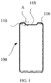
- FIG. 1 is a schematic view of display screen 100 with an irregular shape according to an embodiment.
- FIG. 2 is a partial enlarged view of the portion A in FIG. 1 .
- FIG. 3 is a schematic view of wiring of the connecting lines of the display screen with the irregular shape of FIG. 1 .
- the display screen 100 with the irregular shape includes a substrate (not shown), an irregular-shaped display area 110, a packaging area 120 and a plurality of connecting lines 130.
- the irregular-shaped display area 110, the plurality of connecting lines 130, and the packaging area 120 are all provided on the substrate.
- the irregular-shaped display area 110 includes an irregular-shaped boundary 112 and a pixel area 114, the irregular-shaped boundary 112 is located at a periphery of the pixel area 114.
- the irregular-shaped boundary 112 is a boundary between the pixel area 114 and an outside area.
- a projection of the irregular-shaped boundary 112 on the plane of the irregular-shaped display area 110 may have a circular arc shape or a shape of other curved segments.
- the shape of the irregular-shaped boundary 112 depends on the shape of the irregular-shaped display area 110.
- the pixel area includes a plurality of pixels for displaying. Generally, the plurality of pixel are arranged in rows and columns.
- the packaging area 120 is provided at a periphery of the irregular-shaped boundary 112.
- the packaging area 120 is used to package the irregular display area 110.
- the plurality of connecting lines 130 are located between the irregular-shaped boundary 112 and the packaging area 120.
- the plurality of connecting lines 130 are arranged one by one along the direction from the irregular-shaped boundary 112 to the packaging area 120.
- each of the connecting lines is sequentially connected to a pixel of the pixel area 114.
- the remaining connecting lines are integrally bent towards the irregular-shaped boundary 112, such that the plurality of connecting lines are compactly wired and arranged integrally adjacent to the irregular-shaped boundary.
- the plurality of connecting lines 130 are located between the irregular-shaped boundary 112 and the packaging area 120, and the plurality of connecting lines 130 are arranged one by one along a direction from the irregular-shaped boundary 112 to the packaging area 120. After one connecting line 130 adjacent to the irregular-shaped boundary 112 is connected to the corresponding pixel, the remaining connecting lines 130 are integrally bent towards the irregular-shaped boundary 112, such that the plurality of connecting lines 130 are compactly wired and arranged integrally adjacent to the irregular-shaped boundary 112. On the one hand, the wiring space occupied by the plurality of connecting lines 130 is reduced.
- the connecting lines 130 are integrally arranged more adjacent to the irregular-shaped boundary 112, other lines may also be provided between the packaging area 120 and the plurality of connecting lines 130 while narrowing the frame, so as to facilitate the wiring of other related lines of the display screen 100 with the irregular shape.
- the pixel area of the irregular-shaped display area 110 includes two adjacent protrusion areas 116, and a groove 118 is formed between the two protrusion areas 116.
- a position corresponding to the groove 118 may be used to accommodative an auxiliary device such as a receiver or a camera.
- the irregular-shaped boundary 112 is formed by sides of the protrusion areas 116 adjacent to the groove 118, and the irregular-shaped boundary 112 is arched. That is to say, as observed from a direction perpendicular to the irregular-shaped display area 110, the sides of the protrusion areas 116 adjacent to the groove 118 have arc shapes, and the irregular-shaped boundary 112 is formed by the sides of the arc shapes.
- the pixels of the protrusion areas 116 are arranged in rows and columns. However, since the shapes of the protrusion areas 116 are not regular rectangles, the pixels thereof are not arranged in arrays, that is, the number of pixels in each row is different.
- the display screen 100 with the irregular shape further includes a plurality of compensation loads 140.
- the compensation loads 140 are provided on a side of the protrusion area 116, and the side where the compensation load 140 located is adjacent to the irregular-shaped boundary 112. Tops of two protrusion areas 116 are both provided with the compensation load 140.
- each of the compensation loads 140 is used to compensate the corresponding pixels lacked in the position corresponding to the groove 118, such that the display screen 100 with the irregular shape can still use the driving circuit corresponding to the display screen with regular shape.
- the display screen with regular shape herein means a conventional display screen with a rectangular shape.
- the compensation loads 140 are capacitors. Therefore, for the display screen 100 with the irregular shape, the driving circuit is not required to be redesigned, which reduces the production cost of the display screen 100 with the irregular shape.
- each of the connecting lines is used to connect the compensation loads 140 and the pixels corresponding to the protrusion areas 116. That is, each of the compensation load 140 is connected to pixels in a row corresponding to the protrusion areas 116.
- each of the connecting lines is sequentially connected to a pixel of the pixel area 114. After the connecting line most adjacent to the irregular-shaped boundary 112 is connected to the corresponding pixel, the remaining connecting lines are sequentially bent towards the irregular-shaped boundary 112, such that the plurality of connecting lines 130 are compactly arranged.
- the plurality of connecting lines are arranged along the irregular-shaped boundary 112 from the top of the protrusion area to the bottom of the groove 118.
- the pixels of the row closest to the top of the protrusion area 116 is defined as the first row of pixels 1
- the pixels of the row closest to the bottom of the groove 118 is defined as the last row of pixels
- the rows of pixels between the first row of pixels 1 and the last row of pixels are sequentially ordered.
- the plurality of connecting lines 130 are located one by one between the irregular-shaped boundary 112 and the packaging area 120.
- the connecting line most adjacent to the irregular-shaped boundary 112 is defined as the first connecting line 11, and the connecting line most away from the irregular-shaped boundary 112 is the last connecting line, the connecting lines between the first connecting line 11 and the last connecting line are sequentially ordered.
- the connecting line most adjacent to the irregular-shaped boundary 112 is first connected to the pixels of the protrusion area 116. In other words, the first connecting line 11 is first connected to the first row of pixels 1. Thereafter, the remaining connecting lines are integrally bent towards the irregular-shaped boundary 112, that is, the remaining connecting lines are as close as possible to the irregular-shaped boundary 112. As shown in FIG.
- the remaining connecting lines are integrally bent towards the irregular-shaped boundary 112 and form a first bending area 33.
- the second connecting line 22 is connected to a second row of pixels 2 of the protrusion area 116, the remaining connecting lines are bent as close as possible to the irregular-shaped boundary 112.
- the remaining connecting lines are similarly arranged.
- the connecting lines 130 are compactly arranged, so as to save the space.
- the distance between the packaging area 120 and the irregular-shaped boundary 112 is constant, according to the conventional wiring manner, the distance between the plurality of connecting lines 130 and the packaging area 120 is only 154 ⁇ m. While for the same display screen 100 with the irregular shape, if the plurality of connecting lines 130 are arranged based on the wiring method of the present disclosure, the distance between the plurality of connecting lines 130 and the packaging area 120 can be 279 ⁇ m. This fully demonstrates that in the display screen 100 with the irregular shape of the present embodiment, the plurality of connecting lines 130 occupy a less space.
- the distance between the packaging area 120 and the irregular-shaped boundary 112 can be reduced within an allowable range, that is, the frame of the irregular-shaped display area can be made narrower.
- other lines may be provided between the packaging area 120 and the plurality of connecting lines 130 while making the frame of irregular-shaped display area narrower.
- the display screen 100 with the irregular shape further includes a cathode power line.
- the cathode power line is provided on a cathode wiring area 150 of the substrate, and the cathode wiring area 150 is provided between the packaging area 120 and the plurality of connecting lines.
- the cathode power line can have sufficient wiring space between the plurality of connecting lines 130 and the packaging area 120. Since the cathode power line can be provided between the plurality of connecting lines 130 and the packaging area 120, the cathode power line is easy to be arranged.
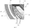
- FIG. 4 is a schematic view of a display screen with an irregular shape according to another embodiment.
- the irregular-shaped display area includes a sector display area 210, and the irregular-shaped boundary 212 is an arc boundary of the sector display area 210.
- the pixels of the sector display area 210 are also arranged in rows and columns.
- the display screen 200 with an irregular shape further includes a plurality of data signal units 241 provided between the irregular-shaped boundary 212 and the package area 220.
- the plurality of data signal units 241 form a scanning circuit of the display screen 200 with the irregular shape.
- the connecting lines include data lines 232.
- the plurality of data lines 232 are located between the data signal units 241 and the packaging area 220.
- Each of the data signal units 241 is connected to the corresponding pixel of the sector display area 210 via the corresponding data line 232.
- the remaining data lines 232 are integrally bent towards the irregular-shaped boundary 212, such that the plurality of data lines 232 are compactly wired and arranged integrally adjacent to the irregular-shaped boundary 212, thereby saving the space.
- the data signal units 241 are sorted from bottom to top, the bottommost one is the first data signal unit 241, the topmost one is the last data signal unit 241, and the data signal units 241 between the first data signal unit 241 and the last data signal unit 241 are sequentially ordered.
- the data line 232 most adjacent to the first data signal unit 241 is the first data line 232.
- the data line 232 furthest away from the first data line 232 is the last data line 232, the data lines 232 between the first data line 232 and the last data line 232 are sequentially ordered.
- the data lines 232 are arranged from bottom to top.
- the first data line 232 is connected to the first data signal unit 241 and the corresponding pixels of the sector display area 210.
- the remaining data lines 232 and the corresponding data signal units 241 are connected in similar manners.
- the second data line 232 is connected to the second data signal unit 241.
- the remaining data lines 232 are integrally bent towards the irregular-shaped boundary 212.
- the second data line 232 is connected to the second data signal unit 241
- the remaining data lines 232 are integrally bent towards the irregular-shaped boundary 212.
- Remaining data lines 232 are bent similarly, until the last data line 232 is connected to the last data signal unit 241. In this way, all the data lines 232 are compactly arranged, thereby saving the space.
- the display screen 200 with the irregular shape further includes a plurality of driving circuit units 243.
- the connecting lines further include a plurality of scan lines 234.
- the plurality of driving circuit units 243 are provided between the plurality of data lines 232 and the packaging area 220.
- the plurality of driving circuit units 243 form a driving circuit of the display screen 200 with the irregular shape.
- the plurality of scan lines 234 are located between the plurality of data lines 232 and the driving circuit units 243.
- Each of the driving circuit units 243 is connected to the pixel of the sector display area 210 via the corresponding scan line 234.
- the remaining scan lines 234 are integrally bent towards the packaging area 220, such that the plurality of scan lines 234 are compactly wired and arranged integrally adjacent to the packaging area 220, thereby saving the space.
- the driving circuit units 243 are sorted from top to bottom, the topmost one is the first driving circuit unit 243, the bottommost one is the last driving circuit unit 243, and the driving circuit units 243 between the first driving circuit unit 243 and the last driving circuit unit 243 are sequentially ordered.
- the scan line 234 most adjacent to the first driving circuit unit 243 is the first scan line 234.
- the scan line 234 furthest away from the first scan line 234 is the last scan line 234, the scan lines 234 between the first scan line 234 and the last scan line 234 are sequentially ordered.
- the scan lines 234 are arranged from top to bottom.
- the first scan line 234 is connected to the first driving circuit unit 243 and the corresponding pixels of the sector display area 210.
- the remaining scan lines 234 are connected in similar manners.
- the second scan line 234 is connected the second driving circuit unit 243.
- the remaining scan lines 234 are integrally bent towards the packaging area 220. That is, the remaining scan lines are sequentially bent towards the driving circuit units 243.
- the second scan line 234 is connected the second driving circuit unit 243
- the remaining scan lines 234 are integrally bent towards the packaging area 220.
- the remaining scan lines 234 are bent similarly, until the last scan line 234 is connected to the last driving circuit unit 243. In this way, all the scan lines 234 are compactly arranged, thereby saving the space.
- the wiring of the plurality of scan lines 234 and the plurality of data lines 232 allows the scan lines 234 and the data lines 232 to save space, respectively.
- the plurality of scan lines 234 are more adjacent to the driving circuit units 243, and the plurality of data lines 232 are more adjacent to the data signal units 241, thereby increasing the gap between the plurality of scan lines 234 and the plurality of data lines 232. Therefore, during designing the scan lines 234 and the data lines 232, the plurality of scan lines 234 and the plurality of data lines 232 can be more adjacent to each other, thereby decreasing the overall space occupied by the scan lines 234 and the data lines 232. In this way, the scanning circuit and the driving circuit can be integrally more adjacent to the sector display area 210, such that the space between the driving circuit and the packaging area 220 is increased.
- the distance from the packaging area 220 to the irregular-shaped boundary 212 can be reduced within an allowable range, thereby narrowing the frame of the display screen 200 with the irregular shape.
- other lines may also be provided between the packaging area 220 and the driving circuit.
- a cathode wiring area 250 can be provided between the driving circuit and the packaging area 220, cathode power line can be provided on the cathode wiring area 250, such that the cathode power line can be easily arranged.
- the compensation load, data signal unit 241, and the driving circuit unit 243 are only used as examples to illustrate the wiring structure of the plurality of connecting lines 230.
- the wiring structure of the plurality of connecting lines 230 can be applied in circuits of any display screens 200 with irregular shapes.
- the present disclosure further provides a display device including the display screen with the irregular shape of any one of the aforementioned embodiments. In this way, the frame of the display screen of the display device can be narrower.
Landscapes
- Engineering & Computer Science (AREA)
- Physics & Mathematics (AREA)
- Theoretical Computer Science (AREA)
- General Physics & Mathematics (AREA)
- Computer Hardware Design (AREA)
- General Engineering & Computer Science (AREA)
- Nonlinear Science (AREA)
- Human Computer Interaction (AREA)
- Devices For Indicating Variable Information By Combining Individual Elements (AREA)
- Chemical & Material Sciences (AREA)
- Crystallography & Structural Chemistry (AREA)
- Mathematical Physics (AREA)
- Optics & Photonics (AREA)
- Electroluminescent Light Sources (AREA)
- Liquid Crystal (AREA)
Applications Claiming Priority (2)
| Application Number | Priority Date | Filing Date | Title |
|---|---|---|---|
| CN201810455765.2A CN108389516B (zh) | 2018-05-14 | 2018-05-14 | 异形显示屏及显示装置 |
| PCT/CN2018/104639 WO2019218544A1 (fr) | 2018-05-14 | 2018-09-07 | Écran d'affichage de forme spéciale et appareil d'affichage |
Publications (3)
| Publication Number | Publication Date |
|---|---|
| EP3627480A1 true EP3627480A1 (fr) | 2020-03-25 |
| EP3627480A4 EP3627480A4 (fr) | 2020-07-01 |
| EP3627480B1 EP3627480B1 (fr) | 2022-05-11 |
Family
ID=63071589
Family Applications (1)
| Application Number | Title | Priority Date | Filing Date |
|---|---|---|---|
| EP18918409.6A Active EP3627480B1 (fr) | 2018-05-14 | 2018-09-07 | Écran d'affichage de forme spéciale et appareil d'affichage |
Country Status (7)
| Country | Link |
|---|---|
| US (1) | US11269381B2 (fr) |
| EP (1) | EP3627480B1 (fr) |
| JP (1) | JP7061625B2 (fr) |
| KR (1) | KR102269359B1 (fr) |
| CN (1) | CN108389516B (fr) |
| TW (1) | TWI700677B (fr) |
| WO (1) | WO2019218544A1 (fr) |
Cited By (1)
| Publication number | Priority date | Publication date | Assignee | Title |
|---|---|---|---|---|
| US11100868B2 (en) | 2018-10-26 | 2021-08-24 | Kunshan Go-Visionox Opto-Electronics Co., Ltd. | Display devices, display panels and capacitance compensation method thereof |
Families Citing this family (12)
| Publication number | Priority date | Publication date | Assignee | Title |
|---|---|---|---|---|
| CN108389516B (zh) * | 2018-05-14 | 2021-06-29 | 昆山国显光电有限公司 | 异形显示屏及显示装置 |
| CN109192137B (zh) * | 2018-10-30 | 2021-06-29 | 昆山国显光电有限公司 | 显示器及其显示面板 |
| CN110299075B (zh) * | 2019-04-30 | 2021-06-04 | 厦门天马微电子有限公司 | 显示面板及显示装置 |
| CN111489648B (zh) * | 2020-05-08 | 2022-02-11 | 友达光电(昆山)有限公司 | 显示面板、显示装置及其制作方法 |
| KR20220030467A (ko) | 2020-09-01 | 2022-03-11 | 삼성디스플레이 주식회사 | 디스플레이 패널 및 디스플레이 장치 |
| CN114531922B (zh) | 2020-09-22 | 2025-08-12 | 京东方科技集团股份有限公司 | 显示基板及显示装置 |
| US12356810B2 (en) | 2020-10-23 | 2025-07-08 | Chengdu Boe Optoelectronics Technology Co., Ltd. | Display substrate with stepped wire configuration, dummy rectangle units and display apparatus, and manufacturing method thereof |
| CN113554969B (zh) * | 2021-07-16 | 2024-04-12 | 武汉天马微电子有限公司 | 显示面板及显示装置 |
| CN113763815A (zh) * | 2021-09-03 | 2021-12-07 | 深圳市华星光电半导体显示技术有限公司 | 显示面板及其制备方法 |
| WO2024020855A1 (fr) | 2022-07-27 | 2024-02-01 | 京东方科技集团股份有限公司 | Carte de circuit imprimé (pcb), dispositif d'affichage comprenant une pcb, et système d'affichage d'image |
| WO2024138319A1 (fr) * | 2022-12-26 | 2024-07-04 | 京东方科技集团股份有限公司 | Panneau d'affichage et dispositif d'affichage |
| WO2025076638A1 (fr) * | 2023-10-08 | 2025-04-17 | 京东方科技集团股份有限公司 | Substrat de réseau et sa carte mère, dispositif d'affichage et véhicule |
Family Cites Families (28)
| Publication number | Priority date | Publication date | Assignee | Title |
|---|---|---|---|---|
| US5270693A (en) * | 1991-08-19 | 1993-12-14 | Smiths Industries, Inc. | Enlarged area addressable matrix |
| GB0412782D0 (en) * | 2004-06-09 | 2004-07-14 | Koninkl Philips Electronics Nv | Non-rectangular display device |
| US8023087B2 (en) * | 2006-08-23 | 2011-09-20 | Hitachi Displays, Ltd. | Display device having particular pixels and signal wiring internal circuits |
| US8638280B2 (en) * | 2007-04-27 | 2014-01-28 | Nlt Technologies, Ltd. | Non-rectangular display apparatus |
| KR101535929B1 (ko) * | 2008-12-02 | 2015-07-10 | 삼성디스플레이 주식회사 | 표시기판, 이를 갖는 표시패널 및 이를 갖는 표시장치 |
| US9514673B2 (en) | 2012-11-22 | 2016-12-06 | Lg Display Co., Ltd. | Organic light emitting display device |
| CN103424901A (zh) * | 2013-08-19 | 2013-12-04 | 京东方科技集团股份有限公司 | 一种显示面板及显示模组 |
| TWI504969B (zh) * | 2014-10-27 | 2015-10-21 | Au Optronics Corp | 顯示面板以及顯示裝置 |
| KR102239481B1 (ko) * | 2014-12-31 | 2021-04-13 | 엘지디스플레이 주식회사 | 디스플레이 장치 |
| JP6533065B2 (ja) * | 2015-02-12 | 2019-06-19 | 株式会社ジャパンディスプレイ | 表示装置 |
| JP2016148775A (ja) * | 2015-02-12 | 2016-08-18 | 株式会社ジャパンディスプレイ | 表示装置 |
| JP6536187B2 (ja) | 2015-06-05 | 2019-07-03 | 三菱電機株式会社 | アレイ基板及び当該アレイ基板を備えた液晶表示装置 |
| WO2017043429A1 (fr) | 2015-09-11 | 2017-03-16 | シャープ株式会社 | Dispositif d'affichage et organe de circuit |
| CN109903709A (zh) * | 2016-01-21 | 2019-06-18 | 苹果公司 | 有机发光二极管显示器的电源和数据路由结构 |
| JP2017134338A (ja) * | 2016-01-29 | 2017-08-03 | 株式会社ジャパンディスプレイ | 表示装置 |
| JP6689088B2 (ja) * | 2016-02-08 | 2020-04-28 | 株式会社ジャパンディスプレイ | 表示装置 |
| SG11201807505SA (en) * | 2016-03-28 | 2018-09-27 | Apple Inc | Light-emitting diode displays |
| KR102666848B1 (ko) * | 2016-05-17 | 2024-05-21 | 삼성디스플레이 주식회사 | 표시 장치 |
| TWI709791B (zh) * | 2016-07-07 | 2020-11-11 | 日商半導體能源研究所股份有限公司 | 顯示裝置及電子裝置 |
| JP6773277B2 (ja) * | 2016-08-05 | 2020-10-21 | 天馬微電子有限公司 | 表示装置 |
| KR102690366B1 (ko) * | 2016-09-12 | 2024-08-02 | 삼성디스플레이 주식회사 | 표시 장치 |
| US10360854B2 (en) * | 2017-06-14 | 2019-07-23 | Lg Display Co., Ltd. | Gate driving circuit having a compensating auxiliary load and display device using the same |
| CN107342036B (zh) * | 2017-08-21 | 2020-10-30 | 厦门天马微电子有限公司 | 显示面板及显示装置 |
| CN107561799B (zh) * | 2017-08-25 | 2021-07-20 | 厦门天马微电子有限公司 | 一种阵列基板、显示面板及显示装置 |
| CN107481669A (zh) * | 2017-09-08 | 2017-12-15 | 武汉天马微电子有限公司 | 一种显示面板及显示装置 |
| CN107611142B (zh) * | 2017-09-11 | 2020-06-09 | 上海天马有机发光显示技术有限公司 | 显示面板及显示装置 |
| CN108389516B (zh) | 2018-05-14 | 2021-06-29 | 昆山国显光电有限公司 | 异形显示屏及显示装置 |
| CN208271481U (zh) * | 2018-05-14 | 2018-12-21 | 昆山国显光电有限公司 | 异形显示屏及显示装置 |
-
2018
- 2018-05-14 CN CN201810455765.2A patent/CN108389516B/zh active Active
- 2018-09-07 WO PCT/CN2018/104639 patent/WO2019218544A1/fr not_active Ceased
- 2018-09-07 US US16/326,911 patent/US11269381B2/en active Active
- 2018-09-07 EP EP18918409.6A patent/EP3627480B1/fr active Active
- 2018-09-07 JP JP2019564854A patent/JP7061625B2/ja active Active
- 2018-09-07 KR KR1020197034705A patent/KR102269359B1/ko active Active
- 2018-10-09 TW TW107135645A patent/TWI700677B/zh active
Cited By (1)
| Publication number | Priority date | Publication date | Assignee | Title |
|---|---|---|---|---|
| US11100868B2 (en) | 2018-10-26 | 2021-08-24 | Kunshan Go-Visionox Opto-Electronics Co., Ltd. | Display devices, display panels and capacitance compensation method thereof |
Also Published As
| Publication number | Publication date |
|---|---|
| KR102269359B1 (ko) | 2021-06-25 |
| JP7061625B2 (ja) | 2022-04-28 |
| EP3627480B1 (fr) | 2022-05-11 |
| WO2019218544A1 (fr) | 2019-11-21 |
| TW201903736A (zh) | 2019-01-16 |
| TWI700677B (zh) | 2020-08-01 |
| CN108389516A (zh) | 2018-08-10 |
| EP3627480A4 (fr) | 2020-07-01 |
| JP2020522734A (ja) | 2020-07-30 |
| CN108389516B (zh) | 2021-06-29 |
| US11269381B2 (en) | 2022-03-08 |
| KR20190138690A (ko) | 2019-12-13 |
| US20210349500A1 (en) | 2021-11-11 |
Similar Documents
| Publication | Publication Date | Title |
|---|---|---|
| EP3627480A1 (fr) | Écran d'affichage de forme spéciale et appareil d'affichage | |
| US10854124B2 (en) | Display panel and display device including the same | |
| US11968870B2 (en) | Display panel and display device | |
| US11424297B2 (en) | Display panel having multiple display regions and display apparatus | |
| US8023087B2 (en) | Display device having particular pixels and signal wiring internal circuits | |
| US11195448B2 (en) | Display and mobile terminal | |
| CN108648615A (zh) | 显示面板 | |
| CN112102727B (zh) | 显示面板和显示装置 | |
| CN111091776B (zh) | 驱动电路及显示面板 | |
| US20210295755A1 (en) | Display device | |
| CN108803178B (zh) | 液晶显示面板 | |
| US10790312B2 (en) | Display panel and display device | |
| US10614735B2 (en) | Flexible GOA display panel and method of manufacturing the same | |
| TWI407348B (zh) | 接觸墊陣列 | |
| US20230280806A1 (en) | Display panel and display terminal | |
| US20190287445A1 (en) | Array substrate and display panel | |
| JP2008309825A (ja) | 液晶表示装置 | |
| CN113327536B (zh) | 显示面板和显示设备 | |
| US11257879B2 (en) | Display panels and display devices thereof | |
| CN112258983A (zh) | 一种显示面板和显示装置 | |
| US11631356B2 (en) | Display panel and display device | |
| KR20150060009A (ko) | 표시장치 및 표시패널 | |
| US20240387777A1 (en) | Display panels and display devices | |
| US20240282250A1 (en) | Display panel and display apparatus | |
| US20260090164A1 (en) | Light-emitting master plate, light-emitting panel, and cutting method for light-emitting master plate |
Legal Events
| Date | Code | Title | Description |
|---|---|---|---|
| STAA | Information on the status of an ep patent application or granted ep patent |
Free format text: STATUS: UNKNOWN |
|
| STAA | Information on the status of an ep patent application or granted ep patent |
Free format text: STATUS: THE INTERNATIONAL PUBLICATION HAS BEEN MADE |
|
| PUAI | Public reference made under article 153(3) epc to a published international application that has entered the european phase |
Free format text: ORIGINAL CODE: 0009012 |
|
| STAA | Information on the status of an ep patent application or granted ep patent |
Free format text: STATUS: REQUEST FOR EXAMINATION WAS MADE |
|
| 17P | Request for examination filed |
Effective date: 20191120 |
|
| AK | Designated contracting states |
Kind code of ref document: A1 Designated state(s): AL AT BE BG CH CY CZ DE DK EE ES FI FR GB GR HR HU IE IS IT LI LT LU LV MC MK MT NL NO PL PT RO RS SE SI SK SM TR |
|
| AX | Request for extension of the european patent |
Extension state: BA ME |
|
| A4 | Supplementary search report drawn up and despatched |
Effective date: 20200602 |
|
| RIC1 | Information provided on ipc code assigned before grant |
Ipc: G02F 1/1345 20060101ALI20200526BHEP Ipc: G09F 9/30 20060101AFI20200526BHEP Ipc: G09G 3/20 20060101ALI20200526BHEP |
|
| DAV | Request for validation of the european patent (deleted) | ||
| DAX | Request for extension of the european patent (deleted) | ||
| GRAP | Despatch of communication of intention to grant a patent |
Free format text: ORIGINAL CODE: EPIDOSNIGR1 |
|
| STAA | Information on the status of an ep patent application or granted ep patent |
Free format text: STATUS: GRANT OF PATENT IS INTENDED |
|
| GRAS | Grant fee paid |
Free format text: ORIGINAL CODE: EPIDOSNIGR3 |
|
| GRAA | (expected) grant |
Free format text: ORIGINAL CODE: 0009210 |
|
| STAA | Information on the status of an ep patent application or granted ep patent |
Free format text: STATUS: THE PATENT HAS BEEN GRANTED |
|
| INTG | Intention to grant announced |
Effective date: 20220317 |
|
| AK | Designated contracting states |
Kind code of ref document: B1 Designated state(s): AL AT BE BG CH CY CZ DE DK EE ES FI FR GB GR HR HU IE IS IT LI LT LU LV MC MK MT NL NO PL PT RO RS SE SI SK SM TR |
|
| REG | Reference to a national code |
Ref country code: GB Ref legal event code: FG4D |
|
| REG | Reference to a national code |
Ref country code: CH Ref legal event code: EP |
|
| REG | Reference to a national code |
Ref country code: AT Ref legal event code: REF Ref document number: 1492126 Country of ref document: AT Kind code of ref document: T Effective date: 20220515 |
|
| REG | Reference to a national code |
Ref country code: DE Ref legal event code: R096 Ref document number: 602018035636 Country of ref document: DE |
|
| REG | Reference to a national code |
Ref country code: IE Ref legal event code: FG4D |
|
| REG | Reference to a national code |
Ref country code: LT Ref legal event code: MG9D |
|
| REG | Reference to a national code |
Ref country code: NL Ref legal event code: MP Effective date: 20220511 |
|
| REG | Reference to a national code |
Ref country code: AT Ref legal event code: MK05 Ref document number: 1492126 Country of ref document: AT Kind code of ref document: T Effective date: 20220511 |
|
| PG25 | Lapsed in a contracting state [announced via postgrant information from national office to epo] |
Ref country code: SE Free format text: LAPSE BECAUSE OF FAILURE TO SUBMIT A TRANSLATION OF THE DESCRIPTION OR TO PAY THE FEE WITHIN THE PRESCRIBED TIME-LIMIT Effective date: 20220511 Ref country code: PT Free format text: LAPSE BECAUSE OF FAILURE TO SUBMIT A TRANSLATION OF THE DESCRIPTION OR TO PAY THE FEE WITHIN THE PRESCRIBED TIME-LIMIT Effective date: 20220912 Ref country code: NO Free format text: LAPSE BECAUSE OF FAILURE TO SUBMIT A TRANSLATION OF THE DESCRIPTION OR TO PAY THE FEE WITHIN THE PRESCRIBED TIME-LIMIT Effective date: 20220811 Ref country code: NL Free format text: LAPSE BECAUSE OF FAILURE TO SUBMIT A TRANSLATION OF THE DESCRIPTION OR TO PAY THE FEE WITHIN THE PRESCRIBED TIME-LIMIT Effective date: 20220511 Ref country code: LT Free format text: LAPSE BECAUSE OF FAILURE TO SUBMIT A TRANSLATION OF THE DESCRIPTION OR TO PAY THE FEE WITHIN THE PRESCRIBED TIME-LIMIT Effective date: 20220511 Ref country code: HR Free format text: LAPSE BECAUSE OF FAILURE TO SUBMIT A TRANSLATION OF THE DESCRIPTION OR TO PAY THE FEE WITHIN THE PRESCRIBED TIME-LIMIT Effective date: 20220511 Ref country code: GR Free format text: LAPSE BECAUSE OF FAILURE TO SUBMIT A TRANSLATION OF THE DESCRIPTION OR TO PAY THE FEE WITHIN THE PRESCRIBED TIME-LIMIT Effective date: 20220812 Ref country code: FI Free format text: LAPSE BECAUSE OF FAILURE TO SUBMIT A TRANSLATION OF THE DESCRIPTION OR TO PAY THE FEE WITHIN THE PRESCRIBED TIME-LIMIT Effective date: 20220511 Ref country code: ES Free format text: LAPSE BECAUSE OF FAILURE TO SUBMIT A TRANSLATION OF THE DESCRIPTION OR TO PAY THE FEE WITHIN THE PRESCRIBED TIME-LIMIT Effective date: 20220511 Ref country code: BG Free format text: LAPSE BECAUSE OF FAILURE TO SUBMIT A TRANSLATION OF THE DESCRIPTION OR TO PAY THE FEE WITHIN THE PRESCRIBED TIME-LIMIT Effective date: 20220811 Ref country code: AT Free format text: LAPSE BECAUSE OF FAILURE TO SUBMIT A TRANSLATION OF THE DESCRIPTION OR TO PAY THE FEE WITHIN THE PRESCRIBED TIME-LIMIT Effective date: 20220511 |
|
| PG25 | Lapsed in a contracting state [announced via postgrant information from national office to epo] |
Ref country code: RS Free format text: LAPSE BECAUSE OF FAILURE TO SUBMIT A TRANSLATION OF THE DESCRIPTION OR TO PAY THE FEE WITHIN THE PRESCRIBED TIME-LIMIT Effective date: 20220511 Ref country code: PL Free format text: LAPSE BECAUSE OF FAILURE TO SUBMIT A TRANSLATION OF THE DESCRIPTION OR TO PAY THE FEE WITHIN THE PRESCRIBED TIME-LIMIT Effective date: 20220511 Ref country code: LV Free format text: LAPSE BECAUSE OF FAILURE TO SUBMIT A TRANSLATION OF THE DESCRIPTION OR TO PAY THE FEE WITHIN THE PRESCRIBED TIME-LIMIT Effective date: 20220511 Ref country code: IS Free format text: LAPSE BECAUSE OF FAILURE TO SUBMIT A TRANSLATION OF THE DESCRIPTION OR TO PAY THE FEE WITHIN THE PRESCRIBED TIME-LIMIT Effective date: 20220911 |
|
| PG25 | Lapsed in a contracting state [announced via postgrant information from national office to epo] |
Ref country code: SM Free format text: LAPSE BECAUSE OF FAILURE TO SUBMIT A TRANSLATION OF THE DESCRIPTION OR TO PAY THE FEE WITHIN THE PRESCRIBED TIME-LIMIT Effective date: 20220511 Ref country code: SK Free format text: LAPSE BECAUSE OF FAILURE TO SUBMIT A TRANSLATION OF THE DESCRIPTION OR TO PAY THE FEE WITHIN THE PRESCRIBED TIME-LIMIT Effective date: 20220511 Ref country code: RO Free format text: LAPSE BECAUSE OF FAILURE TO SUBMIT A TRANSLATION OF THE DESCRIPTION OR TO PAY THE FEE WITHIN THE PRESCRIBED TIME-LIMIT Effective date: 20220511 Ref country code: EE Free format text: LAPSE BECAUSE OF FAILURE TO SUBMIT A TRANSLATION OF THE DESCRIPTION OR TO PAY THE FEE WITHIN THE PRESCRIBED TIME-LIMIT Effective date: 20220511 Ref country code: DK Free format text: LAPSE BECAUSE OF FAILURE TO SUBMIT A TRANSLATION OF THE DESCRIPTION OR TO PAY THE FEE WITHIN THE PRESCRIBED TIME-LIMIT Effective date: 20220511 Ref country code: CZ Free format text: LAPSE BECAUSE OF FAILURE TO SUBMIT A TRANSLATION OF THE DESCRIPTION OR TO PAY THE FEE WITHIN THE PRESCRIBED TIME-LIMIT Effective date: 20220511 |
|
| REG | Reference to a national code |
Ref country code: DE Ref legal event code: R097 Ref document number: 602018035636 Country of ref document: DE |
|
| PLBE | No opposition filed within time limit |
Free format text: ORIGINAL CODE: 0009261 |
|
| STAA | Information on the status of an ep patent application or granted ep patent |
Free format text: STATUS: NO OPPOSITION FILED WITHIN TIME LIMIT |
|
| PG25 | Lapsed in a contracting state [announced via postgrant information from national office to epo] |
Ref country code: AL Free format text: LAPSE BECAUSE OF FAILURE TO SUBMIT A TRANSLATION OF THE DESCRIPTION OR TO PAY THE FEE WITHIN THE PRESCRIBED TIME-LIMIT Effective date: 20220511 |
|
| 26N | No opposition filed |
Effective date: 20230214 |
|
| PG25 | Lapsed in a contracting state [announced via postgrant information from national office to epo] |
Ref country code: MC Free format text: LAPSE BECAUSE OF FAILURE TO SUBMIT A TRANSLATION OF THE DESCRIPTION OR TO PAY THE FEE WITHIN THE PRESCRIBED TIME-LIMIT Effective date: 20220511 |
|
| REG | Reference to a national code |
Ref country code: CH Ref legal event code: PL |
|
| REG | Reference to a national code |
Ref country code: BE Ref legal event code: MM Effective date: 20220930 |
|
| PG25 | Lapsed in a contracting state [announced via postgrant information from national office to epo] |
Ref country code: SI Free format text: LAPSE BECAUSE OF FAILURE TO SUBMIT A TRANSLATION OF THE DESCRIPTION OR TO PAY THE FEE WITHIN THE PRESCRIBED TIME-LIMIT Effective date: 20220511 |
|
| PG25 | Lapsed in a contracting state [announced via postgrant information from national office to epo] |
Ref country code: LU Free format text: LAPSE BECAUSE OF NON-PAYMENT OF DUE FEES Effective date: 20220907 |
|
| P01 | Opt-out of the competence of the unified patent court (upc) registered |
Effective date: 20230526 |
|
| PG25 | Lapsed in a contracting state [announced via postgrant information from national office to epo] |
Ref country code: LI Free format text: LAPSE BECAUSE OF NON-PAYMENT OF DUE FEES Effective date: 20220930 Ref country code: IE Free format text: LAPSE BECAUSE OF NON-PAYMENT OF DUE FEES Effective date: 20220907 Ref country code: CH Free format text: LAPSE BECAUSE OF NON-PAYMENT OF DUE FEES Effective date: 20220930 |
|
| PG25 | Lapsed in a contracting state [announced via postgrant information from national office to epo] |
Ref country code: BE Free format text: LAPSE BECAUSE OF NON-PAYMENT OF DUE FEES Effective date: 20220930 |
|
| PG25 | Lapsed in a contracting state [announced via postgrant information from national office to epo] |
Ref country code: IT Free format text: LAPSE BECAUSE OF FAILURE TO SUBMIT A TRANSLATION OF THE DESCRIPTION OR TO PAY THE FEE WITHIN THE PRESCRIBED TIME-LIMIT Effective date: 20220511 |
|
| PG25 | Lapsed in a contracting state [announced via postgrant information from national office to epo] |
Ref country code: HU Free format text: LAPSE BECAUSE OF FAILURE TO SUBMIT A TRANSLATION OF THE DESCRIPTION OR TO PAY THE FEE WITHIN THE PRESCRIBED TIME-LIMIT; INVALID AB INITIO Effective date: 20180907 |
|
| PG25 | Lapsed in a contracting state [announced via postgrant information from national office to epo] |
Ref country code: CY Free format text: LAPSE BECAUSE OF FAILURE TO SUBMIT A TRANSLATION OF THE DESCRIPTION OR TO PAY THE FEE WITHIN THE PRESCRIBED TIME-LIMIT Effective date: 20220511 |
|
| PG25 | Lapsed in a contracting state [announced via postgrant information from national office to epo] |
Ref country code: MK Free format text: LAPSE BECAUSE OF FAILURE TO SUBMIT A TRANSLATION OF THE DESCRIPTION OR TO PAY THE FEE WITHIN THE PRESCRIBED TIME-LIMIT Effective date: 20220511 |
|
| PG25 | Lapsed in a contracting state [announced via postgrant information from national office to epo] |
Ref country code: TR Free format text: LAPSE BECAUSE OF FAILURE TO SUBMIT A TRANSLATION OF THE DESCRIPTION OR TO PAY THE FEE WITHIN THE PRESCRIBED TIME-LIMIT Effective date: 20220511 |
|
| PG25 | Lapsed in a contracting state [announced via postgrant information from national office to epo] |
Ref country code: MT Free format text: LAPSE BECAUSE OF FAILURE TO SUBMIT A TRANSLATION OF THE DESCRIPTION OR TO PAY THE FEE WITHIN THE PRESCRIBED TIME-LIMIT Effective date: 20220511 |
|
| PG25 | Lapsed in a contracting state [announced via postgrant information from national office to epo] |
Ref country code: BG Free format text: LAPSE BECAUSE OF FAILURE TO SUBMIT A TRANSLATION OF THE DESCRIPTION OR TO PAY THE FEE WITHIN THE PRESCRIBED TIME-LIMIT Effective date: 20220511 |
|
| PG25 | Lapsed in a contracting state [announced via postgrant information from national office to epo] |
Ref country code: BG Free format text: LAPSE BECAUSE OF FAILURE TO SUBMIT A TRANSLATION OF THE DESCRIPTION OR TO PAY THE FEE WITHIN THE PRESCRIBED TIME-LIMIT Effective date: 20220511 |
|
| PGFP | Annual fee paid to national office [announced via postgrant information from national office to epo] |
Ref country code: DE Payment date: 20250916 Year of fee payment: 8 |
|
| PGFP | Annual fee paid to national office [announced via postgrant information from national office to epo] |
Ref country code: GB Payment date: 20250919 Year of fee payment: 8 |
|
| PGFP | Annual fee paid to national office [announced via postgrant information from national office to epo] |
Ref country code: FR Payment date: 20250929 Year of fee payment: 8 |
|
| REG | Reference to a national code |
Ref country code: GB Ref legal event code: 732E Free format text: REGISTERED BETWEEN 20251218 AND 20251224 |
|
| REG | Reference to a national code |
Ref country code: DE Ref legal event code: R081 Ref document number: 602018035636 Country of ref document: DE Owner name: SUZHOU GOVISIONOX INNOVATION TECHNOLOGY CO., L, CN Free format text: FORMER OWNER: KUNSHAN GO-VISIONOX OPTO-ELECTRONICS CO., LTD., KUNSHAN CITY, JIANGSU, CN |