EP3627558B1 - Doppelseitiger kondensator und herstellungsverfahren dafür - Google Patents
Doppelseitiger kondensator und herstellungsverfahren dafür Download PDFInfo
- Publication number
- EP3627558B1 EP3627558B1 EP18914929.7A EP18914929A EP3627558B1 EP 3627558 B1 EP3627558 B1 EP 3627558B1 EP 18914929 A EP18914929 A EP 18914929A EP 3627558 B1 EP3627558 B1 EP 3627558B1
- Authority
- EP
- European Patent Office
- Prior art keywords
- trench
- layer
- semiconductor layer
- insulating layer
- passivation
- Prior art date
- Legal status (The legal status is an assumption and is not a legal conclusion. Google has not performed a legal analysis and makes no representation as to the accuracy of the status listed.)
- Active
Links
Images

Classifications
-
- H—ELECTRICITY
- H10—SEMICONDUCTOR DEVICES; ELECTRIC SOLID-STATE DEVICES NOT OTHERWISE PROVIDED FOR
- H10D—INORGANIC ELECTRIC SEMICONDUCTOR DEVICES
- H10D1/00—Resistors, capacitors or inductors
- H10D1/01—Manufacture or treatment
- H10D1/041—Manufacture or treatment of capacitors having no potential barriers
- H10D1/043—Manufacture or treatment of capacitors having no potential barriers using patterning processes to form electrode extensions, e.g. etching
-
- H—ELECTRICITY
- H10—SEMICONDUCTOR DEVICES; ELECTRIC SOLID-STATE DEVICES NOT OTHERWISE PROVIDED FOR
- H10D—INORGANIC ELECTRIC SEMICONDUCTOR DEVICES
- H10D1/00—Resistors, capacitors or inductors
- H10D1/60—Capacitors
- H10D1/68—Capacitors having no potential barriers
- H10D1/692—Electrodes
- H10D1/711—Electrodes having non-planar surfaces, e.g. formed by texturisation
- H10D1/716—Electrodes having non-planar surfaces, e.g. formed by texturisation having vertical extensions
-
- H—ELECTRICITY
- H10—SEMICONDUCTOR DEVICES; ELECTRIC SOLID-STATE DEVICES NOT OTHERWISE PROVIDED FOR
- H10D—INORGANIC ELECTRIC SEMICONDUCTOR DEVICES
- H10D1/00—Resistors, capacitors or inductors
- H10D1/60—Capacitors
- H10D1/62—Capacitors having potential barriers
- H10D1/66—Conductor-insulator-semiconductor capacitors, e.g. MOS capacitors
- H10D1/665—Trench conductor-insulator-semiconductor capacitors, e.g. trench MOS capacitors
-
- H—ELECTRICITY
- H10—SEMICONDUCTOR DEVICES; ELECTRIC SOLID-STATE DEVICES NOT OTHERWISE PROVIDED FOR
- H10D—INORGANIC ELECTRIC SEMICONDUCTOR DEVICES
- H10D84/00—Integrated devices formed in or on semiconductor substrates that comprise only semiconducting layers, e.g. on Si wafers or on GaAs-on-Si wafers
- H10D84/201—Integrated devices formed in or on semiconductor substrates that comprise only semiconducting layers, e.g. on Si wafers or on GaAs-on-Si wafers characterised by the integration of only components covered by H10D1/00 or H10D8/00, e.g. RLC circuits
- H10D84/204—Integrated devices formed in or on semiconductor substrates that comprise only semiconducting layers, e.g. on Si wafers or on GaAs-on-Si wafers characterised by the integration of only components covered by H10D1/00 or H10D8/00, e.g. RLC circuits of combinations of diodes or capacitors or resistors
- H10D84/212—Integrated devices formed in or on semiconductor substrates that comprise only semiconducting layers, e.g. on Si wafers or on GaAs-on-Si wafers characterised by the integration of only components covered by H10D1/00 or H10D8/00, e.g. RLC circuits of combinations of diodes or capacitors or resistors of only capacitors
-
- H—ELECTRICITY
- H10—SEMICONDUCTOR DEVICES; ELECTRIC SOLID-STATE DEVICES NOT OTHERWISE PROVIDED FOR
- H10D—INORGANIC ELECTRIC SEMICONDUCTOR DEVICES
- H10D86/00—Integrated devices formed in or on insulating or conducting substrates, e.g. formed in silicon-on-insulator [SOI] substrates or on stainless steel or glass substrates
- H10D86/201—Integrated devices formed in or on insulating or conducting substrates, e.g. formed in silicon-on-insulator [SOI] substrates or on stainless steel or glass substrates the substrates comprising an insulating layer on a semiconductor body, e.g. SOI
-
- H—ELECTRICITY
- H10—SEMICONDUCTOR DEVICES; ELECTRIC SOLID-STATE DEVICES NOT OTHERWISE PROVIDED FOR
- H10D—INORGANIC ELECTRIC SEMICONDUCTOR DEVICES
- H10D88/00—Three-dimensional [3D] integrated devices
- H10D88/101—Three-dimensional [3D] integrated devices comprising components on opposite major surfaces of semiconductor substrates
-
- Y—GENERAL TAGGING OF NEW TECHNOLOGICAL DEVELOPMENTS; GENERAL TAGGING OF CROSS-SECTIONAL TECHNOLOGIES SPANNING OVER SEVERAL SECTIONS OF THE IPC; TECHNICAL SUBJECTS COVERED BY FORMER USPC CROSS-REFERENCE ART COLLECTIONS [XRACs] AND DIGESTS
- Y02—TECHNOLOGIES OR APPLICATIONS FOR MITIGATION OR ADAPTATION AGAINST CLIMATE CHANGE
- Y02E—REDUCTION OF GREENHOUSE GAS [GHG] EMISSIONS, RELATED TO ENERGY GENERATION, TRANSMISSION OR DISTRIBUTION
- Y02E60/00—Enabling technologies; Technologies with a potential or indirect contribution to GHG emissions mitigation
- Y02E60/13—Energy storage using capacitors
Definitions
- the present application relates to the field of capacitors, and in particular, to a double-sided capacitor and a method for fabricating the same.
- a multi-layer ceramic capacitor is a mainstream patch capacitor product in the current market.
- costs of fabricating an ultra-micro and ultra-thin MLCC are extremely high and only a few companies masters the fabricating technology.
- a 3D silicon-based capacitor based on a semiconductor wafer processing technology has attracted extensive research interest. Fabricating such capacitor requires first etching a 3D structure on a high-resistivity silicon substrate to increase a surface area, and then sequentially fabricating a lower electrode, a dielectric layer and an upper electrode of the capacitor on a surface of the 3D structure.
- EP0813752A1 discloses a capacitor structure, the capacitor structure comprises a bottom electrode, defined by part of a first conductive layer, comprising polysilicon. A first interlayer dielectric layer is formed thereon, and a second electrode is defined by part of a conductive layer forming a first level of interconnect metallization (metal 1). A layer of interlayer dielectric is provided and then another layer of conductive material providing a second level of metallization (metal 2) is deposited and patterned to define a third electrode; another layer of intermetal dielectric is deposited and a fourth electrode is formed from the top level metallization (metal 3), to complete the structure.
- Each capacitor electrode has a main portion, i.e. 56, 60, 64 and 68.
- a surrounding portion of each electrode i.e. 57, 61, 65, and 69 formed from the same layer of metallization as the main portion of each electrode.
- Sets of conductive vias 70, 72 and 74 are defined between adjacent electrodes, with separate parts 75 of each conductive layer interconnecting the vias, i.e. forming a jumper, which connects alternate electrodes to the same polarity.
- the present application provides a double-sided capacitor and a method for fabricating the same, which avoids etching a trench penetrating through a substrate so that an entire structure has stronger mechanical strength, and increases a capacitance by utilizing a substrate capacitance of an SOI (Silicon-On-Insulator) substrate itself.
- SOI Silicon-On-Insulator
- a double-sided capacitor including a first semiconductor layer (101), an intermediate insulating layer (120), a second semiconductor layer (102), a first insulating layer (109), a second insulating layer (110), a first electrode layer (113), and a second electrode layer (114).
- the intermediate insulating layer (120) is disposed between the first semiconductor layer (101) and the second semiconductor layer (102); and the first semiconductor layer (101) is provided with a first trench (105) and a second trench (107), where the first trench (105) and the second trench (107) are downward from an upper surface of the first semiconductor layer (101), a depth of the first trench (105) is less than a thickness of the first semiconductor layer (101), and the second trench (107) penetrates through the first semiconductor layer (101) and the intermediate insulating layer (120), and reaches down to the second semiconductor layer (102).
- the second semiconductor layer (102) is provided with a third trench (106) and a fourth trench (108), where the third trench (106) and the fourth trench (108) are upward from a lower surface of the second semiconductor layer (102), a depth of the third trench (106) is less than a thickness of the second semiconductor layer (102), the fourth trench (108) penetrates through the second semiconductor layer (102) and the intermediate insulating layer (120), and reaches down to the first semiconductor layer (101), wherein any two of the first trench (105), the second trench (107), the third trench (106), and the fourth trench (108) are not communicated.
- the first electrode layer (113) is disposed above the first semiconductor layer (101), in the first trench (105), and in the second trench (107); and the first insulating layer (109) is disposed between the first electrode layer (113) and the first semiconductor layer (101) to isolate the first electrode layer (113) in the first trench (105) from the first semiconductor layer (101), and broken at a bottom of the second trench (107) to electrically connect the first electrode layer (113) to the second semiconductor layer (102).
- the second electrode layer (114) is disposed below the second semiconductor layer (102), in the third trench (106), and in the fourth trench (108); and the second insulating layer (110) is disposed between the second electrode layer (114) and the second semiconductor layer (102) to isolate the second electrode layer (114) in the third trench (106) from the second semiconductor layer (102), and broken at a bottom of the fourth trench (108) to electrically connect the second electrode layer (114) to the first semiconductor layer (101); wherein the first semiconductor layer (101), the intermediate insulating layer (120), and the second semiconductor layer (102) are stacked from top to bottom in vertical direction normal to their main surfaces to form a SOI substrate, materials of the first semiconductor layer (101) and the second semiconductor layer (102) are monocrystalline silicon with resistivity of 1m ⁇ cm, materials of middle insulating layer (120) are silicon dioxide.
- a width of any cross section of the first trench (105) in parallel to a surface of the first semiconductor layer (101) is less than that of the second trench (107) in parallel to a surface of the first semiconductor layer (101); and/or a width of any cross section of the third trench (106) in parallel to a surface of the second semiconductor layer (102) is less than that of the fourth trench (108) in parallel to a surface of the second semiconductor layer (102).
- the capacitor further includes: a first passivation insulating layer (103) disposed between the first semiconductor layer (101) and the first insulating layer (109), the first trench (105) and the second trench (107) penetrating through the first passivation insulating layer (103); and/or a second passivation insulating layer (104) disposed between the second semiconductor layer (102) and the second insulating layer (110), the third trench (106) and the fourth trench (108) penetrating through the second passivation insulating layer (104).
- a first passivation insulating layer (103) disposed between the first semiconductor layer (101) and the first insulating layer (109), the first trench (105) and the second trench (107) penetrating through the first passivation insulating layer (103); and/or a second passivation insulating layer (104) disposed between the second semiconductor layer (102) and the second insulating layer (110), the third trench (106) and the fourth trench (108) penetrating through the second passivation insulating layer (104).
- materials of the first passivation insulating layer (103) and/or the second passivation insulating layer (104) are at least one of a silicon oxide, a silicon nitride and a polymer.
- a shape of a cross section of the first trench (105) in parallel to a surface of the first semiconductor layer (101) is different from a shape of a cross section of the second trench (107) in parallel to a surface of the first semiconductor layer (101), and/or a shape of a cross section of the third trench (106) in parallel to a surface of the second semiconductor layer (102) is different from a shape of a cross section of the fourth trench (108) in parallel to a surface of the second semiconductor layer (102).
- the first insulating layer (109) and/or the second insulating layer (110) include at least one of a silicon oxide layer, a silicon nitride layer, a metal oxide layer, and a metal nitride layer.
- the first electrode layer and/or the second electrode layer include at least one layer of heavily doped polysilicon, a carbon-based material, metal and titanium nitride.
- a method for fabricating a double-sided capacitor includes: providing an SOI substrate, where the SOI substrate includes a first semiconductor layer, an intermediate insulating layer and a second semiconductor layer from top to bottom, the first semiconductor layer, the intermediate insulating layer, and the second semiconductor layer are stacked in vertical direction normal to their main surfaces, materials of the first semiconductor layer and the second semiconductor layer are monocrystalline silicon with resistivity of 1m ⁇ cm, materials of middle insulating layer are silicon dioxide; and etching the first semiconductor layer to form a first trench and a second trench, where the first trench and the second trench are downward from an upper surface of the first semiconductor layer, a depth of the first trench is less than a thickness of the first semiconductor layer, and the second trench penetrates through the first semiconductor layer and the intermediate insulating layer, and reaches down to the second semiconductor layer.
- the method also includes: etching the second semiconductor layer to form a third trench and a fourth trench, where the third trench and the fourth trench are upward from a lower surface of the second semiconductor layer, a depth of the third trench is less than a thickness of the second semiconductor layer, the fourth trench penetrates through the second semiconductor layer and the intermediate insulating layer, and reaches down to the first semiconductor layer, wherein any two of the first trench, the second trench, the third trench and the fourth trench are not communicated.
- the method also includes: depositing an insulating material above the first semiconductor layer, on an inner surface of the first trench and on an inner surface of the second trench, and removing the insulating material at a bottom of the second trench such that the insulating material is broken at the bottom of the second trench to expose the second semiconductor layer.
- the method also includes: depositing an insulating material below the second semiconductor layer, on an inner surface of the third trench and on an inner surface of the fourth trench, and removing the insulating material at a bottom of the fourth trench such that the insulating material is broken at the bottom of the fourth trench to expose the first semiconductor layer.
- the method also includes: depositing a conductive material above the first semiconductor layer, in the first trench and in the second trench where the insulating material is deposited, to form a first electrode layer; and depositing a conductive material below the second semiconductor layer, in the third trench and in the fourth trench where the insulating material is deposited, to form a second electrode layer.
- the etching the first semiconductor layer of the SOI substrate to form the first trench and the second trench includes: growing a first passivation insulating layer on the upper surface of the first semiconductor layer, and etching the first passivation insulating layer and the first semiconductor layer to form the first trench and the second trench, where the first trench and the second trench penetrate through the first passivation insulating layer.
- the etching the second semiconductor layer to form the third trench and the fourth trench includes: growing a second passivation insulating layer on the lower surface of the second semiconductor layer, and etching the second passivation insulating layer and the second semiconductor layer to form the third trench and the fourth trench, where the third trench and the fourth trench penetrate through the second passivation insulating layer.
- the etching the first passivation insulating layer and the first semiconductor layer includes: spin-coating a first photoresist layer on an upper surface of the first passivation insulating layer, partially opening at least two first windows on the first photoresist layer, etching the first passivation insulating layer and the first semiconductor layer along the at least two first windows to form the first trench and the second trench, and removing the first photoresist layer after the etching.
- the growing the second passivation insulating layer on the lower surface of the second semiconductor layer includes: spin-coating a second photoresist layer on an upper surface of the second passivation insulating layer, partially opening at least two second windows on the second photoresist layer, etching the second passivation insulating layer and the second semiconductor layer along the at least two second windows to form the third trench and the fourth trench, and removing the second photoresist layer after the etching.
- the growing the first passivation insulating layer and/or the second passivation insulating layer includes at least one of the following: growing a silicon dioxide layer by thermal oxidation, where the first passivation insulating layer and/or the second passivation insulating layer include the silicon dioxide layer; growing a silicon nitride layer or a silicon oxide layer by physical vapor deposition and/or chemical vapor deposition, where the first passivation insulating layer and/or the second passivation insulating layer include the silicon nitride layer and/or the silicon oxide layer; spraying and/or spin-coating a polymer layer or a spin on glass, where the first passivation insulating layer and/or the second passivation insulating layer include the polymer layer or the spin on glass.
- the etching is deep reactive ion etching.
- the depositing the insulating material includes at least one of the following: growing silicon dioxide by thermal oxidation, where the insulating material includes the silicon dioxide; depositing the insulating material by at least one of physical vapor deposition, chemical vapor deposition, atomic layer deposition, spraying and spin-coating.
- the depositing the conductive material includes: depositing the conductive material by at least one of atomic layer deposition, physical vapor deposition, metal-organic chemical vapor deposition, vapor deposition, and electroplating.
- a trench structure having a depth not reaching an intermediate insulating layer and a trench structure having a depth exceeding the intermediate insulating layer are etched on both sides of an SOI substrate; an insulating dielectric film and a conductive material are sequentially deposited on a surface of the trench having the depth not reaching the intermediate insulating layer to form a capacitor; after an insulating dielectric film is deposited on a surface of the trench having the depth exceeding the intermediate insulating layer and the dielectric material at the bottom is removed, a conductive material is filled in the trench structure having the depth exceeding the intermediate insulating layer to become a conductive channel.
- At least one channel is insulated from an upper layer of the SOI substrate and is electrically connected to a lower layer of the SOI substrate; and at least one channel is insulated from the lower layer of the SOI substrate and is electrically connected to the upper layer of the SOI substrate.
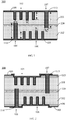
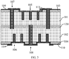
- FIG. 1 shows a schematic diagram of a double-sided capacitor 100 according to an embodiment of the present application, that is, a schematic diagram of a longitudinal section of the double-sided capacitor 100.
- the double-sided capacitor 100 includes a first semiconductor layer 101, an intermediate insulating layer 120, a first insulating layer 109, a second insulating layer 110, a second semiconductor layer 102, a first electrode layer 113, and a second electrode layer 114, where the intermediate insulating layer 120 is disposed between the first semiconductor layer 101 and the second semiconductor layer 102.
- the first semiconductor layer 101 is provided with at least one first trench 105 and at least one second trench 107, and in this example, four first trenches 105 and one second trench 107 are taken as example as shown in FIG. 1 .
- the first trench 105 and the second trench 107 extend downward from an upper surface of the first semiconductor layer 101, a depth of the first trench 105 is less than a thickness of the first semiconductor layer 101, that is, the first trench 105 does not penetrate through the first semiconductor layer 101, and the second trench 107 penetrates through the first semiconductor layer 101 and the intermediate insulating layer 120.
- the second semiconductor layer 102 is provided with at least one third trench 106 and at least one fourth trench 108, the third trench 106 and the fourth trench 108 extend upward from a lower surface of the second semiconductor layer 102, a depth of the third trench 106 is less than a thickness of the second semiconductor layer 102, that is, the third trench 106 does not penetrate through the second semiconductor layer 102, the fourth trench 108 penetrates through the second semiconductor layer 102 and the intermediate insulating layer 120, and any two of the at least one first trench 105, the at least one second trench 107, the at least one third trench 106, and the at least one fourth trench 108 are not communicated.
- the first electrode layer 113 is disposed above the first semiconductor layer 101, in the at least one first trench 105, and in the at least one second trench 107; and the first insulating layer 109 is disposed between the first electrode layer 113 and the first semiconductor layer 101, the first electrode layer 113 is electrically isolated from the first semiconductor layer 101 through the first insulating layer 109, and electrically connected to the second semiconductor layer 102 through a bottom of the at least one second trench 107.
- the second electrode layer 114 is disposed below the second semiconductor layer 102, in the at least one third trench 106, and in the at least one fourth trench 108; and the second insulating layer 110 is disposed between the second electrode layer 114 and the second semiconductor layer 102, the second electrode layer 114 is electrically isolated from the second semiconductor layer 102 through the second insulating layer 110, and electrically connected to the first semiconductor layer 101 through a bottom of the at least one fourth trench 108.
- the first electrode layer 113 and the second electrode layer 114 are used as two electrodes of the double-sided capacitor, respectively.
- the trench may be a hole with a small difference in length and width of a cross section, or a trench with a large difference in length and width.
- a depth D 1 of the first trench 105 is less than a depth D 2 of the second trench 107, and a depth D 3 of the third trench 106 is less than a depth D 4 of the fourth trench 108.
- a width W 1 of the first trench 105 may be less than a width W 2 of the second trench 107 and a width W 3 of the third trench 106 may be less than a width W 4 of the fourth trench 108.
- the width may also be referred to as the opening size, or is also equivalent to a maximum spacing of an inner wall of the trench, that is, an opening size of the first trench 105 is less than an opening size of the second trench 107, and an opening size of the third trench 106 can be less than an opening size of the fourth trench 108; in other words, a maximum spacing of an inner wall of the first trench 105 is less than a maximum spacing of an inner wall of the second trench 107, and a maximum spacing of an inner wall of the third trench 106 may be less than a maximum spacing of an inner wall of the fourth trench 108.
- a width of a shape of the first trench 105 is less than a width of the second trench 107; on any cross section of the second semiconductor layer 102, a width of the third trench 106 is less than a width of the fourth trench 108, the width here is the opening size of the trench, and the width may refer to a width value at a maximum width of the trench.
- the first semiconductor layer 101 may include the plurality of first trenches 105 whose shapes of cross sections may be the same or different; similarly, the first semiconductor layer 101 may include the plurality of second trenches 107 whose shapes of cross sections may be the same or different; correspondingly, shapes of cross sections of the plurality of third trenches 106 included in the second semiconductor layer 102 may be the same or different, and shapes of cross sections of the plurality of fourth trenches 108 may be the same or different.
- a shape of a cross section of the first trench 105 and a shape of a cross section of the second trench 107 may the same or different.
- a cross section of the first trench 105 is circular, that is, the first trench 105 is a circular hole
- a cross section of the second trench 107 is rectangular, that is, the second trench 107 is a square hole, as shown in FIG. 7 ; alternatively, a cross section of the first trench 105 and a cross section of the second trench 107 are both circular, and both of them are circular holes.
- a shape of a cross section of the third trench 106 and a shape of a cross section of the fourth trench 108 may be the same or different.
- shapes of cross sections of the first trench 105, the second trench 107, the third trench 106, and the fourth trench 108 may be different from each other or may be the same.
- a double-sided capacitor 100 may further include a first passivation insulating layer 103 disposed between a first semiconductor layer 101 and a first insulating layer 109; at least one first trench 105 and at least one second trench 107 extend through the first passivation insulating layer 103, and the first passivation insulating layer 103 may be configured to electrically isolate the first electrode layer 113 from the first semiconductor layer 101.
- the double-sided capacitor 100 may further include a second passivation insulating layer 104 disposed between a second semiconductor layer 102 and a second insulating layer 110; at least one third trench 106 and at least one fourth trench 108 penetrate through the second passivation insulating layer 104, and the second passivation insulating layer 104 may be configured to electrically isolate the second electrode layer 114 from the second semiconductor layer 102.
- the first passivation insulating layer 103 may be disposed on the first semiconductor layer 101 having a larger area, such as left and right regions of the first semiconductor layer 101 shown in FIG.
- the second passivation insulating layer 104 may be disposed on the second semiconductor layer 102 having a larger area, such as left and right regions of the lower layer shown in FIG. 2 , however the embodiment of the present application is not limited thereto.
- the upper layer and the lower layer of the double-sided capacitor 100 shown in FIGS. 1 and 2 are symmetrical, and the number of trenches included therein is also the same, where a symmetrical manner may be a central symmetry.
- the upper layer and lower layer may also be asymmetric, and the number of trenches included therein may also be different, which is not limited in the embodiment of the present application.
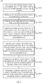
- FIG. 4 shows a schematic flowchart of a method 200 for fabricating a double-sided capacitor according to an embodiment of the present application.
- the method 200 includes: S210, providing an SOI substrate including a first semiconductor layer, an intermediate insulating layer and a second semiconductor layer from top to bottom; S220, etching the first semiconductor layer of the SOI substrate to form a first trench and a second trench; and S230, etching the second semiconductor layer to form a third trench and a fourth trench.
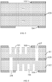
- an SOI substrate includes a first semiconductor layer 101, an intermediate insulating layer 120, and a second semiconductor layer 102, materials of the first semiconductor layer 101 and the second semiconductor layer 102 may be the same, for example, monocrystalline silicon, such as P-type monocrystalline silicon with resistivity about 1 m ⁇ cm; and the intermediate insulating layer 120 is made of an insulating material, for example, silicon dioxide.
- a thickness of each layer of the SOI substrate shown in FIG. 5 is only schematic and is independent of the actual thickness, for example, a thickness of the first semiconductor layer 101 may be 200 microns and a thickness of the intermediate insulating layer 120 may be 100 nanometers; alternatively, a thickness of the first semiconductor layer 101 is less than a thickness of the intermediate insulating layer 120; alternatively, a thickness of the first semiconductor layer 101 may be equal to a thickness of the second semiconductor layer 102, or may not be equal to a thickness of the second semiconductor layer 102, which is not limited in the embodiment of the present application.
- the method 200 may also include: growing a first passivation insulating layer on an upper surface of the first semiconductor layer; and similarly, before the etching the second semiconductor layer in S230, the method 200 may also include: growing a second passivation insulating layer on a lower surface of the second semiconductor layer. As shown in FIG. 6 , the first passivation insulating layer 103 is grown on the upper surface of the first semiconductor layer 101, and the second passivation layer 104 is grown on the lower surface of the second semiconductor 102.
- insulating passivation layers such as the first passivation insulating layer 103 and the passivation insulating layer 104 are fabricated on the upper and lower surfaces of the SOI substrate; and the passivation insulating layer may be grown by at least one of the following manners, here, description is made by an example of growing the first passivation insulating layer 103, it is also applicable to the second passivation insulating layer 104, and the growing manner may be the same or different.
- silicon dioxide is grown on the upper surface of the first semiconductor layer 101 as the passivation insulating layer 103 by means of thermal oxidation.
- PVD physical vapor deposition
- CVD chemical vapor deposition
- a silicon nitride or a silicon oxide such as unpoded silicon glass (USG) or silicon dioxide converted by tetraethyl orthosilicate (TEOS) or the like is grown as the passivation insulating layer 103.
- the passivation insulating layer 103 various sprayed or spin-coated polymers such as polyimide, parylene, benzocyclobutene (BCB) and the like are used as the passivation insulating layer 103; alternatively, the passivation insulating layer may also be a spin on glass (SOG), that is, amorphous phase silicon oxide obtained by spin-coating or spraying a silicide-containing solution on a silicon wafer, then performing heating to remove a solvent, and conducting curing.
- SOG spin on glass
- silicon dioxide is grown as the passivation insulating layers 103 and/or 104 by means of thermal oxidation.
- the first semiconductor layer 101 is etched to form at least one first trench 105 and at least one second trench 107, the first trench 105 and the second trench 107 are downward from an upper surface of the first semiconductor layer, a depth of the first trench 105 is less than a thickness of the first semiconductor layer 101, that is, the first trench 105 does not exceed the intermediate insulating layer 120, the second trench 107 penetrates through the first semiconductor layer 101 and the intermediate insulating layer 120, but the second trench does not penetrate through the second semiconductor layer 102.
- the second semiconductor layer 102 is etched to form at least one third trench 106 and at least one fourth trench 108, the third trench 106 and the fourth trench 108 are upward from a lower surface of the second semiconductor layer 102, a depth of the third trench 106 is less than a thickness of the second semiconductor layer 102, that is, the third trench 106 does not exceed the intermediate insulating layer 120, the fourth trench 108 penetrates through the second semiconductor layer 102 and the intermediate insulating layer 120, but the fourth trench 108 does not exceed the first semiconductor layer 101, and any two of the at least one first trench, the at least one second trench, the at least one third trench, and the at least one fourth trench are not communicated.
- the first trench 105 and the second trench 107 also penetrate through the first passivation insulating layer 103; and if the lower surface of the second semiconductor layer 102 is provided with the second passivation insulating layer 104, the third trench 106 and the fourth trench 108 also penetrate through the second passivation insulating layer 104.
- the order of etching the first semiconductor layer 101 and etching the second semiconductor layer 102 is not limited.
- the number of the first trenches 105 and the second trenches 107 in the embodiment of the present application may be one or more, and may be set according to actual application, for example, an appropriate number of the first trenches 105 and the second trenches 107 may be set according to an area of a cross section of the first semiconductor layer 101, and the embodiment of the present application is not limited thereto.
- patterns presented by any cross section of the first trench 105 and the second trench 107 in the first semiconductor layer 101 may be arbitrary; when there are a plurality of first trenches 105 or a plurality of second trenches 107, patterns of the plurality of first trenches 105 or the plurality of second trenches 107 may be the same or different, and a pattern of any one of the first trenches 105 and a pattern of any one of the second trenches 107 may be the same or different, for example, as shown in FIG. 7 , the plurality of first trenches 105 are all circular, one second trench 107 is rectangular, or may be any other regular or irregular patterns, and the embodiment of the present application is not limited thereto.
- first trenches 105 when there are a plurality of first trenches 105, they may be arranged in various ways, and positions of the first trenches 105 relative to the second trenches 107 may also be varied.
- the first trenches 105 are all circular holes arranged in a honeycomb, and are all located on one side of the second trench 107; for another example, the plurality of first trenches 105 may be arranged in other regular or irregular manners, and located on both sides of the second trench 107, and the embodiment of the present application is not limited thereto.
- the upper surface of the first semiconductor layer 101 or the upper surface of the first passivation insulating layer 103 is etched, for example, deep reactive ion etching (DRIE) that may include a ultra-low temperature type and a Bosch type may be used.
- DRIE deep reactive ion etching
- windows that are not covered with photoresist and have different opening sizes are partially formed on the surface of the first passivation insulating layer 103 by a photolithography process, that is, a first photoresist layer is spin-coated on the upper surface of the first passivation insulating layer 104, at least two first windows are partially opened on the first photoresist layer, the first passivation insulating layer and the first semiconductor layer are etched along the at least two first windows by means of deep reactive ion etching (DRIE), to form the at least one first trench 105 and the at least one second trench 107 in a direction perpendicular to the surface of the SOI substrate, and the photoresist layer is removed after the trenches are etched.
- DRIE deep reactive ion etching
- a trench having a smaller opening has a smaller etching depth
- a trench having a larger opening has a larger etching depth; and therefore as for at least one first trench 105 whose depth does not reach the intermediate insulating layer 120 of the SOI substrate, its opening is smaller, thus its depth is smaller, on the contrary, at least one second trench 107 that penetrates through the intermediate insulating layer 120 of the SOI substrate, but does not penetrate through the entire SOI substrate, its opening is larger, and thus its depth is larger.
- both sides of the SOI substrate have one or more trench structures that penetrate through the intermediate insulating layer 120 of the SOI substrate, that is, at least one second trench 107 and at least one fourth trench 108, which cannot be connected to each other to form a through hole penetrating through the entire SOI substrate.
- the embodiment of the present application does not limit a relative position of the first trench 105 and the second trench 107.
- the second trench 107 may be disposed to the right of all of the plurality of first trenches 105, or disposed at an intermediate position or other positions, or when there are a plurality of second trenches 107, positions of the plurality of second trenches 107 are not limited.
- positions of trenches of the double-sided capacitor 100 may be asymmetrical and the number of trenches may be different, and the embodiment of the present application is not limited thereto.
- the method 200 may further include: partially etching the first passivation insulating layer 103 and the second passivation insulating layer 104. Specifically, if the at least one first trench 105 has a large number and is arranged densely, for example, arranged in a honeycomb shown in FIG.
- the first passivation insulating layer 103 and the second passivation insulating layer 104 may be partially etched first, and a photoresist layer may be sequentially spin-coated on surfaces of the upper first passivation insulating layers 103 and the lower second passivation insulating layer 104, and after exposure and development, windows uncovered with photoresist are partially opened; parts of the first passivation insulating layer 103 and the second passivation insulating layer 104 that are not covered with photoresist are removed by etching; and finally, the photoresist is removed to obtain the structure shown in FIG. 5 , and furthermore the etching described in S220 and S230 is performed on the structure shown in FIG. 5 .
- An opening region formed by the first passivation insulating layer in FIG. 5 corresponds to a first trench region.
- an insulating material is deposited above the first semiconductor layer, on an inner surface of the at least one first trench and on an inner surface of the at least one second trench, and the insulating material at a bottom of the at least one second trench is removed to expose the second semiconductor layer, so that a remaining portion of the insulating material forms a first insulating layer 109.
- an insulating material is deposited below the second semiconductor layer, on an inner surface of the at least one third trench, and on an inner surface of the at least one fourth trench; and the insulating material at a bottom of the at least one fourth trench is removed to expose the first semiconductor layer, so that a remaining portion of the insulating material forms a second insulating layer 110.
- FIG. 8 shows a schematic structural diagram after an insulating material is formed on both sides of a semiconductor, and at this time, the insulating material at a bottom of a second trench 107 and a fourth trench 108 has not been removed.
- an insulating material is deposited on the upper surface of the first passivation insulating layer 103 to form a first insulating layer 109; and similarly, if an upper surface of a second semiconductor layer 102 includes a second passivation insulating layer 104, an insulating material is deposited on an upper surface of the second passivation insulating layer 104 to form a second insulating layer 110.
- first semiconductor layer 101 and the second semiconductor layer 102 may be sequentially processed or may be processed at the same time, which will not be repeatedly described here.
- an insulating material is deposited in a first trench 105, a second trench 107 and above a first semiconductor layer 101, or when a first passivation insulating layer 103 is disposed above the first semiconductor layer 101, an insulating material is deposited on an upper surface of the first passivation insulating layer 103, and the deposited insulating material is a first insulating layer 109.
- a silicon dioxide layer is grown as the first insulating layer 109 by means of thermal oxidation, or by means of atomic layer deposition (ALD), PVD, CVD, spin-coating, or the like.
- a material of the first insulating layer 109 may include a silicon oxide, a silicon nitride, a metal oxide, a metal nitride, or the like, such as silicon dioxide, silicon nitride, aluminum oxide, aluminum nitride, hafnium oxide, zirconium oxide, zinc oxide, titanium dioxide, lead zirconate titanate, or the like.
- the first insulating layer 109 may be one layer, two or more layers, and a material of each layer may be the same or different. A specific material and a thickness of the layer may be adjusted according to a capacitance, frequency characteristic, loss and other requirements of the capacitor, and the embodiment of the present application is not limited thereto.
- ALD is a mature developed technology in recent years to deposit substances on a surface of an object layer by layer in the form of a monoatomic layer.
- ALD has advantages of excellent step coverage, film thickness uniformity, film continuity and material quality.
- ALD may already realize the deposition of a high-k insulating dielectric material such as alumina, hafnium oxide and zirconia.
- the material of the first passivation insulating layer 103 may be the same as or different from that of the first insulating layer 109.
- the insulating material at the bottom of the second trench 107 needs to be removed so that the insulating material is broken at the bottom of the second trench 107, and the second semiconductor layer 102 is exposed through the bottom.
- the insulating material at the bottom of the fourth trench 108 is removed so that the insulating material is broken at the bottom of the fourth trench 108, and the first semiconductor layer 101 is exposed through the bottom.
- each second trench 107 needs to be removed correspondingly; and similarly, if plurality of fourth trenches 108 are included, the insulating material at the bottom of each fourth trench 108 needs to be removed correspondingly.
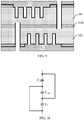
- the insulating material at the bottom may be removed in various manners. For example, as shown in FIG. 9 , first a layer of a dry film is attached to a surface of an SOI substrate, such as a dry film 111 attached to an upper surface of a first passivation insulating layer 103 and a dry film 112 attached to an upper surface of a second passivation insulating layer 104 in FIG. 9 , then a window is opened at each of a plurality of second trenches 107 with larger openings by photolithography, and finally the insulating material at a bottom of each of the second trenches 107 is removed by plasma etching, and similarly, the insulating material at a bottom of each of fourth trenches 108 is removed.
- the dry films 111 and 112 are removed after the insulating material at the bottom is removed.
- a conductive material is deposited above the first semiconductor layer, in the at least one first trench and in the at least one second trench where the insulating material is deposited, to form a first electrode layer; as shown in FIGS. 1 to 3 , the first electrode layer 113 is electrically isolated from the first semiconductor layer 101 through the first insulating layer 109 and is electrically connected to the second semiconductor layer 102 through the bottom of the at least one second trench 107.
- a conductive material is deposited below the second semiconductor layer, in the at least one third trench and in the at least one fourth trench where the insulating material is deposited, to form a second electrode layer; as shown in FIGS. 1 to 3 , the second electrode layer 114 is electrically isolated from the second semiconductor layer 102 through the second insulating layer 110 and is electrically connected to the first semiconductor layer 101 through the bottom of the at least one fourth trench 108.
- the conductive material may be heavily doped polysilicon, or various metals such as aluminum, tungsten, copper, and the like, may also be a carbon-based material, or a low-resistivity compound such as titanium nitride, or a combination of the foregoing conductive materials, and the embodiment of the present application is not limited thereto.
- the processing order of the upper and lower capacitors of the SOI substrate is not limited, for example, the capacitors may be synchronously fabricated on both sides of the SOI substrate; alternatively, first a front side of the SOI wafer may be processed to fabricate an upper capacitor and a conductive channel, then a back side of the SOI wafer is processed to fabricate a lower capacitor and a back conductive channel, and the double-sided capacitor structure proposed by the present application may also be realized by the way of first processing the front side and then the back side.
- Step 1 an SOI substrate is selected, an upper layer of the SOI substrate is a first semiconductor layer 101, which is heavily doped monocrystalline silicon with a thickness of 200 microns (with resistivity of 1 m ⁇ cm), an intermediate layer thereof is an intermediate insulating layer 120, which is silicon dioxide with a thickness of 100 nanometers, and a lower layer thereof is a second semiconductor layer 102, which is heavily doped monocrystalline silicon with a thickness of 200 microns (with resistivity of 1 m ⁇ cm).
- the SOI wafer is placed in a high temperature furnace tube, in which a mixed gas of hydrogen and oxygen is introduced, and oxidized at a high temperature of 1150 °C for 2 hours.
- Silicon dioxide with a thickness about 1 micron is grown on the surface of the wafer, namely the first passivation insulating layer 103 and the second passivation insulating layer 104; then a photoresist layer is sequentially spin-coated on surfaces of the upper and lower layers of silicon dioxide, and after exposure and development, a window not covered with photoresist is partially opened; then the wafer is etched in a BOE solution with a ratio of 1:5 HF (49%): NH4F (40%) for 15 minutes to remove silicon dioxide uncovered with photoresist. Finally, the photoresist is removed to obtain the structure shown in FIG. 5 .
- Step 2 a layer of photoresist is spin-coated on an upper surface of the SOI wafer, and after exposure and development, windows of a circular hole array with diameters of 5 microns and a rectangular window with a length of 30 microns and a width of 10 microns are respectively opened, and the arrangement of the two windows is shown in FIG. 7 .
- a deep hole array and a trench are etched on the upper silicon by a DRIE process, and the deep hole array is an array formed by the first trenches 105 and the trench is the second trench 107, as shown in FIG. 6 .
- a depth of the first trench 105 is 70 microns and a depth of the second trench 107 is 205 microns.
- a deep hole array with a depth of 70 microns and a trench with a depth of 205 microns, which are a third trench and a fourth trench respectively are etched on the lower silicon of the SOI wafer. Finally, the photoresist is removed to obtain the structure shown in FIG. 6 .
- Step 3 using an ALD technology, 33 nm of hafnium oxide is deposited on surfaces of the first passivation insulating layer 103, the first trench 105 and the second trench 107 on the upper layer of the wafer as the first insulating layer 109, and 33 nm of hafnium oxide is deposited on surfaces of the second passivation insulating layer 104, the third trench 106 and the fourth trench 108 on the lower layer of the wafer as the second insulating layer 110, as shown in FIG. 8 .
- Step 4 dry films 111 and 112 are covered on the upper and lower surfaces of the SOI wafer. After exposure and development, windows are opened at the second trench 107 and the fourth trench 108. The hafnium oxide at the bottom of trenches 107 and 108 is removed by means of plasma etching, as shown in FIG. 9 . Finally, the dry films 111 and 112 are removed.
- Step 5 after Step 4, a layer of titanium and a layer of copper are first deposited in the first trench 105, the third trench 106, the second trench 107 and the fourth trench 108 by means of PVD, as a barrier layer and a seed layer for electroplating. Then, all deep holes and trenches are filled with copper by means of double-sided electroplating. Finally, a conductive material at the corners is removed by means of photolithography to form upper and lower electrodes of the capacitor, that is, the first electrode layer 113 and the second electrode layer 114, as shown in FIG. 2 .
- a trench structure having a depth not reaching an intermediate insulating layer and a trench structure having a depth exceeding the intermediate insulating layer are etched on both sides of an SOI substrate; an insulating dielectric film and a conductive material are sequentially deposited on a surface of the trench having the depth not reaching the intermediate insulating layer to form a capacitor; after an insulating dielectric film is deposited on a surface of the trench having the depth exceeding the intermediate insulating layer and the dielectric material at the bottom is removed, a conductive material is filled in the trench structure having the depth exceeding the intermediate insulating layer to become a conductive channel.
- At least one channel is insulated from an upper layer of the SOI substrate and is electrically connected to a lower layer of the SOI substrate; and at least one channel is insulated from the lower layer of the SOI substrate and is electrically connected to the upper layer of the SOI substrate.
- front and back sides of the SOI wafer are respectively provided with a 3D capacitor fabricated based on a semiconductor process: an upper capacitor C 1 and a lower capacitor C 2 ; the SOI wafer itself has a substrate capacitor (C sub ); and the three capacitors are connected in parallel as shown in FIG. 10 through a conductive channel penetrating through the intermediate insulating layer of the SOI substrate, which is referred to as a large capacitor. Not only could etching a trench penetrating through the substrate be avoided so that an entire structure has stronger mechanical strength, but also a capacitance is larger utilizing a substrate capacitance of an SOI wafer itself.
- B corresponding to A indicates that B is associated with A, and B may be determined based on A.
- determining B based on A does not mean that B is determined based on A only; and B may also be determined based on A and/or other information.
- sequence numbers of the foregoing processes do not mean execution sequences in various embodiments of the present application.
- the execution sequences of the processes should be determined according to functions and internal logic of the processes, and should not be construed as any limitation on the implementation processes of the embodiments of the present application.
Landscapes
- Semiconductor Integrated Circuits (AREA)
Claims (14)
- Doppelseitiger Kondensator, umfassend:eine isolierende Zwischenschicht (120), die zwischen einer ersten Halbleiterschicht (101) und einer zweiten Halbleiterschicht (102) angeordnet ist;wobei die erste Halbleiterschicht (101) mit einem ersten Graben (105) und einem zweiten Graben (107) versehen ist, wobei der erste Graben (105) und der zweite Graben (107) von einer oberen Oberfläche der ersten Halbleiterschicht (101) nach unten verlaufen, eine Tiefe des ersten Grabens (105) geringer ist als eine Dicke der ersten Halbleiterschicht (101) und der zweite Graben (107) durch die erste Halbleiterschicht (101) und die isolierende Zwischenschicht (120) hindurchgeht und nach unten zur zweiten Halbleiterschicht (102) reicht;wobei die zweite Halbleiterschicht (102) mit einem dritten Graben (106) und einem vierten Graben (108) versehen ist, wobei der dritte Graben (106) und der vierte Graben (108) von einer unteren Oberfläche der zweiten Halbleiterschicht (102) nach oben verlaufen, eine Tiefe des dritten Grabens (106) geringer ist als eine Dicke der zweiten Halbleiterschicht (102), der vierte Graben (108) durch die zweite Halbleiterschicht (102) und die isolierende Zwischenschicht (120) hindurchgeht und nach unten zur ersten Halbleiterschicht (101) reicht;wobei zwei beliebige des ersten Grabens (105), des zweiten Grabens (107), des dritten Grabens (106) und des vierten Grabens (108) nicht miteinander verbunden sind;eine erste Elektrodenschicht (113), die über der ersten Halbleiterschicht (101), in dem ersten Graben (105) und in dem zweiten Graben (107) angeordnet ist;eine erste isolierende Schicht (109), die zwischen der ersten Elektrodenschicht (113) und der ersten Halbleiterschicht (101) angeordnet ist, um die erste Elektrodenschicht (113) in dem ersten Graben (105) und in dem zweiten Graben (107) von der ersten Halbleiterschicht (101) zu isolieren, und an einem Boden des zweiten Grabens (107) unterbrochen ist, um die erste Elektrodenschicht (113) mit der zweiten Halbleiterschicht elektrisch zu verbinden;eine zweite Elektrodenschicht (114), die unter der zweiten Halbleiterschicht (102), in dem dritten Graben (106) und in dem vierten Graben (108) angeordnet ist; undeine zweite isolierende Schicht (110), die zwischen der zweiten Elektrodenschicht (114) und der zweiten Halbleiterschicht (102) angeordnet ist, um die zweite Elektrodenschicht (114) in dem dritten Graben (106) und in dem vierten Graben (108) von der zweiten Halbleiterschicht (102) zu isolieren, und an einem Boden des vierten Grabens (107) unterbrochen ist, um die zweite Elektrodenschicht (114) mit der ersten Halbleiterschicht (101) elektrisch zu verbinden;wobei die erste Halbleiterschicht (101), die isolierende Zwischenschicht (120) und die zweite Halbleiterschicht (102) von oben nach unten in vertikaler Richtung senkrecht zu ihren Hauptoberflächen gestapelt sind, um ein SOI-Substrat zu bilden, Materialien der ersten Halbleiterschicht (101) und der zweiten Halbleiterschicht (102) monokristallines Silicium mit einem Widerstand von 1 mΩ-cm sind, Materialien der mittleren isolierenden Schicht (120) Siliciumdioxid sind.
- Kondensator nach Anspruch 1, wobei eine Breite eines beliebigen Querschnitts des ersten Grabens (105) parallel zu einer Oberfläche der ersten Halbleiterschicht (101) kleiner ist als eine Breite eines beliebigen Querschnitts des zweiten Grabens (107) parallel zu einer Oberfläche der ersten Halbleiterschicht (101); und/oder
eine Breite eines beliebigen Querschnitts des dritten Grabens (106) parallel zu einer Oberfläche der zweiten Halbleiterschicht (102) kleiner ist als eine Breite eines beliebigen Querschnitts des vierten Grabens (108) parallel zu einer Oberfläche der zweiten Halbleiterschicht (102) - Kondensator nach Anspruch 1 oder 2, wobei der Kondensator ferner umfasst:eine erste isolierende Passivierungsschicht (103), die zwischen der ersten Halbleiterschicht (101) und der ersten isolierenden Schicht (109) angeordnet ist, wobei der erste Graben (105) und der zweite Graben (107) durch die erste isolierende Passivierungsschicht (103) hindurchgehen; und/odereine zweite isolierende Passivierungsschicht (104), die zwischen der zweiten Halbleiterschicht (102) und der zweiten isolierenden Schicht (110) angeordnet ist, wobei der dritte Graben (106) und der vierte Graben (108) durch die zweite isolierende Passivierungsschicht (104) hindurchgehen.
- Kondensator nach Anspruch 3, wobei Materialien der ersten isolierenden Passivierungsschicht (103) und/oder der zweiten isolierenden Passivierungsschicht (104) mindestens eines eines Siliciumoxids, eines Siliciumnitrids und eines Polymers sind.
- Kondensator nach einem der Ansprüche 1 bis 4, wobei eine Form eines Querschnitts des ersten Grabens (105) parallel zu einer Oberfläche der ersten Halbleiterschicht (101) von einer Form eines Querschnitts des zweiten Grabens (107) parallel zu einer Oberfläche der ersten Halbleiterschicht (101) verschieden ist, und/oder
eine Form eines Querschnitts des dritten Grabens (106) parallel zu einer Oberfläche der zweiten Halbleiterschicht (102) von einer Form eines Querschnitts des vierten Grabens (108) parallel zu einer Oberfläche der zweiten Halbleiterschicht (102) verschieden ist. - Kondensator nach einem der Ansprüche 1 bis 5, wobei die erste isolierende Schicht (109) und/oder die zweite isolierende Schicht (110) mindestens eine einer Siliciumoxidschicht, einer Siliciumnitridschicht, einer Metalloxidschicht und einer Metallnitridschicht umfassen.
- Kondensator nach einem der Ansprüche 1 bis 6, wobei die erste Elektrodenschicht (113) und/oder die zweite Elektrodenschicht (114) mindestens eine Schicht aus stark dotiertem Polysilicium, einem Material auf Kohlenstoffbasis, Metall und Titannitrid umfassen.
- Verfahren zum Herstellen eines doppelseitigen Kondensators, umfassend:Bereitstellen eines SOI-Substrats (S210), wobei das SOI-Substrat eine erste Halbleiterschicht (101), eine isolierende Zwischenschicht (120) und eine zweite Halbleiterschicht (102) von oben nach unten umfasst, die erste Halbleiterschicht, die isolierende Zwischenschicht und die zweite Halbleiterschicht in vertikaler Richtung senkrecht zu ihren Hauptoberflächen gestapelt sind, Materialien der ersten Halbleiterschicht und der zweiten Halbleiterschicht monokristallines Silicium mit einem Widerstand von 1 mΩ-cm sind, Materialien der mittleren isolierenden Schicht Siliciumdioxid sind;Ätzen der ersten Halbleiterschicht, um einen ersten Graben (105) und einen zweiten Graben (107) zu bilden (S220), wobei der erste Graben und der zweite Graben von einer oberen Oberfläche der ersten Halbleiterschicht nach unten verlaufen, eine Tiefe des ersten Grabens geringer ist als eine Dicke der ersten Halbleiterschicht und der zweite Graben durch die erste Halbleiterschicht und die isolierende Zwischenschicht hindurchgeht und nach unten zur zweiten Halbleiterschicht reicht;Ätzen der zweiten Halbleiterschicht, um einen dritten Graben (106) und einen vierten Graben (108) zu bilden (S220), wobei der dritte Graben und der vierte Graben von einer unteren Oberfläche der zweiten Halbleiterschicht nach oben verlaufen, eine Tiefe des dritten Grabens geringer ist als eine Dicke der zweiten Halbleiterschicht, der vierte Graben durch die zweite Halbleiterschicht hindurchgeht und nach unten zur ersten Halbleiterschicht reicht, und zwei beliebige des ersten Grabens, des zweiten Grabens, des dritten Grabens und des vierten Grabens nicht miteinander verbunden sind;Ablagern eines isolierenden Materials über der ersten Halbleiterschicht, auf einer inneren Oberfläche des ersten Grabens und auf einer inneren Oberfläche des zweiten Grabens und Entfernen des isolierenden Materials an einem Boden des zweiten Grabens derart, dass das isolierende Material an einem Boden des zweiten Grabens unterbrochen ist, um die zweite Halbleiterschicht zu exponieren (S240);Ablagern eines isolierenden Materials unter der zweiten Halbleiterschicht, auf einer inneren Oberfläche des dritten Grabens und auf einer inneren Oberfläche des vierten Grabens und Entfernen des isolierenden Materials an einem Boden des vierten Grabens derart, dass das isolierende Material an einem Boden des vierten Grabens unterbrochen ist, um die erste Halbleiterschicht zu exponieren (S250);Ablagern eines leitenden Materials über der ersten Halbleiterschicht, in dem ersten Graben und in dem zweiten Graben, wobei das isolierende Material abgelagert wird, um eine erste Elektrodenschicht (113) zu bilden (S260); undAblagern eines leitenden Materials unter der zweiten Halbleiterschicht, in dem dritten Graben und in dem vierten Graben, wobei das isolierende Material abgelagert wird, um eine zweite Elektrodenschicht (114) zu bilden (S270).
- Verfahren nach Anspruch 8, wobei das Ätzen der ersten Halbleiterschicht des SOI-Substrats, um den ersten Graben und den zweiten Graben zu bilden (S220), umfasst:Aufwachsen einer ersten isolierenden Passivierungsschicht auf der oberen Oberfläche der ersten Halbleiterschicht,Ätzen der ersten isolierenden Passivierungsschicht und der ersten Halbleiterschicht, um den ersten Graben und den zweiten Graben zu bilden, wobei der erste Graben und der zweite Graben durch die erste isolierende Passivierungsschicht hindurchgehen; und/oderdas Ätzen der zweiten Halbleiterschicht, um den dritten Graben und den vierten Graben zu bilden (S230), umfasst:Aufwachsen einer zweiten isolierenden Passivierungsschicht auf der unteren Oberfläche der zweiten Halbleiterschicht undÄtzen der zweiten isolierende Passivierungsschicht und der zweiten Halbleiterschicht, um den dritten Graben und den vierten Graben zu bilden, wobei der dritte Graben und der vierte Graben durch die zweite isolierende Passivierungsschicht hindurchgehen.
- Verfahren nach Anspruch 9, wobei das Ätzen der ersten isolierenden Passivierungsschicht und der ersten Halbleiterschicht umfasst:Schleuderbeschichten einer ersten Fotolackschicht auf einer oberen Oberfläche der ersten isolierenden Passivierungsschicht,teilweises Öffnen von mindestens zwei ersten Fenstern auf der ersten Fotolackschicht,Ätzen der ersten isolierenden Passivierungsschicht und der ersten Halbleiterschicht entlang den mindestens zwei ersten Fenstern, um den ersten Graben und den zweiten Graben zu bilden,Entfernen der ersten Fotolackschicht nach dem Ätzen; und/oderdas Aufwachsen der zweiten isolierenden Passivierungsschicht auf der unteren Oberfläche der zweiten Halbleiterschicht umfasst:Schleuderbeschichten einer zweiten Fotolackschicht auf einer oberen Oberfläche der zweiten isolierenden Passivierungsschicht,teilweises Öffnen von mindestens zwei zweiten Fenstern auf der zweiten Fotolackschicht,Ätzen der zweiten isolierende Passivierungsschicht und der zweiten Halbleiterschicht entlang den mindestens zwei zweiten Fenstern, um den dritten Graben und den vierten Graben zu bilden, undEntfernen der zweiten Fotolackschicht nach dem Ätzen.
- Verfahren nach Anspruch 9 oder 10, wobei das Aufwachsen der ersten isolierenden Passivierungsschicht und/oder der zweiten isolierenden Passivierungsschicht umfasst:Aufwachsen einer Siliciumdioxidschicht durch thermische Oxidation, wobei die erste isolierende Passivierungsschicht und/oder die zweite isolierende Passivierungsschicht die Siliciumdioxidschicht umfassen; und/oderAufwachsen einer Siliciumnitridschicht oder einer Siliciumoxidschicht durch physikalische Aufdampfung und/oder chemische Aufdampfung, wobei die erste isolierende Passivierungsschicht und/oder die zweite isolierende Passivierungsschicht die Siliciumnitridschicht und/oder die Siliciumoxidschicht umfasst; und/oderSprühen und/oder Schleuderbeschichten einer Polymerschicht oder einer auf Glas geschleuderten Schicht, wobei die erste isolierende Passivierungsschicht und/oder die zweite isolierende Passivierungsschicht die Polymerschicht oder die auf Glas geschleuderte Schicht umfassen.
- Verfahren nach einem der Ansprüche 8 bis 11, wobei das Ätzen tiefes reaktives Ionenätzen ist.
- Verfahren nach einem der Ansprüche 8 bis 12, wobei das Ablagern des isolierenden Materials umfasst:Aufwachsen von Siliciumdioxid durch thermische Oxidation, wobei das isolierende Material das Siliciumdioxid umfasst; und/oderAblagern des isolierenden Materials durch mindestens eines von physikalischer Aufdampfung, chemischer Aufdampfung, Atomschichtabscheidung, Sprühen und Schleuderbeschichten.
- Verfahren nach einem der Ansprüche 8-13, wobei das Ablagern des leitenden Materials umfasst:
Ablagern des leitenden Materials durch mindestens eines von Atomschichtabscheidung, physikalischer Aufdampfung, metallorganischer chemischer Aufdampfung, Aufdampfung und Elektroplattieren.
Applications Claiming Priority (1)
| Application Number | Priority Date | Filing Date | Title |
|---|---|---|---|
| PCT/CN2018/099402 WO2020029119A1 (zh) | 2018-08-08 | 2018-08-08 | 双面电容器及其制作方法 |
Publications (3)
| Publication Number | Publication Date |
|---|---|
| EP3627558A1 EP3627558A1 (de) | 2020-03-25 |
| EP3627558A4 EP3627558A4 (de) | 2020-06-17 |
| EP3627558B1 true EP3627558B1 (de) | 2021-06-23 |
Family
ID=69413361
Family Applications (1)
| Application Number | Title | Priority Date | Filing Date |
|---|---|---|---|
| EP18914929.7A Active EP3627558B1 (de) | 2018-08-08 | 2018-08-08 | Doppelseitiger kondensator und herstellungsverfahren dafür |
Country Status (4)
| Country | Link |
|---|---|
| US (1) | US10991793B2 (de) |
| EP (1) | EP3627558B1 (de) |
| CN (1) | CN111615750B (de) |
| WO (1) | WO2020029119A1 (de) |
Families Citing this family (14)
| Publication number | Priority date | Publication date | Assignee | Title |
|---|---|---|---|---|
| CN113497037B (zh) * | 2020-03-20 | 2023-07-04 | 长鑫存储技术有限公司 | 双面电容结构及其形成方法 |
| CN111354788B (zh) * | 2020-03-24 | 2023-05-16 | 成都森未科技有限公司 | 一种深沟槽绝缘栅极器件及其制备方法 |
| CN113764580B (zh) * | 2020-06-04 | 2023-09-12 | 长鑫存储技术有限公司 | 双面电容结构及其形成方法 |
| CN112018096B (zh) * | 2020-07-31 | 2022-05-24 | 复旦大学 | 一种用于能量缓冲的纳米电容三维集成系统及其制备方法 |
| CN112151535B (zh) * | 2020-08-17 | 2022-04-26 | 复旦大学 | 一种硅基纳米电容三维集成结构及其制备方法 |
| CN112201655B (zh) * | 2020-09-10 | 2022-04-29 | 复旦大学 | 一种纳米电容三维集成结构及其制作方法 |
| CN114188480B (zh) * | 2020-09-14 | 2025-07-29 | 安徽寒武纪信息科技有限公司 | 一种电容器结构及其形成电容器结构的方法 |
| CN115513127B (zh) * | 2021-06-23 | 2025-05-16 | 格科半导体(上海)有限公司 | 沟槽填充方法及半导体器件 |
| US11869988B2 (en) * | 2021-08-26 | 2024-01-09 | Taiwan Semiconductor Manufacturing Company, Ltd. | Double-sided stacked DTC structure |
| US12040353B2 (en) * | 2021-08-27 | 2024-07-16 | Taiwan Semiconductor Manufacturing Company Limited | Multi-tier deep trench capacitor and methods of forming the same |
| US20230135677A1 (en) * | 2021-11-01 | 2023-05-04 | The Johns Hopkins University | Nanostructure materials and fabrication methods |
| KR20230088565A (ko) | 2021-12-10 | 2023-06-20 | 삼성전자주식회사 | 반도체 메모리 소자 |
| CN115295726A (zh) * | 2022-10-08 | 2022-11-04 | 成都宏科电子科技有限公司 | 一种3d硅基电容器及其制备方法 |
| TWI862432B (zh) * | 2024-03-11 | 2024-11-11 | 華邦電子股份有限公司 | 3d電容結構及其製造方法 |
Family Cites Families (17)
| Publication number | Priority date | Publication date | Assignee | Title |
|---|---|---|---|---|
| DE4321638A1 (de) * | 1992-09-19 | 1994-03-24 | Samsung Electronics Co Ltd | Halbleiterspeicherbauelement mit einem Kondensator und Verfahren zu seiner Herstellung |
| US5583359A (en) | 1995-03-03 | 1996-12-10 | Northern Telecom Limited | Capacitor structure for an integrated circuit |
| IT1314154B1 (it) * | 1999-12-21 | 2002-12-04 | St Microelectronics Srl | Struttura a condensatore verticale ad alta densita' di integrazione erelativo processo di fabbricazione |
| US6794245B2 (en) * | 2002-07-18 | 2004-09-21 | Micron Technology, Inc. | Methods of fabricating double-sided hemispherical silicon grain electrodes and capacitor modules |
| CN100365798C (zh) | 2003-06-20 | 2008-01-30 | 皇家飞利浦电子股份有限公司 | 电子器件、组件及制造电子器件的方法 |
| DE102007009383A1 (de) * | 2007-02-20 | 2008-08-21 | Fraunhofer-Gesellschaft zur Förderung der angewandten Forschung e.V. | Halbleiteranordnung und Verfahren zu deren Herstellung |
| US8227847B2 (en) | 2008-02-20 | 2012-07-24 | Nxp B.V. | Ultra high density capacity comprising pillar-shaped capacitors formed on both sides of a substrate |
| EP2519967B1 (de) * | 2009-12-30 | 2014-12-10 | Solexel, Inc. | Mobile elektrostatische träger zur verarbeitung eines dünnen wafers |
| CN102376780B (zh) * | 2010-08-16 | 2013-09-25 | 众智光电科技股份有限公司 | 具有嵌入式高密度电容的硅基座 |
| JP5724635B2 (ja) * | 2011-05-26 | 2015-05-27 | 株式会社デンソー | 半導体装置およびその製造方法 |
| US9184041B2 (en) * | 2013-06-25 | 2015-11-10 | Taiwan Semiconductor Manufacturing Co., Ltd. | Integrated circuit with backside structures to reduce substrate warp |
| FR3012237B1 (fr) * | 2013-10-22 | 2017-03-03 | Commissariat Energie Atomique | Puce electronique comprenant des moyens de protection de sa face arriere |
| DE102014200869B4 (de) * | 2013-11-22 | 2018-09-20 | Fraunhofer-Gesellschaft zur Förderung der angewandten Forschung e.V. | Integrierter Kondensator und Verfahren zum Herstellen desselben und dessen Verwendung |
| DE102014223904A1 (de) * | 2014-11-24 | 2016-05-25 | Fraunhofer-Gesellschaft zur Förderung der angewandten Forschung e.V. | Kondensator und Verfahren zum Herstellen desselben |
| WO2017145515A1 (ja) * | 2016-02-22 | 2017-08-31 | 株式会社村田製作所 | 半導体コンデンサおよび電源モジュール |
| US9929085B2 (en) * | 2016-06-02 | 2018-03-27 | Globalfoundries Inc. | Integrated circuit structure having deep trench capacitor and through-silicon via and method of forming same |
| US10229789B2 (en) * | 2016-10-28 | 2019-03-12 | Samsung Electro-Mechanics Co., Ltd. | Multilayer thin-film capacitor |
-
2018
- 2018-08-08 CN CN201880001021.1A patent/CN111615750B/zh active Active
- 2018-08-08 EP EP18914929.7A patent/EP3627558B1/de active Active
- 2018-08-08 WO PCT/CN2018/099402 patent/WO2020029119A1/zh not_active Ceased
-
2019
- 2019-10-22 US US16/659,574 patent/US10991793B2/en active Active
Also Published As
| Publication number | Publication date |
|---|---|
| US10991793B2 (en) | 2021-04-27 |
| US20200058732A1 (en) | 2020-02-20 |
| CN111615750A (zh) | 2020-09-01 |
| EP3627558A4 (de) | 2020-06-17 |
| EP3627558A1 (de) | 2020-03-25 |
| CN111615750B (zh) | 2023-06-23 |
| WO2020029119A1 (zh) | 2020-02-13 |
Similar Documents
| Publication | Publication Date | Title |
|---|---|---|
| EP3627558B1 (de) | Doppelseitiger kondensator und herstellungsverfahren dafür | |
| US11063113B2 (en) | Capacitor and method for fabricating the same | |
| CN112602191B (zh) | 电容器及其制作方法 | |
| CN111971791B (zh) | 电容器及其制作方法 | |
| CN110785840A (zh) | 电容器及其制作方法 | |
| US11276750B2 (en) | Capacitor and method for fabricating the same | |
| US11903182B2 (en) | Capacitor and manufacturing method therefor | |
| CN102683318A (zh) | 硅电容器内部多层电极连接结构及连接方法 | |
| CN102569250A (zh) | 高密度电容器及其电极引出方法 | |
| CN112119476B (zh) | 电容器及其制作方法 | |
| US11362171B2 (en) | Capacitor and manufacturing method therefor | |
| WO2020215260A1 (zh) | 电容器及其制备方法 | |
| US11239308B2 (en) | Capacitor and method for producing capacitor | |
| US11183602B2 (en) | Trench capacitor and method for manufacturing the same | |
| CN112189257A (zh) | 电容器及其制作方法 | |
| WO2021196016A1 (zh) | 电容器、电容结构、电容器的制作方法 | |
| CN110998856B (zh) | 电容器及其制作方法 | |
| CN121335187A (zh) | 硅电容及其制作方法、电子器件 |
Legal Events
| Date | Code | Title | Description |
|---|---|---|---|
| STAA | Information on the status of an ep patent application or granted ep patent |
Free format text: STATUS: UNKNOWN |
|
| STAA | Information on the status of an ep patent application or granted ep patent |
Free format text: STATUS: THE INTERNATIONAL PUBLICATION HAS BEEN MADE |
|
| PUAI | Public reference made under article 153(3) epc to a published international application that has entered the european phase |
Free format text: ORIGINAL CODE: 0009012 |
|
| STAA | Information on the status of an ep patent application or granted ep patent |
Free format text: STATUS: REQUEST FOR EXAMINATION WAS MADE |
|
| 17P | Request for examination filed |
Effective date: 20191022 |
|
| AK | Designated contracting states |
Kind code of ref document: A1 Designated state(s): AL AT BE BG CH CY CZ DE DK EE ES FI FR GB GR HR HU IE IS IT LI LT LU LV MC MK MT NL NO PL PT RO RS SE SI SK SM TR |
|
| AX | Request for extension of the european patent |
Extension state: BA ME |
|
| A4 | Supplementary search report drawn up and despatched |
Effective date: 20200520 |
|
| RIC1 | Information provided on ipc code assigned before grant |
Ipc: H01L 29/00 20060101AFI20200514BHEP Ipc: H01L 29/41 20060101ALI20200514BHEP Ipc: H01L 29/94 20060101ALI20200514BHEP |
|
| REG | Reference to a national code |
Ref country code: DE Ref legal event code: R079 Ref document number: 602018019149 Country of ref document: DE Free format text: PREVIOUS MAIN CLASS: H01L0029000000 Ipc: H01L0027060000 |
|
| RIC1 | Information provided on ipc code assigned before grant |
Ipc: H01L 29/00 20060101ALI20210208BHEP Ipc: H01L 27/12 20060101ALI20210208BHEP Ipc: H01L 27/08 20060101ALI20210208BHEP Ipc: H01L 29/94 20060101ALI20210208BHEP Ipc: H01L 27/06 20060101AFI20210208BHEP Ipc: H01L 29/41 20060101ALI20210208BHEP |
|
| GRAP | Despatch of communication of intention to grant a patent |
Free format text: ORIGINAL CODE: EPIDOSNIGR1 |
|
| STAA | Information on the status of an ep patent application or granted ep patent |
Free format text: STATUS: GRANT OF PATENT IS INTENDED |
|
| DAV | Request for validation of the european patent (deleted) | ||
| DAX | Request for extension of the european patent (deleted) | ||
| INTG | Intention to grant announced |
Effective date: 20210323 |
|
| GRAS | Grant fee paid |
Free format text: ORIGINAL CODE: EPIDOSNIGR3 |
|
| GRAA | (expected) grant |
Free format text: ORIGINAL CODE: 0009210 |
|
| STAA | Information on the status of an ep patent application or granted ep patent |
Free format text: STATUS: THE PATENT HAS BEEN GRANTED |
|
| AK | Designated contracting states |
Kind code of ref document: B1 Designated state(s): AL AT BE BG CH CY CZ DE DK EE ES FI FR GB GR HR HU IE IS IT LI LT LU LV MC MK MT NL NO PL PT RO RS SE SI SK SM TR |
|
| REG | Reference to a national code |
Ref country code: GB Ref legal event code: FG4D |
|
| REG | Reference to a national code |
Ref country code: CH Ref legal event code: EP |
|
| REG | Reference to a national code |
Ref country code: DE Ref legal event code: R096 Ref document number: 602018019149 Country of ref document: DE Ref country code: AT Ref legal event code: REF Ref document number: 1405051 Country of ref document: AT Kind code of ref document: T Effective date: 20210715 |
|
| REG | Reference to a national code |
Ref country code: IE Ref legal event code: FG4D |
|
| REG | Reference to a national code |
Ref country code: LT Ref legal event code: MG9D |
|
| PG25 | Lapsed in a contracting state [announced via postgrant information from national office to epo] |
Ref country code: HR Free format text: LAPSE BECAUSE OF FAILURE TO SUBMIT A TRANSLATION OF THE DESCRIPTION OR TO PAY THE FEE WITHIN THE PRESCRIBED TIME-LIMIT Effective date: 20210623 Ref country code: LT Free format text: LAPSE BECAUSE OF FAILURE TO SUBMIT A TRANSLATION OF THE DESCRIPTION OR TO PAY THE FEE WITHIN THE PRESCRIBED TIME-LIMIT Effective date: 20210623 Ref country code: FI Free format text: LAPSE BECAUSE OF FAILURE TO SUBMIT A TRANSLATION OF THE DESCRIPTION OR TO PAY THE FEE WITHIN THE PRESCRIBED TIME-LIMIT Effective date: 20210623 Ref country code: BG Free format text: LAPSE BECAUSE OF FAILURE TO SUBMIT A TRANSLATION OF THE DESCRIPTION OR TO PAY THE FEE WITHIN THE PRESCRIBED TIME-LIMIT Effective date: 20210923 |
|
| REG | Reference to a national code |
Ref country code: AT Ref legal event code: MK05 Ref document number: 1405051 Country of ref document: AT Kind code of ref document: T Effective date: 20210623 |
|
| PG25 | Lapsed in a contracting state [announced via postgrant information from national office to epo] |
Ref country code: LV Free format text: LAPSE BECAUSE OF FAILURE TO SUBMIT A TRANSLATION OF THE DESCRIPTION OR TO PAY THE FEE WITHIN THE PRESCRIBED TIME-LIMIT Effective date: 20210623 Ref country code: NO Free format text: LAPSE BECAUSE OF FAILURE TO SUBMIT A TRANSLATION OF THE DESCRIPTION OR TO PAY THE FEE WITHIN THE PRESCRIBED TIME-LIMIT Effective date: 20210923 Ref country code: SE Free format text: LAPSE BECAUSE OF FAILURE TO SUBMIT A TRANSLATION OF THE DESCRIPTION OR TO PAY THE FEE WITHIN THE PRESCRIBED TIME-LIMIT Effective date: 20210623 Ref country code: RS Free format text: LAPSE BECAUSE OF FAILURE TO SUBMIT A TRANSLATION OF THE DESCRIPTION OR TO PAY THE FEE WITHIN THE PRESCRIBED TIME-LIMIT Effective date: 20210623 Ref country code: GR Free format text: LAPSE BECAUSE OF FAILURE TO SUBMIT A TRANSLATION OF THE DESCRIPTION OR TO PAY THE FEE WITHIN THE PRESCRIBED TIME-LIMIT Effective date: 20210924 |
|
| REG | Reference to a national code |
Ref country code: NL Ref legal event code: MP Effective date: 20210623 |
|
| PG25 | Lapsed in a contracting state [announced via postgrant information from national office to epo] |
Ref country code: SK Free format text: LAPSE BECAUSE OF FAILURE TO SUBMIT A TRANSLATION OF THE DESCRIPTION OR TO PAY THE FEE WITHIN THE PRESCRIBED TIME-LIMIT Effective date: 20210623 Ref country code: EE Free format text: LAPSE BECAUSE OF FAILURE TO SUBMIT A TRANSLATION OF THE DESCRIPTION OR TO PAY THE FEE WITHIN THE PRESCRIBED TIME-LIMIT Effective date: 20210623 Ref country code: ES Free format text: LAPSE BECAUSE OF FAILURE TO SUBMIT A TRANSLATION OF THE DESCRIPTION OR TO PAY THE FEE WITHIN THE PRESCRIBED TIME-LIMIT Effective date: 20210623 Ref country code: SM Free format text: LAPSE BECAUSE OF FAILURE TO SUBMIT A TRANSLATION OF THE DESCRIPTION OR TO PAY THE FEE WITHIN THE PRESCRIBED TIME-LIMIT Effective date: 20210623 Ref country code: RO Free format text: LAPSE BECAUSE OF FAILURE TO SUBMIT A TRANSLATION OF THE DESCRIPTION OR TO PAY THE FEE WITHIN THE PRESCRIBED TIME-LIMIT Effective date: 20210623 Ref country code: PT Free format text: LAPSE BECAUSE OF FAILURE TO SUBMIT A TRANSLATION OF THE DESCRIPTION OR TO PAY THE FEE WITHIN THE PRESCRIBED TIME-LIMIT Effective date: 20211025 Ref country code: NL Free format text: LAPSE BECAUSE OF FAILURE TO SUBMIT A TRANSLATION OF THE DESCRIPTION OR TO PAY THE FEE WITHIN THE PRESCRIBED TIME-LIMIT Effective date: 20210623 Ref country code: AT Free format text: LAPSE BECAUSE OF FAILURE TO SUBMIT A TRANSLATION OF THE DESCRIPTION OR TO PAY THE FEE WITHIN THE PRESCRIBED TIME-LIMIT Effective date: 20210623 Ref country code: CZ Free format text: LAPSE BECAUSE OF FAILURE TO SUBMIT A TRANSLATION OF THE DESCRIPTION OR TO PAY THE FEE WITHIN THE PRESCRIBED TIME-LIMIT Effective date: 20210623 |
|
| PG25 | Lapsed in a contracting state [announced via postgrant information from national office to epo] |
Ref country code: PL Free format text: LAPSE BECAUSE OF FAILURE TO SUBMIT A TRANSLATION OF THE DESCRIPTION OR TO PAY THE FEE WITHIN THE PRESCRIBED TIME-LIMIT Effective date: 20210623 |
|
| REG | Reference to a national code |
Ref country code: DE Ref legal event code: R097 Ref document number: 602018019149 Country of ref document: DE |
|
| REG | Reference to a national code |
Ref country code: CH Ref legal event code: PL |
|
| PG25 | Lapsed in a contracting state [announced via postgrant information from national office to epo] |
Ref country code: MC Free format text: LAPSE BECAUSE OF FAILURE TO SUBMIT A TRANSLATION OF THE DESCRIPTION OR TO PAY THE FEE WITHIN THE PRESCRIBED TIME-LIMIT Effective date: 20210623 |
|
| REG | Reference to a national code |
Ref country code: BE Ref legal event code: MM Effective date: 20210831 |
|
| PG25 | Lapsed in a contracting state [announced via postgrant information from national office to epo] |
Ref country code: LI Free format text: LAPSE BECAUSE OF NON-PAYMENT OF DUE FEES Effective date: 20210831 Ref country code: DK Free format text: LAPSE BECAUSE OF FAILURE TO SUBMIT A TRANSLATION OF THE DESCRIPTION OR TO PAY THE FEE WITHIN THE PRESCRIBED TIME-LIMIT Effective date: 20210623 Ref country code: CH Free format text: LAPSE BECAUSE OF NON-PAYMENT OF DUE FEES Effective date: 20210831 |
|
| PLBE | No opposition filed within time limit |
Free format text: ORIGINAL CODE: 0009261 |
|
| STAA | Information on the status of an ep patent application or granted ep patent |
Free format text: STATUS: NO OPPOSITION FILED WITHIN TIME LIMIT |
|
| 26N | No opposition filed |
Effective date: 20220324 |
|
| PG25 | Lapsed in a contracting state [announced via postgrant information from national office to epo] |
Ref country code: LU Free format text: LAPSE BECAUSE OF NON-PAYMENT OF DUE FEES Effective date: 20210808 Ref country code: AL Free format text: LAPSE BECAUSE OF FAILURE TO SUBMIT A TRANSLATION OF THE DESCRIPTION OR TO PAY THE FEE WITHIN THE PRESCRIBED TIME-LIMIT Effective date: 20210623 |
|
| PG25 | Lapsed in a contracting state [announced via postgrant information from national office to epo] |
Ref country code: IT Free format text: LAPSE BECAUSE OF FAILURE TO SUBMIT A TRANSLATION OF THE DESCRIPTION OR TO PAY THE FEE WITHIN THE PRESCRIBED TIME-LIMIT Effective date: 20210623 Ref country code: IE Free format text: LAPSE BECAUSE OF NON-PAYMENT OF DUE FEES Effective date: 20210808 Ref country code: FR Free format text: LAPSE BECAUSE OF NON-PAYMENT OF DUE FEES Effective date: 20210823 Ref country code: BE Free format text: LAPSE BECAUSE OF NON-PAYMENT OF DUE FEES Effective date: 20210831 |
|
| PG25 | Lapsed in a contracting state [announced via postgrant information from national office to epo] |
Ref country code: CY Free format text: LAPSE BECAUSE OF FAILURE TO SUBMIT A TRANSLATION OF THE DESCRIPTION OR TO PAY THE FEE WITHIN THE PRESCRIBED TIME-LIMIT Effective date: 20210623 |
|
| PG25 | Lapsed in a contracting state [announced via postgrant information from national office to epo] |
Ref country code: HU Free format text: LAPSE BECAUSE OF FAILURE TO SUBMIT A TRANSLATION OF THE DESCRIPTION OR TO PAY THE FEE WITHIN THE PRESCRIBED TIME-LIMIT; INVALID AB INITIO Effective date: 20180808 |
|
| PG25 | Lapsed in a contracting state [announced via postgrant information from national office to epo] |
Ref country code: MK Free format text: LAPSE BECAUSE OF FAILURE TO SUBMIT A TRANSLATION OF THE DESCRIPTION OR TO PAY THE FEE WITHIN THE PRESCRIBED TIME-LIMIT Effective date: 20210623 |
|
| PG25 | Lapsed in a contracting state [announced via postgrant information from national office to epo] |
Ref country code: MT Free format text: LAPSE BECAUSE OF FAILURE TO SUBMIT A TRANSLATION OF THE DESCRIPTION OR TO PAY THE FEE WITHIN THE PRESCRIBED TIME-LIMIT Effective date: 20210623 |
|
| PGFP | Annual fee paid to national office [announced via postgrant information from national office to epo] |
Ref country code: DE Payment date: 20240821 Year of fee payment: 7 |
|
| PGFP | Annual fee paid to national office [announced via postgrant information from national office to epo] |
Ref country code: GB Payment date: 20240826 Year of fee payment: 7 |
|
| REG | Reference to a national code |
Ref country code: DE Ref legal event code: R079 Ref document number: 602018019149 Country of ref document: DE Free format text: PREVIOUS MAIN CLASS: H01L0027060000 Ipc: H10D0084000000 |
|
| PG25 | Lapsed in a contracting state [announced via postgrant information from national office to epo] |
Ref country code: TR Free format text: LAPSE BECAUSE OF FAILURE TO SUBMIT A TRANSLATION OF THE DESCRIPTION OR TO PAY THE FEE WITHIN THE PRESCRIBED TIME-LIMIT Effective date: 20210623 |
|
| REG | Reference to a national code |
Ref country code: DE Ref legal event code: R119 Ref document number: 602018019149 Country of ref document: DE |