EP3629362A1 - Plasmabehandlungsvorrichtung und ansteuerungsverfahren dafür - Google Patents
Plasmabehandlungsvorrichtung und ansteuerungsverfahren dafür Download PDFInfo
- Publication number
- EP3629362A1 EP3629362A1 EP19198319.6A EP19198319A EP3629362A1 EP 3629362 A1 EP3629362 A1 EP 3629362A1 EP 19198319 A EP19198319 A EP 19198319A EP 3629362 A1 EP3629362 A1 EP 3629362A1
- Authority
- EP
- European Patent Office
- Prior art keywords
- lid
- antenna
- antenna conductor
- high frequency
- treatment apparatus
- Prior art date
- Legal status (The legal status is an assumption and is not a legal conclusion. Google has not performed a legal analysis and makes no representation as to the accuracy of the status listed.)
- Granted
Links
Images


Classifications
-
- H—ELECTRICITY
- H05—ELECTRIC TECHNIQUES NOT OTHERWISE PROVIDED FOR
- H05H—PLASMA TECHNIQUE; PRODUCTION OF ACCELERATED ELECTRICALLY-CHARGED PARTICLES OR OF NEUTRONS; PRODUCTION OR ACCELERATION OF NEUTRAL MOLECULAR OR ATOMIC BEAMS
- H05H1/00—Generating plasma; Handling plasma
- H05H1/24—Generating plasma
- H05H1/46—Generating plasma using applied electromagnetic fields, e.g. high frequency or microwave energy
-
- H—ELECTRICITY
- H01—ELECTRIC ELEMENTS
- H01J—ELECTRIC DISCHARGE TUBES OR DISCHARGE LAMPS
- H01J37/00—Discharge tubes with provision for introducing objects or material to be exposed to the discharge, e.g. for the purpose of examination or processing thereof
- H01J37/32—Gas-filled discharge tubes
- H01J37/32009—Arrangements for generation of plasma specially adapted for examination or treatment of objects, e.g. plasma sources
- H01J37/32082—Radio frequency generated discharge
- H01J37/321—Radio frequency generated discharge the radio frequency energy being inductively coupled to the plasma
-
- H—ELECTRICITY
- H01—ELECTRIC ELEMENTS
- H01J—ELECTRIC DISCHARGE TUBES OR DISCHARGE LAMPS
- H01J37/00—Discharge tubes with provision for introducing objects or material to be exposed to the discharge, e.g. for the purpose of examination or processing thereof
- H01J37/32—Gas-filled discharge tubes
- H01J37/32431—Constructional details of the reactor
- H01J37/32458—Vessel
- H01J37/32477—Vessel characterised by the means for protecting vessels or internal parts, e.g. coatings
-
- H—ELECTRICITY
- H01—ELECTRIC ELEMENTS
- H01J—ELECTRIC DISCHARGE TUBES OR DISCHARGE LAMPS
- H01J37/00—Discharge tubes with provision for introducing objects or material to be exposed to the discharge, e.g. for the purpose of examination or processing thereof
- H01J37/32—Gas-filled discharge tubes
- H01J37/32009—Arrangements for generation of plasma specially adapted for examination or treatment of objects, e.g. plasma sources
- H01J37/32082—Radio frequency generated discharge
- H01J37/321—Radio frequency generated discharge the radio frequency energy being inductively coupled to the plasma
- H01J37/3211—Antennas, e.g. particular shapes of coils
-
- H—ELECTRICITY
- H01—ELECTRIC ELEMENTS
- H01J—ELECTRIC DISCHARGE TUBES OR DISCHARGE LAMPS
- H01J37/00—Discharge tubes with provision for introducing objects or material to be exposed to the discharge, e.g. for the purpose of examination or processing thereof
- H01J37/32—Gas-filled discharge tubes
- H01J37/32009—Arrangements for generation of plasma specially adapted for examination or treatment of objects, e.g. plasma sources
- H01J37/32082—Radio frequency generated discharge
- H01J37/32174—Circuits specially adapted for controlling the RF discharge
-
- H—ELECTRICITY
- H01—ELECTRIC ELEMENTS
- H01J—ELECTRIC DISCHARGE TUBES OR DISCHARGE LAMPS
- H01J37/00—Discharge tubes with provision for introducing objects or material to be exposed to the discharge, e.g. for the purpose of examination or processing thereof
- H01J37/32—Gas-filled discharge tubes
- H01J37/32009—Arrangements for generation of plasma specially adapted for examination or treatment of objects, e.g. plasma sources
- H01J37/32082—Radio frequency generated discharge
- H01J37/32174—Circuits specially adapted for controlling the RF discharge
- H01J37/32183—Matching circuits
-
- H—ELECTRICITY
- H01—ELECTRIC ELEMENTS
- H01J—ELECTRIC DISCHARGE TUBES OR DISCHARGE LAMPS
- H01J37/00—Discharge tubes with provision for introducing objects or material to be exposed to the discharge, e.g. for the purpose of examination or processing thereof
- H01J37/32—Gas-filled discharge tubes
- H01J37/32431—Constructional details of the reactor
- H01J37/32458—Vessel
- H01J37/32467—Material
-
- H—ELECTRICITY
- H05—ELECTRIC TECHNIQUES NOT OTHERWISE PROVIDED FOR
- H05H—PLASMA TECHNIQUE; PRODUCTION OF ACCELERATED ELECTRICALLY-CHARGED PARTICLES OR OF NEUTRONS; PRODUCTION OR ACCELERATION OF NEUTRAL MOLECULAR OR ATOMIC BEAMS
- H05H1/00—Generating plasma; Handling plasma
- H05H1/24—Generating plasma
- H05H1/46—Generating plasma using applied electromagnetic fields, e.g. high frequency or microwave energy
- H05H1/4645—Radiofrequency discharges
- H05H1/4652—Radiofrequency discharges using inductive coupling means, e.g. coils
-
- H—ELECTRICITY
- H10—SEMICONDUCTOR DEVICES; ELECTRIC SOLID-STATE DEVICES NOT OTHERWISE PROVIDED FOR
- H10P—GENERIC PROCESSES OR APPARATUS FOR THE MANUFACTURE OR TREATMENT OF DEVICES COVERED BY CLASS H10
- H10P50/00—Etching of wafers, substrates or parts of devices
- H10P50/20—Dry etching; Plasma etching; Reactive-ion etching
- H10P50/24—Dry etching; Plasma etching; Reactive-ion etching of semiconductor materials
- H10P50/242—Dry etching; Plasma etching; Reactive-ion etching of semiconductor materials of Group IV materials
-
- H—ELECTRICITY
- H01—ELECTRIC ELEMENTS
- H01J—ELECTRIC DISCHARGE TUBES OR DISCHARGE LAMPS
- H01J2237/00—Discharge tubes exposing object to beam, e.g. for analysis treatment, etching, imaging
- H01J2237/02—Details
- H01J2237/0203—Protection arrangements
-
- H—ELECTRICITY
- H01—ELECTRIC ELEMENTS
- H01J—ELECTRIC DISCHARGE TUBES OR DISCHARGE LAMPS
- H01J2237/00—Discharge tubes exposing object to beam, e.g. for analysis treatment, etching, imaging
- H01J2237/32—Processing objects by plasma generation
- H01J2237/327—Arrangements for generating the plasma
Definitions
- the disclosure relates to a plasma treatment apparatus.
- Patent Literature 1 Japanese Laid-Open No. 2018-101463
- a lid covers an opening formed in a wall surface of the vacuum chamber, and a plurality of antenna conductors which configure the antenna unit is attached to an inner surface of the lid so as to be held in the vacuum chamber.
- plasma is prevented from being generated between the antenna conductor and the lid, contamination inside the vacuum chamber is prevented, and an elongated antenna unit may be put to practical use.
- a plasma treatment apparatus is provide to include a vacuum chamber that accommodates a treatment target; an inductively coupling antenna unit that generates plasma in the vacuum chamber; and a high frequency power source that supplies a high frequency power to the inductively coupling antenna unit.
- the inductively coupling antenna unit has one or a plurality of antenna conductors and a lid that covers an opening formed in a wall surface of the vacuum chamber. The one or plurality of antenna conductors is attached to the lid without a gap in which discharge occurs.
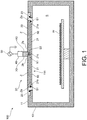
- a plasma treatment apparatus 100 of the embodiment is an apparatus that operates by a so-called inductively coupled plasma (ICP) method and generates discharge plasma using an electromagnetic field generated by causing a high frequency current to flow to an inductively coupling antenna unit 20 (hereinafter, simply referred to as antenna unit 20).
- ICP inductively coupled plasma
- the plasma treatment apparatus 100 includes a vacuum chamber 10 that accommodates a treatment target W, the antenna unit 20 that generates plasma in an internal space S of the vacuum chamber 10, a high frequency power source 30 that supplies high frequency power to the antenna unit 20, and the like.
- the internal space S of the vacuum chamber 10 is maintained at a predetermined degree of vacuum by a vacuum exhaust unit and a gas introducing unit (not illustrated).
- a mixed gas of argon and hydrogen is introduced at a predetermined pressure (for example, 1 Pa), and the high frequency power is supplied to the antenna unit 20 from the high frequency power source 30 via a matching box 40, thereby causing discharge plasma to be excited.
- the vacuum chamber 10 has an opening 111 formed in a wall surface thereof.
- the opening 111 having, for example, a rectangular shape when viewed from above is formed in a top wall portion 11 of the vacuum chamber 10.
- a lid 22 is detachably arranged at the opening 111, and the opening 111 is blocked with the lid 22, thereby sealing the internal space S.
- the antenna unit 20 has a configuration in which one or a plurality of antenna conductors 21 are attached to the lid 22 and, here, further includes a frame 23 that supports an outer peripheral portion of the lid 22. Besides, the antenna conductor 21, the lid 22, and the frame 23 are integrally installed at the opening 111 described above. Moreover, the antenna unit 20 of the embodiment includes one antenna conductor 21. However, the antenna unit may include a plurality of antenna conductors 21 connected in series or in parallel. In addition, the periphery of the opening 111 of the top wall portion 11 may have the same function as that of the frame 23.
- the antenna conductors 21 are fed with the high frequency power of 13.56 MHz and, here, are arranged to be parallel to each other at predetermined intervals.
- the antenna conductor 21 has a linear shape with a length of, for example, 500 mm or longer and has a width dimension of, for example, about 10 mm to 30 mm.
- the lid 22 has a length dimension longer than that of the antenna conductor 21 in a longitudinal direction of the lid and is supported by the frame 23 via a seal member S1.
- the lid 22 has a shape of a flat plate and is an insulating lid made of ceramics such as alumina, for example.
- the lid 22 may be a lid made of an organic material such as PEEK resin or fluororesin which has heat resistance.
- the antenna conductor 21 described above is attached to the lid 22 without a gap therebetween.
- the antenna conductor 21 is arranged to be in contact with a lower surface of the lid 22, and both end portions 21a and 21b of the antenna conductor are connected to the frame 23 and are grounded via the frame 23.
- a contamination preventive plate 60 such as a quartz plate is arranged under the antenna conductor 21, and the contamination preventive plate prevents the antenna conductor 21 from being contaminated with by-products such as dust produced in the vacuum chamber 10.
- the lid 22 separates the internal space S of the vacuum chamber 10, which is maintained at a predetermined degree of vacuum, from the atmosphere outside the vacuum chamber 10, a relatively thin plate can be used as the contamination preventive plate 60.
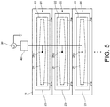
- the antenna units 20 are installed at the plurality of openings 111 formed in the top wall portion 11 of the vacuum chamber 10, and the antenna conductors 21 are attached to the respective lids 22 without a gap therebetween, the lids covering the respective openings 111.
- the openings 111 may have a width by which the lid 22 is attachable and detachable, and thus the width dimension thereof is, for example, 40 mm or wider and 150 mm or narrower and preferably 100 mm or narrower.
- the plurality of openings 111 is formed corresponding to the respective antenna units 20, and thereby a size of the openings 111 can be reduced.
- mechanical strength required by the lids 22 that cover the respective openings 111 is reduced. Consequently, a thickness of the lid 22 can be reduced, and the lid 22 here has a thickness of 5 mm or larger and 10 mm or smaller, for example.
- a feeding terminal X1 is connected to the antenna conductor 21.
- a through-hole is formed in the lid 22, and the feeding terminal X1 is inserted and, for example, brazed into the through-hole via a seal member S2.
- the through-hole is formed at a central portion 21c of the antenna conductor 21 in a longitudinal direction thereof, and thereby the feeding terminal X1 is electrically connected to the central portion 21c of the antenna conductor 21 in the longitudinal direction thereof.
- the high frequency power is supplied from the common high frequency power source 30 to the antenna conductors 21 that configure the respective antenna units 20, and here the high frequency power is supplied to the central portion 21c of the antenna conductor 21 in the longitudinal direction thereof.
- both end portions 21a and 21b of the antenna conductor 21 in the longitudinal direction thereof are supported by the frame 23 and are electrically connected to the frame 23.
- the frame 23 is a conductive member made of a stainless steel material, an aluminium material, or the like and is electrically connected to a wall surface of the vacuum chamber 10. Consequently, both end portions 21a and 21b of the antenna conductor 21 in the longitudinal direction thereof are grounded. Moreover, both end portions 21a and 21b of the antenna conductor 21 in the longitudinal direction thereof may be grounded via a capacitor.
- the plasma treatment apparatus 100 of the embodiment further includes a conductive member Z arranged to be substantially parallel to the antenna conductor 21 on a surface of the lid 22, the surface being opposite to a surface of the lid 22 to which the antenna conductor 21 is attached.
- the conductive member Z is arranged along the longitudinal direction of the antenna conductor 21, one end portion Za is electrically connected to the frame 23, and the other end portion Zb is connected to a ground terminal X2 of the matching box 40, for example.
- the high frequency current supplied to the central portion 21c of the antenna conductor 21 in the longitudinal direction thereof flows to the one end portion 21a or the other end portion 21b of the antenna conductor 21, then flows into the one end portion Za of the conductive member Z through the frame 23, and flows to the other end portion Zb of the conductive member Z. Consequently, the direction of the high frequency current flowing in the antenna conductor 21 is opposite to a direction of the high frequency current flowing in the conductive member Z.
- the antenna conductor 21, the frame 23, and the conductive member Z configure a reciprocating circuit with respect to the high frequency current supplied to the central portion 21c of the antenna conductor 21 in the longitudinal direction thereof. In the reciprocating circuit, a mutual inductance is generated between reciprocating antenna conductors, and an effect of cancelling and decreasing impedance of the antenna conductor against the high frequency current by an amount of the mutual inductance is achieved.
- the antenna conductor 21 is attached to the lid 22 without a gap therebetween, a gap where discharge may occur or plasma caused by the discharge is generated is not formed between the antenna conductor 21 and the lid 22, and the lid 22 or the like can be prevented from being contaminated.
- the lid 22 is made of ceramics, the lid 22 separates the internal space S of the vacuum chamber 10, which is maintained at the predetermined degree of vacuum, from the atmosphere outside the vacuum chamber 10, the mechanical strength of the lid 22 can be ensured.
- the openings 111 are formed in the top wall portion 11 of the vacuum chamber 10 corresponding to the respective antenna units 20, the size of the openings 111 can be reduced. Consequently, since the mechanical strength required by the lid 22 that covers each of the openings 111 is reduced, the thickness of the lid 22 can be reduced, and a reduction in manufacturing cost is achieved.
- the reciprocating circuit is configured using the conductive member Z, and the direction of the high frequency current flowing in the antenna conductor 21 is opposite to a direction of the high frequency current flowing in the conductive member Z.
- the impedance of the antenna conductor is cancelled by the amount of the mutual inductance generated by that the high frequency current flows to the antenna conductor 21 or the conductive member Z.
- the mutual inductance of the reciprocating circuit is inversely proportional to the thickness of the lid 22, the lid 22 can be thinned to a thickness of, for example, 5 mm to 10 mm, and thus impedance with respect to the high frequency current can be further decreased. Consequently, an increase in impedance due to elongation of the antenna conductor 21 can be suppressed, and an elongated antenna unit can be put to practical use.
- the antenna conductor 21 may be formed on a surface of the lid 22 by a metallization method.
- the lid 22 made of alumina or the like is processed to form a hole for the feeding terminal X1 and a hole for the ground terminal X2 of the matching box 40.
- Mo-Mn paste is applied to an electrode forming portion (antenna conductor or hole for an electrode terminal) on the surface of the lid 22 and is burned, and thereby a metal layer is formed.
- Ni plating or the like is performed on the metal layer, and the antenna conductor 21 having a thickness of, for example, about 30 ⁇ m to 40 ⁇ m is formed by silver brazing or the like.
- a Kovar pin having a coefficient of thermal expansion approximate to that of the alumina lid 22 is inserted into the hole for the terminal used as the feeding terminal X1 or the ground terminal X2 and, and an electrode terminal is brazed using silver brazing or the like.
- the antenna conductor 21 can be attached to the lid 22 without a gap therebetween, but heat generated in the antenna conductor can also be dissipated to the lid.
- the hole for the feeding terminal is formed at a central portion of the lid 22 in a longitudinal direction thereof, and the holes for the ground terminal are formed at both sides of the lid 22.
- a reciprocating circuit with respect to the high frequency power can be formed by metal films formed on an upper surface and a lower surface of the lid 22.
- the shape of the antenna conductor 21 is not limited to the linear shape as described in the above embodiment; for example, the antenna conductor 21 may have a shape in which the width dimension varies between the central portion in the longitudinal direction of the antenna conductor and both end portions in the longitudinal direction thereof, specifically, as illustrated in FIG. 5 , the antenna conductor may have a shape in which the width dimension is gradually reduced from the central portion 21c toward the one end portion 21a and the other end portion 21b in the longitudinal direction.
- Inductance of a parallel plate-type reciprocating antenna conductors is proportional to a length and an interval of the reciprocating antenna conductors and is inversely proportional to a width thereof.
- the inductance decreases, and when the reciprocating antenna conductors are separated from each other, the inductance increases.
- the inductance at the central portion can be decreased, and the inductance at both end portions can be increased.
- a high frequency power of 13.56 MHz is used as the high frequency power; however, the high frequency is not limited thereto, and a frequency of 30 kHz to 30 MHz can be applied as the high frequency power.
- An installation location of the antenna unit 20 is not limited to the top wall portion 11 of the vacuum chamber 10, and the antenna unit may be installed, for example, on a side wall or a bottom wall of the vacuum chamber 10 according to the form of the plasma treatment apparatus 100. Moreover, when the antenna unit 20 is installed on the side wall of the vacuum chamber 10, the plasma treatment can be performed while the treatment target W is transported along an up-down direction (vertical direction).
- a plasma treatment apparatus includes a vacuum chamber that accommodates a treatment target; an inductively coupling antenna unit that generates plasma in the vacuum chamber; and a high frequency power source that supplies a high frequency power to the inductively coupling antenna unit.
- the inductively coupling antenna unit has one or a plurality of antenna conductors and a lid that covers an opening formed in a wall surface of the vacuum chamber. The one or plurality of antenna conductors is attached to the lid without a gap in which discharge occurs.
- the plasma treatment apparatus having the configuration described above, since the one or plurality of antenna conductors is attached to the lid without a gap therebetween, plasma is not generated between the antenna conductor and the lid, and contamination inside the vacuum chamber can be prevented.
- a plurality of openings is formed to be substantially parallel to each other in the wall surface of the vacuum chamber, and the inductively coupling antenna unit is installed in each of the openings.
- each of the openings is reduced, and thereby the plurality of inductively coupling antenna units can be closely disposed. Consequently, a difference in length can be suppressed from occurring in a current path such as a power distribution line that connects the common high frequency power source and the respective antenna conductors.
- the high frequency power may be supplied to the plurality of inductively coupling antenna units from the common high frequency power source via a matching box.
- the plurality of inductively coupling antenna units is closely disposed, and thereby a difference in length can be suppressed from occurring in the current path such as the distribution line that connects the common high frequency power source and the respective inductively coupling antenna units, and a difference in current flowing to the plurality of antenna conductors can be suppressed. Further, a reduction in manufacturing cost with the common high frequency power source can be achieved.
- the lid In order for the lid to have mechanical strength necessary for separating vacuum in the vacuum chamber from an outside (atmosphere) of the vacuum chamber even though the thickness of the lid is reduced, the lid may be made of ceramics or an organic material.
- a feeding terminal of the high frequency power is connected to a central portion of the antenna conductor in a longitudinal direction thereof, and both end portions of the antenna conductor in the longitudinal direction thereof are grounded, and the high frequency power is supplied to the central portion of the antenna conductor in the longitudinal direction thereof via the feeding terminal.
- impedance can be substantially decreased by a half compared with a configuration in which the high frequency power is supplied to one end portion of the antenna conductor in the longitudinal direction so as to be introduced to the other end portion in the longitudinal direction, and elongation of the antenna conductor is achieved.
- the inductively coupling antenna unit further includes a frame that supports an outer peripheral portion of the lid, and a conductive member arranged to be substantially parallel to the antenna conductor on a surface of the lid, the surface being opposite to a surface of the lid to which the antenna conductor is attached. End portions of the antenna conductor in the longitudinal direction thereof are electrically connected to the frame, one end portion of the conductive member is electrically connected to the frame, and the other end portion of the conductive member is connected to a ground terminal of a matching box.
- the antenna conductor, the frame, and the conductive member configure a reciprocating circuit with respect to the high frequency power supplied to the central portion of the antenna conductor in the longitudinal direction thereof.
- a width of the antenna conductor or/and the conductive member is different at a central portion in a longitudinal direction thereof and at both end portions in the longitudinal direction thereof.
- inductance of the antenna conductor changes along the longitudinal direction of the antenna conductor, and thereby density of the plasma generated in the longitudinal direction of the antenna conductor can be equalized.
- the antenna conductor or/and the conductive member is/are formed on a surface of the lid by a metallization process.
- the antenna conductor or/and the conductive member is/are simply formed, and attachment/detachment or maintenance is easily performed.
- plasma is prevented from being generated between the antenna conductor and the lid, and contamination inside the vacuum chamber can be prevented.
- a reciprocating circuit is formed by the antenna conductor and the conductive member, and thereby inductance can be reduced and an elongated antenna unit can be put to practical use.
Landscapes
- Physics & Mathematics (AREA)
- Engineering & Computer Science (AREA)
- Plasma & Fusion (AREA)
- Chemical & Material Sciences (AREA)
- Analytical Chemistry (AREA)
- Electromagnetism (AREA)
- Spectroscopy & Molecular Physics (AREA)
- Plasma Technology (AREA)
- Drying Of Semiconductors (AREA)
Applications Claiming Priority (1)
| Application Number | Priority Date | Filing Date | Title |
|---|---|---|---|
| JP2018179418A JP6708887B2 (ja) | 2018-09-25 | 2018-09-25 | プラズマ処理装置、アンテナ導体又は/及び導電性部材の製造方法 |
Publications (2)
| Publication Number | Publication Date |
|---|---|
| EP3629362A1 true EP3629362A1 (de) | 2020-04-01 |
| EP3629362B1 EP3629362B1 (de) | 2021-04-07 |
Family
ID=67998120
Family Applications (1)
| Application Number | Title | Priority Date | Filing Date |
|---|---|---|---|
| EP19198319.6A Active EP3629362B1 (de) | 2018-09-25 | 2019-09-19 | Plasmabehandlungsvorrichtung und ansteuerungsverfahren dafür |
Country Status (5)
| Country | Link |
|---|---|
| US (1) | US11164728B2 (de) |
| EP (1) | EP3629362B1 (de) |
| JP (1) | JP6708887B2 (de) |
| KR (1) | KR102200085B1 (de) |
| CN (1) | CN110944443B (de) |
Cited By (1)
| Publication number | Priority date | Publication date | Assignee | Title |
|---|---|---|---|---|
| TWI847901B (zh) * | 2022-12-13 | 2024-07-01 | 日商日新電機股份有限公司 | 電漿處理裝置 |
Citations (6)
| Publication number | Priority date | Publication date | Assignee | Title |
|---|---|---|---|---|
| US20020038791A1 (en) * | 2000-10-03 | 2002-04-04 | Tomohiro Okumura | Plasma processing method and apparatus |
| JP2012049065A (ja) * | 2010-08-30 | 2012-03-08 | Nissin Electric Co Ltd | プラズマ処理装置 |
| EP2538432A2 (de) * | 2011-06-24 | 2012-12-26 | Nissin Electric Co., Ltd. | Vorrichtung zur Plasmaverarbeitung |
| JP2013020871A (ja) * | 2011-07-13 | 2013-01-31 | Nissin Electric Co Ltd | プラズマ処理装置 |
| JP2017224789A (ja) * | 2016-06-17 | 2017-12-21 | 東京エレクトロン株式会社 | 成膜方法およびtftの製造方法 |
| JP2018101463A (ja) | 2016-12-19 | 2018-06-28 | 株式会社プラズマイオンアシスト | 誘導結合型アンテナユニット及びプラズマ処理装置 |
Family Cites Families (9)
| Publication number | Priority date | Publication date | Assignee | Title |
|---|---|---|---|---|
| US20040261718A1 (en) * | 2003-06-26 | 2004-12-30 | Kim Nam Hun | Plasma source coil for generating plasma and plasma chamber using the same |
| JP4694596B2 (ja) * | 2008-06-18 | 2011-06-08 | 東京エレクトロン株式会社 | マイクロ波プラズマ処理装置及びマイクロ波の給電方法 |
| JP4621287B2 (ja) * | 2009-03-11 | 2011-01-26 | 株式会社イー・エム・ディー | プラズマ処理装置 |
| JP5400434B2 (ja) * | 2009-03-11 | 2014-01-29 | 株式会社イー・エム・ディー | プラズマ処理装置 |
| EP2546385A4 (de) * | 2010-03-09 | 2013-08-07 | Emd Corp | Sputtervorrichtung |
| US20140150975A1 (en) * | 2010-09-06 | 2014-06-05 | Emd Corporation | Plasma processing device |
| JP5462369B2 (ja) | 2010-09-10 | 2014-04-02 | 株式会社イー・エム・ディー | プラズマ処理装置 |
| JP5018994B1 (ja) | 2011-11-09 | 2012-09-05 | 日新電機株式会社 | プラズマ処理装置 |
| JP2013134835A (ja) * | 2011-12-26 | 2013-07-08 | Nissin Electric Co Ltd | プラズマ処理装置 |
-
2018
- 2018-09-25 JP JP2018179418A patent/JP6708887B2/ja active Active
-
2019
- 2019-09-19 EP EP19198319.6A patent/EP3629362B1/de active Active
- 2019-09-24 US US16/579,874 patent/US11164728B2/en active Active
- 2019-09-24 CN CN201910907010.6A patent/CN110944443B/zh active Active
- 2019-09-24 KR KR1020190117336A patent/KR102200085B1/ko not_active Expired - Fee Related
Patent Citations (6)
| Publication number | Priority date | Publication date | Assignee | Title |
|---|---|---|---|---|
| US20020038791A1 (en) * | 2000-10-03 | 2002-04-04 | Tomohiro Okumura | Plasma processing method and apparatus |
| JP2012049065A (ja) * | 2010-08-30 | 2012-03-08 | Nissin Electric Co Ltd | プラズマ処理装置 |
| EP2538432A2 (de) * | 2011-06-24 | 2012-12-26 | Nissin Electric Co., Ltd. | Vorrichtung zur Plasmaverarbeitung |
| JP2013020871A (ja) * | 2011-07-13 | 2013-01-31 | Nissin Electric Co Ltd | プラズマ処理装置 |
| JP2017224789A (ja) * | 2016-06-17 | 2017-12-21 | 東京エレクトロン株式会社 | 成膜方法およびtftの製造方法 |
| JP2018101463A (ja) | 2016-12-19 | 2018-06-28 | 株式会社プラズマイオンアシスト | 誘導結合型アンテナユニット及びプラズマ処理装置 |
Cited By (1)
| Publication number | Priority date | Publication date | Assignee | Title |
|---|---|---|---|---|
| TWI847901B (zh) * | 2022-12-13 | 2024-07-01 | 日商日新電機股份有限公司 | 電漿處理裝置 |
Also Published As
| Publication number | Publication date |
|---|---|
| EP3629362B1 (de) | 2021-04-07 |
| KR102200085B1 (ko) | 2021-01-08 |
| JP2020053169A (ja) | 2020-04-02 |
| CN110944443B (zh) | 2023-07-07 |
| KR20200035226A (ko) | 2020-04-02 |
| US11164728B2 (en) | 2021-11-02 |
| US20200098548A1 (en) | 2020-03-26 |
| CN110944443A (zh) | 2020-03-31 |
| JP6708887B2 (ja) | 2020-06-10 |
Similar Documents
| Publication | Publication Date | Title |
|---|---|---|
| US12205843B2 (en) | Ground electrode formed in an electrostatic chuck for a plasma processing chamber | |
| US12020912B2 (en) | Integrated electrode and ground plane for a substrate support | |
| KR101263109B1 (ko) | 플라즈마 처리 장치 및 그 유전체창 구조 | |
| KR100756095B1 (ko) | 처리가스도입기구 및 플라즈마처리장치 | |
| KR101812920B1 (ko) | 플라즈마 처리 장치 | |
| US20130286532A1 (en) | Semiconductor manufacturing apparatus member | |
| EP2615889A1 (de) | Plasmaverarbeitungsvorrichtung | |
| JP7836736B2 (ja) | プラズマ処理装置 | |
| US20160118284A1 (en) | Plasma processing apparatus | |
| US20120138450A1 (en) | Immersible Plasma Coil Assembly and Method for Operating the Same | |
| EP3629362B1 (de) | Plasmabehandlungsvorrichtung und ansteuerungsverfahren dafür | |
| US20180019099A1 (en) | Plasma processing apparatus | |
| JP6418543B2 (ja) | プラズマ処理装置及びプラズマ処理装置用アンテナユニット | |
| EP1314694A2 (de) | Ozonerzeuger | |
| JP4788504B2 (ja) | プラズマ処理装置の給電構造 | |
| JP4705967B2 (ja) | プラズマ処理装置 | |
| JP7214843B2 (ja) | セラミックヒータ | |
| JP7202641B2 (ja) | プラズマ処理装置およびプラズマ処理方法 | |
| KR102786708B1 (ko) | 체결 구조와 체결 방법 및 플라즈마 처리 장치 | |
| JP4765648B2 (ja) | マイクロプラズマジェット発生装置 | |
| CN114566414A (zh) | 真空装置 | |
| JP6465948B1 (ja) | 基板処理装置及び成膜装置 | |
| US20210343501A1 (en) | Plasma processing apparatus and plasma processing method | |
| JP6304550B2 (ja) | プラズマ処理装置 | |
| CN116998225A (zh) | 等离子体处理装置 |
Legal Events
| Date | Code | Title | Description |
|---|---|---|---|
| PUAI | Public reference made under article 153(3) epc to a published international application that has entered the european phase |
Free format text: ORIGINAL CODE: 0009012 |
|
| STAA | Information on the status of an ep patent application or granted ep patent |
Free format text: STATUS: REQUEST FOR EXAMINATION WAS MADE |
|
| 17P | Request for examination filed |
Effective date: 20191002 |
|
| AK | Designated contracting states |
Kind code of ref document: A1 Designated state(s): AL AT BE BG CH CY CZ DE DK EE ES FI FR GB GR HR HU IE IS IT LI LT LU LV MC MK MT NL NO PL PT RO RS SE SI SK SM TR |
|
| AX | Request for extension of the european patent |
Extension state: BA ME |
|
| GRAP | Despatch of communication of intention to grant a patent |
Free format text: ORIGINAL CODE: EPIDOSNIGR1 |
|
| STAA | Information on the status of an ep patent application or granted ep patent |
Free format text: STATUS: GRANT OF PATENT IS INTENDED |
|
| INTG | Intention to grant announced |
Effective date: 20201106 |
|
| GRAS | Grant fee paid |
Free format text: ORIGINAL CODE: EPIDOSNIGR3 |
|
| GRAA | (expected) grant |
Free format text: ORIGINAL CODE: 0009210 |
|
| STAA | Information on the status of an ep patent application or granted ep patent |
Free format text: STATUS: THE PATENT HAS BEEN GRANTED |
|
| AK | Designated contracting states |
Kind code of ref document: B1 Designated state(s): AL AT BE BG CH CY CZ DE DK EE ES FI FR GB GR HR HU IE IS IT LI LT LU LV MC MK MT NL NO PL PT RO RS SE SI SK SM TR |
|
| REG | Reference to a national code |
Ref country code: GB Ref legal event code: FG4D |
|
| REG | Reference to a national code |
Ref country code: AT Ref legal event code: REF Ref document number: 1380780 Country of ref document: AT Kind code of ref document: T Effective date: 20210415 Ref country code: CH Ref legal event code: EP |
|
| REG | Reference to a national code |
Ref country code: DE Ref legal event code: R096 Ref document number: 602019003762 Country of ref document: DE |
|
| REG | Reference to a national code |
Ref country code: IE Ref legal event code: FG4D |
|
| REG | Reference to a national code |
Ref country code: SE Ref legal event code: TRGR |
|
| REG | Reference to a national code |
Ref country code: LT Ref legal event code: MG9D |
|
| REG | Reference to a national code |
Ref country code: NL Ref legal event code: MP Effective date: 20210407 Ref country code: AT Ref legal event code: MK05 Ref document number: 1380780 Country of ref document: AT Kind code of ref document: T Effective date: 20210407 |
|
| PG25 | Lapsed in a contracting state [announced via postgrant information from national office to epo] |
Ref country code: AT Free format text: LAPSE BECAUSE OF FAILURE TO SUBMIT A TRANSLATION OF THE DESCRIPTION OR TO PAY THE FEE WITHIN THE PRESCRIBED TIME-LIMIT Effective date: 20210407 Ref country code: BG Free format text: LAPSE BECAUSE OF FAILURE TO SUBMIT A TRANSLATION OF THE DESCRIPTION OR TO PAY THE FEE WITHIN THE PRESCRIBED TIME-LIMIT Effective date: 20210707 Ref country code: NL Free format text: LAPSE BECAUSE OF FAILURE TO SUBMIT A TRANSLATION OF THE DESCRIPTION OR TO PAY THE FEE WITHIN THE PRESCRIBED TIME-LIMIT Effective date: 20210407 Ref country code: HR Free format text: LAPSE BECAUSE OF FAILURE TO SUBMIT A TRANSLATION OF THE DESCRIPTION OR TO PAY THE FEE WITHIN THE PRESCRIBED TIME-LIMIT Effective date: 20210407 Ref country code: LT Free format text: LAPSE BECAUSE OF FAILURE TO SUBMIT A TRANSLATION OF THE DESCRIPTION OR TO PAY THE FEE WITHIN THE PRESCRIBED TIME-LIMIT Effective date: 20210407 Ref country code: FI Free format text: LAPSE BECAUSE OF FAILURE TO SUBMIT A TRANSLATION OF THE DESCRIPTION OR TO PAY THE FEE WITHIN THE PRESCRIBED TIME-LIMIT Effective date: 20210407 |
|
| PG25 | Lapsed in a contracting state [announced via postgrant information from national office to epo] |
Ref country code: IS Free format text: LAPSE BECAUSE OF FAILURE TO SUBMIT A TRANSLATION OF THE DESCRIPTION OR TO PAY THE FEE WITHIN THE PRESCRIBED TIME-LIMIT Effective date: 20210807 Ref country code: GR Free format text: LAPSE BECAUSE OF FAILURE TO SUBMIT A TRANSLATION OF THE DESCRIPTION OR TO PAY THE FEE WITHIN THE PRESCRIBED TIME-LIMIT Effective date: 20210708 Ref country code: NO Free format text: LAPSE BECAUSE OF FAILURE TO SUBMIT A TRANSLATION OF THE DESCRIPTION OR TO PAY THE FEE WITHIN THE PRESCRIBED TIME-LIMIT Effective date: 20210707 Ref country code: PL Free format text: LAPSE BECAUSE OF FAILURE TO SUBMIT A TRANSLATION OF THE DESCRIPTION OR TO PAY THE FEE WITHIN THE PRESCRIBED TIME-LIMIT Effective date: 20210407 Ref country code: LV Free format text: LAPSE BECAUSE OF FAILURE TO SUBMIT A TRANSLATION OF THE DESCRIPTION OR TO PAY THE FEE WITHIN THE PRESCRIBED TIME-LIMIT Effective date: 20210407 Ref country code: RS Free format text: LAPSE BECAUSE OF FAILURE TO SUBMIT A TRANSLATION OF THE DESCRIPTION OR TO PAY THE FEE WITHIN THE PRESCRIBED TIME-LIMIT Effective date: 20210407 Ref country code: PT Free format text: LAPSE BECAUSE OF FAILURE TO SUBMIT A TRANSLATION OF THE DESCRIPTION OR TO PAY THE FEE WITHIN THE PRESCRIBED TIME-LIMIT Effective date: 20210809 |
|
| REG | Reference to a national code |
Ref country code: DE Ref legal event code: R097 Ref document number: 602019003762 Country of ref document: DE |
|
| PG25 | Lapsed in a contracting state [announced via postgrant information from national office to epo] |
Ref country code: EE Free format text: LAPSE BECAUSE OF FAILURE TO SUBMIT A TRANSLATION OF THE DESCRIPTION OR TO PAY THE FEE WITHIN THE PRESCRIBED TIME-LIMIT Effective date: 20210407 Ref country code: ES Free format text: LAPSE BECAUSE OF FAILURE TO SUBMIT A TRANSLATION OF THE DESCRIPTION OR TO PAY THE FEE WITHIN THE PRESCRIBED TIME-LIMIT Effective date: 20210407 Ref country code: SK Free format text: LAPSE BECAUSE OF FAILURE TO SUBMIT A TRANSLATION OF THE DESCRIPTION OR TO PAY THE FEE WITHIN THE PRESCRIBED TIME-LIMIT Effective date: 20210407 Ref country code: SM Free format text: LAPSE BECAUSE OF FAILURE TO SUBMIT A TRANSLATION OF THE DESCRIPTION OR TO PAY THE FEE WITHIN THE PRESCRIBED TIME-LIMIT Effective date: 20210407 Ref country code: RO Free format text: LAPSE BECAUSE OF FAILURE TO SUBMIT A TRANSLATION OF THE DESCRIPTION OR TO PAY THE FEE WITHIN THE PRESCRIBED TIME-LIMIT Effective date: 20210407 Ref country code: CZ Free format text: LAPSE BECAUSE OF FAILURE TO SUBMIT A TRANSLATION OF THE DESCRIPTION OR TO PAY THE FEE WITHIN THE PRESCRIBED TIME-LIMIT Effective date: 20210407 Ref country code: DK Free format text: LAPSE BECAUSE OF FAILURE TO SUBMIT A TRANSLATION OF THE DESCRIPTION OR TO PAY THE FEE WITHIN THE PRESCRIBED TIME-LIMIT Effective date: 20210407 |
|
| PLBE | No opposition filed within time limit |
Free format text: ORIGINAL CODE: 0009261 |
|
| STAA | Information on the status of an ep patent application or granted ep patent |
Free format text: STATUS: NO OPPOSITION FILED WITHIN TIME LIMIT |
|
| 26N | No opposition filed |
Effective date: 20220110 |
|
| REG | Reference to a national code |
Ref country code: BE Ref legal event code: MM Effective date: 20210930 |
|
| PG25 | Lapsed in a contracting state [announced via postgrant information from national office to epo] |
Ref country code: IS Free format text: LAPSE BECAUSE OF FAILURE TO SUBMIT A TRANSLATION OF THE DESCRIPTION OR TO PAY THE FEE WITHIN THE PRESCRIBED TIME-LIMIT Effective date: 20210807 Ref country code: MC Free format text: LAPSE BECAUSE OF FAILURE TO SUBMIT A TRANSLATION OF THE DESCRIPTION OR TO PAY THE FEE WITHIN THE PRESCRIBED TIME-LIMIT Effective date: 20210407 Ref country code: AL Free format text: LAPSE BECAUSE OF FAILURE TO SUBMIT A TRANSLATION OF THE DESCRIPTION OR TO PAY THE FEE WITHIN THE PRESCRIBED TIME-LIMIT Effective date: 20210407 |
|
| PG25 | Lapsed in a contracting state [announced via postgrant information from national office to epo] |
Ref country code: LU Free format text: LAPSE BECAUSE OF NON-PAYMENT OF DUE FEES Effective date: 20210919 Ref country code: IT Free format text: LAPSE BECAUSE OF FAILURE TO SUBMIT A TRANSLATION OF THE DESCRIPTION OR TO PAY THE FEE WITHIN THE PRESCRIBED TIME-LIMIT Effective date: 20210407 Ref country code: IE Free format text: LAPSE BECAUSE OF NON-PAYMENT OF DUE FEES Effective date: 20210919 Ref country code: BE Free format text: LAPSE BECAUSE OF NON-PAYMENT OF DUE FEES Effective date: 20210930 |
|
| REG | Reference to a national code |
Ref country code: CH Ref legal event code: PL |
|
| PG25 | Lapsed in a contracting state [announced via postgrant information from national office to epo] |
Ref country code: CY Free format text: LAPSE BECAUSE OF FAILURE TO SUBMIT A TRANSLATION OF THE DESCRIPTION OR TO PAY THE FEE WITHIN THE PRESCRIBED TIME-LIMIT Effective date: 20210407 |
|
| PG25 | Lapsed in a contracting state [announced via postgrant information from national office to epo] |
Ref country code: LI Free format text: LAPSE BECAUSE OF NON-PAYMENT OF DUE FEES Effective date: 20220930 Ref country code: HU Free format text: LAPSE BECAUSE OF FAILURE TO SUBMIT A TRANSLATION OF THE DESCRIPTION OR TO PAY THE FEE WITHIN THE PRESCRIBED TIME-LIMIT; INVALID AB INITIO Effective date: 20190919 Ref country code: CH Free format text: LAPSE BECAUSE OF NON-PAYMENT OF DUE FEES Effective date: 20220930 |
|
| PG25 | Lapsed in a contracting state [announced via postgrant information from national office to epo] |
Ref country code: MK Free format text: LAPSE BECAUSE OF FAILURE TO SUBMIT A TRANSLATION OF THE DESCRIPTION OR TO PAY THE FEE WITHIN THE PRESCRIBED TIME-LIMIT Effective date: 20210407 |
|
| GBPC | Gb: european patent ceased through non-payment of renewal fee |
Effective date: 20230919 |
|
| PG25 | Lapsed in a contracting state [announced via postgrant information from national office to epo] |
Ref country code: TR Free format text: LAPSE BECAUSE OF FAILURE TO SUBMIT A TRANSLATION OF THE DESCRIPTION OR TO PAY THE FEE WITHIN THE PRESCRIBED TIME-LIMIT Effective date: 20210407 |
|
| PG25 | Lapsed in a contracting state [announced via postgrant information from national office to epo] |
Ref country code: GB Free format text: LAPSE BECAUSE OF NON-PAYMENT OF DUE FEES Effective date: 20230919 |
|
| PG25 | Lapsed in a contracting state [announced via postgrant information from national office to epo] |
Ref country code: GB Free format text: LAPSE BECAUSE OF NON-PAYMENT OF DUE FEES Effective date: 20230919 |
|
| PG25 | Lapsed in a contracting state [announced via postgrant information from national office to epo] |
Ref country code: MT Free format text: LAPSE BECAUSE OF FAILURE TO SUBMIT A TRANSLATION OF THE DESCRIPTION OR TO PAY THE FEE WITHIN THE PRESCRIBED TIME-LIMIT Effective date: 20210407 |
|
| PGFP | Annual fee paid to national office [announced via postgrant information from national office to epo] |
Ref country code: FR Payment date: 20240924 Year of fee payment: 6 |
|
| PGFP | Annual fee paid to national office [announced via postgrant information from national office to epo] |
Ref country code: DE Payment date: 20250915 Year of fee payment: 7 |
|
| PGFP | Annual fee paid to national office [announced via postgrant information from national office to epo] |
Ref country code: SE Payment date: 20250922 Year of fee payment: 7 |