EP3631299B1 - Halbleiterfilm und photozellenlichtdetektor - Google Patents
Halbleiterfilm und photozellenlichtdetektor Download PDFInfo
- Publication number
- EP3631299B1 EP3631299B1 EP18731682.3A EP18731682A EP3631299B1 EP 3631299 B1 EP3631299 B1 EP 3631299B1 EP 18731682 A EP18731682 A EP 18731682A EP 3631299 B1 EP3631299 B1 EP 3631299B1
- Authority
- EP
- European Patent Office
- Prior art keywords
- light
- semiconductor film
- detection system
- top electrode
- interdigital
- Prior art date
- Legal status (The legal status is an assumption and is not a legal conclusion. Google has not performed a legal analysis and makes no representation as to the accuracy of the status listed.)
- Active
Links
Images


Classifications
-
- G—PHYSICS
- G01—MEASURING; TESTING
- G01J—MEASUREMENT OF INTENSITY, VELOCITY, SPECTRAL CONTENT, POLARISATION, PHASE OR PULSE CHARACTERISTICS OF INFRARED, VISIBLE OR ULTRAVIOLET LIGHT; COLORIMETRY; RADIATION PYROMETRY
- G01J1/00—Photometry, e.g. photographic exposure meter
- G01J1/42—Photometry, e.g. photographic exposure meter using electric radiation detectors
- G01J1/429—Photometry, e.g. photographic exposure meter using electric radiation detectors applied to measurement of ultraviolet light
-
- G—PHYSICS
- G01—MEASURING; TESTING
- G01J—MEASUREMENT OF INTENSITY, VELOCITY, SPECTRAL CONTENT, POLARISATION, PHASE OR PULSE CHARACTERISTICS OF INFRARED, VISIBLE OR ULTRAVIOLET LIGHT; COLORIMETRY; RADIATION PYROMETRY
- G01J1/00—Photometry, e.g. photographic exposure meter
- G01J1/02—Details
- G01J1/08—Arrangements of light sources specially adapted for photometry standard sources, also using luminescent or radioactive material
-
- F—MECHANICAL ENGINEERING; LIGHTING; HEATING; WEAPONS; BLASTING
- F23—COMBUSTION APPARATUS; COMBUSTION PROCESSES
- F23N—REGULATING OR CONTROLLING COMBUSTION
- F23N5/00—Systems for controlling combustion
-
- F—MECHANICAL ENGINEERING; LIGHTING; HEATING; WEAPONS; BLASTING
- F23—COMBUSTION APPARATUS; COMBUSTION PROCESSES
- F23N—REGULATING OR CONTROLLING COMBUSTION
- F23N5/00—Systems for controlling combustion
- F23N5/02—Systems for controlling combustion using devices responsive to thermal changes or to thermal expansion of a medium
- F23N5/08—Systems for controlling combustion using devices responsive to thermal changes or to thermal expansion of a medium using light-sensitive elements
- F23N5/082—Systems for controlling combustion using devices responsive to thermal changes or to thermal expansion of a medium using light-sensitive elements using electronic means
-
- G—PHYSICS
- G01—MEASURING; TESTING
- G01J—MEASUREMENT OF INTENSITY, VELOCITY, SPECTRAL CONTENT, POLARISATION, PHASE OR PULSE CHARACTERISTICS OF INFRARED, VISIBLE OR ULTRAVIOLET LIGHT; COLORIMETRY; RADIATION PYROMETRY
- G01J1/00—Photometry, e.g. photographic exposure meter
- G01J1/42—Photometry, e.g. photographic exposure meter using electric radiation detectors
- G01J1/4228—Photometry, e.g. photographic exposure meter using electric radiation detectors arrangements with two or more detectors, e.g. for sensitivity compensation
-
- G—PHYSICS
- G01—MEASURING; TESTING
- G01J—MEASUREMENT OF INTENSITY, VELOCITY, SPECTRAL CONTENT, POLARISATION, PHASE OR PULSE CHARACTERISTICS OF INFRARED, VISIBLE OR ULTRAVIOLET LIGHT; COLORIMETRY; RADIATION PYROMETRY
- G01J1/00—Photometry, e.g. photographic exposure meter
- G01J1/42—Photometry, e.g. photographic exposure meter using electric radiation detectors
- G01J1/4257—Photometry, e.g. photographic exposure meter using electric radiation detectors applied to monitoring the characteristics of a beam, e.g. laser beam, headlamp beam
-
- G—PHYSICS
- G01—MEASURING; TESTING
- G01J—MEASUREMENT OF INTENSITY, VELOCITY, SPECTRAL CONTENT, POLARISATION, PHASE OR PULSE CHARACTERISTICS OF INFRARED, VISIBLE OR ULTRAVIOLET LIGHT; COLORIMETRY; RADIATION PYROMETRY
- G01J1/00—Photometry, e.g. photographic exposure meter
- G01J1/42—Photometry, e.g. photographic exposure meter using electric radiation detectors
- G01J1/44—Electric circuits
-
- G—PHYSICS
- G01—MEASURING; TESTING
- G01J—MEASUREMENT OF INTENSITY, VELOCITY, SPECTRAL CONTENT, POLARISATION, PHASE OR PULSE CHARACTERISTICS OF INFRARED, VISIBLE OR ULTRAVIOLET LIGHT; COLORIMETRY; RADIATION PYROMETRY
- G01J5/00—Radiation pyrometry, e.g. infrared or optical thermometry
- G01J5/0014—Radiation pyrometry, e.g. infrared or optical thermometry for sensing the radiation from gases, flames
- G01J5/0018—Flames, plasma or welding
-
- F—MECHANICAL ENGINEERING; LIGHTING; HEATING; WEAPONS; BLASTING
- F23—COMBUSTION APPARATUS; COMBUSTION PROCESSES
- F23M—CASINGS, LININGS, WALLS OR DOORS SPECIALLY ADAPTED FOR COMBUSTION CHAMBERS, e.g. FIREBRIDGES; DEVICES FOR DEFLECTING AIR, FLAMES OR COMBUSTION PRODUCTS IN COMBUSTION CHAMBERS; SAFETY ARRANGEMENTS SPECIALLY ADAPTED FOR COMBUSTION APPARATUS; DETAILS OF COMBUSTION CHAMBERS, NOT OTHERWISE PROVIDED FOR
- F23M2900/00—Special features of, or arrangements for combustion chambers
- F23M2900/11041—Means for observing or monitoring flames using photoelectric devices, e.g. phototransistors
-
- G—PHYSICS
- G01—MEASURING; TESTING
- G01J—MEASUREMENT OF INTENSITY, VELOCITY, SPECTRAL CONTENT, POLARISATION, PHASE OR PULSE CHARACTERISTICS OF INFRARED, VISIBLE OR ULTRAVIOLET LIGHT; COLORIMETRY; RADIATION PYROMETRY
- G01J1/00—Photometry, e.g. photographic exposure meter
- G01J1/42—Photometry, e.g. photographic exposure meter using electric radiation detectors
- G01J1/44—Electric circuits
- G01J2001/4446—Type of detector
Definitions
- the following description relates to semiconductor films and phototube light detectors and, more particularly, to a combination of a semiconductor film and a phototube light detector.
- UV flame detection requires a sharp wavelength cutoff so that incident sunlight will not trigger a false alarm.
- Phototubes based on applications of photoelectric effect can meet this requirement but require high voltages, are relatively high cost, fragile and oftentimes do not accurately quantify incident UV light intensity.
- solid state semiconductor film devices measure relative light intensities but suffer from limited sensitivity and selectivity. Thus, achieving a sufficiently sharp absorption cutoff at solar wavelengths to prevent false-positive alarms remains a challenge for certain sensor types.
- US 2008/042563 A1 discloses a photocathode, an electron tube, a field assist type photocathode, a field assist type photocathode array, and a field assist type electron tube.
- JP H0750149 A discloses a photocathode, a phototube and a photodetector, and more particularly means of obtaining one dimensional or two-dimensional information such as an incident position or an incident light image of weak light.
- JP H0896705 A discloses a semiconductor photocathode and a phototube which are formed by using a semiconductor as a constituent material in an image pickup tube or a photometric device and emit photoelectrons excited by receiving incident light.
- a light detection system for association with a light source, the light detection system comprising: a light detector comprising semiconductor film and phototube devices, the semiconductor film device comprising a photosensitive semiconductor film; the light detector being configured to be disposed with at least one line-of-sight (LOS) to the light source; and circuitry coupled to the light detector, the light detector and the circuitry being configured to cooperatively identify a presence and a characteristic of a light emission event at the light source; wherein the light detector comprises interdigital electrodes partially formed on the photosensitive semiconductor film and a top electrode opposite the interdigital electrodes, and wherein the interdigital electrodes are provided as a first interdigital electrode portion and a second interdigital electrode portion, the first interdigital electrode portion comprising first digital elements and the second interdigital electrode portion comprising second digital elements; and wherein the circuitry comprises: a processor; a first loop coupled at opposite ends thereof to the interdigital electrode and the top electrode, respectively, and to the processor, wherein the first loop
- the light source may be provided as a plurality of light sources and the light detector may be provided as one or more light detectors each being configured to be disposed with at least one respective LOSs to corresponding ones or more of the plurality of light sources.
- the characteristic of the light emission event may include a frequency of light produced by the light emission event.
- the light detector may include a first wafer having opposed first and second major surfaces; and a second wafer having opposed first and second major surfaces; wherein the photosensitive semiconductor film is disposed on the second major surface of the first wafer; wherein a plurality of interdigital electrodes (IDEs) are partially formed on the photosensitive semiconductor film; and wherein the top electrode is disposed on the first major surface of the second wafer.
- the first and second wafers may be bonded such that the respective second and first major surfaces of the first and second wafers face each other with a cavity defined between the respective second and first major surfaces of the first and second wafers.
- the cavity may be chargeable with gas supportive of photoelectric phenomena between the IDEs and the top electrode.
- the first and second wafers may each include at least one or more of silicon, oxide on silicon, quartz, sapphire, fused silica and ultraviolet (UV) transparent glass.
- the cavity may be hermetically sealed.
- the first and second wafers may be frit bonded, anodically bonded or glued.
- a distance between the IDEs and the top electrode may be anywhere from being similar to a pitch of the IDEs to being substantially larger than the pitch of the IDEs.
- Both of the IDEs and the top electrode may be metallic.
- the top electrode may have an IDE structure and the light detector may further include a photosensitive semiconductor film interposed between the IDE structure of the top electrode and the first major surface of the second wafer.
- a semiconductor film device and phototube are provided in combination with each other to form a single sensor.
- a photosensitive semiconductor film is deposited onto a wafer and interdigital electrode (IDE) patterning follows.
- Another wafer includes a top electrode and is bonded to the first wafer to form the sensor structure. This bonding is carried out in environment such that the sensor cavity between the two wafer surfaces is filled with an appropriate gas composition at suitable pressure to afford photoelectric phenomenon between top and IDE electrodes.
- One of the electrode structures is formed of metal, such as nickel (Ni) or gold (Au), with a work function that is suitable for deep ultraviolet (UV) responsivity.
- the top electrode contact may be fabricated in the form of an IDE structure and may include a photosensitive semiconductor film to further enhance sensor responsivity and functionality.
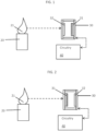
- the light detection system 10 includes at least one or more light sources 20, at least one or more light detectors 30 and circuitry 40.
- Each of the at least one light sources 20 may be provided as a flame producing element or a burner 21 or a pilot light for a water heater or a stovetop, for example, and may be provided as a single feature (see FIGS. 1 and 2 ) or as two or more features (see FIGS. 3, 4 and 5 ).
- Each of the at least one or more light detectors 30 includes a semiconductor film device 31 that is combined with a phototube 32 into a single sensor that is disposed to sense whether one or more of the light sources 20 are or are not actually producing, generating or emitting light and, if light is being produced, generated or emitted, to also sense a characteristic of that light. To this end, the at least one or more light detectors 30 are each disposed with at least one line-of-sight (LOS) to at least one corresponding light source 20.
- LOS line-of-sight
- the circuitry 40 is coupled to each of the at least one or more light detectors 30.
- the at least one or more light detectors 30 and the circuitry 40 are configured to cooperatively identify an occurrence or the presence and the characteristic of a light emission event (e.g., a flame at the burner 21) at the at least one corresponding light source 20.
- a light emission event e.g., a flame at the burner 21
- the light detection system 10 may be provided with a 1:1 ratio of one or more light sources 20 and one or more light detectors 30 (e.g., one light source 20 and one light detector 30 as shown in FIGS. 1 and 2 ), an N:1 ratio of one or more light sources 20 and one or more light detectors 30 (e.g., two light sources 20 and one light detector 30 as shown in FIGS. 3 and 4 ) or an N:N ratio of one or more light sources 20 and one or more light detectors 30 (e.g., one light source 20 and one light detector 30, two light sources 20 and two light detectors 30 as shown in FIGS. 5 and 6 , three light sources 20 and three light detectors 30, etc.).
- a 1:1 ratio of one or more light sources 20 and one or more light detectors 30 e.g., one light source 20 and one light detector 30 as shown in FIGS. 1 and 2
- an N:1 ratio of one or more light sources 20 and one or more light detectors 30 e.g., two light sources 20 and one light detector 30 as shown
- each one of the at least one or more light detectors 30 includes a first wafer 31 and a second wafer 32.
- the first and second wafers 31 and 32 may include silicon, oxide on silicon, quartz, sapphire, fused silica, UV transparent glass or other similar materials.
- at least one of the first and second wafers 31 and 32 are transparent to certain types of light, such as visible light, ultraviolet (UV) light, infrared (IR), etc. (e.g., the first wafer 31 may be formed of oxide on silicon, which is not transparent to UV light and the second wafer 32 would then have to be transparent to UV light).
- the first wafer 31 has a first major surface 310 and a second major surface 311 which opposes the first major surface 310.
- the second wafer 32 has a first major surface 320 and a second major surface 321 which opposes the first major surface 320.
- a photosensitive semiconductor film 33 is disposed on a portion of the second major surface 311 of the first wafer 31 and interdigital electrodes (IDEs) 34 are partially formed on the photosensitive semiconductor film 33.
- a top electrode 35 is disposed on a portion of the first major surface 320 of the second wafer 32.
- the first and second wafers 31 and 32 are bonded such that the second major surface 311 and the first major surface 320 face each other with a cavity 36 defined therebetween.
- This cavity 36 may be hermetically sealed (or otherwise sealed) and is thus chargeable with a gas that is supportive of photoelectric phenomena occurring between the IDEs 34 and the top electrode 35.
- the first and second wafers 31 and 32 may be frit bonded, anodically bonded or glued (e.g., thermosetting glue or UV curable glue) to one another.
- each one of the at least one or more light detectors 30 may further include spacers 37 or bulkheads which are structurally interposed between the first and second wafers 31 and 32 about and at a distance from respective perimeters of the photosensitive semiconductor film 33, the IDEs 34 and the top electrode 35. Adhesive can be applied to opposite ends of these spacers 37 such that the opposite ends of the spacers 37 can be bonded to the first and second wafers 31 and 32.
- the photosensitive semiconductor film 33 is generally planar and may have a rectangular shaped footprint.
- the IDEs 34 are provided as a first IDE portion 341 and a second IDE portion 342.
- the first IDE portion 341 includes a first base element 3410 that is elongate and lies across a portion of the photosensitive semiconductor film 33 and first digital elements 3411 that extend from a major edge of the first base element 3410.
- the second IDE portion 342 includes a second base element 3420 that is elongate and lies across a portion of the photosensitive semiconductor film 33 and second digital elements 3421 that extend from a major edge of the second base element 3420.
- the first and second digital elements 3411 and 3421 are interleaved with one another with a substantially uniform pitch.
- the top electrode 35 is generally planar and may be rectangular in shape. At least one or more of the IDEs 34 and the top electrode 35 includes metallic material, such as nickel (Ni) or gold (Au).
- a distance between the IDEs 34 and the top electrode 35 may be anywhere from similar in magnitude to the substantially uniform pitch of the first and second digital elements 3411 and 3421 of the IDEs 34 to substantially larger than the substantially uniform pitch of the first and second digital elements 3411 and 3421 of the IDEs 34.
- the circuitry 40 may include, for each one of the at least one or more light detectors 30, a first loop 41, a second loop 42 and a processor 43.
- the first loop 41 is coupled at opposite ends thereof to the IDE electrodes 34 and the top electrode 35, respectively, and to the processor 43.
- the second loop 42 is coupled at opposite ends thereof to sequential ones of the first and second digital elements 3411 and 3421, respectively, and to the processor 43.
- the incident light is directed through the first wafer 31 onto the photosensitive semiconductor film 33 and impacts the photosensitive semiconductor film 33 at a location which is aligned with any of the first and second digital elements 3411 and 3421.
- An electron is then emitted by the photosensitive semiconductor film 33 into the corresponding one of the first and second digital elements 3411 and 3421.
- This electron (and all others which are similarly emitted) is read by the processor 43 via the second loop 42 as a current differential between the first and second IDE portions 341 and 342 that is indicative of the characteristic of the light emission event (i.e., a frequency or wavelength of the light emitted by the light emission event).
- the method initially includes disposing the photosensitive semiconductor film 33 on the portion of the second major surface 311 of the first wafer 31 by, for example, depositional processing, epitaxial growth processing or other similar processing.
- the method then includes partially forming the interdigital electrodes (IDEs) 34 on the photosensitive semiconductor film 33 by depositional processing and/or subsequent lithographic processing or etching (e.g., in one case, the depositional processing may be done through shadow-masking, in which case subsequent lithographic processing or etching is spurious).
- IDEs interdigital electrodes
- the method also includes disposing the top electrode 35 on the portion of the first major surface 320 of the second wafer 32 by, for example, depositional processing, epitaxial growth processing or other similar processing and/or subsequent lithographic processing or etching. At this point, the method includes bonding the first and second wafers 31 and 32 and charging the cavity 36 as described above.
- the method may include forming the top electrode 35 on the portion of the first major surface 320 of the second wafer 32 as an IDE structure 601.
- the IDE structure 601 may be formed by, for example, depositional processing, epitaxial growth processing or other similar processing of the top electrode 35 and subsequent lithographic processing or etching.
- an additional photosensitive semiconductor film 602 may be interposed between the IDE structure 601 of the top electrode 35 and the first major surface 320 of the second wafer 32.
- at least one of the first wafer 31 or the second wafer 32 needs to be transparent to UV (e.g., quartz, fused silica, sapphire or UV transparent glass).
- the other may be provided as an oxide on silicon wafer.
- the description provided herein relates to a low cost, scalable flame or light sensor with best-in-class solar radiation rejection, responsivity, dynamic range and response time for commercial and residential fire safety solutions.
- it provides an attractive, low cost alternative to semiconductor solid state devices and photoionization tubes employed in industrial and boiler monitoring applications.
Landscapes
- Physics & Mathematics (AREA)
- General Physics & Mathematics (AREA)
- Spectroscopy & Molecular Physics (AREA)
- Engineering & Computer Science (AREA)
- Plasma & Fusion (AREA)
- Combustion & Propulsion (AREA)
- Chemical & Material Sciences (AREA)
- Mechanical Engineering (AREA)
- General Engineering & Computer Science (AREA)
- Optics & Photonics (AREA)
- Photometry And Measurement Of Optical Pulse Characteristics (AREA)
- Light Receiving Elements (AREA)
- Eye Examination Apparatus (AREA)
Claims (10)
- Lichtdetektionssystem zur Zuordnung zu einer Lichtquelle (20), wobei das Lichtdetektionssystem Folgendes umfasst:einen Lichtdetektor (30), der eine Vorrichtung mit einem Halbleiterfilm (31) und eine Vorrichtung mit Photozellen (32) umfasst, wobei die Vorrichtung mit einem Halbleiterfilm einen photosensitiven Halbleiterfilm (33) umfasst;der Lichtdetektor so konfiguriert ist, dass er mit mindestens einer Sichtverbindung (LOS) zu der Lichtquelle angeordnet ist; undeine mit dem Lichtdetektor gekoppelte Schaltungsanordnung (40), wobei der Lichtdetektor und die Schaltungsanordnung dazu konfiguriert sind, gemeinsam ein Vorhandensein und eine Eigenschaft eines Lichtemissionsereignisses an der Lichtquelle zu identifizieren;wobei der Lichtdetektor Interdigitalelektroden, die teilweise auf dem photosensitiven Halbleiterfilm (33) ausgebildet sind, und eine obere Elektrode, die den Interdigitalelektroden gegenüberliegt, umfasst und wobei die Interdigitalelektroden als erster Abschnitt (341) von interdigitalen Elektroden und zweiter Abschnitt (342) von interdigitalen Elektroden bereitgestellt sind, wobei der erste Abschnitt (341) von interdigitalen Elektroden erste digitale Elemente (3411) umfasst und der zweite Abschnitt (342) von interdigitalen Elektroden zweite digitale Elemente (3421) umfasst; undwobei die Schaltungsanordnung Folgendes umfasst:einen Prozessor;eine erste Schleife, die an gegenüberliegenden Enden davon mit der Interdigitalelektrode bzw. der oberen Elektrode und dem Prozessor gekoppelt ist, wobei die erste Schleife dazu konfiguriert ist, das Vorhandensein des Lichtemissionsereignisses anhand eines ersten photoelektrischen Phänomens des Lichtdetektors zu identifizieren, das Elektronen umfasst, die von den Interdigitalelektroden in Richtung der oberen Elektrode (35) emittiert werden, wodurch ein Strom zwischen den Interdigitalelektroden und der oberen Elektrode entsteht; undeine zweite Schleife, die an gegenüberliegenden Enden davon mit sequenziellen des ersten bzw. zweiten digitalen Elements und mit dem Prozessor gekoppelt ist, wobei die zweite Schleife dazu konfiguriert ist, die Eigenschaft des Lichtemissionsereignisses anhand eines zweiten photoelektrischen Phänomens des Lichtdetektors zu identifizieren, das Elektronen umfasst, die von dem photosensitiven Halbleiterfilm (33) in das erste und das zweite digitale Element emittiert werden, die von dem Prozessor über die zweite Schleife als Stromdifferential zwischen dem ersten Abschnitt von interdigitalen Elektroden und dem zweiten Abschnitt von interdigitalen Elektroden gelesen werden.
- Lichtdetektionssystem nach Anspruch 1, wobei:die Lichtquelle (20) als mehrere Lichtquellen bereitgestellt ist, undder Lichtdetektor (30) als ein oder mehrere Lichtdetektoren bereitgestellt ist, die jeweils so konfiguriert sind, dass sie mit mindestens einer jeweiligen LOS mit einer oder mehreren entsprechenden der Vielzahl von Lichtquellen angeordnet sind.
- Lichtdetektionssystem nach Anspruch 1 oder 2, wobei die Eigenschaft des Lichtemissionsereignisses eine Frequenz von durch das Lichtemissionsereignis erzeugtem Licht umfasst.
- Lichtdetektionssystem nach einem der vorhergehenden Ansprüche, wobei der Lichtdetektor Folgendes umfasst:einen ersten Wafer (31), der eine gegenüberliegende erste (310) und zweite Hauptfläche (311) aufweist; undeinen zweiten Wafer (32), der eine gegenüberliegende erste (320) und zweite Hauptfläche (321) aufweist;wobei der photosensitive Halbleiterfilm (33) auf der zweiten Hauptfläche des ersten Wafers angeordnet ist;wobei eine Vielzahl von Interdigitalelektroden (IDEs) (34) teilweise auf dem photosensitiven Halbleiterfilm ausgebildet ist;wobei die obere Elektrode (35) auf der ersten Hauptfläche des zweiten Wafers angeordnet ist,der erste und der zweite Wafer so verbunden sind, dass die jeweilige zweite und erste Hauptfläche des ersten und zweiten Wafers mit einem Hohlraum (36) einander zugewandt sind, der zwischen der jeweiligen zweiten und ersten Hauptfläche des ersten und zweiten Wafers definiert ist, undder Hohlraum zwischen den IDEs und der oberen Elektrode mit photoelektrische Phänomene unterstützendem Gas füllbar ist.
- Lichtdetektionssystem nach Anspruch 4, wobei der erste (31) und der zweite (32) Wafer jeweils mindestens eines oder mehrere von Silizium, Oxid auf Silizium, Quarz, Saphir, Quarzglas und ultraviolettem (UV) transparentem Glas umfassen.
- Lichtdetektionssystem nach Anspruch 4 oder 5, wobei der Hohlraum (36) hermetisch verschlossen ist.
- Lichtdetektionssystem nach einem der Ansprüche 4 bis 6, wobei der erste (31) und der zweite (32) Wafer durch Glas-Frit-Bonden verbunden, durch anodisches Bonden verbunden oder geklebt sind.
- Lichtdetektionssystem nach einem der Ansprüche 4 bis 7, wobei ein Abstand zwischen den IDEs (34) und der oberen Elektrode (35) irgendwo von ähnlich einer Steigung der IDEs bis wesentlich größer als die Steigung der IDEs ist.
- Lichtdetektionssystem nach einem der Ansprüche 4 bis 8, wobei sowohl die IDEs (34) als auch die obere Elektrode (35) metallisch sind.
- Lichtdetektionssystem nach einem der Ansprüche 4 bis 9, wobei die obere Elektrode (35) eine IDE-Struktur aufweist und der Lichtdetektor ferner einen photosensitiven Halbleiterfilm (602) umfasst, der zwischen der IDE-Struktur der oberen Elektrode und der ersten Hauptfläche (320) des zweiten Wafers (32) eingefügt ist.
Priority Applications (1)
| Application Number | Priority Date | Filing Date | Title |
|---|---|---|---|
| EP24165699.0A EP4368886A3 (de) | 2017-05-30 | 2018-05-25 | Halbleiterfilm und photodetektor mit photoröhren |
Applications Claiming Priority (2)
| Application Number | Priority Date | Filing Date | Title |
|---|---|---|---|
| US201762512546P | 2017-05-30 | 2017-05-30 | |
| PCT/US2018/034630 WO2018222528A1 (en) | 2017-05-30 | 2018-05-25 | Semiconductor film and phototube light detector |
Related Child Applications (2)
| Application Number | Title | Priority Date | Filing Date |
|---|---|---|---|
| EP24165699.0A Division EP4368886A3 (de) | 2017-05-30 | 2018-05-25 | Halbleiterfilm und photodetektor mit photoröhren |
| EP24165699.0A Division-Into EP4368886A3 (de) | 2017-05-30 | 2018-05-25 | Halbleiterfilm und photodetektor mit photoröhren |
Publications (2)
| Publication Number | Publication Date |
|---|---|
| EP3631299A1 EP3631299A1 (de) | 2020-04-08 |
| EP3631299B1 true EP3631299B1 (de) | 2024-05-22 |
Family
ID=62621053
Family Applications (2)
| Application Number | Title | Priority Date | Filing Date |
|---|---|---|---|
| EP18731682.3A Active EP3631299B1 (de) | 2017-05-30 | 2018-05-25 | Halbleiterfilm und photozellenlichtdetektor |
| EP24165699.0A Pending EP4368886A3 (de) | 2017-05-30 | 2018-05-25 | Halbleiterfilm und photodetektor mit photoröhren |
Family Applications After (1)
| Application Number | Title | Priority Date | Filing Date |
|---|---|---|---|
| EP24165699.0A Pending EP4368886A3 (de) | 2017-05-30 | 2018-05-25 | Halbleiterfilm und photodetektor mit photoröhren |
Country Status (5)
| Country | Link |
|---|---|
| US (1) | US11313718B2 (de) |
| EP (2) | EP3631299B1 (de) |
| ES (1) | ES2979258T3 (de) |
| FI (1) | FI3631299T3 (de) |
| WO (1) | WO2018222528A1 (de) |
Citations (2)
| Publication number | Priority date | Publication date | Assignee | Title |
|---|---|---|---|---|
| EP1498706A1 (de) * | 2002-04-17 | 2005-01-19 | Hamamatsu Photonics K.K. | Optischer sensor |
| WO2017045108A1 (en) * | 2015-09-14 | 2017-03-23 | Shenzhen Genorivision Technology Co. Ltd. | A phototube and method of making it |
Family Cites Families (32)
| Publication number | Priority date | Publication date | Assignee | Title |
|---|---|---|---|---|
| GB1342130A (en) | 1971-08-31 | 1973-12-25 | Plessey Co Ltd | Solid state photodetector |
| JPS60180052A (ja) | 1984-02-24 | 1985-09-13 | Hamamatsu Photonics Kk | 光電子または2次電子放射用陰極 |
| US4578583A (en) | 1984-04-03 | 1986-03-25 | The Babcock & Wilcox Company | Solid state ultraviolet flame detector |
| GB9006920D0 (en) * | 1990-03-28 | 1990-05-23 | Nat Res Dev | Light activated transducer |
| US5339070A (en) | 1992-07-21 | 1994-08-16 | Srs Technologies | Combined UV/IR flame detection system |
| JP2651352B2 (ja) * | 1993-06-02 | 1997-09-10 | 浜松ホトニクス株式会社 | 光電陰極、光電管および光検出装置 |
| US5471051A (en) | 1993-06-02 | 1995-11-28 | Hamamatsu Photonics K.K. | Photocathode capable of detecting position of incident light in one or two dimensions, phototube, and photodetecting apparatus containing same |
| JPH0896705A (ja) * | 1994-09-27 | 1996-04-12 | Hamamatsu Photonics Kk | 半導体光電陰極及び光電管 |
| JP3565529B2 (ja) | 1996-05-28 | 2004-09-15 | 浜松ホトニクス株式会社 | 半導体光電陰極およびこれを用いた半導体光電陰極装置 |
| JPH1196896A (ja) | 1997-09-24 | 1999-04-09 | Hamamatsu Photonics Kk | 半導体光電面 |
| EP0986110A1 (de) | 1998-09-10 | 2000-03-15 | Electrowatt Technology Innovation AG | Lichtempfindliches Halbleiterelement und Verwendung zur Regelung von Flammen |
| AU2001268756A1 (en) * | 2000-06-26 | 2002-01-08 | University Of Maryland | Mgzno based uv detectors |
| JP3954478B2 (ja) | 2002-11-06 | 2007-08-08 | 浜松ホトニクス株式会社 | 半導体光電陰極、及びそれを用いた光電管 |
| EP1717843B1 (de) | 2004-02-17 | 2015-12-23 | Hamamatsu Photonics K.K. | Fotovervielfacher und herstellungsvrfahren dafür |
| JP4699134B2 (ja) | 2005-08-12 | 2011-06-08 | 浜松ホトニクス株式会社 | 電子管、及び電子管の製造方法 |
| JP4331147B2 (ja) | 2005-08-12 | 2009-09-16 | 浜松ホトニクス株式会社 | 光電子増倍管 |
| JP4939033B2 (ja) | 2005-10-31 | 2012-05-23 | 浜松ホトニクス株式会社 | 光電陰極 |
| JP2007165478A (ja) | 2005-12-12 | 2007-06-28 | National Univ Corp Shizuoka Univ | 光電面及び光検出器 |
| US7867807B2 (en) | 2006-03-29 | 2011-01-11 | Hamamatsu Photonics K.K. | Method for manufacturing photoelectric converting device |
| US7381966B2 (en) | 2006-04-13 | 2008-06-03 | Integrated Micro Sensors, Inc. | Single-chip monolithic dual-band visible- or solar-blind photodetector |
| US7566875B2 (en) | 2006-04-13 | 2009-07-28 | Integrated Micro Sensors Inc. | Single-chip monolithic dual-band visible- or solar-blind photodetector |
| TWI288234B (en) * | 2006-06-13 | 2007-10-11 | Ghitron Technology Co Ltd | Multi-directional-absorbing ultraviolet sensor |
| US8482197B2 (en) * | 2006-07-05 | 2013-07-09 | Hamamatsu Photonics K.K. | Photocathode, electron tube, field assist type photocathode, field assist type photocathode array, and field assist type electron tube |
| JP2008135350A (ja) | 2006-11-29 | 2008-06-12 | Hamamatsu Photonics Kk | 半導体光電陰極 |
| JP2011176090A (ja) * | 2010-02-24 | 2011-09-08 | Nippon Light Metal Co Ltd | 紫外線センサ、およびその製造方法 |
| US9212992B2 (en) | 2012-07-18 | 2015-12-15 | Microsemi Corporation | Apparatus and method for sensing incident light having dual photodiode to absorb light in respective depletion regions controlled by different bias voltages |
| US9601299B2 (en) | 2012-08-03 | 2017-03-21 | Kla-Tencor Corporation | Photocathode including silicon substrate with boron layer |
| CN104729703A (zh) | 2013-12-20 | 2015-06-24 | 西安美育信息科技有限公司 | 一种新型带有紫外线检测功能的光检测传感器 |
| US9806125B2 (en) | 2015-07-28 | 2017-10-31 | Carrier Corporation | Compositionally graded photodetectors |
| US9865766B2 (en) | 2015-07-28 | 2018-01-09 | Carrier Corporation | Ultraviolet photodetectors and methods of making ultraviolet photodetectors |
| US10126165B2 (en) | 2015-07-28 | 2018-11-13 | Carrier Corporation | Radiation sensors |
| CN105789377A (zh) | 2016-03-13 | 2016-07-20 | 浙江理工大学 | 一种基于氧化镓薄膜的新型火焰探测器及其制备方法 |
-
2018
- 2018-05-25 EP EP18731682.3A patent/EP3631299B1/de active Active
- 2018-05-25 WO PCT/US2018/034630 patent/WO2018222528A1/en not_active Ceased
- 2018-05-25 US US16/613,324 patent/US11313718B2/en active Active
- 2018-05-25 FI FIEP18731682.3T patent/FI3631299T3/fi active
- 2018-05-25 ES ES18731682T patent/ES2979258T3/es active Active
- 2018-05-25 EP EP24165699.0A patent/EP4368886A3/de active Pending
Patent Citations (2)
| Publication number | Priority date | Publication date | Assignee | Title |
|---|---|---|---|---|
| EP1498706A1 (de) * | 2002-04-17 | 2005-01-19 | Hamamatsu Photonics K.K. | Optischer sensor |
| WO2017045108A1 (en) * | 2015-09-14 | 2017-03-23 | Shenzhen Genorivision Technology Co. Ltd. | A phototube and method of making it |
Also Published As
| Publication number | Publication date |
|---|---|
| EP4368886A3 (de) | 2024-06-19 |
| EP3631299A1 (de) | 2020-04-08 |
| EP4368886A2 (de) | 2024-05-15 |
| US20200200598A1 (en) | 2020-06-25 |
| WO2018222528A1 (en) | 2018-12-06 |
| US11313718B2 (en) | 2022-04-26 |
| ES2979258T3 (es) | 2024-09-25 |
| FI3631299T3 (fi) | 2024-06-13 |
Similar Documents
| Publication | Publication Date | Title |
|---|---|---|
| CN108140533B (zh) | 光电倍增管及其制造方法 | |
| WO2010085478A1 (en) | Corner cube enhanced photocathode | |
| KR20240058977A (ko) | 필터 장치 | |
| EP0180194A2 (de) | Photodiode | |
| US9612159B2 (en) | Infrared sensor and infrared sensor array | |
| EP3631299B1 (de) | Halbleiterfilm und photozellenlichtdetektor | |
| US20160163492A1 (en) | Detector and method for detecting ultraviolet radiation | |
| JP2008103614A (ja) | 光電変換デバイス | |
| WO2007098493A2 (en) | Large-area flat-panel photon detector with hemispherical pixels and full area coverage | |
| JP2024530683A (ja) | 光電変換装置、電磁波検出装置、光電変換方法、及び、電磁波検出方法 | |
| CN1737977B (zh) | 光电阴极板和电子管 | |
| RU166459U1 (ru) | Тандем-структура двухканального инфракрасного приемника излучения | |
| JP5000216B2 (ja) | 光電陰極および電子管 | |
| JPH01292220A (ja) | 半導体光検出装置 | |
| JP2014203877A (ja) | 光検出装置 | |
| JP2000019255A (ja) | 放射線検出器 | |
| JP6355900B2 (ja) | マイクロプラズマ暗視装置 | |
| US20100230581A1 (en) | Light sensor | |
| Volpe et al. | A GEM-based detector for detection and imaging sparks and flames | |
| GB2293685A (en) | Photomultipliers | |
| WO2002073160A3 (en) | Single-element electron-transfer optical detector system | |
| WO1997027615A1 (en) | Photomultiplier | |
| RU2574214C1 (ru) | Фотокатодный узел | |
| Sekiya | Development of a large area gas photomultiplier with GEM/$\mu $ PIC | |
| Martinengo et al. | Position sensitive gaseous photomultipliers |
Legal Events
| Date | Code | Title | Description |
|---|---|---|---|
| STAA | Information on the status of an ep patent application or granted ep patent |
Free format text: STATUS: UNKNOWN |
|
| STAA | Information on the status of an ep patent application or granted ep patent |
Free format text: STATUS: THE INTERNATIONAL PUBLICATION HAS BEEN MADE |
|
| PUAI | Public reference made under article 153(3) epc to a published international application that has entered the european phase |
Free format text: ORIGINAL CODE: 0009012 |
|
| STAA | Information on the status of an ep patent application or granted ep patent |
Free format text: STATUS: REQUEST FOR EXAMINATION WAS MADE |
|
| 17P | Request for examination filed |
Effective date: 20191128 |
|
| AK | Designated contracting states |
Kind code of ref document: A1 Designated state(s): AL AT BE BG CH CY CZ DE DK EE ES FI FR GB GR HR HU IE IS IT LI LT LU LV MC MK MT NL NO PL PT RO RS SE SI SK SM TR |
|
| AX | Request for extension of the european patent |
Extension state: BA ME |
|
| DAV | Request for validation of the european patent (deleted) | ||
| DAX | Request for extension of the european patent (deleted) | ||
| STAA | Information on the status of an ep patent application or granted ep patent |
Free format text: STATUS: EXAMINATION IS IN PROGRESS |
|
| 17Q | First examination report despatched |
Effective date: 20220831 |
|
| STAA | Information on the status of an ep patent application or granted ep patent |
Free format text: STATUS: REQUEST FOR EXAMINATION WAS MADE |
|
| PUAG | Search results despatched under rule 164(2) epc together with communication from examining division |
Free format text: ORIGINAL CODE: 0009017 |
|
| STAA | Information on the status of an ep patent application or granted ep patent |
Free format text: STATUS: EXAMINATION IS IN PROGRESS |
|
| 17Q | First examination report despatched |
Effective date: 20230215 |
|
| B565 | Issuance of search results under rule 164(2) epc |
Effective date: 20230215 |
|
| RIC1 | Information provided on ipc code assigned before grant |
Ipc: F23N 5/08 20060101ALI20230210BHEP Ipc: H01J 40/06 20060101ALI20230210BHEP Ipc: G01J 5/00 20060101ALI20230210BHEP Ipc: G01J 1/42 20060101ALI20230210BHEP Ipc: G01J 1/08 20060101ALI20230210BHEP Ipc: F23N 5/00 20060101AFI20230210BHEP |
|
| GRAP | Despatch of communication of intention to grant a patent |
Free format text: ORIGINAL CODE: EPIDOSNIGR1 |
|
| STAA | Information on the status of an ep patent application or granted ep patent |
Free format text: STATUS: GRANT OF PATENT IS INTENDED |
|
| INTG | Intention to grant announced |
Effective date: 20230717 |
|
| GRAJ | Information related to disapproval of communication of intention to grant by the applicant or resumption of examination proceedings by the epo deleted |
Free format text: ORIGINAL CODE: EPIDOSDIGR1 |
|
| STAA | Information on the status of an ep patent application or granted ep patent |
Free format text: STATUS: EXAMINATION IS IN PROGRESS |
|
| GRAP | Despatch of communication of intention to grant a patent |
Free format text: ORIGINAL CODE: EPIDOSNIGR1 |
|
| STAA | Information on the status of an ep patent application or granted ep patent |
Free format text: STATUS: GRANT OF PATENT IS INTENDED |
|
| INTC | Intention to grant announced (deleted) | ||
| INTG | Intention to grant announced |
Effective date: 20231211 |
|
| GRAS | Grant fee paid |
Free format text: ORIGINAL CODE: EPIDOSNIGR3 |
|
| GRAA | (expected) grant |
Free format text: ORIGINAL CODE: 0009210 |
|
| STAA | Information on the status of an ep patent application or granted ep patent |
Free format text: STATUS: THE PATENT HAS BEEN GRANTED |
|
| AK | Designated contracting states |
Kind code of ref document: B1 Designated state(s): AL AT BE BG CH CY CZ DE DK EE ES FI FR GB GR HR HU IE IS IT LI LT LU LV MC MK MT NL NO PL PT RO RS SE SI SK SM TR |
|
| REG | Reference to a national code |
Ref country code: GB Ref legal event code: FG4D |
|
| REG | Reference to a national code |
Ref country code: CH Ref legal event code: EP |
|
| REG | Reference to a national code |
Ref country code: FI Ref legal event code: FGE Ref country code: DE Ref legal event code: R096 Ref document number: 602018069754 Country of ref document: DE |
|
| REG | Reference to a national code |
Ref country code: IE Ref legal event code: FG4D |
|
| REG | Reference to a national code |
Ref country code: LT Ref legal event code: MG9D |
|
| REG | Reference to a national code |
Ref country code: NL Ref legal event code: MP Effective date: 20240522 Ref country code: ES Ref legal event code: FG2A Ref document number: 2979258 Country of ref document: ES Kind code of ref document: T3 Effective date: 20240925 |
|
| PG25 | Lapsed in a contracting state [announced via postgrant information from national office to epo] |
Ref country code: IS Free format text: LAPSE BECAUSE OF FAILURE TO SUBMIT A TRANSLATION OF THE DESCRIPTION OR TO PAY THE FEE WITHIN THE PRESCRIBED TIME-LIMIT Effective date: 20240922 |
|
| PG25 | Lapsed in a contracting state [announced via postgrant information from national office to epo] |
Ref country code: BG Free format text: LAPSE BECAUSE OF FAILURE TO SUBMIT A TRANSLATION OF THE DESCRIPTION OR TO PAY THE FEE WITHIN THE PRESCRIBED TIME-LIMIT Effective date: 20240522 |
|
| PG25 | Lapsed in a contracting state [announced via postgrant information from national office to epo] |
Ref country code: HR Free format text: LAPSE BECAUSE OF FAILURE TO SUBMIT A TRANSLATION OF THE DESCRIPTION OR TO PAY THE FEE WITHIN THE PRESCRIBED TIME-LIMIT Effective date: 20240522 |
|
| PG25 | Lapsed in a contracting state [announced via postgrant information from national office to epo] |
Ref country code: GR Free format text: LAPSE BECAUSE OF FAILURE TO SUBMIT A TRANSLATION OF THE DESCRIPTION OR TO PAY THE FEE WITHIN THE PRESCRIBED TIME-LIMIT Effective date: 20240823 |
|
| PG25 | Lapsed in a contracting state [announced via postgrant information from national office to epo] |
Ref country code: PT Free format text: LAPSE BECAUSE OF FAILURE TO SUBMIT A TRANSLATION OF THE DESCRIPTION OR TO PAY THE FEE WITHIN THE PRESCRIBED TIME-LIMIT Effective date: 20240923 |
|
| REG | Reference to a national code |
Ref country code: AT Ref legal event code: MK05 Ref document number: 1689053 Country of ref document: AT Kind code of ref document: T Effective date: 20240522 |
|
| PG25 | Lapsed in a contracting state [announced via postgrant information from national office to epo] |
Ref country code: NL Free format text: LAPSE BECAUSE OF FAILURE TO SUBMIT A TRANSLATION OF THE DESCRIPTION OR TO PAY THE FEE WITHIN THE PRESCRIBED TIME-LIMIT Effective date: 20240522 |
|
| PG25 | Lapsed in a contracting state [announced via postgrant information from national office to epo] |
Ref country code: AT Free format text: LAPSE BECAUSE OF FAILURE TO SUBMIT A TRANSLATION OF THE DESCRIPTION OR TO PAY THE FEE WITHIN THE PRESCRIBED TIME-LIMIT Effective date: 20240522 |
|
| PG25 | Lapsed in a contracting state [announced via postgrant information from national office to epo] |
Ref country code: PL Free format text: LAPSE BECAUSE OF FAILURE TO SUBMIT A TRANSLATION OF THE DESCRIPTION OR TO PAY THE FEE WITHIN THE PRESCRIBED TIME-LIMIT Effective date: 20240522 |
|
| PG25 | Lapsed in a contracting state [announced via postgrant information from national office to epo] |
Ref country code: LV Free format text: LAPSE BECAUSE OF FAILURE TO SUBMIT A TRANSLATION OF THE DESCRIPTION OR TO PAY THE FEE WITHIN THE PRESCRIBED TIME-LIMIT Effective date: 20240522 |
|
| PG25 | Lapsed in a contracting state [announced via postgrant information from national office to epo] |
Ref country code: PT Free format text: LAPSE BECAUSE OF FAILURE TO SUBMIT A TRANSLATION OF THE DESCRIPTION OR TO PAY THE FEE WITHIN THE PRESCRIBED TIME-LIMIT Effective date: 20240923 Ref country code: PL Free format text: LAPSE BECAUSE OF FAILURE TO SUBMIT A TRANSLATION OF THE DESCRIPTION OR TO PAY THE FEE WITHIN THE PRESCRIBED TIME-LIMIT Effective date: 20240522 Ref country code: NL Free format text: LAPSE BECAUSE OF FAILURE TO SUBMIT A TRANSLATION OF THE DESCRIPTION OR TO PAY THE FEE WITHIN THE PRESCRIBED TIME-LIMIT Effective date: 20240522 Ref country code: LV Free format text: LAPSE BECAUSE OF FAILURE TO SUBMIT A TRANSLATION OF THE DESCRIPTION OR TO PAY THE FEE WITHIN THE PRESCRIBED TIME-LIMIT Effective date: 20240522 Ref country code: IS Free format text: LAPSE BECAUSE OF FAILURE TO SUBMIT A TRANSLATION OF THE DESCRIPTION OR TO PAY THE FEE WITHIN THE PRESCRIBED TIME-LIMIT Effective date: 20240922 Ref country code: HR Free format text: LAPSE BECAUSE OF FAILURE TO SUBMIT A TRANSLATION OF THE DESCRIPTION OR TO PAY THE FEE WITHIN THE PRESCRIBED TIME-LIMIT Effective date: 20240522 Ref country code: GR Free format text: LAPSE BECAUSE OF FAILURE TO SUBMIT A TRANSLATION OF THE DESCRIPTION OR TO PAY THE FEE WITHIN THE PRESCRIBED TIME-LIMIT Effective date: 20240823 Ref country code: BG Free format text: LAPSE BECAUSE OF FAILURE TO SUBMIT A TRANSLATION OF THE DESCRIPTION OR TO PAY THE FEE WITHIN THE PRESCRIBED TIME-LIMIT Effective date: 20240522 Ref country code: AT Free format text: LAPSE BECAUSE OF FAILURE TO SUBMIT A TRANSLATION OF THE DESCRIPTION OR TO PAY THE FEE WITHIN THE PRESCRIBED TIME-LIMIT Effective date: 20240522 Ref country code: RS Free format text: LAPSE BECAUSE OF FAILURE TO SUBMIT A TRANSLATION OF THE DESCRIPTION OR TO PAY THE FEE WITHIN THE PRESCRIBED TIME-LIMIT Effective date: 20240822 |
|
| REG | Reference to a national code |
Ref country code: CH Ref legal event code: PL |
|
| PG25 | Lapsed in a contracting state [announced via postgrant information from national office to epo] |
Ref country code: DK Free format text: LAPSE BECAUSE OF FAILURE TO SUBMIT A TRANSLATION OF THE DESCRIPTION OR TO PAY THE FEE WITHIN THE PRESCRIBED TIME-LIMIT Effective date: 20240522 |
|
| PG25 | Lapsed in a contracting state [announced via postgrant information from national office to epo] |
Ref country code: LU Free format text: LAPSE BECAUSE OF NON-PAYMENT OF DUE FEES Effective date: 20240525 |
|
| PG25 | Lapsed in a contracting state [announced via postgrant information from national office to epo] |
Ref country code: EE Free format text: LAPSE BECAUSE OF FAILURE TO SUBMIT A TRANSLATION OF THE DESCRIPTION OR TO PAY THE FEE WITHIN THE PRESCRIBED TIME-LIMIT Effective date: 20240522 |
|
| PG25 | Lapsed in a contracting state [announced via postgrant information from national office to epo] |
Ref country code: CZ Free format text: LAPSE BECAUSE OF FAILURE TO SUBMIT A TRANSLATION OF THE DESCRIPTION OR TO PAY THE FEE WITHIN THE PRESCRIBED TIME-LIMIT Effective date: 20240522 |
|
| PG25 | Lapsed in a contracting state [announced via postgrant information from national office to epo] |
Ref country code: SK Free format text: LAPSE BECAUSE OF FAILURE TO SUBMIT A TRANSLATION OF THE DESCRIPTION OR TO PAY THE FEE WITHIN THE PRESCRIBED TIME-LIMIT Effective date: 20240522 Ref country code: RO Free format text: LAPSE BECAUSE OF FAILURE TO SUBMIT A TRANSLATION OF THE DESCRIPTION OR TO PAY THE FEE WITHIN THE PRESCRIBED TIME-LIMIT Effective date: 20240522 |
|
| PG25 | Lapsed in a contracting state [announced via postgrant information from national office to epo] |
Ref country code: SM Free format text: LAPSE BECAUSE OF FAILURE TO SUBMIT A TRANSLATION OF THE DESCRIPTION OR TO PAY THE FEE WITHIN THE PRESCRIBED TIME-LIMIT Effective date: 20240522 |
|
| PG25 | Lapsed in a contracting state [announced via postgrant information from national office to epo] |
Ref country code: SM Free format text: LAPSE BECAUSE OF FAILURE TO SUBMIT A TRANSLATION OF THE DESCRIPTION OR TO PAY THE FEE WITHIN THE PRESCRIBED TIME-LIMIT Effective date: 20240522 Ref country code: SK Free format text: LAPSE BECAUSE OF FAILURE TO SUBMIT A TRANSLATION OF THE DESCRIPTION OR TO PAY THE FEE WITHIN THE PRESCRIBED TIME-LIMIT Effective date: 20240522 Ref country code: RO Free format text: LAPSE BECAUSE OF FAILURE TO SUBMIT A TRANSLATION OF THE DESCRIPTION OR TO PAY THE FEE WITHIN THE PRESCRIBED TIME-LIMIT Effective date: 20240522 Ref country code: LU Free format text: LAPSE BECAUSE OF NON-PAYMENT OF DUE FEES Effective date: 20240525 Ref country code: EE Free format text: LAPSE BECAUSE OF FAILURE TO SUBMIT A TRANSLATION OF THE DESCRIPTION OR TO PAY THE FEE WITHIN THE PRESCRIBED TIME-LIMIT Effective date: 20240522 Ref country code: DK Free format text: LAPSE BECAUSE OF FAILURE TO SUBMIT A TRANSLATION OF THE DESCRIPTION OR TO PAY THE FEE WITHIN THE PRESCRIBED TIME-LIMIT Effective date: 20240522 Ref country code: CZ Free format text: LAPSE BECAUSE OF FAILURE TO SUBMIT A TRANSLATION OF THE DESCRIPTION OR TO PAY THE FEE WITHIN THE PRESCRIBED TIME-LIMIT Effective date: 20240522 Ref country code: CH Free format text: LAPSE BECAUSE OF NON-PAYMENT OF DUE FEES Effective date: 20240531 |
|
| PG25 | Lapsed in a contracting state [announced via postgrant information from national office to epo] |
Ref country code: IT Free format text: LAPSE BECAUSE OF FAILURE TO SUBMIT A TRANSLATION OF THE DESCRIPTION OR TO PAY THE FEE WITHIN THE PRESCRIBED TIME-LIMIT Effective date: 20240522 Ref country code: MC Free format text: LAPSE BECAUSE OF FAILURE TO SUBMIT A TRANSLATION OF THE DESCRIPTION OR TO PAY THE FEE WITHIN THE PRESCRIBED TIME-LIMIT Effective date: 20240522 |
|
| REG | Reference to a national code |
Ref country code: BE Ref legal event code: MM Effective date: 20240531 |
|
| REG | Reference to a national code |
Ref country code: DE Ref legal event code: R097 Ref document number: 602018069754 Country of ref document: DE |
|
| PLBE | No opposition filed within time limit |
Free format text: ORIGINAL CODE: 0009261 |
|
| STAA | Information on the status of an ep patent application or granted ep patent |
Free format text: STATUS: NO OPPOSITION FILED WITHIN TIME LIMIT |
|
| PG25 | Lapsed in a contracting state [announced via postgrant information from national office to epo] |
Ref country code: IE Free format text: LAPSE BECAUSE OF NON-PAYMENT OF DUE FEES Effective date: 20240525 |
|
| PG25 | Lapsed in a contracting state [announced via postgrant information from national office to epo] |
Ref country code: BE Free format text: LAPSE BECAUSE OF NON-PAYMENT OF DUE FEES Effective date: 20240531 Ref country code: SI Free format text: LAPSE BECAUSE OF FAILURE TO SUBMIT A TRANSLATION OF THE DESCRIPTION OR TO PAY THE FEE WITHIN THE PRESCRIBED TIME-LIMIT Effective date: 20240522 |
|
| 26N | No opposition filed |
Effective date: 20250225 |
|
| PGFP | Annual fee paid to national office [announced via postgrant information from national office to epo] |
Ref country code: FI Payment date: 20250423 Year of fee payment: 8 |
|
| PGFP | Annual fee paid to national office [announced via postgrant information from national office to epo] |
Ref country code: DE Payment date: 20250423 Year of fee payment: 8 |
|
| PGFP | Annual fee paid to national office [announced via postgrant information from national office to epo] |
Ref country code: GB Payment date: 20250423 Year of fee payment: 8 Ref country code: ES Payment date: 20250602 Year of fee payment: 8 |
|
| PGFP | Annual fee paid to national office [announced via postgrant information from national office to epo] |
Ref country code: NO Payment date: 20250424 Year of fee payment: 8 |
|
| PGFP | Annual fee paid to national office [announced via postgrant information from national office to epo] |
Ref country code: FR Payment date: 20250423 Year of fee payment: 8 |
|
| PG25 | Lapsed in a contracting state [announced via postgrant information from national office to epo] |
Ref country code: HU Free format text: LAPSE BECAUSE OF FAILURE TO SUBMIT A TRANSLATION OF THE DESCRIPTION OR TO PAY THE FEE WITHIN THE PRESCRIBED TIME-LIMIT; INVALID AB INITIO Effective date: 20180525 |
|
| PG25 | Lapsed in a contracting state [announced via postgrant information from national office to epo] |
Ref country code: SE Free format text: LAPSE BECAUSE OF FAILURE TO SUBMIT A TRANSLATION OF THE DESCRIPTION OR TO PAY THE FEE WITHIN THE PRESCRIBED TIME-LIMIT Effective date: 20240522 |
|
| PG25 | Lapsed in a contracting state [announced via postgrant information from national office to epo] |
Ref country code: CY Free format text: LAPSE BECAUSE OF FAILURE TO SUBMIT A TRANSLATION OF THE DESCRIPTION OR TO PAY THE FEE WITHIN THE PRESCRIBED TIME-LIMIT; INVALID AB INITIO Effective date: 20180525 |
|
| REG | Reference to a national code |
Ref country code: DE Ref legal event code: R081 Ref document number: 602018069754 Country of ref document: DE Owner name: DETECTOR ELECTRONICS BUYER US, LLC, BLOOMINGTO, US Free format text: FORMER OWNER: CARRIER CORPORATION, PALM BEACH GARDENS, FL, US |
|
| REG | Reference to a national code |
Ref country code: GB Ref legal event code: 732E Free format text: REGISTERED BETWEEN 20260305 AND 20260311 |
|
| REG | Reference to a national code |
Ref country code: FI Ref legal event code: PCE Owner name: DETECTOR ELECTRONICS BUYER US, LLC, US |