EP3633004A1 - Film de protection et dispositif électronique le comprenant - Google Patents
Film de protection et dispositif électronique le comprenant Download PDFInfo
- Publication number
- EP3633004A1 EP3633004A1 EP19195826.3A EP19195826A EP3633004A1 EP 3633004 A1 EP3633004 A1 EP 3633004A1 EP 19195826 A EP19195826 A EP 19195826A EP 3633004 A1 EP3633004 A1 EP 3633004A1
- Authority
- EP
- European Patent Office
- Prior art keywords
- layer
- adhesive layer
- thickness
- protection film
- base layer
- Prior art date
- Legal status (The legal status is an assumption and is not a legal conclusion. Google has not performed a legal analysis and makes no representation as to the accuracy of the status listed.)
- Granted
Links
Images



Classifications
-
- B—PERFORMING OPERATIONS; TRANSPORTING
- B32—LAYERED PRODUCTS
- B32B—LAYERED PRODUCTS, i.e. PRODUCTS BUILT-UP OF STRATA OF FLAT OR NON-FLAT, e.g. CELLULAR OR HONEYCOMB, FORM
- B32B7/00—Layered products characterised by the relation between layers; Layered products characterised by the relative orientation of features between layers, or by the relative values of a measurable parameter between layers, i.e. products comprising layers having different physical, chemical or physicochemical properties; Layered products characterised by the interconnection of layers
- B32B7/04—Interconnection of layers
- B32B7/12—Interconnection of layers using interposed adhesives or interposed materials with bonding properties
-
- C—CHEMISTRY; METALLURGY
- C09—DYES; PAINTS; POLISHES; NATURAL RESINS; ADHESIVES; COMPOSITIONS NOT OTHERWISE PROVIDED FOR; APPLICATIONS OF MATERIALS NOT OTHERWISE PROVIDED FOR
- C09J—ADHESIVES; NON-MECHANICAL ASPECTS OF ADHESIVE PROCESSES IN GENERAL; ADHESIVE PROCESSES NOT PROVIDED FOR ELSEWHERE; USE OF MATERIALS AS ADHESIVES
- C09J7/00—Adhesives in the form of films or foils
- C09J7/30—Adhesives in the form of films or foils characterised by the adhesive composition
- C09J7/38—Pressure-sensitive adhesives [PSA]
-
- H—ELECTRICITY
- H10—SEMICONDUCTOR DEVICES; ELECTRIC SOLID-STATE DEVICES NOT OTHERWISE PROVIDED FOR
- H10K—ORGANIC ELECTRIC SOLID-STATE DEVICES
- H10K59/00—Integrated devices, or assemblies of multiple devices, comprising at least one organic light-emitting element covered by group H10K50/00
- H10K59/80—Constructional details
- H10K59/87—Passivation; Containers; Encapsulations
- H10K59/873—Encapsulations
-
- G—PHYSICS
- G02—OPTICS
- G02B—OPTICAL ELEMENTS, SYSTEMS OR APPARATUS
- G02B1/00—Optical elements characterised by the material of which they are made; Optical coatings for optical elements
- G02B1/10—Optical coatings produced by application to, or surface treatment of, optical elements
- G02B1/14—Protective coatings, e.g. hard coatings
-
- B—PERFORMING OPERATIONS; TRANSPORTING
- B32—LAYERED PRODUCTS
- B32B—LAYERED PRODUCTS, i.e. PRODUCTS BUILT-UP OF STRATA OF FLAT OR NON-FLAT, e.g. CELLULAR OR HONEYCOMB, FORM
- B32B1/00—Layered products having a non-planar shape
-
- B—PERFORMING OPERATIONS; TRANSPORTING
- B32—LAYERED PRODUCTS
- B32B—LAYERED PRODUCTS, i.e. PRODUCTS BUILT-UP OF STRATA OF FLAT OR NON-FLAT, e.g. CELLULAR OR HONEYCOMB, FORM
- B32B27/00—Layered products comprising a layer of synthetic resin
- B32B27/06—Layered products comprising a layer of synthetic resin as the main or only constituent of a layer, which is next to another layer of the same or of a different material
- B32B27/08—Layered products comprising a layer of synthetic resin as the main or only constituent of a layer, which is next to another layer of the same or of a different material of synthetic resin
-
- B—PERFORMING OPERATIONS; TRANSPORTING
- B32—LAYERED PRODUCTS
- B32B—LAYERED PRODUCTS, i.e. PRODUCTS BUILT-UP OF STRATA OF FLAT OR NON-FLAT, e.g. CELLULAR OR HONEYCOMB, FORM
- B32B38/00—Ancillary operations in connection with laminating processes
- B32B38/0012—Mechanical treatment, e.g. roughening, deforming, stretching
-
- G—PHYSICS
- G06—COMPUTING OR CALCULATING; COUNTING
- G06F—ELECTRIC DIGITAL DATA PROCESSING
- G06F1/00—Details not covered by groups G06F3/00 - G06F13/00 and G06F21/00
- G06F1/16—Constructional details or arrangements
- G06F1/1613—Constructional details or arrangements for portable computers
- G06F1/1633—Constructional details or arrangements of portable computers not specific to the type of enclosures covered by groups G06F1/1615 - G06F1/1626
- G06F1/1637—Details related to the display arrangement, including those related to the mounting of the display in the housing
-
- G—PHYSICS
- G06—COMPUTING OR CALCULATING; COUNTING
- G06F—ELECTRIC DIGITAL DATA PROCESSING
- G06F1/00—Details not covered by groups G06F3/00 - G06F13/00 and G06F21/00
- G06F1/16—Constructional details or arrangements
- G06F1/1613—Constructional details or arrangements for portable computers
- G06F1/1633—Constructional details or arrangements of portable computers not specific to the type of enclosures covered by groups G06F1/1615 - G06F1/1626
- G06F1/1637—Details related to the display arrangement, including those related to the mounting of the display in the housing
- G06F1/1652—Details related to the display arrangement, including those related to the mounting of the display in the housing the display being flexible, e.g. mimicking a sheet of paper, or rollable
-
- G—PHYSICS
- G09—EDUCATION; CRYPTOGRAPHY; DISPLAY; ADVERTISING; SEALS
- G09F—DISPLAYING; ADVERTISING; SIGNS; LABELS OR NAME-PLATES; SEALS
- G09F9/00—Indicating arrangements for variable information in which the information is built-up on a support by selection or combination of individual elements
- G09F9/30—Indicating arrangements for variable information in which the information is built-up on a support by selection or combination of individual elements in which the desired character or characters are formed by combining individual elements
- G09F9/301—Indicating arrangements for variable information in which the information is built-up on a support by selection or combination of individual elements in which the desired character or characters are formed by combining individual elements flexible foldable or roll-able electronic displays, e.g. thin LCD, OLED
-
- H—ELECTRICITY
- H10—SEMICONDUCTOR DEVICES; ELECTRIC SOLID-STATE DEVICES NOT OTHERWISE PROVIDED FOR
- H10K—ORGANIC ELECTRIC SOLID-STATE DEVICES
- H10K59/00—Integrated devices, or assemblies of multiple devices, comprising at least one organic light-emitting element covered by group H10K50/00
- H10K59/80—Constructional details
- H10K59/87—Passivation; Containers; Encapsulations
- H10K59/871—Self-supporting sealing arrangements
- H10K59/8722—Peripheral sealing arrangements, e.g. adhesives, sealants
-
- H—ELECTRICITY
- H10—SEMICONDUCTOR DEVICES; ELECTRIC SOLID-STATE DEVICES NOT OTHERWISE PROVIDED FOR
- H10K—ORGANIC ELECTRIC SOLID-STATE DEVICES
- H10K77/00—Constructional details of devices covered by this subclass and not covered by groups H10K10/80, H10K30/80, H10K50/80 or H10K59/80
- H10K77/10—Substrates, e.g. flexible substrates
- H10K77/111—Flexible substrates
-
- B—PERFORMING OPERATIONS; TRANSPORTING
- B32—LAYERED PRODUCTS
- B32B—LAYERED PRODUCTS, i.e. PRODUCTS BUILT-UP OF STRATA OF FLAT OR NON-FLAT, e.g. CELLULAR OR HONEYCOMB, FORM
- B32B2255/00—Coating on the layer surface
- B32B2255/10—Coating on the layer surface on synthetic resin layer or on natural or synthetic rubber layer
-
- B—PERFORMING OPERATIONS; TRANSPORTING
- B32—LAYERED PRODUCTS
- B32B—LAYERED PRODUCTS, i.e. PRODUCTS BUILT-UP OF STRATA OF FLAT OR NON-FLAT, e.g. CELLULAR OR HONEYCOMB, FORM
- B32B2255/00—Coating on the layer surface
- B32B2255/28—Multiple coating on one surface
-
- B—PERFORMING OPERATIONS; TRANSPORTING
- B32—LAYERED PRODUCTS
- B32B—LAYERED PRODUCTS, i.e. PRODUCTS BUILT-UP OF STRATA OF FLAT OR NON-FLAT, e.g. CELLULAR OR HONEYCOMB, FORM
- B32B2307/00—Properties of the layers or laminate
- B32B2307/50—Properties of the layers or laminate having particular mechanical properties
- B32B2307/54—Yield strength; Tensile strength
-
- B—PERFORMING OPERATIONS; TRANSPORTING
- B32—LAYERED PRODUCTS
- B32B—LAYERED PRODUCTS, i.e. PRODUCTS BUILT-UP OF STRATA OF FLAT OR NON-FLAT, e.g. CELLULAR OR HONEYCOMB, FORM
- B32B2307/00—Properties of the layers or laminate
- B32B2307/70—Other properties
- B32B2307/732—Dimensional properties
-
- B—PERFORMING OPERATIONS; TRANSPORTING
- B32—LAYERED PRODUCTS
- B32B—LAYERED PRODUCTS, i.e. PRODUCTS BUILT-UP OF STRATA OF FLAT OR NON-FLAT, e.g. CELLULAR OR HONEYCOMB, FORM
- B32B2309/00—Parameters for the laminating or treatment process; Apparatus details
- B32B2309/08—Dimensions, e.g. volume
- B32B2309/10—Dimensions, e.g. volume linear, e.g. length, distance, width
- B32B2309/105—Thickness
-
- B—PERFORMING OPERATIONS; TRANSPORTING
- B32—LAYERED PRODUCTS
- B32B—LAYERED PRODUCTS, i.e. PRODUCTS BUILT-UP OF STRATA OF FLAT OR NON-FLAT, e.g. CELLULAR OR HONEYCOMB, FORM
- B32B2457/00—Electrical equipment
- B32B2457/20—Displays, e.g. liquid crystal displays, plasma displays
- B32B2457/206—Organic displays, e.g. OLED
-
- C—CHEMISTRY; METALLURGY
- C09—DYES; PAINTS; POLISHES; NATURAL RESINS; ADHESIVES; COMPOSITIONS NOT OTHERWISE PROVIDED FOR; APPLICATIONS OF MATERIALS NOT OTHERWISE PROVIDED FOR
- C09J—ADHESIVES; NON-MECHANICAL ASPECTS OF ADHESIVE PROCESSES IN GENERAL; ADHESIVE PROCESSES NOT PROVIDED FOR ELSEWHERE; USE OF MATERIALS AS ADHESIVES
- C09J2203/00—Applications of adhesives in processes or use of adhesives in the form of films or foils
- C09J2203/318—Applications of adhesives in processes or use of adhesives in the form of films or foils for the production of liquid crystal displays
-
- C—CHEMISTRY; METALLURGY
- C09—DYES; PAINTS; POLISHES; NATURAL RESINS; ADHESIVES; COMPOSITIONS NOT OTHERWISE PROVIDED FOR; APPLICATIONS OF MATERIALS NOT OTHERWISE PROVIDED FOR
- C09J—ADHESIVES; NON-MECHANICAL ASPECTS OF ADHESIVE PROCESSES IN GENERAL; ADHESIVE PROCESSES NOT PROVIDED FOR ELSEWHERE; USE OF MATERIALS AS ADHESIVES
- C09J2203/00—Applications of adhesives in processes or use of adhesives in the form of films or foils
- C09J2203/326—Applications of adhesives in processes or use of adhesives in the form of films or foils for bonding electronic components such as wafers, chips or semiconductors
-
- Y—GENERAL TAGGING OF NEW TECHNOLOGICAL DEVELOPMENTS; GENERAL TAGGING OF CROSS-SECTIONAL TECHNOLOGIES SPANNING OVER SEVERAL SECTIONS OF THE IPC; TECHNICAL SUBJECTS COVERED BY FORMER USPC CROSS-REFERENCE ART COLLECTIONS [XRACs] AND DIGESTS
- Y02—TECHNOLOGIES OR APPLICATIONS FOR MITIGATION OR ADAPTATION AGAINST CLIMATE CHANGE
- Y02E—REDUCTION OF GREENHOUSE GAS [GHG] EMISSIONS, RELATED TO ENERGY GENERATION, TRANSMISSION OR DISTRIBUTION
- Y02E10/00—Energy generation through renewable energy sources
- Y02E10/50—Photovoltaic [PV] energy
- Y02E10/549—Organic PV cells
Definitions
- Exemplary embodiments of the invention relate to a protection film and an electronic device including the same.
- a protection film is desired to have high durability.
- the protection film is formed to have a rigid property.
- Exemplary embodiments of the invention provide a protection film which has excellent durability for a long period of time even when an electronic device is repeatedly bent or folded and then unfolded and protects a body of the electronic device from external impacts and an electronic device to which the protection film is applied.
- a protection film for an electronic device includes an adhesive layer including a first surface to which an electronic device is attached, and a film layer which contacts a second surface of the adhesive layer and includes at least one member, where the thickness of the adhesive layer satisfies Inequality 1: z ⁇ 5.1 x + 57.4 ⁇ ln y ⁇ 14.7 x + 140.5 where z is a thickness of the adhesive layer in terms of micrometers, x is a modulus of a member of the film layer which directly contacts the adhesive layer in terms of gigapascals, and y is a total thickness of the film layer in terms of micrometers.
- an electronic device includes a body which includes at least one member; and a protection film which is attached onto at least a portion of a surface of the body, where the protection film includes an adhesive layer which includes a first surface attached to the surface of the body and a film layer which contacts a second surface of the adhesive layer and includes at least one member, and a thickness of the adhesive layer satisfies Inequality 2: z ⁇ 5.1 x + 57.4 ⁇ ln y ⁇ 14.7 x + 140.5 , where z is the thickness of the adhesive layer in terms of micrometers, x is a modulus of a member of the film layer which directly contacts the adhesive layer in terms of gigapascals, and y is a total thickness of the film layer in terms of micrometers.
- first, second, etc. may be used herein to describe various elements, components, regions, layers and/or sections, these elements, components, regions, layers and/or sections should not be limited by these terms. These terms are only used to distinguish one element, component, region, layer or section from another region, layer or section. Thus, a first element, component, region, layer or section discussed below could be termed a second element, component, region, layer or section without departing from the teachings of the invention.
- relative terms such as “lower” or “bottom” and “upper” or “top,” may be used herein to describe one element's relationship to another element as illustrated in the Figures. It will be understood that relative terms are intended to encompass different orientations of the device in addition to the orientation depicted in the Figures. For example, if the device in one of the figures is turned over, elements described as being on the “lower” side of other elements would then be oriented on “upper” sides of the other elements. The exemplary term “lower,” can therefore, encompasses both an orientation of “lower” and “upper,” depending on the particular orientation of the figure.
- spatially relative terms such as “beneath,” “below,” “lower,” “above,” “upper” and the like, may be used herein for ease of description to describe one element or feature's relationship to another element(s) or feature(s) as illustrated in the figures. It will be understood that the spatially relative terms are intended to encompass different orientations of the device in use or operation in addition to the orientation depicted in the figures. For example, if the device in the figures is turned over, elements described as “below” or “beneath” other elements or features would then be oriented “above” the other elements or features. Thus, the exemplary term “below” can encompass both an orientation of above and below. The device may be otherwise oriented (rotated 90 degrees or at other orientations) and the spatially relative descriptors used herein interpreted accordingly.
- An electronic device may be provided as it is, but may also be provided with a protection film attached to at least a portion of the surface of its body to prevent the body from being damaged by an external impact.
- the electronic device may be, for example, an electronic product including a display panel, such as a smart phone, a tablet computer, a mobile phone, a video phone, an electronic book reader, a desktop computer, a laptop computer, a netbook computer, a workstation, a server, a personal digital assistant ("PDA”), a portable multimedia player (“PMP”), an MP3 player, a mobile medical device, a camera, or a wearable device.
- PDA personal digital assistant
- PMP portable multimedia player
- MP3 player MP3 player
- the electronic device may be a home appliance such as a television, a digital video disk (“DVD”) player, an audio player, a refrigerator, an air conditioner, a vacuum cleaner, an oven, a microwave oven, a washing machine, an air purifier, a set-top box, a home automation control panel, a security control panel, a television (“TV”) box, a game console, an electronic dictionary, an electronic key, a camcorder, or an electronic picture frame.
- a home appliance such as a television, a digital video disk (“DVD”) player, an audio player, a refrigerator, an air conditioner, a vacuum cleaner, an oven, a microwave oven, a washing machine, an air purifier, a set-top box, a home automation control panel, a security control panel, a television (“TV”) box, a game console, an electronic dictionary, an electronic key, a camcorder, or an electronic picture frame.
- the electronic device may be a medical device (such as various portable medical measuring instruments (including a glucose meter, a heart rate monitor, a blood pressure monitor and a body thermometer), a magnetic resonance angiography (“MRA”) device, a magnetic resonance imaging (“MRI”) device, a computed tomography (“CT”) device, an imaging device or an ultrasonic device), a navigation device, a global navigation satellite system (“GNSS”), an event data recorder (“EDR”), a flight data recorder (“FDR”), an automotive infotainment device, marine electronic equipment (such as a marine navigation device or a gyrocompass), avionics, a security device, an automotive head unit, an industrial or home robot, an automatic teller's machine (“ATM”), a point of sales (“POS”) terminal of a shop, or an Internet-of-things (“IoT”) device (such as an electric bulb, various sensors, an electric or gas meter, a sprinkler, a fire alarm, a thermostat), a thermostat,
- the electronic device may be a combination of one or more of the various devices described above.
- the electronic device according to an exemplary embodiment may be a flexible electronic device or a foldable electronic device.
- a foldable organic light emitting display device will be described herein as an example of the electronic device.
- a foldable display device may refer to a display device that can be repeatedly folded and unfolded easily regardless of the shape of a panel or a display device that includes two or more panels connected by a coupling medium and can be folded or unfolded using the coupling medium even if the panels themselves cannot be easily folded and unfolded.
- the foldable display device may be a liquid crystal display device, a plasma display device, an electrophoretic display device or an electrowetting display device, in addition to the organic light emitting display device mentioned above.
- modulus when used, it refers to the Youngs's modulus unless specified otherwise.
- An electronic device is not limited to the organic light emitting display device and the above-mentioned devices and may also be a novel electronic device introduced according to technological development.
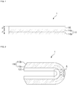
- FIG. 1 is a cross-sectional view of a protection film 10 according to an exemplary embodiment.
- FIG. 2 is a cross-sectional view of the protection film 10 of FIG. 1 in a folded state.
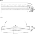
- FIG. 3 is a cross-sectional view illustrating the protection film 10 of FIG. 1 attached to an organic light emitting display device 20.
- the protection film 10 is attached onto a surface of the organic light emitting display device 20. Although not illustrated in the drawings, the protection film 10 may also be attached to cover a portion of the organic light emitting display device 20 which includes not only the surface of the organic light emitting display device 20 but also side edges of the surface.
- the protection film 10 includes a base layer 120 and an adhesive layer 110 disposed on a surface of the base layer 120.
- the base layer 120 may be a layer that substantially protects the organic light emitting display device 20 when the protection film 10 is attached to the organic light emitting display device 20.
- the base layer 120 may include at least one of polyethylene terephthalate (“PET”), polyethylene naphthalate (“PEN”), polycarbonate (“PC”), polymethyl methacrylate (“PMMA”), polystyrene, polyvinylchloride, polyethersulfone (“PES”), polyethylene, polypropylene, TRF film, and combinations of these materials, for example.
- the thickness of the base layer 120 may be about 20 micrometers ( ⁇ m) or more. In an exemplary embodiment, the thickness of the base layer 120 may be about 25 ⁇ m to about 75 ⁇ m, for example. Preferably, the thickness may be about 35 to about 65 micrometers, even more preferred about 45 to about 55 micrometers. By having a thickness within the above range, the base layer 120 may fully protect the surface of the organic light emitting display device 20 without excessively increasing the total thickness of the protection film 10.
- the adhesive layer 110 is disposed on a surface of the base layer 120.
- a surface of the adhesive layer 110 may be an adhesive surface to be attachable or attached to the organic light emitting display device 20.
- the other surface of the adhesive layer 110 may be in contact with the surface of the base layer 120.
- the adhesive layer 110 may directly contact the organic light emitting display device 20.
- the adhesive layer 110 disposed between the base layer 120 and the organic light emitting display device 20 includes the function of attaching the base layer 120 to the organic light emitting display device 20.
- the adhesive layer 110 may be provided using an optically clear adhesive (“OCA”) such as an acrylic-based adhesive, a silicone-based adhesive, a urethane-based adhesive, a rubber-based adhesive or a vinyl ether-based adhesive or may be provided using a pressure sensitive adhesive (“PSA”), for example.
- OCA optically clear adhesive
- PSA pressure sensitive adhesive
- the adhesive layer 110 may include a PSA having a modulus of 10 megapascals (MPa) or less, or of about 5 megapascal or less, or about 1 megapascal or less, each at a temperature of - 20 degrees Celsius (°C) or lower.
- the adhesive layer 110 may include a first region 110a where compressive stress is generated inside the protection film 10 when the protection film 10 is bent and a second region 110b where tensile stress is generated inside the protection film 10 when the protection film 10 is bent.
- compressive stress may be generated in the first region 110a of the adhesive layer 110 which is relatively close to the base layer 120
- tensile stress may be generated in the second region 110b of the adhesive layer 110 which is relatively close to the organic light emitting display device 20, for example.
- a boundary between tensile stress and compressive stress generated in the adhesive layer 110 is illustrated as being a midway point between a surface where the adhesive layer 110 contacts the base layer 120 and a surface where the adhesive layer 110 contacts the organic light emitting display device 20.
- the boundary between the tensile stress and the compressive stress may be provided at a position relatively closer to the surface where the adhesive layer 110 contacts the organic light emitting display device 20 than to the surface where the adhesive layer 110 contacts the base layer 120 or may be provided at a position relatively closer to the surface where the adhesive layer 110 contacts the base layer 120 than to the surface where the adhesive layer 110 contacts the organic light emitting display device 20.
- the thicknesses of the first region 110a and the second region 110b in the adhesive layer 110 may be the same, the thickness of the first region 110a may be relatively greater than the thickness of the second region 110b, or the thickness of the second region 110b may be relatively greater than the thickness of the first region 110a.
- the magnitude of compressive stress in the first region 110a may vary from position to position.
- the compressive stress may be larger as a position is closer to a relatively bent region (e.g., an A region) in the first region 110a.
- the magnitude of tensile stress in the second region 110b may vary from position to position.
- the tensile stress may be larger as a position is closer to the relatively bent region in the second region 110b.
- compressive stress may be generated inside the first region 110a whose length has been increased compared with that before the application of the external force
- tensile stress may be generated inside the second region 110b whose length has been reduced compared with that before the application of the external force.
- the adhesive layer 110 of the protection film 10 has a thickness equal to or smaller than a maximum usable thickness. Thus, buckling may not occur even when the protection film 10 is repeatedly folded and unfolded more than 1000 times.
- the maximum usable thickness of the adhesive layer 110 will be described in detail later.
- the protection film 10 may have a light transmittance of about 90 percent(%) or more and a haze of about 1% or less, specifically, a light transmittance of about 91% to about 95% and a haze of about 0.5% to about 0.8%.
- the protection film 10 may exhibit excellent optical properties by having a light transmittance and a haze within the above ranges.
- the light transmittance may be a value measured according to the conditions of ISO 13468
- the haze may be a value measured according to the conditions of ISO 14782, for example.
- the base layer 120 of the protection film 10 may have a modulus of about 2 gigapascals (GPa) to about 9 GPa, preferably of about 4 gigapascals to about 7 gigapascals, more preferred of about 5 gigapascals to about 6 gigapascals according to the conditions of ASTM D638, for example.
- GPa gigapascals
- ASTM D638 the base layer 120 may exhibit both sufficient durability and excellent flexibility.
- the base layer 120 may have a modulus of about 2 GPa to about 9 GPa, preferably of about 4 gigapascals to about 7 gigapascals, more preferred of about 5 gigapascals to about 6 gigapascals, even under a temperature condition of about - 40 °C to about 80 °C.
- the protection film 10 may be easily deformed permanently.
- the modulus of the base layer 120 is more than about 9 GPa, fissures or cracks may be easily provided in the protection film 10 due to bending or the like.
- the protection film 10 may have excellent optical properties, sufficient durability, and excellent flexibility. Also, even when the protection film 10 is applied to a substrate 210 (including, e.g., a transparent plastic material) of the organic light emitting display device 20, its improved flexibility may prevent breakage or formation of bright dots. Therefore, even when scratches are temporarily generated on the surface of the protection film 10, the surface of the protection film 10 may be restored to its original shape over time due to its elasticity to resist external stimulation or friction.
- the protection film 10 may maintain excellent optical properties and excellent durability for a long time.
- the maximum usable thickness of the adhesive layer 110 may be z1.
- the thickness of the base layer 120 and the thickness of the adhesive layer 110 will be described later, together with their relationship with the modulus of the base layer 120.
- the organic light emitting display device 20 may include the substrate 210, an organic light emitting element layer 220 disposed on the substrate 210, an encapsulation layer 230 disposed on the organic light emitting element layer 220, a touch sensing layer 240 disposed on the encapsulation layer 230, and a cover window 250 disposed on the touch sensing layer 240.
- the substrate 210 may be a flexible display substrate.
- the flexible display substrate is characterized by including a flexible material that may be bent or folded.
- the flexible display substrate may include a plastic film such as a polyimide film or may include sheet glass or a thin metal film, for example.
- the substrate 210 may also be a rigid display substrate.
- the organic light emitting element layer 220 is disposed on the substrate 210.
- a buffer layer may be provided between the substrate 210 and the organic light emitting element layer 220 to flatten an upper surface of the substrate 210 and block the penetration of impurities into the organic light emitting element layer 220.
- the organic light emitting element layer 220 may include a plurality of thin-film transistors ("TFTs”) and a plurality of organic light emitting diodes ("OLEDs").
- TFTs thin-film transistors
- OLEDs organic light emitting diodes
- Each of the OLEDs may be a structure in which an anode, an organic light emitting layer, and a cathode are sequentially stacked.
- Source/drain electrodes of some of the TFTs may be electrically connected to the anodes of the OLEDs.
- the encapsulation layer 230 is provided over the entire surface of the substrate 210 so as to cover the organic light emitting element layer 220.
- the encapsulation layer 230 is provided to protect the OLEDs from external moisture, oxygen, or the like.
- the encapsulation layer 230 may include multiple layers or a single layer including an insulating inorganic material.
- the inorganic material may be a metal oxide or a metal nitride.
- the inorganic material may be silicon oxide (SiO 2 ), silicon nitride (SiNx), silicon oxynitride (SiON), aluminum oxide (Al 2 O 3 ), titanium oxide (TiO 2 ), tantalum oxide (Ta 2 O 5 ), hafnium oxide (HfO 2 ), or zinc oxide (ZrO 2 ), for example.
- the encapsulation layer 230 may form an encapsulation structure in which a thin film including an organic material and a thin film including an inorganic material are further alternately stacked on a thin film including an insulating organic material.
- the organic light emitting display device 20 employing the flexible display substrate 210 and the encapsulation layer 230 made flexible by being provided as a thin film may be bent, folded, or unfolded.
- the touch sensing layer 240 may be disposed on the encapsulation layer 230.
- the touch sensing layer 240 may be an electrostatic capacitive type touch screen panel in an exemplary embodiment. However, the invention is not limited thereto, and in another exemplary embodiment, the touch sensing layer 240 may also be any one of resistive type, electromagnetic type, surface acoustic wave ("SAW") type, and infrared type touch screen panels. Like the flexible display substrate 210, the touch sensing layer 240 uses a flexible material that may be bent or folded. However, the invention is not limited thereto, and in another exemplary embodiment, the touch sensing layer 240 may be omitted.
- the cover window 250 is disposed on the touch sensing layer 240. Although not illustrated, the cover window 250 may be attached to the touch sensing layer 240 using an OCA or optically clear resin ("OCR") disposed between the cover window 250 and the touch sensing layer 240.
- OCA optically clear resin
- the cover window 250 may include glass having a high modulus.
- the modulus of the cover window 250 may be about 50 GPa or more, or about 60 GPa or more, or about 70 GPa or more in an exemplary embodiment.
- the cover window 250 having a high modulus may help prevent buckling from occurring easily even when the adhesive layer 110 of the protection film 10 attached to the cover window 250 becomes thick.
- the cover window 250 may include a window film 251 and a coating layer 252 disposed on a surface of the window film 251 to lower the probability of a damage of the window film 251.
- the window film 251 may include a transparent plastic film.
- the plastic film may include, but is not limited to, polyethylene terephthalate, polymethyl methacrylate, polycarbonate, or polyimide, for example.
- the material of the cover window 250 is not limited to the above-mentioned glass and, in another exemplary embodiment, the material of the cover window 250 may be a flexible material that enables the organic light emitting display device 20 to be bent, folded, and unfolded.
- Light emitted from the organic light emitting element layer 220 may be seen by a user through the cover window 250.
- the protection film 10 may be attached onto the cover window 250 which is the light emitting surface.
- the cover window 250 of the organic light emitting display device 20 described above may be easily damaged by an external impact even when it includes the coating layer 252. Therefore, the protection film 10 as disclosed above or as disclosed in the following embodiments described with respect to Figs. 9 to 10 or combinations thereof is attached onto the cover window 250 so as to prevent the organic light emitting display device 20 from being easily damaged by an external impact.
- FIG. 4 is a cross-sectional view illustrating a process in which the organic light emitting display device 20 to which the protection film 10 of in FIG. 1 has been attached is folded.
- FIG. 5 is a cross-sectional view illustrating a process in which the organic light emitting display device 20 to which the protection film 10 of FIG. 1 or of one of the following embodiments described with respect to Figs. 9 and 10 or combinations thereof has been attached is unfolded.
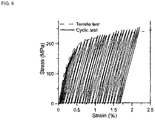
- FIG. 6 is a graph illustrating the amount of tensile stress according to the strain of the adhesive layer 110 in the A region when the processes of FIGS. 4 and 5 are repeated.
- FIG. 7 is a graph illustrating the strain of the adhesive layer 110 according to the thickness of the adhesive layer 110 for each thickness of the base layer 120.
- FIG. 8 is a cross-sectional view illustrating, as a comparative example, a folded protection film 10_1 to which an adhesive layer 110_1 having a thickness exceeding the maximum usable thickness has been applied.
- the organic light emitting display device 20 may be a foldable display device 20, and the protection film 10 according to the exemplary embodiments of Figs. 1 , 9 or 10 may be attached onto the foldable display device 20.
- the organic light emitting display device 20 may be folded and unfolded in the A region.
- the protection film 10 attached onto the organic light emitting display device 20 may also be folded and unfolded in the A region, like the organic light emitting display device 20.
- a direction in which the organic light emitting display device 20 is folded may be a direction in which the light emitting surface faces inward. That is, when the protection film 10 is attached onto the cover window 250 of the organic light emitting display device 20, the organic light emitting display device 20 may be folded such that the radius of curvature becomes greater in the order of the base layer 120, the adhesive layer 110, the cover window 250 and the substrate 210 in the A region.
- the radius of curvature of the base layer 120 may be about 0.5 R or more, or about 0.6 R or more, or about 0.7 R or more, for example. In an exemplary embodiment, the radius of curvature of the base layer 120 may be about 0.5 R to about 1.5 R, for example, or about 0,7 R to about 1.3 R.
- the radius of curvature of the base layer 120 may be the radius of curvature of the adhesive surface where the base layer 120 and the adhesive layer 110 are attached.
- an angle ⁇ defined by a tangent to a side surface of the base layer 120 and an inclined surface of the adhesive layer 110 may be 2 degrees or more, for example.
- the angle ⁇ may be 3 degrees to 25 degrees, preferably from about 8 degrees to about 20 degrees, more preferred from about 12 degrees to about 15 degrees, for example.
- the illustrated graph represents a first experimental example and shows the tensile stress in the adhesive layer 110 and the tensile strain of the adhesive layer 110 in a case where the organic light emitting display device 20 to which the protection film 10 has been attached is repeatedly folded and unfolded as illustrated in FIGS. 4 and 5 .
- the tensile strain is the ratio of the increase in length caused by applied tensile load to the original length.
- tensile stress applied to the adhesive layer 110 may be close to 0 MPa.
- the protection film 10 starts to be folded due to an external force as illustrated in FIG. 4
- the tensile strain may increase, and the tensile stress of the adhesive layer 110 may increase.
- the protection film 10 starts to be unfolded due to an external force as illustrated in FIG. 5
- the tensile strain may increase, and the tensile stress of the adhesive layer 110 may decrease.
- FIG. 5 a solid line graph (cyclic test) of FIG. 6
- the tensile strain is reduced because the protection film 10 returns to its original shape as it is unfolded. At this time, since the shape of the adhesive layer 110 is partially restored, the tensile strain is partially reduced together with the tensile stress. However, in the case of FIG. 5 , the tensile strain of the adhesive layer 110 may not be restored to 0 % because deformation exceeding a restoration critical point has occurred. Although not illustrated in the drawing, when the folding and unfolding of the protection film 10 are repeated, the tensile strain may become close to a maximum tensile strain.
- the adhesive layer 110 may buckle.
- maximum tensile stress per cycle when the process of folding and unfolding the protection film 10 once is referred to as a cycle, maximum tensile stress per cycle may exist.
- the protection film 10 may include the maximum tensile stress per cycle when it is folded to the maximum.
- the maximum tensile stress per cycle may increase sharply until it reaches about 200 MPa, but may increase gradually from 200 MPa or more, for example. That is, the rate of change in the maximum tensile stress per cycle may start to be reduced from around 200 MPa, for example.
- FIG. 6 is an exemplary graph for explaining the change in the tensile strain of the protection film 10 and the tensile stress in the protection film 10 when the process of folding and unfolding the protection film 10 is repeated.
- the tensile strain of the protection film 10 and the tensile stress inside the protection film 10 are not limited to values indicated by this graph in all experimental examples.
- the rate of change in the tensile stress inside the protection film 10 may start to be reduced from around a value other than about 200 MPa, and the tensile strain of the protection film 10 may increase or decrease at a larger rate of change or may increase or decrease at a smaller rate of change, for example.
- FIG. 7 a number of experiments were conducted to identify the usable thickness of the adhesive layer 110 and the maximum compressive strain of the adhesive layer 110 according to the modulus and thickness of the base layer 120 under a high temperature condition of about 65 °C when the base layer 120 had a radius of curvature of 1.5 R.
- the graph of experimental results illustrated in FIG. 7 shows the maximum compressive strain of the adhesive layer 110 after the organic light emitting display device 20 to which the protection film 10 has been attached is folded and unfolded more than 1000 times as illustrated in FIGS. 4 to 6 .
- the compressive strain is a strain according to external compressive stress and may have a sign opposite to that of the tensile strain of FIG. 6 .
- an experimenter attached adhesive layers 110 having thicknesses of about 25 ⁇ m, about 35 ⁇ m, about 50 ⁇ m, about 75 ⁇ m and about 100 ⁇ m to the base layer 120 in order to identify the maximum compressive strain of each adhesive layer 110 and whether each adhesive layer 110 buckled.
- the horizontal axis represents the thickness of the adhesive layer 110
- the vertical axis represents the maximum compressive strain of the adhesive layer 110.
- the maximum compressive strain will be described based on an absolute value.
- a protection film 10_2 according to a second experimental example includes a base layer 120 having a thickness of about 25 ⁇ m and a modulus of about 4.15 GPa. Referring to the second experimental example, as the thickness of the adhesive layer 110 increases, the maximum compressive strain of the adhesive layer 110 increases from about 0.51% at a thickness of 25 ⁇ m of the adhesive layer 110. However, when the thickness of the adhesive layer 110 was about 75 ⁇ m and about 100 ⁇ m, the adhesive layer 110 buckled.
- a protection film 10_3 according to a third experimental example includes a base layer 120 having a thickness of about 35 ⁇ m and a modulus of about 4.15 GPa.
- the maximum compressive strain of the adhesive layer 110 increases from about 0.50% at a thickness of 25 ⁇ m of the adhesive layer 110.
- the maximum compressive strain of the adhesive layer 110 has a smaller value at each thickness of the adhesive layer 110 than in the second experimental example.
- the thickness of the adhesive layer 110 was about 75 ⁇ m and about 100 ⁇ m, the adhesive layer 110 buckled.
- a protection film 10_4 according to a fourth experimental example includes a base layer 120 having a thickness of about 40 ⁇ m and a modulus of about 4.15 GPa.
- the maximum compressive strain of the adhesive layer 110 increases from about 0.49% at a thickness of 25 ⁇ m of the adhesive layer 110.
- the maximum compressive strain of the adhesive layer 110 has a smaller value at each thickness of the adhesive layer 110 than in the third experimental example. When the thickness of the adhesive layer 110 was about 100 ⁇ m, the adhesive layer 110 buckled.
- a protection film 10_5 according to a fifth experimental example includes a base layer 120 having a thickness of about 50 ⁇ m and a modulus of about 4.15 GPa.
- the maximum compressive strain of the adhesive layer 110 decreases from about 0.49% at a thickness of 25 ⁇ m of the adhesive layer 110 and then increases.
- the maximum compressive strain of the adhesive layer 110 has a smaller value at each thickness of the adhesive layer 110 than in the fourth experimental example. In all cases where the thickness of the adhesive layer 110 was about 25 ⁇ m, about 35 ⁇ m, about 50 ⁇ m, about 75 ⁇ m and about 100 ⁇ m, buckling did not occur.
- a protection film 10_6 according to a sixth experimental example includes a base layer 120 having a thickness of about 65 ⁇ m and a modulus of about 4.15 GPa.
- the maximum compressive strain of the adhesive layer 110 decreases from about 0.50% at a thickness of 25 ⁇ m of the adhesive layer 110 and then increases.
- the maximum compressive strain of the adhesive layer 110 does not always have a smaller value at each thickness of the adhesive layer 110 than in the fifth experimental example, but has higher values at some small thicknesses of the adhesive layer 110. In all cases where the thickness of the adhesive layer 110 was about 25 ⁇ m, about 35 ⁇ m, about 50 ⁇ m, about 75 ⁇ m and about 100 ⁇ m, buckling did not occur.
- a protection film 10_7 according to a seventh experimental example includes a base layer 120 having a thickness of about 75 ⁇ m and a modulus of about 4.15 GPa.
- the maximum compressive strain of the adhesive layer 110 decreases from about 0.51% at a thickness of 25 ⁇ m of the adhesive layer 110 and then increases.
- the maximum compressive strain of the adhesive layer 110 does not always have a smaller value at each thickness of the adhesive layer 110 than in the sixth experimental example, but has higher values at some small thicknesses of the adhesive layer 110. In all cases where the thickness of the adhesive layer 110 was about 25 ⁇ m, about 35 ⁇ m, about 50 ⁇ m, about 75 ⁇ m and about 100 ⁇ m, buckling did not occur.
- a protection film 10_8 according to an eighth experimental example includes a base layer 120 having a thickness of about 25 ⁇ m and a modulus of about 6.0 GPa.
- the maximum compressive strain of the adhesive layer 110 increases from about 0.445% at a thickness of 25 ⁇ m of the adhesive layer 110.
- the maximum compressive strain of the adhesive layer 110 has a smaller value at each thickness of the adhesive layer 110 than in the seventh experimental example.
- the thickness of the adhesive layer 110 was about 75 ⁇ m and about 100 ⁇ m, the adhesive layer 110 buckled.
- a protection film 10_9 according to a ninth experimental example includes a base layer 120 having a thickness of about 35 ⁇ m and a modulus of about 6.0 GPa.
- the maximum compressive strain of the adhesive layer 110 increases from about 0.44% at a thickness of 25 ⁇ m of the adhesive layer 110.
- the maximum compressive strain of the adhesive layer 110 has a smaller value at each thickness of the adhesive layer 110 than in the eighth experimental example.
- the thickness of the adhesive layer 110 was about 75 ⁇ m and about 100 ⁇ m, the adhesive layer 110 buckled.
- a protection film 10_10 according to a tenth experimental example includes a base layer 120 having a thickness of about 40 ⁇ m and a modulus of about 6.0 GPa.
- the maximum compressive strain of the adhesive layer 110 decreases from about 0.43% at a thickness of 25 ⁇ m of the adhesive layer 110 and then increases.
- the maximum compressive strain of the adhesive layer 110 has a smaller value at each thickness of the adhesive layer 110 than in the ninth experimental example. In all cases where the thickness of the adhesive layer 110 was about 25 ⁇ m, about 35 ⁇ m, about 50 ⁇ m, about 75 ⁇ m and about 100 ⁇ m, buckling did not occur.
- a protection film 10_11 according to an eleventh experimental example includes a base layer 120 having a thickness of about 50 ⁇ m and a modulus of about 6.0 GPa.
- the maximum compressive strain of the adhesive layer 110 decreases from about 0.43% at a thickness of 25 ⁇ m of the adhesive layer 110 and then increases.
- the maximum compressive strain of the adhesive layer 110 has a smaller value at each thickness of the adhesive layer 110 than in the tenth experimental example. In all cases where the thickness of the adhesive layer 110 was about 25 ⁇ m, about 35 ⁇ m, about 50 ⁇ m, about 75 ⁇ m and about 100 ⁇ m, buckling did not occur.
- a protection film 10_12 according to a twelfth experimental example includes a base layer 120 having a thickness of about 65 ⁇ m and a modulus of about 6.0 GPa.
- the maximum compressive strain of the adhesive layer 110 decreases from about 0.44% at a thickness of 25 ⁇ m of the adhesive layer 110 and then increases.
- the maximum compressive strain of the adhesive layer 110 does not always have a smaller value at each thickness of the adhesive layer 110 than in the eleventh experimental example, but has higher values at some small thicknesses of the adhesive layer 110. In all cases where the thickness of the adhesive layer 110 was about 25 ⁇ m, about 35 ⁇ m, about 50 ⁇ m, about 75 ⁇ m and about 100 ⁇ m, buckling did not occur.
- a protection film 10_13 according to a thirteenth experimental example includes a base layer 120 having a thickness of about 25 ⁇ m and a modulus of about 9.0 GPa.
- the maximum compressive strain of the adhesive layer 110 increases from about 0.38% at a thickness of 25 ⁇ m of the adhesive layer 110.
- the maximum compressive strain of the adhesive layer 110 has a smaller value at each thickness of the adhesive layer 110 than in the twelfth experimental example.
- the thickness of the adhesive layer 110 was about 75 ⁇ m and about 100 ⁇ m, the adhesive layer 110 buckled.
- a protection film 10_14 according to a fourteenth experimental example includes a base layer 120 having a thickness of about 35 ⁇ m and a modulus of about 9.0 GPa.
- the maximum compressive strain of the adhesive layer 110 increases from about 0.37% at a thickness of 25 ⁇ m of the adhesive layer 110.
- the maximum compressive strain of the adhesive layer 110 has a smaller value at each thickness of the adhesive layer 110 than in the thirteenth experimental example.
- the thickness of the adhesive layer 110 was about 100 ⁇ m, the adhesive layer 110 buckled.
- a protection film 10_15 according to a fifteenth experimental example includes a base layer 120 having a thickness of about 40 ⁇ m and a modulus of about 9.0 GPa.
- the maximum compressive strain of the adhesive layer 110 decreases from about 0.36% at a thickness of 25 ⁇ m of the adhesive layer 110 and then increases.
- the maximum compressive strain of the adhesive layer 110 has a smaller value at each thickness of the adhesive layer 110 than in the fourteenth experimental example. In all cases where the thickness of the adhesive layer 110 was about 25 ⁇ m, about 35 ⁇ m, about 50 ⁇ m, about 75 ⁇ m and about 100 ⁇ m, buckling did not occur.
- the maximum usable thickness of the adhesive layer 110 could be about 77 ⁇ m.
- the maximum usable thickness of the adhesive layer 110 could be about 84 ⁇ m.
- the maximum usable thickness of the adhesive layer 110 could be about 94 ⁇ m.
- the maximum usable thickness of the adhesive layer 110 could be about 87 ⁇ m.
- the maximum usable thickness of the adhesive layer 110 could be about 96 ⁇ m.
- the maximum usable thickness of the adhesive layer 110 could be about 108 ⁇ m.
- the maximum usable thickness of the adhesive layer 110 could be about 104 ⁇ m.
- the maximum usable thickness of the adhesive layer 110 could be about 116 ⁇ m.
- the maximum usable thickness of the adhesive layer 110 could be about 131 ⁇ m.
- the maximum usable thickness of the adhesive layer 110 could be about 124 ⁇ m.
- the maximum usable thickness of the adhesive layer 110 could be about 139 ⁇ m.
- the maximum usable thickness of the adhesive layer 110 could be about 158 ⁇ m.
- the maximum usable thickness of the adhesive layer 110 could be about 135 ⁇ m.
- the maximum usable thickness of the adhesive layer 110 could be about 151 ⁇ m.
- the maximum usable thickness of the adhesive layer 110 could be about 173 ⁇ m.
- Equation 3 the maximum usable thickness of the adhesive layer 110 according to the modulus of the base layer 120 and the thickness of the base layer 120 substantially satisfied Equation 3 below.
- z 5.1 x + 57.4 ⁇ ln y ⁇ 14.7 x + 140.5
- x is the modulus value of the base layer 120 measured in GPa
- y is the thickness value of the base layer 120 measured in ⁇ m
- z is the maximum usable thickness of the adhesive layer 110 measured in ⁇ m.
- z 1 5.1 x 1 + 57.4 ⁇ ln y 1 ⁇ 14.7 x 1 + 140.5
- z1 satisfying Equation 4 corresponds to the maximum usable thickness of the adhesive layer 110. Therefore, when the adhesive layer 110 of the protection film 10 has a thickness of z1 or less, buckling may not occur even when the protection film 10 is repeatedly folded and unfolded more than 1000 times, for example.
- the protection film 10_1 may include the adhesive layer 110_1 having a thickness exceeding z1 that satisfies Equation 4.
- buckling of the adhesive layer 110_1 may occur in a folding and unfolding region.
- the buckling may occur mostly near the boundary of a bent portion.
- the buckling may occur not only near the boundary on one side of the bent portion as illustrated in the drawing, but also near the boundary on the other side of the bent portion.
- the buckling does not occur when the protection film 10_1 is used in a flexible display device or a rigid display device instead of the foldable organic light emitting display device 20, it is possible to prevent the organic light emitting display device 20 from being damaged.
- Table 2 The values shown in Table 2 are approximate values, and some minor errors may exist. [Table 2] Comparative example Sixteenth experimental example Seventeenth experimental example Eighteenth experimental example Nineteenth experimental example DuPont impact test Bright dots at 2 cm Bright dots at 5 cm Bright dots at 7 cm Bright dots at 3 cm Bright dots at 4 cm Pen drop test Broken at 1 cm Broken at 13 cm Broken at 16 cm Broken at 16 cm Broken at 8 cm
- the comparative example was conducted without attaching the protection film 10 to the organic light emitting display device 20.
- a protection film 10 including a base layer 120 having a thickness of about 40 ⁇ m and a modulus of about 4.15 GPa and an adhesive layer 110 having a thickness of about 50 ⁇ m were attached.
- a protection film 10 including a base layer 120 having a thickness of about 40 ⁇ m and a modulus of about 4.15 GPa and an adhesive layer 110 having a thickness of about 100 ⁇ m were attached.
- a protection film 10 including a base layer 120 having a thickness of about 50 ⁇ m and a modulus of about 4.15 GPa and an adhesive layer 110 having a thickness of about 50 ⁇ m were attached.
- a protection film 10 including a base layer 120 having a thickness of about 25 ⁇ m and a modulus of about 1.5 GPa and an adhesive layer 110 having a thickness of about 50 ⁇ m were attached.
- the height that caused bright dots to be provided increased as the thickness of the adhesive layer 110 increased.
- the cover window 250 of the organic light emitting display device 20 was very vulnerable when the protection film 10 was not attached, but the height that caused the cover window 250 to be broken increased sharply as the modulus of the base layer 120 and the thickness of the protection film 10 increased.
- the protection film 10 includes an adhesive layer 110 having a maximum thickness that does not cause buckling according to the modulus and thickness of the base layer 120.
- FIG. 9 is a cross-sectional view of a protection film 11 according to an exemplary embodiment.
- the protection film 11 is different from the protection film 10 of FIG. 1 in that a functional layer 130 is further attached onto a base layer 120.
- the protection film 11 may include an adhesive layer 110, the base layer 120, and the functional layer 130.
- the base layer 120 may be disposed on the adhesive layer 110, and the functional layer 130 may be disposed on the base layer 120.
- the functional layer 130 may include any one or more of an anti-fingerprint coating layer, an anti-fouling coating layer, an anti-reflection coating layer, an anti-glare coating layer, a hard-coating layer, and a self-restoring layer.
- the illustrated exemplary embodiment to be described below merely explains a structure in which the functional layer 130 includes a hard-coating layer 131, an anti-fingerprint coating layer 132 and a self-restoring layer 133 and is not limited to this structure.
- the hard-coating layer 131 may be disposed on the base layer 120.
- the hard-coating layer 131 disposed on the base layer 120 may reduce the distortion or lifting phenomenon of the protection film 11 under severe conditions such as high temperature or high temperature and high humidity, thereby improving reliability.
- the hard-coating layer 131 may include an organic layer and an organic-inorganic composite layer.
- the organic layer may include an acrylate-based compound.
- the organic layer may include urethane acrylate, for example.
- the organic layer may be disposed between the base layer 120 and the organic-inorganic composite layer to serve as a stress buffer layer.
- the organic layer may have a thickness of about 20 ⁇ m or less, for example.
- An organic material in the organic-inorganic composite layer may include at least one or a combination of an acrylate-based compound, a polyurethane-based compound, and an epoxy-based compound.
- first and second organic-inorganic composite layers may include urethane acrylate, for example.
- an inorganic material in the organic-inorganic composite layer may be at least any one of silicon oxide (SiO 2 ), zirconium oxide (ZrO 2 ), aluminum oxide (Al 2 O 3 ), tantalum oxide (Ta 2 O 5 ), niobium oxide (Nb 2 O 5 , NbO 2 ), and glass bead, for example.
- the inorganic material may be provided in the form of a single kind of inorganic oxide listed or a combination of these materials.
- the inorganic material may be provided in various forms to form the organic-inorganic composite layer.
- silicon oxide may be provided in the form of SiO 2 particles, a SiO 2 sol in which SiO 2 particles are dispersed in a colloidal state, or SiO 2 having a hollow shape, for example.
- an acrylate compound i.e., an organic material
- inorganic particles may be mixed in a weight ratio of 5: 5 to 8: 2, for example.
- the organic-inorganic composite layer may form the hard-coating layer 131 that has improved surface hardness and is not easily broken due to its ability to absorb external shock.
- the anti-fingerprint coating layer 132 may be disposed on the hard-coating layer 131.
- the anti-fingerprint coating layer 132 is provided by providing a coating material including perfluoropolyether using a spray coating method and thermally curing the coating material at about 60 °C for about 60 minutes, for example.
- the provided anti-fingerprint coating layer 132 may have a thickness of about 50 ⁇ m, for example.
- the anti-fingerprint coating layer 132 may be provided using not only the above-described method, but also using various methods.
- the self-restoring layer 133 may be disposed on the anti-fingerprint coating layer 132.
- the self-restoring layer 133 is provided using a self-restoring composition including aromatic urethane acrylate resins.
- the urethane acrylate resins may be included in a ladder structure that may be supported by an aromatic group, a heteroaromatic group, or both.
- the aromatic urethane acrylate resins may be urethane acrylate resins having 2 to 5 functional groups on average, may be provided by reacting a polymerizable composition including acrylate, which includes a hydroxyl group, and an isocyanate compound, and at least one of the acrylate including the hydroxyl group and the isocyanate compound may include an aromatic group, a heteroaromatic group, or both.
- the thickness of the self-restoring layer 133 may be about 15 ⁇ m to about 40 ⁇ m, for example.
- the self-restoring layer 133 may exhibit sufficient bending and self-restoring properties without excessively increasing the total thickness of the protection film 11.
- the self-restoring layer 133 may have uniform performance over a long period of time.
- the maximum usable thickness of the adhesive layer 110 may be applied according to Equation 3 regarding the relationship between the base layer 120 and the adhesive layer 110 when the radius of curvature of the base layer 120 is about 0.5 R or more, the thickness of the base layer 120 is about 25 ⁇ m to about 75 ⁇ m, the modulus of the base layer 120 is about 2 GPa to about 9 GPa, and the temperature is about -40 °C to about 65 °C, for example.
- the maximum usable thickness of the adhesive layer 110 of the protection film 11 according to the illustrated exemplary embodiment may satisfy Equation 5 below.
- y2 is a value obtained by adding not only the thickness of the base layer 120 but also the thickness of the functional layer 130. That is, y2 may be the total thickness of all layers stacked on the adhesive layer 110.
- y1 since all layers stacked on the adhesive layer 110 include only the base layer 120 in FIG. 1 , y1 may be the thickness of the base layer 120, for example.
- y2 since all layers stacked on the adhesive layer 110 include the base layer 120 and the functional layer 130, y2 may be the sum of the thickness of the base layer 120 and the thickness of the functional layer 130.
- a damage to the organic light emitting display device 20 due to an external impact may be reduced when the protection film 11 including the adhesive layer 110 of the maximum usable thickness is attached to the organic light emitting display device 20.
- FIG. 10 is a cross-sectional view of a protection film 12 according to an exemplary embodiment.
- the protection film 12 according to the illustrated exemplary embodiment is different from the protection film 11 of FIG. 9 in that it further includes a primer layer 141 disposed between a base layer 120 and a functional layer 130.
- the primer layer 141 may be an adhesion-assisting layer for enhancing the adhesion between the base layer 120 and a hard-coating layer 131.
- the protection film 12 of the illustrated exemplary embodiment may further include the primer layer 141 between the functional layer 130 and the base layer 120.
- the primer layer 141 may be disposed between the base layer 120 and the hard-coating layer 131.
- the primer layer 141 may include a silane coupling agent and isocyanate, for example.
- the primer layer 141 may have a thickness of 10 nanometers (nm) to 30 nm, for example.
- the primer layer 141 When the primer layer 141 is provided thinner than 10 nm, its function as an adhesion-assisting layer may deteriorate, thus weakening the adhesion to the functional layer 130.
- the primer layer 141 when the primer layer 141 is provided thicker than 30 nm, a haze phenomenon may occur, thus degrading optical characteristics of the primer layer 141.
- the maximum usable thickness of an adhesive layer 110 may be applied according to Equation 3 regarding the relationship between the base layer 120 and the adhesive layer 110 when the radius of curvature of the base layer 120 is about 0.5 R or more, the thickness of the base layer 120 is about 25 ⁇ m to about 75 ⁇ m, the modulus of the base layer 120 is about 2 GPa to about 9 GPa, and the temperature is about -40 °C to about 65 °C, for example.
- the maximum usable thickness of the adhesive layer 110 of the protection film 12 according to the illustrated exemplary embodiment may satisfy Equation 6 below.
- z 3 5.1 x 3 + 57.4 ⁇ ln y 3 ⁇ 14.7 x 3 + 140.5 , where x3 is the modulus of the base layer 120. Since y3 is the total thickness of all layers stacked on the adhesive layer 110, it may be, for example, the sum of the thickness of the base layer 120, the thickness of the primer layer 141, and the thickness of the functional layer 130.
- a damage to the organic light emitting display device 20 due to an external impact may be reduced when the protection film 12 including the adhesive layer 110 of the maximum usable thickness is attached to the organic light emitting display device 20.
- a protective film may have excellent durability for a long period of time and protect an electronic device from the outside.
Landscapes
- Engineering & Computer Science (AREA)
- Theoretical Computer Science (AREA)
- Physics & Mathematics (AREA)
- General Physics & Mathematics (AREA)
- Computer Hardware Design (AREA)
- Human Computer Interaction (AREA)
- General Engineering & Computer Science (AREA)
- Mechanical Engineering (AREA)
- Chemical & Material Sciences (AREA)
- Organic Chemistry (AREA)
- Optics & Photonics (AREA)
- Electroluminescent Light Sources (AREA)
- Laminated Bodies (AREA)
- Adhesive Tapes (AREA)
Priority Applications (1)
| Application Number | Priority Date | Filing Date | Title |
|---|---|---|---|
| EP23213968.3A EP4307869A3 (fr) | 2018-09-19 | 2019-09-06 | Film de protection et dispositif électronique le comprenant |
Applications Claiming Priority (1)
| Application Number | Priority Date | Filing Date | Title |
|---|---|---|---|
| KR1020180112073A KR102465207B1 (ko) | 2018-09-19 | 2018-09-19 | 보호 필름 및 그것을 포함하는 전자 기기 |
Related Child Applications (1)
| Application Number | Title | Priority Date | Filing Date |
|---|---|---|---|
| EP23213968.3A Division EP4307869A3 (fr) | 2018-09-19 | 2019-09-06 | Film de protection et dispositif électronique le comprenant |
Publications (2)
| Publication Number | Publication Date |
|---|---|
| EP3633004A1 true EP3633004A1 (fr) | 2020-04-08 |
| EP3633004B1 EP3633004B1 (fr) | 2023-12-06 |
Family
ID=67875297
Family Applications (2)
| Application Number | Title | Priority Date | Filing Date |
|---|---|---|---|
| EP23213968.3A Pending EP4307869A3 (fr) | 2018-09-19 | 2019-09-06 | Film de protection et dispositif électronique le comprenant |
| EP19195826.3A Active EP3633004B1 (fr) | 2018-09-19 | 2019-09-06 | Film de protection et dispositif électronique le comprenant |
Family Applications Before (1)
| Application Number | Title | Priority Date | Filing Date |
|---|---|---|---|
| EP23213968.3A Pending EP4307869A3 (fr) | 2018-09-19 | 2019-09-06 | Film de protection et dispositif électronique le comprenant |
Country Status (4)
| Country | Link |
|---|---|
| US (4) | US10665816B2 (fr) |
| EP (2) | EP4307869A3 (fr) |
| KR (2) | KR102465207B1 (fr) |
| CN (1) | CN110927834A (fr) |
Cited By (7)
| Publication number | Priority date | Publication date | Assignee | Title |
|---|---|---|---|---|
| US10985344B2 (en) | 2017-10-27 | 2021-04-20 | Applied Materials, Inc. | Flexible cover lens films |
| CN113823220A (zh) * | 2020-06-18 | 2021-12-21 | 三星显示有限公司 | 包括窗的显示装置 |
| US11579339B2 (en) | 2018-05-10 | 2023-02-14 | Applied Materials, Inc. | Replaceable cover lens for flexible display |
| US11789300B2 (en) | 2019-06-26 | 2023-10-17 | Applied Materials, Inc. | Flexible multi-layered cover lens stacks for foldable displays |
| US20240160248A1 (en) * | 2022-10-24 | 2024-05-16 | Samsung Display Co., Ltd. | Display device |
| US11988810B2 (en) | 2018-08-14 | 2024-05-21 | Applied Materials, Inc. | Multi-layer wet-dry hardcoats for flexible cover lens |
| US12164340B2 (en) | 2021-07-29 | 2024-12-10 | Samsung Display Co., Ltd. | Display device |
Families Citing this family (27)
| Publication number | Priority date | Publication date | Assignee | Title |
|---|---|---|---|---|
| KR102304521B1 (ko) * | 2019-09-26 | 2021-09-24 | 리얼룩앤컴퍼니 주식회사 | 초음파 지문인식이 가능한 액정보호필름 |
| CN111524823A (zh) * | 2020-04-10 | 2020-08-11 | 上海华虹宏力半导体制造有限公司 | 设备的检测方法和测试晶圆 |
| KR102383997B1 (ko) | 2020-04-24 | 2022-04-08 | 주식회사 삼양사 | 히드록시 말단 폴리실록산 혼합물을 이용한 폴리실록산-폴리카보네이트 공중합체 및 그 제조방법 |
| CN113707007A (zh) * | 2020-05-21 | 2021-11-26 | 华为技术有限公司 | 一种显示面板和显示装置 |
| KR102764540B1 (ko) | 2020-07-09 | 2025-02-07 | 삼성디스플레이 주식회사 | 커버 윈도우 보호 필름 및 이를 포함하는 표시 장치 |
| CN111816077B (zh) * | 2020-07-13 | 2022-04-26 | 武汉华星光电半导体显示技术有限公司 | 可折叠显示模组 |
| CN111944439A (zh) * | 2020-08-21 | 2020-11-17 | 四川羽玺科技有限公司 | 一种超爽滑保护膜及其制备方法和应用 |
| KR102929664B1 (ko) * | 2020-08-24 | 2026-02-24 | 삼성디스플레이 주식회사 | 폴더블 윈도우 및 이를 포함하는 표시 장치 |
| WO2022108362A1 (fr) * | 2020-11-18 | 2022-05-27 | 삼성전자 주식회사 | Appareil électronique comprenant un écran souple |
| EP4258249A4 (fr) * | 2021-01-18 | 2024-06-12 | Huawei Technologies Co., Ltd. | Dispositif d'affichage pliable et appareil électronique |
| KR20220105255A (ko) | 2021-01-19 | 2022-07-27 | 삼성디스플레이 주식회사 | 지문방지 코팅용 화합물, 이를 포함하는 디스플레이 보호층 및 전자 장치 |
| KR20220106887A (ko) * | 2021-01-22 | 2022-08-01 | 삼성디스플레이 주식회사 | 표시 장치 |
| CN112908180B (zh) * | 2021-02-07 | 2022-09-09 | 武汉华星光电半导体显示技术有限公司 | 柔性显示模组 |
| KR102837091B1 (ko) * | 2021-03-29 | 2025-07-24 | 삼성디스플레이 주식회사 | 표시 장치 |
| KR102723718B1 (ko) * | 2021-03-31 | 2024-10-31 | 후지필름 가부시키가이샤 | 보호층 및 폴더블 디바이스 |
| CN115440131B (zh) * | 2021-06-01 | 2025-04-15 | 群创光电股份有限公司 | 可卷曲显示装置 |
| CN113782559B (zh) * | 2021-09-14 | 2023-11-07 | 业成科技(成都)有限公司 | 导电模组及显示装置 |
| WO2023059098A1 (fr) * | 2021-10-06 | 2023-04-13 | 삼성전자 주식회사 | Appareil électronique comprenant un élément de protection d'écran d'affichage |
| CN116204076A (zh) * | 2021-11-30 | 2023-06-02 | 宸鸿科技(厦门)有限公司 | 触控显示模块 |
| TWI886452B (zh) * | 2021-12-10 | 2025-06-11 | 大陸商宸鴻科技(廈門)有限公司 | 觸控顯示模組 |
| TWI796044B (zh) * | 2021-12-10 | 2023-03-11 | 大陸商宸鴻科技(廈門)有限公司 | 觸控顯示模組 |
| KR102902674B1 (ko) * | 2021-12-30 | 2025-12-19 | 엘지디스플레이 주식회사 | 표시장치 |
| KR20230137038A (ko) * | 2022-03-21 | 2023-10-04 | 삼성전자주식회사 | 플렉서블 디스플레이를 포함하는 전자 장치 |
| KR20240038845A (ko) | 2022-09-16 | 2024-03-26 | 삼성디스플레이 주식회사 | 보호필름 모듈 및 이를 이용한 표시 장치 제조방법 |
| KR20240045431A (ko) | 2022-09-29 | 2024-04-08 | 삼성디스플레이 주식회사 | 보호필름 모듈 및 이의 제조방법 |
| KR20240059697A (ko) | 2022-10-25 | 2024-05-08 | 삼성디스플레이 주식회사 | 윈도우 및 이를 포함하는 표시장치 |
| WO2025155134A1 (fr) * | 2024-01-17 | 2025-07-24 | 삼성전자 주식회사 | Dispositif électronique comprenant un ensemble fenêtre et procédé de fabrication d'ensemble fenêtre |
Citations (6)
| Publication number | Priority date | Publication date | Assignee | Title |
|---|---|---|---|---|
| US20120171444A1 (en) * | 2009-07-15 | 2012-07-05 | Nitto Denko Corporation | Transparent film and surface-protection film using said film |
| US20150185782A1 (en) | 2013-12-30 | 2015-07-02 | Samsung Electronics Co., Ltd. | Flexible display device, foldable electronic device including the same, and method of manufacturing flexible display device |
| EP3136459A1 (fr) * | 2015-08-31 | 2017-03-01 | LG Display Co., Ltd. | Dispositif à affichage électroluminescent organique flexible |
| US20180112049A1 (en) | 2016-10-21 | 2018-04-26 | Samsung Electronics Co., Ltd. | Stacked transparent film and window for display device and display device |
| US20180258332A1 (en) | 2015-11-12 | 2018-09-13 | Dongwoo Fine-Chem Co., Ltd. | Optical laminate and image display device including the same |
| KR20180112073A (ko) | 2016-06-29 | 2018-10-11 | 애플 인크. | 전자 디스플레이의 가변 프레임 듀레이션 제어를 위한 시스템 및 방법 |
Family Cites Families (15)
| Publication number | Priority date | Publication date | Assignee | Title |
|---|---|---|---|---|
| JP5547132B2 (ja) * | 2011-06-24 | 2014-07-09 | 株式会社東芝 | 半導体装置、その製造方法及び製造装置 |
| KR101539133B1 (ko) * | 2012-07-10 | 2015-07-23 | (주)엘지하우시스 | 반도체 웨이퍼 표면보호 점착필름 및 그의 제조방법 |
| KR20150085352A (ko) * | 2014-01-15 | 2015-07-23 | 삼성디스플레이 주식회사 | 표시 패널의 하부 보호필름 및 이를 포함하는 표시 장치 |
| KR102347532B1 (ko) | 2014-01-23 | 2022-01-05 | 삼성디스플레이 주식회사 | 접을 수 있는 플렉서블 표시 장치 및 이의 제조 방법 |
| JP6528259B2 (ja) | 2014-08-19 | 2019-06-12 | リンテック株式会社 | 表面保護フィルム |
| KR101905245B1 (ko) | 2015-07-31 | 2018-10-05 | 삼성에스디아이 주식회사 | 윈도우 필름 및 이를 포함하는 플렉시블 디스플레이 장치 |
| TWI746465B (zh) | 2015-10-13 | 2021-11-21 | 美商康寧公司 | 可彎式電子裝置模組、物品及其製造方法 |
| KR102494986B1 (ko) * | 2016-01-11 | 2023-02-03 | 삼성디스플레이 주식회사 | 폴더블 표시장치 |
| KR102027570B1 (ko) | 2016-02-25 | 2019-10-01 | 삼성에스디아이 주식회사 | 플렉시블 디스플레이 장치 |
| EP3429970B1 (fr) | 2016-03-17 | 2022-11-23 | Corning Incorporated | Modules souples de dispositif électronique, articles et procédés de liaison destinés à leur fabrication |
| KR102038116B1 (ko) | 2016-03-21 | 2019-12-02 | 주식회사 엘지화학 | 플렉서블 디스플레이용 보호 필름 |
| KR102449220B1 (ko) | 2016-03-21 | 2022-09-30 | 삼성디스플레이 주식회사 | 디스플레이 장치 |
| KR101976902B1 (ko) * | 2016-09-27 | 2019-05-09 | 삼성에스디아이 주식회사 | 윈도우 필름용 보호 필름, 이를 포함하는 광학 부재 및 이를 포함하는 디스플레이 장치 |
| KR102559841B1 (ko) * | 2016-08-18 | 2023-07-27 | 삼성디스플레이 주식회사 | 플렉서블 디스플레이 장치 및 그 제조방법 |
| US10401663B2 (en) * | 2017-03-31 | 2019-09-03 | Panasonic Liquid Crystal Display Co., Ltd. | Curved liquid crystal display and method of manufacturing the same |
-
2018
- 2018-09-19 KR KR1020180112073A patent/KR102465207B1/ko active Active
-
2019
- 2019-04-26 US US16/396,421 patent/US10665816B2/en active Active
- 2019-08-28 CN CN201910801674.4A patent/CN110927834A/zh active Pending
- 2019-09-06 EP EP23213968.3A patent/EP4307869A3/fr active Pending
- 2019-09-06 EP EP19195826.3A patent/EP3633004B1/fr active Active
-
2020
- 2020-04-08 US US16/843,458 patent/US11974452B2/en active Active
-
2021
- 2021-06-25 US US17/357,990 patent/US11812635B2/en active Active
-
2022
- 2022-11-04 KR KR1020220145897A patent/KR102610808B1/ko active Active
-
2023
- 2023-10-10 US US18/378,582 patent/US12484420B2/en active Active
Patent Citations (6)
| Publication number | Priority date | Publication date | Assignee | Title |
|---|---|---|---|---|
| US20120171444A1 (en) * | 2009-07-15 | 2012-07-05 | Nitto Denko Corporation | Transparent film and surface-protection film using said film |
| US20150185782A1 (en) | 2013-12-30 | 2015-07-02 | Samsung Electronics Co., Ltd. | Flexible display device, foldable electronic device including the same, and method of manufacturing flexible display device |
| EP3136459A1 (fr) * | 2015-08-31 | 2017-03-01 | LG Display Co., Ltd. | Dispositif à affichage électroluminescent organique flexible |
| US20180258332A1 (en) | 2015-11-12 | 2018-09-13 | Dongwoo Fine-Chem Co., Ltd. | Optical laminate and image display device including the same |
| KR20180112073A (ko) | 2016-06-29 | 2018-10-11 | 애플 인크. | 전자 디스플레이의 가변 프레임 듀레이션 제어를 위한 시스템 및 방법 |
| US20180112049A1 (en) | 2016-10-21 | 2018-04-26 | Samsung Electronics Co., Ltd. | Stacked transparent film and window for display device and display device |
Cited By (16)
| Publication number | Priority date | Publication date | Assignee | Title |
|---|---|---|---|---|
| US12108622B2 (en) | 2017-10-27 | 2024-10-01 | Applied Materials, Inc. | Flexible cover lens films |
| US10985344B2 (en) | 2017-10-27 | 2021-04-20 | Applied Materials, Inc. | Flexible cover lens films |
| US11758757B2 (en) | 2017-10-27 | 2023-09-12 | Applied Materials, Inc. | Flexible cover lens films |
| US11579339B2 (en) | 2018-05-10 | 2023-02-14 | Applied Materials, Inc. | Replaceable cover lens for flexible display |
| US11988810B2 (en) | 2018-08-14 | 2024-05-21 | Applied Materials, Inc. | Multi-layer wet-dry hardcoats for flexible cover lens |
| US11940683B2 (en) | 2019-06-26 | 2024-03-26 | Applied Materials, Inc. | Flexible multi-layered cover lens stacks for foldable displays |
| US11940682B2 (en) | 2019-06-26 | 2024-03-26 | Applied Materials, Inc. | Flexible multi-layered cover lens stacks for foldable displays |
| US11934056B2 (en) | 2019-06-26 | 2024-03-19 | Applied Materials, Inc. | Flexible multi-layered cover lens stacks for foldable displays |
| US11789300B2 (en) | 2019-06-26 | 2023-10-17 | Applied Materials, Inc. | Flexible multi-layered cover lens stacks for foldable displays |
| US12292634B2 (en) | 2019-06-26 | 2025-05-06 | Applied Materials, Inc. | Flexible multi-layered cover lens stacks for foldable displays |
| US12292635B2 (en) | 2019-06-26 | 2025-05-06 | Applied Materials, Inc. | Flexible multi-layered cover lens stacks for foldable displays |
| CN113823220A (zh) * | 2020-06-18 | 2021-12-21 | 三星显示有限公司 | 包括窗的显示装置 |
| US11829204B2 (en) | 2020-06-18 | 2023-11-28 | Samsung Display Co., Ltd. | Window and display device including the same |
| EP3926439A3 (fr) * | 2020-06-18 | 2022-04-27 | Samsung Display Co., Ltd. | Fenêtre et dispositif d'affichage la comprenant |
| US12164340B2 (en) | 2021-07-29 | 2024-12-10 | Samsung Display Co., Ltd. | Display device |
| US20240160248A1 (en) * | 2022-10-24 | 2024-05-16 | Samsung Display Co., Ltd. | Display device |
Also Published As
| Publication number | Publication date |
|---|---|
| US20200091458A1 (en) | 2020-03-19 |
| US11974452B2 (en) | 2024-04-30 |
| US20240040825A1 (en) | 2024-02-01 |
| EP4307869A3 (fr) | 2024-05-22 |
| US10665816B2 (en) | 2020-05-26 |
| KR102610808B1 (ko) | 2023-12-06 |
| CN110927834A (zh) | 2020-03-27 |
| US12484420B2 (en) | 2025-11-25 |
| EP3633004B1 (fr) | 2023-12-06 |
| US20210320279A1 (en) | 2021-10-14 |
| US20200235340A1 (en) | 2020-07-23 |
| KR102465207B1 (ko) | 2022-11-09 |
| US11812635B2 (en) | 2023-11-07 |
| EP4307869A2 (fr) | 2024-01-17 |
| KR20200033366A (ko) | 2020-03-30 |
| KR20220151593A (ko) | 2022-11-15 |
Similar Documents
| Publication | Publication Date | Title |
|---|---|---|
| US12484420B2 (en) | Protection film including base layer over adhesive layer | |
| US11235554B2 (en) | Window member and display device including the same | |
| EP3173856A1 (fr) | Vitrage, dispositif d'affichage le comprenant et procédé de fabrication du vitrage | |
| US11930693B2 (en) | Flexible display device and method for manufacturing the same | |
| US11579339B2 (en) | Replaceable cover lens for flexible display | |
| EP3582063B1 (fr) | Fenêtre et dispositif d'affichage la comprenant | |
| US20240196554A1 (en) | Cover plate and display device | |
| EP3299162B1 (fr) | Fenêtre pour dispositif d'affichage et dispositif d'affichage | |
| US20180346751A1 (en) | Highly functional af hard coating film | |
| US10401906B2 (en) | Cover window for display device and display device including the same | |
| CN111469513A (zh) | 用于显示屏的保护膜及其制备方法和电子设备 | |
| US20230184998A1 (en) | Window and electronic device including the same | |
| US20130309433A1 (en) | Screen protective film structure | |
| CN116744716A (zh) | 显示装置 | |
| CN115938221A (zh) | 显示装置 | |
| KR20220106887A (ko) | 표시 장치 | |
| US20220389290A1 (en) | Window and display device including the same | |
| CN220550134U (zh) | 保护膜、柔性显示屏和电子设备 | |
| US20240318050A1 (en) | Adhesive composition and display apparatus including the same | |
| CN119511421A (zh) | 显示装置及其制造方法 |
Legal Events
| Date | Code | Title | Description |
|---|---|---|---|
| PUAI | Public reference made under article 153(3) epc to a published international application that has entered the european phase |
Free format text: ORIGINAL CODE: 0009012 |
|
| STAA | Information on the status of an ep patent application or granted ep patent |
Free format text: STATUS: THE APPLICATION HAS BEEN PUBLISHED |
|
| AK | Designated contracting states |
Kind code of ref document: A1 Designated state(s): AL AT BE BG CH CY CZ DE DK EE ES FI FR GB GR HR HU IE IS IT LI LT LU LV MC MK MT NL NO PL PT RO RS SE SI SK SM TR |
|
| AX | Request for extension of the european patent |
Extension state: BA ME |
|
| STAA | Information on the status of an ep patent application or granted ep patent |
Free format text: STATUS: REQUEST FOR EXAMINATION WAS MADE |
|
| 17P | Request for examination filed |
Effective date: 20201006 |
|
| RBV | Designated contracting states (corrected) |
Designated state(s): AL AT BE BG CH CY CZ DE DK EE ES FI FR GB GR HR HU IE IS IT LI LT LU LV MC MK MT NL NO PL PT RO RS SE SI SK SM TR |
|
| TPAC | Observations filed by third parties |
Free format text: ORIGINAL CODE: EPIDOSNTIPA |
|
| STAA | Information on the status of an ep patent application or granted ep patent |
Free format text: STATUS: EXAMINATION IS IN PROGRESS |
|
| 17Q | First examination report despatched |
Effective date: 20220422 |
|
| P01 | Opt-out of the competence of the unified patent court (upc) registered |
Effective date: 20230516 |
|
| GRAP | Despatch of communication of intention to grant a patent |
Free format text: ORIGINAL CODE: EPIDOSNIGR1 |
|
| STAA | Information on the status of an ep patent application or granted ep patent |
Free format text: STATUS: GRANT OF PATENT IS INTENDED |
|
| RIC1 | Information provided on ipc code assigned before grant |
Ipc: H10K 77/10 20230101ALI20230717BHEP Ipc: H10K 50/844 20230101ALI20230717BHEP Ipc: G06F 1/16 20060101ALI20230717BHEP Ipc: C09J 7/38 20180101AFI20230717BHEP |
|
| INTG | Intention to grant announced |
Effective date: 20230811 |
|
| GRAS | Grant fee paid |
Free format text: ORIGINAL CODE: EPIDOSNIGR3 |
|
| GRAA | (expected) grant |
Free format text: ORIGINAL CODE: 0009210 |
|
| STAA | Information on the status of an ep patent application or granted ep patent |
Free format text: STATUS: THE PATENT HAS BEEN GRANTED |
|
| AK | Designated contracting states |
Kind code of ref document: B1 Designated state(s): AL AT BE BG CH CY CZ DE DK EE ES FI FR GB GR HR HU IE IS IT LI LT LU LV MC MK MT NL NO PL PT RO RS SE SI SK SM TR |
|
| REG | Reference to a national code |
Ref country code: GB Ref legal event code: FG4D |
|
| REG | Reference to a national code |
Ref country code: DE Ref legal event code: R096 Ref document number: 602019042702 Country of ref document: DE |
|
| REG | Reference to a national code |
Ref country code: CH Ref legal event code: EP |
|
| REG | Reference to a national code |
Ref country code: IE Ref legal event code: FG4D |
|
| REG | Reference to a national code |
Ref country code: NL Ref legal event code: FP |
|
| REG | Reference to a national code |
Ref country code: LT Ref legal event code: MG9D |
|
| PG25 | Lapsed in a contracting state [announced via postgrant information from national office to epo] |
Ref country code: GR Free format text: LAPSE BECAUSE OF FAILURE TO SUBMIT A TRANSLATION OF THE DESCRIPTION OR TO PAY THE FEE WITHIN THE PRESCRIBED TIME-LIMIT Effective date: 20240307 |
|
| PG25 | Lapsed in a contracting state [announced via postgrant information from national office to epo] |
Ref country code: LT Free format text: LAPSE BECAUSE OF FAILURE TO SUBMIT A TRANSLATION OF THE DESCRIPTION OR TO PAY THE FEE WITHIN THE PRESCRIBED TIME-LIMIT Effective date: 20231206 |
|
| PG25 | Lapsed in a contracting state [announced via postgrant information from national office to epo] |
Ref country code: ES Free format text: LAPSE BECAUSE OF FAILURE TO SUBMIT A TRANSLATION OF THE DESCRIPTION OR TO PAY THE FEE WITHIN THE PRESCRIBED TIME-LIMIT Effective date: 20231206 |
|
| PG25 | Lapsed in a contracting state [announced via postgrant information from national office to epo] |
Ref country code: LT Free format text: LAPSE BECAUSE OF FAILURE TO SUBMIT A TRANSLATION OF THE DESCRIPTION OR TO PAY THE FEE WITHIN THE PRESCRIBED TIME-LIMIT Effective date: 20231206 Ref country code: GR Free format text: LAPSE BECAUSE OF FAILURE TO SUBMIT A TRANSLATION OF THE DESCRIPTION OR TO PAY THE FEE WITHIN THE PRESCRIBED TIME-LIMIT Effective date: 20240307 Ref country code: ES Free format text: LAPSE BECAUSE OF FAILURE TO SUBMIT A TRANSLATION OF THE DESCRIPTION OR TO PAY THE FEE WITHIN THE PRESCRIBED TIME-LIMIT Effective date: 20231206 Ref country code: BG Free format text: LAPSE BECAUSE OF FAILURE TO SUBMIT A TRANSLATION OF THE DESCRIPTION OR TO PAY THE FEE WITHIN THE PRESCRIBED TIME-LIMIT Effective date: 20240306 |
|
| REG | Reference to a national code |
Ref country code: AT Ref legal event code: MK05 Ref document number: 1638412 Country of ref document: AT Kind code of ref document: T Effective date: 20231206 |
|
| PG25 | Lapsed in a contracting state [announced via postgrant information from national office to epo] |
Ref country code: SE Free format text: LAPSE BECAUSE OF FAILURE TO SUBMIT A TRANSLATION OF THE DESCRIPTION OR TO PAY THE FEE WITHIN THE PRESCRIBED TIME-LIMIT Effective date: 20231206 Ref country code: RS Free format text: LAPSE BECAUSE OF FAILURE TO SUBMIT A TRANSLATION OF THE DESCRIPTION OR TO PAY THE FEE WITHIN THE PRESCRIBED TIME-LIMIT Effective date: 20231206 Ref country code: NO Free format text: LAPSE BECAUSE OF FAILURE TO SUBMIT A TRANSLATION OF THE DESCRIPTION OR TO PAY THE FEE WITHIN THE PRESCRIBED TIME-LIMIT Effective date: 20240306 Ref country code: LV Free format text: LAPSE BECAUSE OF FAILURE TO SUBMIT A TRANSLATION OF THE DESCRIPTION OR TO PAY THE FEE WITHIN THE PRESCRIBED TIME-LIMIT Effective date: 20231206 Ref country code: HR Free format text: LAPSE BECAUSE OF FAILURE TO SUBMIT A TRANSLATION OF THE DESCRIPTION OR TO PAY THE FEE WITHIN THE PRESCRIBED TIME-LIMIT Effective date: 20231206 |
|
| PG25 | Lapsed in a contracting state [announced via postgrant information from national office to epo] |
Ref country code: IS Free format text: LAPSE BECAUSE OF FAILURE TO SUBMIT A TRANSLATION OF THE DESCRIPTION OR TO PAY THE FEE WITHIN THE PRESCRIBED TIME-LIMIT Effective date: 20240406 |
|
| PG25 | Lapsed in a contracting state [announced via postgrant information from national office to epo] |
Ref country code: AT Free format text: LAPSE BECAUSE OF FAILURE TO SUBMIT A TRANSLATION OF THE DESCRIPTION OR TO PAY THE FEE WITHIN THE PRESCRIBED TIME-LIMIT Effective date: 20231206 Ref country code: CZ Free format text: LAPSE BECAUSE OF FAILURE TO SUBMIT A TRANSLATION OF THE DESCRIPTION OR TO PAY THE FEE WITHIN THE PRESCRIBED TIME-LIMIT Effective date: 20231206 |
|
| PG25 | Lapsed in a contracting state [announced via postgrant information from national office to epo] |
Ref country code: SK Free format text: LAPSE BECAUSE OF FAILURE TO SUBMIT A TRANSLATION OF THE DESCRIPTION OR TO PAY THE FEE WITHIN THE PRESCRIBED TIME-LIMIT Effective date: 20231206 |
|
| PG25 | Lapsed in a contracting state [announced via postgrant information from national office to epo] |
Ref country code: SM Free format text: LAPSE BECAUSE OF FAILURE TO SUBMIT A TRANSLATION OF THE DESCRIPTION OR TO PAY THE FEE WITHIN THE PRESCRIBED TIME-LIMIT Effective date: 20231206 Ref country code: SK Free format text: LAPSE BECAUSE OF FAILURE TO SUBMIT A TRANSLATION OF THE DESCRIPTION OR TO PAY THE FEE WITHIN THE PRESCRIBED TIME-LIMIT Effective date: 20231206 Ref country code: RO Free format text: LAPSE BECAUSE OF FAILURE TO SUBMIT A TRANSLATION OF THE DESCRIPTION OR TO PAY THE FEE WITHIN THE PRESCRIBED TIME-LIMIT Effective date: 20231206 Ref country code: IT Free format text: LAPSE BECAUSE OF FAILURE TO SUBMIT A TRANSLATION OF THE DESCRIPTION OR TO PAY THE FEE WITHIN THE PRESCRIBED TIME-LIMIT Effective date: 20231206 Ref country code: IS Free format text: LAPSE BECAUSE OF FAILURE TO SUBMIT A TRANSLATION OF THE DESCRIPTION OR TO PAY THE FEE WITHIN THE PRESCRIBED TIME-LIMIT Effective date: 20240406 Ref country code: EE Free format text: LAPSE BECAUSE OF FAILURE TO SUBMIT A TRANSLATION OF THE DESCRIPTION OR TO PAY THE FEE WITHIN THE PRESCRIBED TIME-LIMIT Effective date: 20231206 Ref country code: CZ Free format text: LAPSE BECAUSE OF FAILURE TO SUBMIT A TRANSLATION OF THE DESCRIPTION OR TO PAY THE FEE WITHIN THE PRESCRIBED TIME-LIMIT Effective date: 20231206 Ref country code: AT Free format text: LAPSE BECAUSE OF FAILURE TO SUBMIT A TRANSLATION OF THE DESCRIPTION OR TO PAY THE FEE WITHIN THE PRESCRIBED TIME-LIMIT Effective date: 20231206 |
|
| PG25 | Lapsed in a contracting state [announced via postgrant information from national office to epo] |
Ref country code: PL Free format text: LAPSE BECAUSE OF FAILURE TO SUBMIT A TRANSLATION OF THE DESCRIPTION OR TO PAY THE FEE WITHIN THE PRESCRIBED TIME-LIMIT Effective date: 20231206 Ref country code: PT Free format text: LAPSE BECAUSE OF FAILURE TO SUBMIT A TRANSLATION OF THE DESCRIPTION OR TO PAY THE FEE WITHIN THE PRESCRIBED TIME-LIMIT Effective date: 20240408 |
|
| PG25 | Lapsed in a contracting state [announced via postgrant information from national office to epo] |
Ref country code: PT Free format text: LAPSE BECAUSE OF FAILURE TO SUBMIT A TRANSLATION OF THE DESCRIPTION OR TO PAY THE FEE WITHIN THE PRESCRIBED TIME-LIMIT Effective date: 20240408 Ref country code: PL Free format text: LAPSE BECAUSE OF FAILURE TO SUBMIT A TRANSLATION OF THE DESCRIPTION OR TO PAY THE FEE WITHIN THE PRESCRIBED TIME-LIMIT Effective date: 20231206 |
|
| REG | Reference to a national code |
Ref country code: DE Ref legal event code: R097 Ref document number: 602019042702 Country of ref document: DE |
|
| PG25 | Lapsed in a contracting state [announced via postgrant information from national office to epo] |
Ref country code: DK Free format text: LAPSE BECAUSE OF FAILURE TO SUBMIT A TRANSLATION OF THE DESCRIPTION OR TO PAY THE FEE WITHIN THE PRESCRIBED TIME-LIMIT Effective date: 20231206 |
|
| PLBE | No opposition filed within time limit |
Free format text: ORIGINAL CODE: 0009261 |
|
| STAA | Information on the status of an ep patent application or granted ep patent |
Free format text: STATUS: NO OPPOSITION FILED WITHIN TIME LIMIT |
|
| PG25 | Lapsed in a contracting state [announced via postgrant information from national office to epo] |
Ref country code: SI Free format text: LAPSE BECAUSE OF FAILURE TO SUBMIT A TRANSLATION OF THE DESCRIPTION OR TO PAY THE FEE WITHIN THE PRESCRIBED TIME-LIMIT Effective date: 20231206 |
|
| PG25 | Lapsed in a contracting state [announced via postgrant information from national office to epo] |
Ref country code: SI Free format text: LAPSE BECAUSE OF FAILURE TO SUBMIT A TRANSLATION OF THE DESCRIPTION OR TO PAY THE FEE WITHIN THE PRESCRIBED TIME-LIMIT Effective date: 20231206 Ref country code: DK Free format text: LAPSE BECAUSE OF FAILURE TO SUBMIT A TRANSLATION OF THE DESCRIPTION OR TO PAY THE FEE WITHIN THE PRESCRIBED TIME-LIMIT Effective date: 20231206 |
|
| 26N | No opposition filed |
Effective date: 20240909 |
|
| PG25 | Lapsed in a contracting state [announced via postgrant information from national office to epo] |
Ref country code: MC Free format text: LAPSE BECAUSE OF FAILURE TO SUBMIT A TRANSLATION OF THE DESCRIPTION OR TO PAY THE FEE WITHIN THE PRESCRIBED TIME-LIMIT Effective date: 20231206 |
|
| REG | Reference to a national code |
Ref country code: CH Ref legal event code: PL |
|
| PG25 | Lapsed in a contracting state [announced via postgrant information from national office to epo] |
Ref country code: LU Free format text: LAPSE BECAUSE OF NON-PAYMENT OF DUE FEES Effective date: 20240906 |
|
| REG | Reference to a national code |
Ref country code: BE Ref legal event code: MM Effective date: 20240930 |
|
| PG25 | Lapsed in a contracting state [announced via postgrant information from national office to epo] |
Ref country code: BE Free format text: LAPSE BECAUSE OF NON-PAYMENT OF DUE FEES Effective date: 20240930 |
|
| PG25 | Lapsed in a contracting state [announced via postgrant information from national office to epo] |
Ref country code: CH Free format text: LAPSE BECAUSE OF NON-PAYMENT OF DUE FEES Effective date: 20240930 |
|
| PG25 | Lapsed in a contracting state [announced via postgrant information from national office to epo] |
Ref country code: IE Free format text: LAPSE BECAUSE OF NON-PAYMENT OF DUE FEES Effective date: 20240906 |
|
| PGFP | Annual fee paid to national office [announced via postgrant information from national office to epo] |
Ref country code: NL Payment date: 20250821 Year of fee payment: 7 |
|
| PG25 | Lapsed in a contracting state [announced via postgrant information from national office to epo] |
Ref country code: FI Free format text: LAPSE BECAUSE OF FAILURE TO SUBMIT A TRANSLATION OF THE DESCRIPTION OR TO PAY THE FEE WITHIN THE PRESCRIBED TIME-LIMIT Effective date: 20231207 |
|
| PGFP | Annual fee paid to national office [announced via postgrant information from national office to epo] |
Ref country code: DE Payment date: 20250820 Year of fee payment: 7 |
|
| PGFP | Annual fee paid to national office [announced via postgrant information from national office to epo] |
Ref country code: GB Payment date: 20250820 Year of fee payment: 7 |
|
| PGFP | Annual fee paid to national office [announced via postgrant information from national office to epo] |
Ref country code: FR Payment date: 20250821 Year of fee payment: 7 |
|
| PG25 | Lapsed in a contracting state [announced via postgrant information from national office to epo] |
Ref country code: CY Free format text: LAPSE BECAUSE OF FAILURE TO SUBMIT A TRANSLATION OF THE DESCRIPTION OR TO PAY THE FEE WITHIN THE PRESCRIBED TIME-LIMIT; INVALID AB INITIO Effective date: 20190906 |
|
| PG25 | Lapsed in a contracting state [announced via postgrant information from national office to epo] |
Ref country code: HU Free format text: LAPSE BECAUSE OF FAILURE TO SUBMIT A TRANSLATION OF THE DESCRIPTION OR TO PAY THE FEE WITHIN THE PRESCRIBED TIME-LIMIT; INVALID AB INITIO Effective date: 20190906 |