EP3633063B1 - Plaque de masque, procédé de préparation et procédé d'utilisation associés - Google Patents
Plaque de masque, procédé de préparation et procédé d'utilisation associés Download PDFInfo
- Publication number
- EP3633063B1 EP3633063B1 EP17892059.1A EP17892059A EP3633063B1 EP 3633063 B1 EP3633063 B1 EP 3633063B1 EP 17892059 A EP17892059 A EP 17892059A EP 3633063 B1 EP3633063 B1 EP 3633063B1
- Authority
- EP
- European Patent Office
- Prior art keywords
- mask
- sub
- support
- substrate
- strip
- Prior art date
- Legal status (The legal status is an assumption and is not a legal conclusion. Google has not performed a legal analysis and makes no representation as to the accuracy of the status listed.)
- Active
Links
Images
Classifications
-
- C—CHEMISTRY; METALLURGY
- C23—COATING METALLIC MATERIAL; COATING MATERIAL WITH METALLIC MATERIAL; CHEMICAL SURFACE TREATMENT; DIFFUSION TREATMENT OF METALLIC MATERIAL; COATING BY VACUUM EVAPORATION, BY SPUTTERING, BY ION IMPLANTATION OR BY CHEMICAL VAPOUR DEPOSITION, IN GENERAL; INHIBITING CORROSION OF METALLIC MATERIAL OR INCRUSTATION IN GENERAL
- C23C—COATING METALLIC MATERIAL; COATING MATERIAL WITH METALLIC MATERIAL; SURFACE TREATMENT OF METALLIC MATERIAL BY DIFFUSION INTO THE SURFACE, BY CHEMICAL CONVERSION OR SUBSTITUTION; COATING BY VACUUM EVAPORATION, BY SPUTTERING, BY ION IMPLANTATION OR BY CHEMICAL VAPOUR DEPOSITION, IN GENERAL
- C23C14/00—Coating by vacuum evaporation, by sputtering or by ion implantation of the coating forming material
- C23C14/04—Coating on selected surface areas, e.g. using masks
- C23C14/042—Coating on selected surface areas, e.g. using masks using masks
-
- B—PERFORMING OPERATIONS; TRANSPORTING
- B05—SPRAYING OR ATOMISING IN GENERAL; APPLYING FLUENT MATERIALS TO SURFACES, IN GENERAL
- B05C—APPARATUS FOR APPLYING FLUENT MATERIALS TO SURFACES, IN GENERAL
- B05C17/00—Hand tools or apparatus using hand held tools, for applying liquids or other fluent materials to, for spreading applied liquids or other fluent materials on, or for partially removing applied liquids or other fluent materials from, surfaces
- B05C17/06—Stencils
-
- B—PERFORMING OPERATIONS; TRANSPORTING
- B05—SPRAYING OR ATOMISING IN GENERAL; APPLYING FLUENT MATERIALS TO SURFACES, IN GENERAL
- B05C—APPARATUS FOR APPLYING FLUENT MATERIALS TO SURFACES, IN GENERAL
- B05C21/00—Accessories or implements for use in connection with applying liquids or other fluent materials to surfaces, not provided for in groups B05C1/00 - B05C19/00
- B05C21/005—Masking devices
-
- G—PHYSICS
- G03—PHOTOGRAPHY; CINEMATOGRAPHY; ANALOGOUS TECHNIQUES USING WAVES OTHER THAN OPTICAL WAVES; ELECTROGRAPHY; HOLOGRAPHY
- G03F—PHOTOMECHANICAL PRODUCTION OF TEXTURED OR PATTERNED SURFACES, e.g. FOR PRINTING, FOR PROCESSING OF SEMICONDUCTOR DEVICES; MATERIALS THEREFOR; ORIGINALS THEREFOR; APPARATUS SPECIALLY ADAPTED THEREFOR
- G03F1/00—Originals for photomechanical production of textured or patterned surfaces, e.g., masks, photo-masks, reticles; Mask blanks or pellicles therefor; Containers specially adapted therefor; Preparation thereof
- G03F1/38—Masks having auxiliary features, e.g. special coatings or marks for alignment or testing; Preparation thereof
-
- H—ELECTRICITY
- H10—SEMICONDUCTOR DEVICES; ELECTRIC SOLID-STATE DEVICES NOT OTHERWISE PROVIDED FOR
- H10P—GENERIC PROCESSES OR APPARATUS FOR THE MANUFACTURE OR TREATMENT OF DEVICES COVERED BY CLASS H10
- H10P72/00—Handling or holding of wafers, substrates or devices during manufacture or treatment thereof
- H10P72/50—Handling or holding of wafers, substrates or devices during manufacture or treatment thereof for positioning, orientation or alignment
- H10P72/57—Mask-wafer alignment
-
- C—CHEMISTRY; METALLURGY
- C23—COATING METALLIC MATERIAL; COATING MATERIAL WITH METALLIC MATERIAL; CHEMICAL SURFACE TREATMENT; DIFFUSION TREATMENT OF METALLIC MATERIAL; COATING BY VACUUM EVAPORATION, BY SPUTTERING, BY ION IMPLANTATION OR BY CHEMICAL VAPOUR DEPOSITION, IN GENERAL; INHIBITING CORROSION OF METALLIC MATERIAL OR INCRUSTATION IN GENERAL
- C23C—COATING METALLIC MATERIAL; COATING MATERIAL WITH METALLIC MATERIAL; SURFACE TREATMENT OF METALLIC MATERIAL BY DIFFUSION INTO THE SURFACE, BY CHEMICAL CONVERSION OR SUBSTITUTION; COATING BY VACUUM EVAPORATION, BY SPUTTERING, BY ION IMPLANTATION OR BY CHEMICAL VAPOUR DEPOSITION, IN GENERAL
- C23C14/00—Coating by vacuum evaporation, by sputtering or by ion implantation of the coating forming material
- C23C14/22—Coating by vacuum evaporation, by sputtering or by ion implantation of the coating forming material characterised by the process of coating
- C23C14/24—Vacuum evaporation
-
- H—ELECTRICITY
- H10—SEMICONDUCTOR DEVICES; ELECTRIC SOLID-STATE DEVICES NOT OTHERWISE PROVIDED FOR
- H10K—ORGANIC ELECTRIC SOLID-STATE DEVICES
- H10K71/00—Manufacture or treatment specially adapted for the organic devices covered by this subclass
- H10K71/10—Deposition of organic active material
- H10K71/16—Deposition of organic active material using physical vapour deposition [PVD], e.g. vacuum deposition or sputtering
- H10K71/166—Deposition of organic active material using physical vapour deposition [PVD], e.g. vacuum deposition or sputtering using selective deposition, e.g. using a mask
Definitions
- the present invention relates to a mask used in production procedure of an electronic product, and a preparation method and an operation method thereof.
- a mask In a production procedure of various electronic products such as a transistor, a liquid crystal panel, and an Organic Light-Emitting Diode (OLED) panel, a mask is required to prepare a desired pattern. However, during an operation procedure, the mask will damage a the substrate to be coated, and affect the defect-free ratio of evaporation of the substrate.
- OLED Organic Light-Emitting Diode
- CN 204 509 446 U discloses a mask plate fixing device, including: a plurality of separation pieces at one end of a paired welded mask plate, an underframe, and a number of locking mechanisms that can adjust the degree of tightness of the contact between said separation pieces and said underframe.
- JP 2005 339858 A discloses a mask structure capable of manufacturing an organic EL display panel hardly causing a defect without impairing adhesion between a metal mask and a substrate even when the metal mask is fixed to a support frame by a welding method with pull force applied to the metal mask.
- WO 2007/073072 A1 discloses a mask apparatus for divided deposition of a substrate and a patterning method using the same.
- the substrate is imaginarily divided into two or more regions and the regions are sequentially patterned. Since welding burrs do not come into contact with the substrate when the substrate is in close contact with the mask, it is possible to avoid damage to the substrate and to allow the substrate to be in closer contact with the mask.
- JP 2006 037203 A discloses a method for manufacturing a metal mask for forming a high-accuracy pattern on a large-sized substrate and the metal mask.
- JP 2004 006257 A discloses a mask for vacuum deposition allowing adjustment of tension of a depositing mask, and allowing the depositing mask to be easily detached from a mask frame.
- CN 104 372 292 A discloses a mask assembly, which comprises a mask plate, an outer frame and auxiliary welding strips, wherein the mask plate is provided with a mask pattern and a semi-etching zone, the semi-etching zone is provided with etching-penetrating zones distributed in a discrete manner, the auxiliary welding strip is placed in the semi-etching zone and is provided with the thickening structure corresponding to the etching-penetrating zone, and the mask plate and the auxiliary welding strip are fixed on the outer frame through laser welding.
- WO 2018/148992 A1 discloses a shadow mask, which comprises a shadow mask membrane and a frame body, wherein the frame body comprises an outer wall and an inner wall arranged opposite each other, and a binding face connecting the outer wall and the inner wall; the binding face is attached to the shadow mask membrane; the binding face comprises a non-coplanar welding area and a tiling area, the welding area being located between the tiling area and the outer wall; and the frame body fixes the edge of the shadow mask membrane by means of a welding spot provided in the welding area, and the tiling area is located between the welding area and the inner wall to support the shadow mask membrane and keep the shadow mask membrane planar.
- the term "pattern portion of a mask” refers to a portion of the mask that comprises a patterned structure of a shielding region and/or a non-shielding region;
- the term “connecting portion of the mask” refers to a portion connected with or fixed onto a support; and the term “mounting region of the connecting portion”. refers to a region where the connecting portion is provided thereon with a connector such as a screw, a pin, a welding spot and a pad.
- the term “second outer surface” refers to a surface on which the connector is located, and the term “first outer surface” refers to a surface facing the substrate to be coated.
- the terms "second outer surface” and "first outer surface” should be understood to have directionality.
- an included angle between the two planes should be regarded as 180 degrees (for example, as illustrated in FIG. 4 ); in condition that the second outer surface and the first outer surface are two planes parallel to each other and facing opposite directions, the included angle between the two planes should be regarded as 360 degrees (for example, as illustrated in FIG. 5 ).
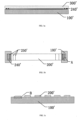
- FIG. 1a is a front view of a mask
- FIG. 1b is a partial top view of the mask shown in FIG. 1a
- the mask comprises a support 100' and at least one mask strip 200', and each mask strip 200' is fixed onto the support 100' by at least one welding spot 240'.
- the mask 100' is disposed on a substrate 300' to be coated, because a height of the welding spot 240' is usually higher than a surface of the mask strip 200', the welding spot 240' will be in direct contact with the substrate 300' and a gap will be formed between the substrate 300' and the mask strip 200', which not only affects fitting closeness between the mask strip 200' and the substrate 300', but also causes evaporation materials to easily accumulate within the gap and hard to remove.
- the substrate 300' is subjected to a large partial pressure, and is apt to crack, thereby causing cracks occurred in the substrate 300'.
- the mask strip 200' when the mask strip 200' is subjected to, for example, an external force, and the like, a corner (such as region A in FIG. 1b ) of the mask strip 200' is easily warped, and the warped portion of the mask strip 200' is apt to cause the substrate 300' to be scratched or the damaged substrate 300' in turn causes the mask strip 200' to be scratched, and the warped portion (e.g., the corner) of the mask strip 200' will also increase a distance between the mask strip 200' and the substrate 300'.
- the mask strip 200' is fixed by the welding spot 240' in a point fixation manner, which is apt to generate a wrinkle 250' in the mask strip 200', and affect the defect-free ratio of evaporation of the substrate 300'.
- FIG. 1c is a side view of the mask shown in FIG. 1a .
- the mask needs to be repaired after the mask strip 200' is replaced, but a portion of the original mask strip 200' fixed by the welding spot 240' needs to be polished, and polishing will cause the support of a corresponding region to be worn.
- a portion of the support 100' located in a region B is worn to a higher degree, resulting in that the mask strip 200' of the region B is not coplanar with other mask strips 200'.
- the repairing operation is performed for a plurality of times, flatness of the region of the support 100' for fixing the mask strip 200' will be affected, which further affects evaporation accuracy of the mask.
- At least one embodiment of the present disclosure provides a mask, and a preparation method and an operation method thereof.
- the mask comprises a support and a mask strip mounted on the support, the mask strip comprising at least two connecting portions connected with the support, and a pattern portion located between the at least two connecting portions, the pattern portion comprising a first outer surface, the connecting portion comprising a second outer surface, the first outer surface and the second outer surface being non-coplanar with each other.
- the substrate to be coated may be provided on the first outer surface; because the second outer surface of the mask strip is not coplanar with the first outer surface, the second outer surface may be distal to the substrate, and both a warped corner of the mask strip and the connector on the second outer surface will not be in contact with the substrate; in this way, the first outer surface of the mask strip may be closely fitted on the substrate, and the defect-free ratio of evaporation of the substrate may be increased.
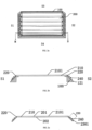
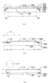
- FIG. 2a is a structural schematic diagram of a mask
- FIG. 2b is a cross-sectional view of the mask of FIG. 2a along M-N
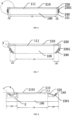
- FIG. 2c is a spatial structure diagram of a mask strip in the mask shown in FIG. 2b
- FIG. 2d is a spatial structure diagram of a support in the mask shown in FIG. 2b .
- a mask comprises: a support 100 and a mask strip 200 mounted on the support 100, the mask strip 200 comprising at least two connecting portions 220 connected with the support 100 and a pattern portion 210 located between the connecting portions 220.
- the connecting portion 220 comprises a mounting region 230, and the mask strip 200 is mounted on the support 100 through a connector 240 in the mounting region 230.
- the mask strip 200 comprises an upper surface 201 and a lower surface 202 opposite to each other, the pattern portion 210 comprises a first outer surface 2101 provided on the upper surface 201, and a surface of the mounting region 230 facing away from the support 100 is a second outer surface 2301, wherein, the second outer surface 2301 and the first outer surface 2101 are non-coplanar with each other, so that the second outer surface 2301 in the mask strip 200 will not be in contact with a substrate, and the connector 240 will not be in contact with the substrate, during evaporation.
- the mask of the above-described structure eliminates a gap between the mask strip 200' and the substrate 300', and implements close fitting between the first outer surface of the mask strip and the surface of the substrate to be coated, which thus increases the defect-free ratio of evaporation of the substrate.
- a mask strip 200 is not limited to comprising two connecting portions 220, and may also comprise more than two connecting portions 220.
- the number of connecting portions 220 comprised in the mask strip 200 may be decided according to actual needs, which will not be limited in the embodiments of the present disclosure.
- the technical solution in the following embodiments of the present disclosure is illustrated, with a case where the mask strip 200 comprises two connecting portions 220 and a pattern portion 210 is provided between the two connecting portions 220 as an example.
- a support 100 comprises a main body (a portion of the support 100 located in a region 110 in FIG. 2d ) and two side portions provided on two opposite sides of the main body (portions of the support 100 in regions 120 in FIG. 2d ).
- the main body 110 may be, for example, of a square frame shape, with a rectangular or square opening in the center, and the opening facilitates exposing the mask strip 200 during evaporation.
- a shape and a size of the opening may be designed according to the number and distribution of the mask strips 200.
- the opening may be of a regular shape such as a round shape, an elliptical shape and a polygonal shape, or may be of an irregular shape.
- a main body and side portions may be of an integrated structure.
- a pattern portion 210 of a mask strip 200 is supported by the main body 110, and two connecting portions 220 of the mask strip 200 are respectively mounted on two side portions 120 of the support 100.
- the main body 110 comprises a first main surface 111 and a second main surface 112 opposite to each other, and a side portion 120 comprises a third outer surface 121.
- the first main surface 111 is connected with the third outer surface 121
- the second outer surface 2301 of the mask strip 200 may be provided with a connector 240 which is configured to fix the mask strip 200 onto the support 100.
- the mask strip 200 can be fixed onto the support 100 in various modes, for example, a riveting mode with a screw, a pin, and the like, or a welding mode such as electrical arc welding, and the like, which will not be limited in the embodiments of the present disclosure.
- the pattern portion 210 of the mask strip 200 has a patterned structure; for example, the pattern portion 210 comprises a plurality of shielding regions and a plurality of non-shielding regions; for example, each of shielding region and each of the non-shielding region may be alternately arranged.
- an evaporation material (a material for evaporation) may pass through the non-shielding region but cannot pass through the shielding region, so after the evaporation material is evaporated and deposited on the substrate, a patterned structure corresponding to the non-shielding region of the mask strip 200 is formed on the substrate.
- a main body of a support 100 may be a frame structure having an opening, side portions are portions extending from sides S 1 and S2 of the frame structure, and the side portions may be used for having a mask strip 200 fixed. It may be understood that, on sides S3 and S4 where the mask strip needs not to be fixed, the support 100 may not be provided with the side portions.
- structures of a support and a side portion depend on relative positional relationship between a second outer surface and a first outer surface on the mask strip 200, which will be described in detail in the embodiments below.
- a second outer surface of a connecting portion is further away from a substrate with respect to a first outer surface of a pattern portion.
- the second outer surface is located on a side facing a lower surface of a plane where the first outer surface is located.
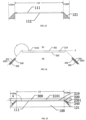
- FIG. 2e is a schematic diagram of spatial distribution of a first outer surface and a second outer surface of a mask strip in a mask provided by the present disclosure (in order to facilitate understanding, only a pattern portion 210 and a mounting region 230 in the mask strip 200, rather than a complete mask strip 200, is shown in FIG. 2e ).
- the first outer surface 2101 of the mask strip 200 is, for example, located in a plane P (a plane where the first outer surface 2101 is located), for example, the plane P may be a horizontal plane, and a side N1 of the horizontal plane P may be provided with a substrate to be coated.
- the second outer surface 2301 is located on a side N2 of the plane P (i.e., a side of the plane P facing a lower surface 202), and the plane P may serve as an interface between the mask strip 200 and the substrate to be coated. Therefore, the second outer surface 2301 and the first outer surface 2101 are non-coplanar with each other; in this case, a connector 240 located on the second outer surface 2301 will not be in contact with the substrate, and a warped corner of the mask strip 200 will not affect the substrate, and thus, the defect-free ratio of evaporation is increased.
- an included angle Q between a first outer surface 2101 and a second outer surface 2301 in a mask strip 200 is greater than or equal to 180 degrees and less than or equal to 360 degrees as an example.
- FIG. 2f is a front view of a mask and a substrate provided by the present disclosure.
- a third outer surface 121 of each side portion 120 of a support 100 may be set as an inclined plane
- two connecting portions 220 of a mask strip 200 are mounted on the inclined plane (the third outer surface 121) through connectors 240, and an included angle Q between a second outer surface 2301 and a first outer surface 2101 in the mask strip 200 is greater than 180 degrees and less than 270 degrees.
- the second outer surface 2301 of the mask strip 200 will not be in contact with a substrate 300 to be coated, and the connector 240 will not be in contact with the substrate 300 to be coated, which implements close fitting between the first outer surface of the mask strip 200 and the substrate 300, and may increase the defect-free ratio of evaporation of the substrate 300.
- each mask strip 200 may comprise a first connecting portion and a second connecting portion, and an included angle between a second outer surface of the first connecting portion and the first outer surface 2101 may be same as or different from an included angle between a second outer surface of the second connecting portion and the first outer surface 2101.
- an included angle between the second outer surface of the first connecting portion and the first outer surface 2101 and the included angle between the second outer surface of the second connecting portion and the first outer surface 2101 are same as each other an example.
- FIG. 2g is a partial structural schematic diagram of a mask provided by the present disclosure.
- a mask strip 200 is fixed onto a support 100 through connectors 240 on second outer surfaces 2301. Because the connector 240 has a certain height, with respect to a mask as shown in FIG. 2g , an included angle Q between a second outer surface 2301 and a first outer surface 2101 may be further set according to the height of a connector 240. As shown in FIG.
- the mask strip 200 is stretched and tightened by the connector 240, so a portion of the mask strip 200 located at a joint between the connecting portion 220 and a pattern portion 210 may be supported by an edge 140 of the support 100 where a main body 110 and the side portion 120 of the support 100 intersect with each other. That is, the edge 140 of the support 100 may support the portion of the mask strip 200 located at the joint between the connecting portion 220 and the pattern portion 210, so as to ensure flatness of the pattern portion 210 of the mask strip 200.
- the edge 140 of the support 100 may support the portion of the mask strip 200 located at the joint between the connecting portion 220 and the pattern portion 210, so as to ensure flatness of the pattern portion 210 of the mask strip 200.
- the mode of fixing the mask strip 200 according to the present disclosure is changed from point fixation to linear fixation (the surface morphology of the pattern portion 210 of the mask strip 200 does not no longer depends on the welding spot 240', but depends on the edge 140), so that a wrinkle 250' in FIG. 1b may be avoided. Even if the wrinkle 250' appears on a second outer surface 2301, the above-described structure (the surface morphology of the pattern portion 210 defined by the edge 140) may also reduce or eliminate extension of the wrinkle toward the pattern portion 210.
- the second outer surface 2301 may be set distal to the position of the edge 140 of the support 100.
- a third outer surface 121 of a side portion 120 of a support 100 may be set in a stair-step shape. In this way, in the procedure of repairing the mask, a repairing operation, for example, a polishing operation will not affect the edge 140, and accuracy of the mask may be ensured.
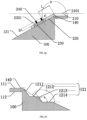
- FIG. 2h is a partial structural schematic diagram of another mask provided by the invention.
- a third outer surface 121 of a side portion 120 of a support 100 is set in a two-stair-step shape and comprises a first sub-surface 1211, a second sub-surface 1212, a third sub-surface 1213 and a fourth sub-surface 1214 that are sequentially connected; the first sub-surface 1211 is connected with a first main surface 111 of a main body 110.
- the second outer surface 2301 may be provided on the second sub-surface 1212, the third sub-surface 1213, or the fourth sub-surface 1214, so that polishing the second outer surface 2301 will not affect an edge 140 of the support 100, while a repairing operation is performed on the mask.
- first sub-surface 1211 and the first main surface 111 of the main body 110 intersect with each other to form a first boundary
- the third sub-surface 1213 and the fourth sub-surface 1214 intersect with each other to form a second boundary
- an included angle c between a plane defined by the first boundary and the second boundary and the fourth sub-surface 1214 is greater than an included angle b between the third sub-surface 1213 and the fourth sub-surface 1214.
- a connecting portion of the mask strip 200 (a portion at a joint between a pattern portion 210 and a connecting portion 220) is supported by both the edge 140 of the support 100 and an edge where the second sub-surface 1212 and the third sub-surface 1213 intersect with each other, which further achieves fixing and tightening effects on the mask strip 200, and reduces or eliminates wrinkles.
- the number of stair-steps is not limited when a third outer surface 121 of a side portion 120 of a support 100 is set in a stair-step shape, and the third outer surface 121 of the side portion 120 of the support 100 may also be set in a one-stair-step shape or a multi-stair-step shape, and the like.
- an edge 140 where a first main surface 111 of a main body 110 and a third outer surface 121 intersect with each other may be rounded or chamfered (as shown in a region of a dotted-line square 140 in FIG. 2h ).
- the edge 140 of a support 100 may be set as a cambered surface having a certain camber (e.g., greater than 0 degree and less than 45 degrees).
- the edge 140 of the support 100 may affect surface morphology of a pattern portion 210 in a mask strip 200, a partial region of the mask strip 200 (e.g., a joint between a pattern portion 210 and a connecting portion 220) will be subjected to a relatively large force if supported by the edge 140, and the edge 140 is set to have a round corner structure so that it has a cambered surface, which may prevent the edge 140 from slashing the mask strip 200 because the edge 140 is too sharp (with partial stress concentrated).
- a partial region of the mask strip 200 e.g., a joint between a pattern portion 210 and a connecting portion 220
- a shape of a third outer surface 121 of a side portion 120 of a support 100 is not limited.
- the third outer surface 121 of the side portion 120 of the support 100 and the second outer surface 2301 of the mask strip 200 are conformal, for example, both are cambered surfaces, or of other curved shapes, and the like.
- FIG. 3 is a structural schematic diagram of a still another mask provided by the present disclosure. As shown in FIG.
- a third outer surface 121 of a side portion 120 of a support 100 is a cambered surface, so that a second outer surface 2301 provided on the third outer surface 121 is also a cambered surface accordingly, as long as an included angle Q between a tangent line of the second outer surface 2301 having a cambered shape and a first outer surface 2101 is greater than 180 degrees and less than 270 degrees, and thus, the second outer surface 2301 is not coplanar with the first outer surface 2101, and the second outer surface 2301 is not in contact with the substrate 300.
- a tangent line of the third outer surface 121 is substantially parallel to the first main surface 111.
- the third outer surface 121 and the first main surface 111 are substantially smoothly connected with each other, which not only prevents an edge 140 from slashing a mask strip 200 because the edge 140 is too sharp (with partial stress concentrated), but also allows both portions of the connecting portion 220 located at the pattern portion 210 and the second outer surface 2301 to be supported by the third outer surface 121, so as to further prevent a wrinkle from extending toward the pattern portion 210, even if the wrinkle appears in the second outer surface 2301.
- FIG. 4 is a structural schematic diagram of a yet another mask of the present disclosure.
- an included angle Q between a second outer surface 2301 and a first outer surface 2101 is 180 degrees, for example, the first outer surface 2101 and the second outer surface 2301 are parallel to each other and provided in different horizontal planes.
- a specific shape of a support 100 may be set according to positional relationship between the first outer surface 2101 and the second outer surface 2301.
- a side portion 120 of a support 100 has a groove.
- a groove D may be provided on a first main surface 111 of the support 100, and a second outer surface 2301 of a mask strip 200 may be provided in the groove D.
- a depth of the groove D may be determined according to actual needs, as long as the depth of the groove D may allow a connector 240 on the second outer surface 2301 not to be in contact with a the substrate to be coated.
- the depth of the groove D is greater than a height of the connector 240.
- the depth of the groove D may be greater than about 10 microns, for example, the depth of the groove D ranges from 10 microns to 20 microns.
- the second outer surface 2301 of the mask strip 200 will not be in contact with the substrate 300 to be coated, and the first outer surface 2101 of the mask strip 200 and the substrate 300 may be closely fitted to each other, so as to increase the defect-free ratio of evaporation of the substrate 300.
- FIG. 5 is a structural schematic diagram of a still another mask provided by the present disclosure.
- an included angle Q between a second outer surface 2301 and a first outer surface 2101 is 360 degrees, for example, the first outer surface 2101 and the second outer surface 2301 are parallel to each other and provided in different horizontal planes.
- a specific shape of a support 100 may be set according to positional relationship between the first outer surface 2101 and the second outer surface 2301.
- a side portion 120 of a support 100 may be in strip-shape.
- a second outer surface 2301 of a mask strip 200 may be provided on a lower surface of the side portion 120 of the support 100 (a surface on a side of the side portion 120 distal to a pattern portion 210).
- the second outer surface 2301 of the mask strip 200 will not be in contact with a substrate 300 to be coated, and the connector 240 on the second outer surface 2301 will not be in contact with the substrate, which may increase the defect-free ratio of evaporation of the substrate 300.
- FIG. 6 is a structural schematic diagram of a yet another mask provided by the present disclosure.
- an included angle Q between a second outer surface 2301 and a first outer surface 2101 of a mask strip 200 is 270 degrees.
- a third outer surface 121 of a side portion 120 of a support 100 may be a vertical plane, i.e., a plane where the third outer surface 121 is located is perpendicular to a first main surface 111 of the support 100.
- the second outer surface 2301 of the mask strip 200 will not be in contact with a substrate 300 to be coated, and the connector 240 on the second outer surface 2301 will not be in contact with the substrate 300, which may increase the defect-free ratio of evaporation of the substrate 300.
- FIG. 7 is a structural schematic diagram of a still another mask provided by the present disclosure.
- an included angle Q between a second outer surface 2301 and a first outer surface 2101 of a mask strip 200 is greater than 270 degrees and less than 360 degrees.
- a third outer surface 121 of a side portion 120 of a support 100 may be a plane which is inclined inward (e.g., inclined from an edge of a main body 110 toward the interior of the main body 110), an included angle between the inclined plane and a first main surface 111 of the support 100 may be between 270 degrees and 360 degrees, and the second outer surface 2301 of the mask strip 200 may be provided on the inclined plane.
- the second outer surface 2301 of the mask strip 200 will not be in contact with the substrate 300 to be coated, and a connector 240 on the second outer surface 2301 will not be in contact with the substrate 300, which may increase the defect-free ratio of evaporation of the substrate 300.
- the surface of the support 100 for having the second outer surface 2301 fixed may not be limited to a flat plane, but may also be of a cambered shape, and the like, and contents of the embodiment shown in FIG. 2h may be referred to for a specific structure thereof, which will not be repeated here in the present disclosure.
- the included angle between the first outer surface 2101 and the second outer surface 2301 of the mask strip 200 will not be limited, and the included angle between the two will not be limited to that between 180 degrees and 360 degrees, as long as the second outer surface 2301 and the first outer surface 2101 are non-coplanar with each other, and the second outer surface 2301 is located on a side of the first outer surface 2101 distal to the surface of the substrate 300 to be coated, so that in the evaporation procedure, the second outer surface will not be in contact with the substrate to be coated, and the defect-free ratio of evaporation of the substrate may be increased.
- FIG. 8 is a structural schematic diagram of a yet another mask provided by the present disclosure.
- a groove E is provided on a first main surface 111 of a support 100, an inclined surface is provided in the groove E, the second outer surface 2301 of the mask strip 200 is provided on the inclined surface; and in a structure of the mask as shown in FIG. 8 , an included angle Q between the second outer surface 2301 and a first outer surface 2101 may be between 0 degree and 180 degrees.
- materials for preparing a support 100 and a mask strip 200 in a mask will not be limited.
- materials for preparing a support 100 and a mask strip 200 may comprise a metal material, so that the mask strip 200 may be fixed onto the support 100, for example, by welding, which is convenient to operate with low process difficulty.
- the present disclosure provides a preparation method of a mask, the preparation method comprising: providing a support and mounting a mask strip on the support; wherein the mask strip comprises at least two connecting portions connected with the support, and a pattern portion located between the at least two connecting portions, the mask strip comprises an upper surface and a lower surface opposite to each other, the pattern portion comprises a first outer surface provided on the upper surface, and the connecting portion comprises a second outer surface provided on the upper surface; the second outer surface and the first outer surface are non-coplanar with each other, and the second outer surface is located on a side of the first outer surface proximal to the lower surface.
- the foregoing embodiments may be referred to for a specific structure of the mask, which will not be repeated here.
- the second outer surface of the mask strip will not be in contact with the substrate, so that a warped corner of the mask strip and a connector (for fixing the mask strip) on the second outer surface, etc., will not affect fitting closeness between the mask strip and the substrate, which may increase the defect-free ratio of evaporation.
- the present disclosure provides an operation method of a mask, the method comprising: placing a the substrate to be coated on a mask, wherein a surface of the substrate to be coated is in contact with a first outer surface of the mask, and the surface of the substrate to be coated is not in contact with a second outer surface of the mask.
- a specific structure of the mask related description in the foregoing embodiments (the embodiments with respect to the mask) may be referred to, and the specific structure of the mask will not be limited in the present disclosure.
- the mask may allow the mask strip and the substrate to be coated to be fitted closely to each other, and in this way, it may be considered that the surface of the substrate to be coated is coplanar with the first outer surface of the pattern portion of the mask strip; because the second outer surface and the first outer surface of the mask strip in the mask are non-coplanar with each other, and the second outer surface is located on a side of the first outer surface proximal to a lower surface of the mask strip, the second outer surface of the mask strip will not be in contact with the surface of the substrate to be coated, which may increase the defect-free ratio of evaporation.
- a surface of a substrate to be coated and a second outer surface are non-coplanar with each other, and an included angle between the two is greater than or equal to 180 degrees and less than or equal to 360 degrees.
- the included angle between the surface of the substrate to be coated and the second outer surface of the mask comprises: 180 degrees, greater than 180 degrees and less than 270 degrees, 270 degrees, greater than 270 degrees and less than 360 degrees, or 360 degrees, and the like.
- the present disclosure provide the mask, the preparation method and the operation method thereof, and may have at least one of advantageous effects below:
Landscapes
- Chemical & Material Sciences (AREA)
- Engineering & Computer Science (AREA)
- Mechanical Engineering (AREA)
- Chemical Kinetics & Catalysis (AREA)
- Materials Engineering (AREA)
- Metallurgy (AREA)
- Organic Chemistry (AREA)
- Physics & Mathematics (AREA)
- General Physics & Mathematics (AREA)
- Physical Vapour Deposition (AREA)
Claims (8)
- Masque utilisé lors de la procédure de production d'un produit électronique, le produit électronique comprenant un substrat à revêtir, le masque comprenant :un support (100) et une bande de masque (200) montée sur le support (100),dans lequel le support (100) comprend un corps principal (110) et deux parties latérales (120) prévues sur des côtés opposés du corps principal (110), le corps principal (110) comprend une première surface principale (111) et une seconde surface principale (112) opposées l'une à l'autre, chaque partie latérale (120) comprend une troisième surface externe (121),caractérisé en ce quela bande de masque (200) comprend au moins deux parties de connexion (220) dont chacune est connectée au support (100), et une partie de motif (210) localisée entre les au moins deux parties de connexion (220), la partie de motif (210) comprenant une première surface externe (2101) et la partie de connexion (220) comprenant une deuxième surface externe (2301) ;dans lequel la première surface externe (2101) et la deuxième surface externe (2301) sont non coplanaires l'une par rapport à l'autre ;dans lequel l'angle inclus (Q) entre la deuxième surface externe (2301) et la première surface externe (2101) est supérieur à 180 degrés et inférieur à 270 degrés, la troisième surface externe (121) de la partie latérale (120) est selon une forme à deux marches d'escalier et comprend une première sous-surface (1211), une deuxième sous-surface (1212), une troisième sous-surface (1213) et une quatrième sous-surface (1214) qui sont connectées séquentiellement, la première sous-surface (1211) est connectée à une première surface principale (111) du corps principal (110), la première sous-surface (1211) et la première surface principale (111) du corps principal (110) s'intersectent l'une l'autre pour former une première frontière, et la troisième sous-surface (1213) et la quatrième sous-surface (1214) s'intersectent l'une l'autre pour former une seconde frontière ; un angle inclus (c) entre un plan défini par la première frontière et la seconde frontière et la quatrième sous-surface (1214) est plus grand qu'un angle inclus (b) entre la troisième sous-surface (1213) et la quatrième sous-surface (1214), et la deuxième surface externe (2301) est fixée sur la troisième sous-surface (1213).
- Masque selon la revendication 1, dans lequel le substrat à revêtir est prévu sur la première surface externe (2101) de la partie de motif (210), et la deuxième surface externe (2301) de la partie de connexion (220) est davantage éloignée du substrat à revêtir par rapport à la première surface externe (2101) de la partie de motif (210).
- Masque selon la revendication 1, dans lequel le support (100) est prévu sur un côté de la bande de masque (200) qui est distal par rapport à la première surface externe (2101), le corps principal (110) est une structure carrée, la partie de motif (210) du masque est supportée par le corps principal (110), les au moins deux parties de connexion (220) de la bande de masque (200) sont respectivement montées sur les deux parties latérales (120), et la première surface principale (111) est connectée à la troisième surface externe (121).
- Masque selon l'une quelconque des revendications 1 à 3, dans lequel les au moins deux parties de connexion (220) comprennent une première partie de connexion et une seconde partie de connexion, et un angle inclus (Q) entre une deuxième surface externe (2301) de la première partie de connexion et la première surface externe (2101) de la partie de motif (210) est égal à un angle inclus (Q) entre une deuxième surface externe (2301) de la seconde partie de connexion et la première surface externe (2101) de la partie de motif (210).
- Masque selon la revendication 3, dans lequel une partie de la bande de masque (200) au niveau d'une jonction entre chaque partie de connexion (220) et la partie de motif (210) est supportée par un bord (140) du support (100) au niveau duquel la première surface principale (111) du corps principal (110) et la troisième surface externe (121) de chaque partie latérale (120) s'intersectent l'une l'autre.
- Masque selon la revendication 5, dans lequel le bord (140) du support (100) au niveau duquel la première surface principale (111) du corps principal (110) et la troisième surface externe (121) de chaque partie latérale (120) s'intersectent l'une l'autre est arrondi ou chanfreiné.
- Procédé de préparation d'un masque utilisé lors de la procédure de production d'un produit électronique, le produit électronique comprenant un substrat à revêtir, le procédé comprenant :la fourniture d'un support (100) et le montage d'une bande de masque (200) sur le support (100) ;dans lequel le support (100) comprend un corps principal (110) et deux parties latérales (120) prévues sur des côtés opposés du corps principal (110), le corps principal (110) comprend une première surface principale (111) et une seconde surface principale (112) opposées l'une à l'autre, chaque partie latérale (120) comprend une troisième surface externe (121),caractérisé en ce quela bande de masque (200) comprend au moins deux parties de connexion (220) dont chacune est connectée au support (100), et une partie de motif (210) localisée entre les au moins deux parties de connexion (220), la partie de motif (210) comprend une première surface externe (2101), et chaque partie de connexion (220) comprend une deuxième surface externe (2301) ; et la deuxième surface externe (2301) et la première surface externe (2101) sont non coplanaires l'une par rapport à l'autre,dans lequel l'angle inclus (Q) entre la deuxième surface externe (2301) et la première surface externe (2101) est supérieur à 180 degrés et inférieur à 270 degrés, la troisième surface externe (121) de la partie latérale (120) est selon une forme à deux marches d'escalier et comprend une première sous-surface (1211), une deuxième sous-surface (1212), une troisième sous-surface (1213) et une quatrième sous-surface (1214) qui sont connectées séquentiellement, la première sous-surface (1211) est connectée à une première surface principale (111) du corps principal (110), la première sous-surface (1211) et la première surface principale (111) du corps principal (110) s'intersectent l'une l'autre pour former une première frontière, et la troisième sous-surface (1213) et la quatrième sous-surface (1214) s'intersectent l'une l'autre pour former une seconde frontière ; un angle inclus (c) entre un plan défini par la première frontière et la seconde frontière et la quatrième sous-surface (1214) est plus grand qu'un angle inclus (b) entre la troisième sous-surface (1213) et la quatrième sous-surface (1214), et la deuxième surface externe (2301) est fixée sur la troisième sous-surface (1213).
- Procédé d'utilisation du masque selon la revendication 1, comprenant :
le positionnement d'un substrat à revêtir sur le masque, dans lequel une surface du substrat à revêtir est en contact avec la première surface externe (2101) du masque, et la surface du substrat à revêtir n'est pas en contact avec la deuxième surface externe du masque (2301).
Applications Claiming Priority (2)
| Application Number | Priority Date | Filing Date | Title |
|---|---|---|---|
| CN201710407553.2A CN108977760B (zh) | 2017-06-02 | 2017-06-02 | 掩模板及其制备方法和使用方法 |
| PCT/CN2017/116953 WO2018218935A1 (fr) | 2017-06-02 | 2017-12-18 | Plaque de masque, procédé de préparation et procédé d'utilisation associés |
Publications (3)
| Publication Number | Publication Date |
|---|---|
| EP3633063A1 EP3633063A1 (fr) | 2020-04-08 |
| EP3633063A4 EP3633063A4 (fr) | 2021-01-20 |
| EP3633063B1 true EP3633063B1 (fr) | 2024-10-02 |
Family
ID=64454410
Family Applications (1)
| Application Number | Title | Priority Date | Filing Date |
|---|---|---|---|
| EP17892059.1A Active EP3633063B1 (fr) | 2017-06-02 | 2017-12-18 | Plaque de masque, procédé de préparation et procédé d'utilisation associés |
Country Status (5)
| Country | Link |
|---|---|
| US (1) | US11746406B2 (fr) |
| EP (1) | EP3633063B1 (fr) |
| JP (1) | JP7092675B2 (fr) |
| CN (1) | CN108977760B (fr) |
| WO (1) | WO2018218935A1 (fr) |
Families Citing this family (8)
| Publication number | Priority date | Publication date | Assignee | Title |
|---|---|---|---|---|
| KR102711116B1 (ko) * | 2019-01-24 | 2024-09-27 | 삼성디스플레이 주식회사 | 표시장치 제조를 위한 마스크유닛 |
| CN109778116B (zh) * | 2019-03-28 | 2021-03-02 | 京东方科技集团股份有限公司 | 一种掩膜版及其制作方法、掩膜版组件 |
| CN110129723B (zh) | 2019-06-27 | 2021-12-10 | 京东方科技集团股份有限公司 | 金属掩膜条、掩膜板框架、金属掩膜板及其焊接方法 |
| CN110331364B (zh) * | 2019-08-02 | 2021-05-07 | 深圳市华星光电半导体显示技术有限公司 | 蒸镀金属掩膜板 |
| KR20220068327A (ko) * | 2020-11-18 | 2022-05-26 | 삼성디스플레이 주식회사 | 마스크 어셈블리 및 그 마스크 어셈블리의 제조 방법 |
| KR20220081406A (ko) * | 2020-12-08 | 2022-06-16 | 삼성디스플레이 주식회사 | 마스크 제조 방법 및 마스크를 포함하는 증착 설비 |
| CN113088877A (zh) * | 2021-04-08 | 2021-07-09 | 京东方科技集团股份有限公司 | 一种掩膜版框架重复使用的方法、掩膜版框架和掩膜版 |
| KR20230077004A (ko) * | 2021-11-24 | 2023-06-01 | 삼성디스플레이 주식회사 | 마스크 조립체 및 이를 포함하는 표시 장치용 증착 장치 |
Family Cites Families (17)
| Publication number | Priority date | Publication date | Assignee | Title |
|---|---|---|---|---|
| JP2000192229A (ja) * | 1998-12-24 | 2000-07-11 | Sony Corp | 真空蒸着法およびディスプレイ製造方法 |
| JP2002175878A (ja) * | 2000-09-28 | 2002-06-21 | Sanyo Electric Co Ltd | 層の形成方法及びカラー発光装置の製造方法 |
| JP4953525B2 (ja) | 2001-07-23 | 2012-06-13 | パナソニック株式会社 | 非水電解質二次電池およびその製造法 |
| US7041412B2 (en) | 2001-07-23 | 2006-05-09 | Matsushita Electric Industrial Co., Ltd. | Non-aqueous electrolyte secondary battery |
| JP2004006257A (ja) | 2002-04-26 | 2004-01-08 | Tohoku Pioneer Corp | 真空蒸着用マスク及びこれを用いて製造された有機elディスプレイパネル |
| JP4944367B2 (ja) | 2004-05-25 | 2012-05-30 | キヤノン株式会社 | マスク構造体の製造方法 |
| JP4860909B2 (ja) * | 2004-05-25 | 2012-01-25 | キヤノン株式会社 | マスク構造体 |
| JP4604593B2 (ja) * | 2004-07-30 | 2011-01-05 | ソニー株式会社 | メタルマスクの製造方法 |
| WO2007073072A1 (fr) * | 2005-12-19 | 2007-06-28 | Doosan Mecatec Co., Ltd. | Appareil de masque destine a effectuer un depot divise sur un substrat, et methode de formation de motifs faisant intervenir cet appareil |
| JP4953424B2 (ja) * | 2006-04-21 | 2012-06-13 | キヤノントッキ株式会社 | 薄膜形成方法 |
| DE102007032228B4 (de) | 2007-07-11 | 2016-01-07 | Gea Tuchenhagen Gmbh | Selbstansaugende Pumpenaggregation |
| US20150299840A1 (en) * | 2012-06-26 | 2015-10-22 | Sharp Kabushiki Kaisha | Mask frame |
| CN104372292B (zh) * | 2013-08-15 | 2018-04-27 | 昆山允升吉光电科技有限公司 | 一种掩模组件 |
| CN204509446U (zh) * | 2014-12-15 | 2015-07-29 | 信利(惠州)智能显示有限公司 | 一种掩膜板固定装置 |
| CN105200370A (zh) * | 2015-10-27 | 2015-12-30 | 唐军 | 可循环使用的掩模板板框及具有它的掩模板 |
| CN205803576U (zh) * | 2016-06-28 | 2016-12-14 | 鄂尔多斯市源盛光电有限责任公司 | 掩膜板 |
| CN106884138A (zh) | 2017-02-15 | 2017-06-23 | 武汉华星光电技术有限公司 | 荫罩组件及荫罩组件的重复使用方法 |
-
2017
- 2017-06-02 CN CN201710407553.2A patent/CN108977760B/zh active Active
- 2017-12-18 WO PCT/CN2017/116953 patent/WO2018218935A1/fr not_active Ceased
- 2017-12-18 US US16/072,359 patent/US11746406B2/en active Active
- 2017-12-18 EP EP17892059.1A patent/EP3633063B1/fr active Active
- 2017-12-18 JP JP2018538726A patent/JP7092675B2/ja not_active Expired - Fee Related
Also Published As
| Publication number | Publication date |
|---|---|
| JP7092675B2 (ja) | 2022-06-28 |
| JP2020521872A (ja) | 2020-07-27 |
| CN108977760B (zh) | 2020-12-08 |
| US11746406B2 (en) | 2023-09-05 |
| CN108977760A (zh) | 2018-12-11 |
| EP3633063A4 (fr) | 2021-01-20 |
| WO2018218935A1 (fr) | 2018-12-06 |
| EP3633063A1 (fr) | 2020-04-08 |
| US20210172047A1 (en) | 2021-06-10 |
Similar Documents
| Publication | Publication Date | Title |
|---|---|---|
| EP3633063B1 (fr) | Plaque de masque, procédé de préparation et procédé d'utilisation associés | |
| TWI678422B (zh) | 附框架蒸鍍遮罩之製造方法、拉張裝置、有機半導體元件之製造裝置及有機半導體元件之製造方法 | |
| JP6423862B2 (ja) | 能動的に位置合わせされるファインメタルマスク | |
| US10301715B2 (en) | Mask for deposition and manufacturing method thereof | |
| WO2018107739A1 (fr) | Cadre de masque, procédé de fabrication de cadre de masque et plaque de masque | |
| WO2014155939A1 (fr) | Unité de cadre de masque, appareil de masque, et procédé de traitement | |
| US11572616B2 (en) | Mask strip, mask plate frame, mask plate and welding method thereof | |
| US11326258B2 (en) | Deposition mask and method of manufacturing the same | |
| KR20040012558A (ko) | 섀도우 마스크 조립체, 섀도우 마스크 조립체 형성 방법 및 기판 상에 패터닝된 재료를 증착시키는 방법 | |
| US20210363628A1 (en) | Mask device, mask plate, and frame | |
| JP2012052155A (ja) | 真空成膜用マスクユニット及びこれを備えた真空成膜装置 | |
| US20150299840A1 (en) | Mask frame | |
| KR20240057092A (ko) | 확장형 마스크와 프레임의 연결체 및 그 제조 방법 | |
| CN112376016B (zh) | 蒸镀掩膜板组件及其制作方法 | |
| CN111235524B (zh) | 掩膜组件和用于制造该掩膜组件的方法 | |
| KR102138800B1 (ko) | 마스크 및 프레임 일체형 마스크 | |
| KR102511834B1 (ko) | 프레임 일체형 마스크 제조용 프레임 및 그 제조 방법 | |
| KR102010815B1 (ko) | 프레임 및 프레임 일체형 마스크 | |
| KR20250021795A (ko) | 확장형 마스크와 프레임의 연결체 및 그 제조 방법 | |
| KR102560422B1 (ko) | 프레임 일체형 마스크에 사용되는 프레임의 크기 설정 방법, 변형량 감소 방법 및 프레임 | |
| KR20190095237A (ko) | 프레임 및 프레임 일체형 마스크 | |
| US20260015708A1 (en) | Mask assembly and method of manufacturing mask assembly | |
| KR102637523B1 (ko) | 마스크 셀 시트부의 변형량 감축 방법, 프레임 일체형 마스크 및 그 제조 방법 | |
| KR20190092840A (ko) | 프레임의 제조 방법 | |
| KR102138797B1 (ko) | 프레임 일체형 마스크 제조 시스템 |
Legal Events
| Date | Code | Title | Description |
|---|---|---|---|
| STAA | Information on the status of an ep patent application or granted ep patent |
Free format text: STATUS: UNKNOWN |
|
| STAA | Information on the status of an ep patent application or granted ep patent |
Free format text: STATUS: THE INTERNATIONAL PUBLICATION HAS BEEN MADE |
|
| PUAI | Public reference made under article 153(3) epc to a published international application that has entered the european phase |
Free format text: ORIGINAL CODE: 0009012 |
|
| STAA | Information on the status of an ep patent application or granted ep patent |
Free format text: STATUS: REQUEST FOR EXAMINATION WAS MADE |
|
| 17P | Request for examination filed |
Effective date: 20180723 |
|
| AK | Designated contracting states |
Kind code of ref document: A1 Designated state(s): AL AT BE BG CH CY CZ DE DK EE ES FI FR GB GR HR HU IE IS IT LI LT LU LV MC MK MT NL NO PL PT RO RS SE SI SK SM TR |
|
| AX | Request for extension of the european patent |
Extension state: BA ME |
|
| DAV | Request for validation of the european patent (deleted) | ||
| DAX | Request for extension of the european patent (deleted) | ||
| A4 | Supplementary search report drawn up and despatched |
Effective date: 20201221 |
|
| RIC1 | Information provided on ipc code assigned before grant |
Ipc: H01L 51/00 20060101ALI20201215BHEP Ipc: C23C 14/04 20060101AFI20201215BHEP Ipc: C23C 14/24 20060101ALI20201215BHEP Ipc: H01L 21/68 20060101ALI20201215BHEP |
|
| RIC1 | Information provided on ipc code assigned before grant |
Ipc: H01L 21/68 20060101ALI20240410BHEP Ipc: H10K 71/16 20230101ALI20240410BHEP Ipc: C23C 14/04 20060101AFI20240410BHEP |
|
| GRAP | Despatch of communication of intention to grant a patent |
Free format text: ORIGINAL CODE: EPIDOSNIGR1 |
|
| STAA | Information on the status of an ep patent application or granted ep patent |
Free format text: STATUS: GRANT OF PATENT IS INTENDED |
|
| INTG | Intention to grant announced |
Effective date: 20240521 |
|
| GRAS | Grant fee paid |
Free format text: ORIGINAL CODE: EPIDOSNIGR3 |
|
| GRAA | (expected) grant |
Free format text: ORIGINAL CODE: 0009210 |
|
| STAA | Information on the status of an ep patent application or granted ep patent |
Free format text: STATUS: THE PATENT HAS BEEN GRANTED |
|
| AK | Designated contracting states |
Kind code of ref document: B1 Designated state(s): AL AT BE BG CH CY CZ DE DK EE ES FI FR GB GR HR HU IE IS IT LI LT LU LV MC MK MT NL NO PL PT RO RS SE SI SK SM TR |
|
| REG | Reference to a national code |
Ref country code: GB Ref legal event code: FG4D |
|
| REG | Reference to a national code |
Ref country code: CH Ref legal event code: EP |
|
| REG | Reference to a national code |
Ref country code: DE Ref legal event code: R096 Ref document number: 602017085273 Country of ref document: DE |
|
| REG | Reference to a national code |
Ref country code: IE Ref legal event code: FG4D |
|
| REG | Reference to a national code |
Ref country code: LT Ref legal event code: MG9D |
|
| REG | Reference to a national code |
Ref country code: NL Ref legal event code: MP Effective date: 20241002 |
|
| REG | Reference to a national code |
Ref country code: AT Ref legal event code: MK05 Ref document number: 1728546 Country of ref document: AT Kind code of ref document: T Effective date: 20241002 |
|
| PG25 | Lapsed in a contracting state [announced via postgrant information from national office to epo] |
Ref country code: NL Free format text: LAPSE BECAUSE OF FAILURE TO SUBMIT A TRANSLATION OF THE DESCRIPTION OR TO PAY THE FEE WITHIN THE PRESCRIBED TIME-LIMIT Effective date: 20241002 |
|
| PG25 | Lapsed in a contracting state [announced via postgrant information from national office to epo] |
Ref country code: NL Free format text: LAPSE BECAUSE OF FAILURE TO SUBMIT A TRANSLATION OF THE DESCRIPTION OR TO PAY THE FEE WITHIN THE PRESCRIBED TIME-LIMIT Effective date: 20241002 |
|
| PG25 | Lapsed in a contracting state [announced via postgrant information from national office to epo] |
Ref country code: PT Free format text: LAPSE BECAUSE OF FAILURE TO SUBMIT A TRANSLATION OF THE DESCRIPTION OR TO PAY THE FEE WITHIN THE PRESCRIBED TIME-LIMIT Effective date: 20250203 Ref country code: IS Free format text: LAPSE BECAUSE OF FAILURE TO SUBMIT A TRANSLATION OF THE DESCRIPTION OR TO PAY THE FEE WITHIN THE PRESCRIBED TIME-LIMIT Effective date: 20250202 Ref country code: HR Free format text: LAPSE BECAUSE OF FAILURE TO SUBMIT A TRANSLATION OF THE DESCRIPTION OR TO PAY THE FEE WITHIN THE PRESCRIBED TIME-LIMIT Effective date: 20241002 |
|
| PG25 | Lapsed in a contracting state [announced via postgrant information from national office to epo] |
Ref country code: FI Free format text: LAPSE BECAUSE OF FAILURE TO SUBMIT A TRANSLATION OF THE DESCRIPTION OR TO PAY THE FEE WITHIN THE PRESCRIBED TIME-LIMIT Effective date: 20241002 |
|
| PG25 | Lapsed in a contracting state [announced via postgrant information from national office to epo] |
Ref country code: BG Free format text: LAPSE BECAUSE OF FAILURE TO SUBMIT A TRANSLATION OF THE DESCRIPTION OR TO PAY THE FEE WITHIN THE PRESCRIBED TIME-LIMIT Effective date: 20241002 |
|
| PG25 | Lapsed in a contracting state [announced via postgrant information from national office to epo] |
Ref country code: ES Free format text: LAPSE BECAUSE OF FAILURE TO SUBMIT A TRANSLATION OF THE DESCRIPTION OR TO PAY THE FEE WITHIN THE PRESCRIBED TIME-LIMIT Effective date: 20241002 |
|
| PG25 | Lapsed in a contracting state [announced via postgrant information from national office to epo] |
Ref country code: NO Free format text: LAPSE BECAUSE OF FAILURE TO SUBMIT A TRANSLATION OF THE DESCRIPTION OR TO PAY THE FEE WITHIN THE PRESCRIBED TIME-LIMIT Effective date: 20250102 |
|
| PG25 | Lapsed in a contracting state [announced via postgrant information from national office to epo] |
Ref country code: LV Free format text: LAPSE BECAUSE OF FAILURE TO SUBMIT A TRANSLATION OF THE DESCRIPTION OR TO PAY THE FEE WITHIN THE PRESCRIBED TIME-LIMIT Effective date: 20241002 Ref country code: AT Free format text: LAPSE BECAUSE OF FAILURE TO SUBMIT A TRANSLATION OF THE DESCRIPTION OR TO PAY THE FEE WITHIN THE PRESCRIBED TIME-LIMIT Effective date: 20241002 Ref country code: GR Free format text: LAPSE BECAUSE OF FAILURE TO SUBMIT A TRANSLATION OF THE DESCRIPTION OR TO PAY THE FEE WITHIN THE PRESCRIBED TIME-LIMIT Effective date: 20250103 |
|
| PG25 | Lapsed in a contracting state [announced via postgrant information from national office to epo] |
Ref country code: CZ Free format text: LAPSE BECAUSE OF FAILURE TO SUBMIT A TRANSLATION OF THE DESCRIPTION OR TO PAY THE FEE WITHIN THE PRESCRIBED TIME-LIMIT Effective date: 20241002 Ref country code: PL Free format text: LAPSE BECAUSE OF FAILURE TO SUBMIT A TRANSLATION OF THE DESCRIPTION OR TO PAY THE FEE WITHIN THE PRESCRIBED TIME-LIMIT Effective date: 20241002 |
|
| PG25 | Lapsed in a contracting state [announced via postgrant information from national office to epo] |
Ref country code: RS Free format text: LAPSE BECAUSE OF FAILURE TO SUBMIT A TRANSLATION OF THE DESCRIPTION OR TO PAY THE FEE WITHIN THE PRESCRIBED TIME-LIMIT Effective date: 20250102 |
|
| PG25 | Lapsed in a contracting state [announced via postgrant information from national office to epo] |
Ref country code: SM Free format text: LAPSE BECAUSE OF FAILURE TO SUBMIT A TRANSLATION OF THE DESCRIPTION OR TO PAY THE FEE WITHIN THE PRESCRIBED TIME-LIMIT Effective date: 20241002 |
|
| REG | Reference to a national code |
Ref country code: DE Ref legal event code: R097 Ref document number: 602017085273 Country of ref document: DE |
|
| PG25 | Lapsed in a contracting state [announced via postgrant information from national office to epo] |
Ref country code: MC Free format text: LAPSE BECAUSE OF FAILURE TO SUBMIT A TRANSLATION OF THE DESCRIPTION OR TO PAY THE FEE WITHIN THE PRESCRIBED TIME-LIMIT Effective date: 20241002 |
|
| PG25 | Lapsed in a contracting state [announced via postgrant information from national office to epo] |
Ref country code: DK Free format text: LAPSE BECAUSE OF FAILURE TO SUBMIT A TRANSLATION OF THE DESCRIPTION OR TO PAY THE FEE WITHIN THE PRESCRIBED TIME-LIMIT Effective date: 20241002 |
|
| PG25 | Lapsed in a contracting state [announced via postgrant information from national office to epo] |
Ref country code: EE Free format text: LAPSE BECAUSE OF FAILURE TO SUBMIT A TRANSLATION OF THE DESCRIPTION OR TO PAY THE FEE WITHIN THE PRESCRIBED TIME-LIMIT Effective date: 20241002 |
|
| PG25 | Lapsed in a contracting state [announced via postgrant information from national office to epo] |
Ref country code: RO Free format text: LAPSE BECAUSE OF FAILURE TO SUBMIT A TRANSLATION OF THE DESCRIPTION OR TO PAY THE FEE WITHIN THE PRESCRIBED TIME-LIMIT Effective date: 20241002 |
|
| PG25 | Lapsed in a contracting state [announced via postgrant information from national office to epo] |
Ref country code: SK Free format text: LAPSE BECAUSE OF FAILURE TO SUBMIT A TRANSLATION OF THE DESCRIPTION OR TO PAY THE FEE WITHIN THE PRESCRIBED TIME-LIMIT Effective date: 20241002 |
|
| PG25 | Lapsed in a contracting state [announced via postgrant information from national office to epo] |
Ref country code: IT Free format text: LAPSE BECAUSE OF FAILURE TO SUBMIT A TRANSLATION OF THE DESCRIPTION OR TO PAY THE FEE WITHIN THE PRESCRIBED TIME-LIMIT Effective date: 20241002 |
|
| REG | Reference to a national code |
Ref country code: CH Ref legal event code: PL |
|
| PLBE | No opposition filed within time limit |
Free format text: ORIGINAL CODE: 0009261 |
|
| STAA | Information on the status of an ep patent application or granted ep patent |
Free format text: STATUS: NO OPPOSITION FILED WITHIN TIME LIMIT |
|
| PG25 | Lapsed in a contracting state [announced via postgrant information from national office to epo] |
Ref country code: LU Free format text: LAPSE BECAUSE OF NON-PAYMENT OF DUE FEES Effective date: 20241218 |
|
| PG25 | Lapsed in a contracting state [announced via postgrant information from national office to epo] |
Ref country code: SE Free format text: LAPSE BECAUSE OF FAILURE TO SUBMIT A TRANSLATION OF THE DESCRIPTION OR TO PAY THE FEE WITHIN THE PRESCRIBED TIME-LIMIT Effective date: 20241002 |
|
| 26N | No opposition filed |
Effective date: 20250703 |
|
| GBPC | Gb: european patent ceased through non-payment of renewal fee |
Effective date: 20250102 |
|
| REG | Reference to a national code |
Ref country code: BE Ref legal event code: MM Effective date: 20241231 |
|
| PG25 | Lapsed in a contracting state [announced via postgrant information from national office to epo] |
Ref country code: BE Free format text: LAPSE BECAUSE OF NON-PAYMENT OF DUE FEES Effective date: 20241231 Ref country code: GB Free format text: LAPSE BECAUSE OF NON-PAYMENT OF DUE FEES Effective date: 20250102 |
|
| PG25 | Lapsed in a contracting state [announced via postgrant information from national office to epo] |
Ref country code: FR Free format text: LAPSE BECAUSE OF NON-PAYMENT OF DUE FEES Effective date: 20241231 |
|
| PG25 | Lapsed in a contracting state [announced via postgrant information from national office to epo] |
Ref country code: CH Free format text: LAPSE BECAUSE OF NON-PAYMENT OF DUE FEES Effective date: 20241231 |
|
| PG25 | Lapsed in a contracting state [announced via postgrant information from national office to epo] |
Ref country code: IE Free format text: LAPSE BECAUSE OF NON-PAYMENT OF DUE FEES Effective date: 20241218 |
|
| PGFP | Annual fee paid to national office [announced via postgrant information from national office to epo] |
Ref country code: DE Payment date: 20251211 Year of fee payment: 9 |