EP3633736A1 - Perowskit-silizium-tandemsolarzelle und herstellungsverfahren - Google Patents
Perowskit-silizium-tandemsolarzelle und herstellungsverfahren Download PDFInfo
- Publication number
- EP3633736A1 EP3633736A1 EP18810525.8A EP18810525A EP3633736A1 EP 3633736 A1 EP3633736 A1 EP 3633736A1 EP 18810525 A EP18810525 A EP 18810525A EP 3633736 A1 EP3633736 A1 EP 3633736A1
- Authority
- EP
- European Patent Office
- Prior art keywords
- solar cell
- layer
- texture
- etching
- substrate
- Prior art date
- Legal status (The legal status is an assumption and is not a legal conclusion. Google has not performed a legal analysis and makes no representation as to the accuracy of the status listed.)
- Granted
Links
Images



Classifications
-
- H—ELECTRICITY
- H10—SEMICONDUCTOR DEVICES; ELECTRIC SOLID-STATE DEVICES NOT OTHERWISE PROVIDED FOR
- H10F—INORGANIC SEMICONDUCTOR DEVICES SENSITIVE TO INFRARED RADIATION, LIGHT, ELECTROMAGNETIC RADIATION OF SHORTER WAVELENGTH OR CORPUSCULAR RADIATION
- H10F77/00—Constructional details of devices covered by this subclass
- H10F77/70—Surface textures, e.g. pyramid structures
- H10F77/707—Surface textures, e.g. pyramid structures of the substrates or of layers on substrates, e.g. textured ITO layer on a glass substrate
-
- H—ELECTRICITY
- H10—SEMICONDUCTOR DEVICES; ELECTRIC SOLID-STATE DEVICES NOT OTHERWISE PROVIDED FOR
- H10F—INORGANIC SEMICONDUCTOR DEVICES SENSITIVE TO INFRARED RADIATION, LIGHT, ELECTROMAGNETIC RADIATION OF SHORTER WAVELENGTH OR CORPUSCULAR RADIATION
- H10F10/00—Individual photovoltaic cells, e.g. solar cells
- H10F10/10—Individual photovoltaic cells, e.g. solar cells having potential barriers
- H10F10/19—Photovoltaic cells having multiple potential barriers of different types, e.g. tandem cells having both PN and PIN junctions
-
- H—ELECTRICITY
- H01—ELECTRIC ELEMENTS
- H01G—CAPACITORS; CAPACITORS, RECTIFIERS, DETECTORS, SWITCHING DEVICES, LIGHT-SENSITIVE OR TEMPERATURE-SENSITIVE DEVICES OF THE ELECTROLYTIC TYPE
- H01G9/00—Electrolytic capacitors, rectifiers, detectors, switching devices, light-sensitive or temperature-sensitive devices; Processes of their manufacture
- H01G9/20—Light-sensitive devices
- H01G9/2004—Light-sensitive devices characterised by the electrolyte, e.g. comprising an organic electrolyte
- H01G9/2009—Solid electrolytes
-
- H—ELECTRICITY
- H10—SEMICONDUCTOR DEVICES; ELECTRIC SOLID-STATE DEVICES NOT OTHERWISE PROVIDED FOR
- H10F—INORGANIC SEMICONDUCTOR DEVICES SENSITIVE TO INFRARED RADIATION, LIGHT, ELECTROMAGNETIC RADIATION OF SHORTER WAVELENGTH OR CORPUSCULAR RADIATION
- H10F10/00—Individual photovoltaic cells, e.g. solar cells
- H10F10/10—Individual photovoltaic cells, e.g. solar cells having potential barriers
- H10F10/16—Photovoltaic cells having only PN heterojunction potential barriers
- H10F10/161—Photovoltaic cells having only PN heterojunction potential barriers comprising multiple PN heterojunctions, e.g. tandem cells
-
- H—ELECTRICITY
- H10—SEMICONDUCTOR DEVICES; ELECTRIC SOLID-STATE DEVICES NOT OTHERWISE PROVIDED FOR
- H10F—INORGANIC SEMICONDUCTOR DEVICES SENSITIVE TO INFRARED RADIATION, LIGHT, ELECTROMAGNETIC RADIATION OF SHORTER WAVELENGTH OR CORPUSCULAR RADIATION
- H10F71/00—Manufacture or treatment of devices covered by this subclass
-
- H—ELECTRICITY
- H10—SEMICONDUCTOR DEVICES; ELECTRIC SOLID-STATE DEVICES NOT OTHERWISE PROVIDED FOR
- H10F—INORGANIC SEMICONDUCTOR DEVICES SENSITIVE TO INFRARED RADIATION, LIGHT, ELECTROMAGNETIC RADIATION OF SHORTER WAVELENGTH OR CORPUSCULAR RADIATION
- H10F77/00—Constructional details of devices covered by this subclass
- H10F77/70—Surface textures, e.g. pyramid structures
- H10F77/703—Surface textures, e.g. pyramid structures of the semiconductor bodies, e.g. textured active layers
-
- H—ELECTRICITY
- H10—SEMICONDUCTOR DEVICES; ELECTRIC SOLID-STATE DEVICES NOT OTHERWISE PROVIDED FOR
- H10K—ORGANIC ELECTRIC SOLID-STATE DEVICES
- H10K30/00—Organic devices sensitive to infrared radiation, light, electromagnetic radiation of shorter wavelength or corpuscular radiation
- H10K30/50—Photovoltaic [PV] devices
- H10K30/57—Photovoltaic [PV] devices comprising multiple junctions, e.g. tandem PV cells
-
- H—ELECTRICITY
- H10—SEMICONDUCTOR DEVICES; ELECTRIC SOLID-STATE DEVICES NOT OTHERWISE PROVIDED FOR
- H10K—ORGANIC ELECTRIC SOLID-STATE DEVICES
- H10K85/00—Organic materials used in the body or electrodes of devices covered by this subclass
- H10K85/50—Organic perovskites; Hybrid organic-inorganic perovskites [HOIP], e.g. CH3NH3PbI3
-
- H—ELECTRICITY
- H10—SEMICONDUCTOR DEVICES; ELECTRIC SOLID-STATE DEVICES NOT OTHERWISE PROVIDED FOR
- H10K—ORGANIC ELECTRIC SOLID-STATE DEVICES
- H10K30/00—Organic devices sensitive to infrared radiation, light, electromagnetic radiation of shorter wavelength or corpuscular radiation
- H10K30/10—Organic devices sensitive to infrared radiation, light, electromagnetic radiation of shorter wavelength or corpuscular radiation comprising heterojunctions between organic semiconductors and inorganic semiconductors
- H10K30/15—Sensitised wide-bandgap semiconductor devices, e.g. dye-sensitised TiO2
- H10K30/151—Sensitised wide-bandgap semiconductor devices, e.g. dye-sensitised TiO2 the wide bandgap semiconductor comprising titanium oxide, e.g. TiO2
-
- H—ELECTRICITY
- H10—SEMICONDUCTOR DEVICES; ELECTRIC SOLID-STATE DEVICES NOT OTHERWISE PROVIDED FOR
- H10K—ORGANIC ELECTRIC SOLID-STATE DEVICES
- H10K30/00—Organic devices sensitive to infrared radiation, light, electromagnetic radiation of shorter wavelength or corpuscular radiation
- H10K30/50—Photovoltaic [PV] devices
-
- Y—GENERAL TAGGING OF NEW TECHNOLOGICAL DEVELOPMENTS; GENERAL TAGGING OF CROSS-SECTIONAL TECHNOLOGIES SPANNING OVER SEVERAL SECTIONS OF THE IPC; TECHNICAL SUBJECTS COVERED BY FORMER USPC CROSS-REFERENCE ART COLLECTIONS [XRACs] AND DIGESTS
- Y02—TECHNOLOGIES OR APPLICATIONS FOR MITIGATION OR ADAPTATION AGAINST CLIMATE CHANGE
- Y02E—REDUCTION OF GREENHOUSE GAS [GHG] EMISSIONS, RELATED TO ENERGY GENERATION, TRANSMISSION OR DISTRIBUTION
- Y02E10/00—Energy generation through renewable energy sources
- Y02E10/50—Photovoltaic [PV] energy
- Y02E10/542—Dye sensitized solar cells
-
- Y—GENERAL TAGGING OF NEW TECHNOLOGICAL DEVELOPMENTS; GENERAL TAGGING OF CROSS-SECTIONAL TECHNOLOGIES SPANNING OVER SEVERAL SECTIONS OF THE IPC; TECHNICAL SUBJECTS COVERED BY FORMER USPC CROSS-REFERENCE ART COLLECTIONS [XRACs] AND DIGESTS
- Y02—TECHNOLOGIES OR APPLICATIONS FOR MITIGATION OR ADAPTATION AGAINST CLIMATE CHANGE
- Y02E—REDUCTION OF GREENHOUSE GAS [GHG] EMISSIONS, RELATED TO ENERGY GENERATION, TRANSMISSION OR DISTRIBUTION
- Y02E10/00—Energy generation through renewable energy sources
- Y02E10/50—Photovoltaic [PV] energy
- Y02E10/549—Organic PV cells
-
- Y—GENERAL TAGGING OF NEW TECHNOLOGICAL DEVELOPMENTS; GENERAL TAGGING OF CROSS-SECTIONAL TECHNOLOGIES SPANNING OVER SEVERAL SECTIONS OF THE IPC; TECHNICAL SUBJECTS COVERED BY FORMER USPC CROSS-REFERENCE ART COLLECTIONS [XRACs] AND DIGESTS
- Y02—TECHNOLOGIES OR APPLICATIONS FOR MITIGATION OR ADAPTATION AGAINST CLIMATE CHANGE
- Y02P—CLIMATE CHANGE MITIGATION TECHNOLOGIES IN THE PRODUCTION OR PROCESSING OF GOODS
- Y02P70/00—Climate change mitigation technologies in the production process for final industrial or consumer products
- Y02P70/50—Manufacturing or production processes characterised by the final manufactured product
Definitions
- the present disclosure relates to a tandem solar cell, and more particularly, to a monolithic tandem solar cell in which a perovskite solar cell is uniformly stacked on and bonded to a textured silicon solar cell and a method of manufacturing the same.
- Crystalline silicon (c-Si) solar cells are representative single-junction solar cells which are currently widely used as commercial solar cells.
- c-Si Crystalline silicon
- FIG. 1 is a schematic cross-sectional view of a two-terminal tandem solar cell, which is a common type of tandem solar cell.
- a single-junction solar cell including an absorption layer having a relatively large band gap and a single-junction solar cell including an absorption layer having a relatively small band gap are tunnel-junctioned through a inter-layer.
- Perovskite/crystalline silicon tandem solar cells have been attracting attention as potential candidates for achieving a photovoltaic efficiency of more than 30%, where a single junction solar cell including an absorption layer having a relatively large bandgap among various types of two-terminal tandem solar cells is used as a perovskite solar cell and a single junction solar cell including an absorption layer having a relatively small bandgap is used as a crystalline silicon solar cell.
- a textured structure having both valley shapes and peak shapes is formed on a crystalline silicon substrate surface in order to reduce the reflectance of incident light and thereby improve light efficiency.
- a perovskite absorption layer subsequently formed on the silicon substrate is formed using a thin-film process such as a liquid solution process, a chemical deposition process, or a physical deposition process.
- the texture has a geometrically fine pitch in that the distance between peaks is several micrometers to several tens of micrometers.
- a subsequent process is a thin-film process, in order to form a porous perovskite absorption layer, before particles that have reached the substrate are stacked in stable valley positions, it is required that other subsequent particles reach and become deposited on the textured substrate.
- the fine pitch of the texture makes the uniform crystallization conversion of the perovskite absorption layer difficult.
- an inclined surface of the texture forms a geometric inclination angle of about 55 degrees relative to the horizontal direction of the ⁇ 100 ⁇ substrate due to the chemical stability of a ⁇ 111 ⁇ plane.
- Such a large inclination angle impedes the formation of a perovskite absorption layer at the inclined portions, and as a result, the thickness of the perovskite absorption layer may become non-uniform in that the thickness becomes smaller at peaks and inclined portions than near valleys.
- the present disclosure is directed to providing a tandem solar cell including a substrate on which a texture having both valley shapes and peak shapes is formed in order to reduce the reflectance of vertically incident light as well as obliquely changing the direction of light incidence, wherein the valley and peak portions of the texture have a round shape due to a rounding process.
- the present disclosure is directed to improving, by increasing the radii of curvature of a texture of a substrate, the uniformity of a inter-layer (also referred to as a tunnel inter-layer or an intermediate layer) and a perovskite absorption layer that are formed on the texture.
- a inter-layer also referred to as a tunnel inter-layer or an intermediate layer
- a perovskite absorption layer that are formed on the texture.
- a uniform perovskite absorption layer provides a tandem solar cell which includes: a substrate on which a texture having valley and peak shapes is formed; and a perovskite absorption layer formed on the substrate, wherein the valley portions and the peak portions of the texture have a round shape.
- tandem solar cell in which the radii of curvature of the valley portions are different from the radii of curvature of the peak portions.
- tandem solar cell in which absolute values of the radii of curvature of the valley portions are greater than or equal to absolute values of the radii of curvature of the peak portions.
- tandem solar cell in which the radii of curvature of the valley portions are in a range of 0.05 to 50 ⁇ m.
- tandem solar cell in which inclined surfaces connecting valley portions to peak portions form an angle of less than 55 degrees relative to the planar direction of the substrate.
- tandem solar cell in which, in the texture, an average distance between valleys or between centers of flat portions is larger than an average distance between peaks.
- a tandem solar cell in which a thickness of the perovskite absorption layer formed at the valley portions of a texture differs from thicknesses at the peak portions and the inclined surfaces of the texture by at most 10%.
- a method of manufacturing a tandem solar cell that includes: forming a texture having valley and peak shapes on a substrate; performing a rounding process on valley and peak portions of the texture; and forming a perovskite absorption layer on the substrate.
- a tandem solar cell in which the forming of the texture on the substrate is carried out by anisotropic etching.
- a method of manufacturing a tandem solar cell in which the rounding process is isotropic etching that is carried out by any one of wet etching, sputtering etching, reactive ion etching, and vapor-phase etching.
- a method of manufacturing a tandem solar cell in which the rounding process is etching carried out using an etching solution in which hydrofluoric acid and nitric acid are mixed in a ratio of 1:(10 to 80).
- a method of manufacturing a tandem solar cell which may further include forming a inter-layer before the forming of the perovskite absorption layer.
- a tandem solar cell in which the perovskite absorption layer is formed by physical vapor deposition or chemical vapor deposition.
- a tandem solar cell in which the valley and peak portions of a texture are rounded and a method of manufacturing the same.
- the present disclosure allows a perovskite absorption layer to be uniformly formed and converted at valley portions of a texture, there are effects of not only uniformly improving tandem solar cell efficiency throughout a panel but also stably forming a inter-layer at peak portions.
- isotropic etching prevents etching from being localized to peak portions which preferentially react with an etching composition as well as promoting etching towards valley portions.
- the isotropic etching of the present disclosure can form a texture in which the absolute values of the radii of curvature of the valley portions are greater than or equal to the absolute values of the radii of curvature of the peak portions. Since the isotropic etching method of the present disclosure allows a perovskite absorption layer to be stably converted at valley portions while maintaining the frame of the texture intact, the light absorption and the reliability of a tandem solar cell can be improved.
- the inclination angle of the inclined surfaces connecting valley portions to peak portions is reduced through rounding. Since a difference in the thickness of a perovskite absorption layer formed on the texture at the valley portions, the peak portions, and the inclined portions can thus be reduced by the etching method of the present disclosure, tandem solar cell efficiency can be uniformly improved throughout a panel.
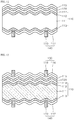
- FIG. 2 is a cross-sectional view of a tandem solar cell according to one embodiment of the present disclosure
- FIG. 3 is a detailed cross-sectional view of a perovskite solar cell which is the second solar cell of FIG. 2 .
- a tandem solar cell according to a first embodiment of the present disclosure has a structure of a two-terminal tandem solar cell in which a perovskite solar cell 120, as a second solar cell including an absorption layer having a relatively large band gap, and a silicon solar cell 110, as a first solar cell including an absorption layer having a relatively small band gap, are directly tunnel-junctioned through a inter-layer 114.
- the tandem solar cell Accordingly, among light incident on the tandem solar cell, light in a short-wavelength region is absorbed by the perovskite solar cell 120 which is the second solar cell disposed in an upper portion, whereby electrical charges are generated, and light in a long-wavelength region is transmitted through the second solar cell 120 and absorbed by the silicon solar cell 110 which is the first solar cell disposed in a lower portion, whereby electrical charges are generated.
- the threshold wavelength can be shifted toward longer wavelengths, and therefore, the tandem solar cell having the above-described structure has the advantage that the range of wavelengths absorbed by the entire solar cell can be broadened.
- the above-described tandem solar cell includes a silicon solar cell 110 as a first solar cell, a perovskite solar cell 120 as a second solar cell, a inter-layer 114, a first electrode 140, and a second electrode 130.
- the first solar cell 110 of the present disclosure may be implemented as a heterojunction silicon solar cell or homojunction silicon solar cell.
- the first solar cell 110 when the first solar cell 110 is a heterojunction silicon solar cell, the first solar cell 110 may have a structure in which very thin amorphous intrinsic silicon (i a-Si:H) as a passivation layer is first formed on the front and rear sides of an n-type crystalline silicon substrate, a p-type high-concentration amorphous silicon (p a-Si:H) layer as an emitter layer 112 is formed on a second surface which is on the front side, and, on a first surface which is the rear side, a high-concentration amorphous silicon (n+ a-Si:H) layer as a back surface field (hereinafter abbreviated as BSF) layer 113 is formed.
- a back surface field hereinafter abbreviated as BSF
- An amorphous silicon layer has an advantage of being a material which not only has an energy band gap of about 0.6 to 0.7 eV larger than an energy band gap of a crystalline silicon layer which is about 1.1 eV, but also can be formed with a very small thickness during a deposition process. Due to the advantageous features of the amorphous silicon layer, as light absorption loss in a short-wavelength region is minimized, a light utilization rate can be ultimately increased, and a high open-circuit voltage and an effective back surface field can be attained.
- a hydrogenated intrinsic amorphous silicon (i a-Si:H) layer is used as the intrinsic amorphous silicon layer. This is because by entering the amorphous silicon due to a hydrogenation reaction, hydrogen can reduce a dangling bond state of the amorphous silicon and a localized energy state within an energy band gap.
- a temperature of a subsequent processe is limited to 250 °C or less and more preferably 200 °C or less. This is because the hydrogen bonding inside amorphous silicon breaks at a process temperature exceeding 200 °C.
- the first solar cell 110 of the present disclosure may also be implemented as a homojunction crystalline silicon solar cell.
- the first solar cell 110 has an emitter layer 112 disposed on a second surface of a crystalline silicon substrate 111.
- the first solar cell 110 may further have a BSF layer 113 disposed on a first surface of the crystalline silicon substrate 111. That is, the first solar cell 110 may have a two-layer structure in which a silicon substrate 111 and an emitter layer 112 are sequentially stacked.
- the first solar cell 110 may also have a three-layer structure in which a BSF layer 113, a silicon substrate 111, and an emitter layer 112 are sequentially stacked.
- a homojunction crystalline silicon solar cell 110 can be realized.
- the crystalline silicon substrate 111 is an n-type monocrystalline silicon substrate
- a semiconductor layer doped with p-type impurities is used as the emitter layer 112 and a semiconductor layer doped with n-type impurities is used as the BSF layer 113.
- the BSF layer 113 may be an n+-type semiconductor layer which is doped at a higher concentration than the concentration of the n-type impurities used for doping the crystalline silicon substrate 111.
- the crystalline silicon substrate 111 of the first solar cell 110 has, in at least one of first and second surfaces thereof, a textured structure having valley and peak shapes.
- a textured structure When such a textured structure is applied to a first surface of the crystalline silicon substrate 111, a BSF layer 113 subsequently disposed on the first surface of the crystalline silicon substrate 111 also acquires the textured structure.
- an emitter layer 112, a inter-layer 114, and a second solar cell 120 which are sequentially provided on the second surface of the crystalline silicon substrate 111 also acquire the textured structure.
- the reflectance at an interface between the inter-layer 114 and the first solar cell 110 can be reduced.
- light having a long wavelength travels along an obliquely directed path in the first solar cell 110, there is an increase in a path of light, and therefore, a utilization rate of the light having a long wavelength can be improved in the first solar cell 110.
- a perovskite absorption layer which is a core component of a second solar cell
- a solution process such as inkjet printing, gravure printing, spray coating, doctor-blade coating, bar coating, gravure coating, brush painting, slot-die coating, or the like.
- a solution process has advantages in that a light absorption layer constituting a photoactivation layer can be formed through very simple, easy, and inexpensive processes of applying and drying a solution.
- the solution process also has the advantage that a light absorption having coarse crystal grains can be formed, and, particularly, excellent conductivity for both electrons and holes is attained because spontaneous crystallization occurs due to the drying of an applied solution.
- solution process in a solution process, following the application of a solution to a substrate having a texture consisting of irregularities as in the present disclosure, the film is planarized due to leveling characteristics thereof. In this case, since the path of the light transmitted through the first electrode 130 is shortened and reflectance is increased, there is a high possibility that solar cell efficiency may be lowered.
- a inter-layer also referred to as a tunnel inter-layer or an intermediate layer
- a transparent conductive layer or a silicon layer doped with an opposite conductivity type to that of the emitter layer, can generally be used.
- the inter-layers are formed through a thin-film deposition process.
- a thin-film deposition process when a textured substrate which is not flat is used as in the present disclosure and, particularly, when the radius of curvature of the peak portions is small, the peak portions which have a small radius of curvature not only have the slowest deposition but also the lowest deposition rate due to the capillary phenomenon, that is, the Gibbs-Thomson effect.
- the inter-layer becomes thinner, or even further, no deposition layer is formed on the peak portions of a texture.
- the peak portions have a very small radius of curvature, not only is the deposition of a perovskite film formed on the inter-layer unstable, but also the conversion of the perovskite film becomes unstable, and therefore, cell characteristics may be degraded.
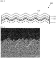
- FIG. 4 is a cross-sectional electron microscope image illustrating a substrate on which a texture having peak portions and valley portions is formed
- FIG. 5 is a cross-sectional electron microscope image illustrating a substrate on which a texture is formed, wherein the texture has peak and valley portions on which a rounding process is performed and thus have a round shape.
- the texture has peak and valley portions which are very sharp even in a microstructural sense, and the edges connecting a peak to a valley remain intact, maintaining a faceted structure.
- the texture has radii of curvature of about 15 to 20 nm before the rounding process.
- the edges are maintained at an angle of about 55 degrees relative to the surface of the substrate, assuming that the substrate is flat. This is attributed to the basic characteristics of a silicon (Si) substrate and of etching.
- Monocrystalline silicon substrates are generally classified into ⁇ 100 ⁇ plane substrates, ⁇ 111 ⁇ plane substrates, and the like according to a growth plane.
- silicon has a diamond cubic crystal structure and a face-centered cubic lattice structure.
- face-centered cubic lattice since a ⁇ 111 ⁇ plane is the most close-packed plane, the ⁇ 111 ⁇ planee is the most stable plane in terms of the binding energy of atoms.
- the faces to which the diagonal lines of the pyramidal structures constituting the texture belong are all ⁇ 111 ⁇ planes, and the angles made by the ⁇ 111 ⁇ planes relative to the horizontal direction of the substrate are about 55 degrees in the case of a cubic lattice.
- FIG. 5 illustrates a texture which has been rounded under isotropic etching conditions in the present disclosure.
- the substrate having a rounded texture as shown in FIG. 5 has several features unique to the present disclosure.
- the absolute values of the radii of curvature of the valley portions are greater than or equal to the absolute values of the radii of curvature of the peak portions.
- the peak portions which preferentially react with an etching component are preferentially etched over other portions.
- the radii of curvature of the peak portions become larger than the radii of curvature of valley portions, and when isotropic etching is continuously carried out for a sufficient period of time, the textured structure ultimately is removed due to the rapid etching of the peak portions. Therefore, only when the radii of curvature of valley portions are larger than the radii of curvature of peak portions as in the present disclosure, it is possible to uniformly form or convert a subsequent inter-layer and/or perovskite absorption layer as well as increasing the path of light by the textured structure of the substrate.
- the radii of curvature of the valley portions of the present disclosure are in a range of 0.05 to 50 ⁇ m.
- the radii of curvature are smaller than 0.05 ⁇ m, the rounding cannot bring about the effect of allowing a subsequent inter-layer and/or perovskite absorption layer to be uniformly formed.
- the radii of curvature exceed 50 ⁇ m, since the peak and valley portions are excessively etched away, the substrate is planarized. As a result, the texture cannot bring about its inherent effect of improving light absorption efficiency.
- the radii of curvature of the valley portions are measured to be approximately 0.07 to 1.2 ⁇ m.
- FIG. 5 clearly shows that the inclined surfaces connecting the valley portions to the peak portions in the texture form an angle of less than 55 degrees relative to the horizontal direction of the substrate.
- the inclined surfaces in FIG. 4 are ⁇ 111 ⁇ planes which are chemically the most stable in monocrystalline silicon.
- the above-described angle becomes less than 55 degrees which was measured before etching, as shown in FIG. 5 . This enables the uniform deposition of a inter-layer and/or a perovskite absorption layer even at the inclined surfaces.
- rounded textures having different contours from that of FIG. 5 may also be formed.
- FIG. 6 illustrates a texture according to another embodiment in which rounding has been accomplished by etching for about 10 minutes in an etching solution in which hydrofluoric acid and nitric acid are mixed in a ratio of 1:40.
- a thickness of a perovskite absorption layer formed at the valley portions and the peak portions differ by at most 10% in the present disclosure.
- the thickness of a perovskite absorption layer formed at the valley portions of the texture may differ from the thicknesses at the peak portions and the inclined surfaces of the texture by at most 10% in the present disclosure. Therefore, the present disclosure has the advantage that not only light efficiency is increased due to the texture, but also improved cell uniformity, which has only been attained in solar cells having flat interfaces, can be attained even in solar cells having textured interfaces.
- the inter-layer 114 is disposed on the emitter layer 112 of the first solar cell 110, thereby serving to bond the first solar cell 110 and the second solar cell 120 together. Accordingly, the second solar cell 120 is electrically connected to the first solar cell 110 through the inter-layer 114.
- the inter-layer 114 may be realized using a transparent conductive oxide (TCO), a carbonaceous conductive material, a metallic material, or a conductive polymer so that the light having a long wavelength transmitted through the second solar cell 120 can enter the first solar cell 110 disposed thereunder without transmission loss.
- TCO transparent conductive oxide
- the inter-layer 114 may be doped with an n-type or p-type material and used.
- indium tin oxide (ITO), zinc indium tin oxide (ZITO), zinc indium oxide (ZIO), zinc tin oxide (ZTO), gallium indium tin oxide (GITO), gallium indium oxide (GIO), gallium zinc oxide (GZO), aluminum-doped zinc oxide (AZO), fluorine tin oxide (FTO), ZnO, or the like may be used.
- carbonaceous conductive material graphene, carbon nanotubes, or the like may be used
- metallic material metal (Ag) nanowires or a metal thin film having a multilayer structure (e.g., Au/Ag/Cu/Mg/Mo/Ti) may be used.
- conductive polymer polyaniline, polypyrrole, polythiophene, PEDOT:PSS, PTAA, Spiro-MeOTAD, PANI-CSA, or the like may be used.
- the inter-layer 114 may also be realized as a multilayer structure in which silicon layers having different refractive indices are alternately stacked multiple times.
- the multilayer structure may include layers having a lower refractive index and layers having a higher refractive index, which are alternately stacked. Accordingly, with respect to the inter-layer 114, light having a short wavelength can be reflected toward the second solar cell 120, and light having a long wavelength can be transmitted toward the first solar cell 110. In this case, selective collection of light can be realized in the perovskite/silicon tandem solar cell.
- the second solar cell 120 of the present disclosure further includes an electron transport layer 121 and a hole transport layer 123 in addition to the perovskite absorption layer 122.
- the electron transport layer 121 may be disposed under the perovskite absorption layer 122, and the hole transport layer 123 may be disposed above the perovskite absorption layer 122.
- the positions of the electron transport layer 121 and the hole transport layer 123 may be switched as necessary.
- a metal oxide may be used for the electron transport layer 121.
- the metal oxides constituting the electron transport layer 121 include Ti oxide, Zn oxide, In oxide, Sn oxide, W oxide, Nb oxide, Mo oxide, Mg oxide, Zr oxide, Sr oxide, Yr oxide, La oxide, V oxide, Al oxide, Y oxide, Sc oxide, Sm oxide, Ga oxide, In oxide, SrTi oxide, and the like. More preferably, for the electron transport layer 121, at least one metal oxide selected from among ZnO, TiO 2 , SnO 2 , WO 3 , and TiSrO 3 is used.
- a mesoporous layer 125 including a metal oxide that is the same as or different from the metal oxide of the electron transport layer 121 may be further provided.
- the mesoporous layer 125 assists in facilitating the transfer of electrons or holes, particularly, electrons, to the inter-layer 114 to be described below after hole-electron pairs generated in the perovskite absorption layer 122 are broken into holes and electrons.
- the mesoporous layer 125 also serves to lengthen the path of light by forming a light-scattering structure.
- the perovskite absorption layer 122 is a photoactive layer including a compound having a perovskite structure, wherein the perovskite structure may be represented as AMX 3 (here, A refers to a monovalent organic ammonium cation or metal cation; M refers to a divalent metal cation; and X refers to a halogen anion).
- AMX 3 here, A refers to a monovalent organic ammonium cation or metal cation
- M refers to a divalent metal cation
- X refers to a halogen anion
- Non-limiting examples of compounds having a perovskite structure include CH 3 NH 3 PbI 3 , CH 3 NH 3 PbI x Cl 3-x , CH 3 NH 3 PbI x Br 3-x , CH 3 NH 3 PbCl x Br 3-x , HC(NH 2 ) 2 PbI 3 , HC(NH 2 ) 2 PbI x Cl 3-x , HC(NH 2 ) 2 PbI x Br 3-x , HC(NH 2 ) 2 PbCl x Br 3-x , (CH 3 NH 3 )(HC(NH 2 ) 2 ) 1-y PbI 3 , (CH 3 NH 3 )(HC(NH 2 ) 2 ) 1-y PbI x Cl 3-x , (CH 3 NH 3 )(HC(NH 2 ) 2 ) 1-y PbI x Br 3-x , (CH 3 NH 3 )(HC(NH 2 ) 2 ) 1-y PbI x Br
- the hole transport layer 123 may be realized using a conductive polymer. That is, as the conductive polymer, polyaniline, polypyrrole, polythiophene, poly(3,4-ethylenedioxythiophene)-poly(styrenesulfonate) (PEDOT:PSS), poly[bis(4-phenyl)(2,4,6-trimethylphenyl)amine] (PTAA), Spiro-MeOTAD, polyaniline-camphorsulfonic acid (PANI-CSA), or the like may be used. In this case, the hole transport layer 123 may further include an n-type or p-type dopant as necessary.
- a conductive polymer polyaniline, polypyrrole, polythiophene, poly(3,4-ethylenedioxythiophene)-poly(styrenesulfonate) (PEDOT:PSS), poly[bis(4-phenyl)(2,4,6-trimethylphenyl)amine] (PTAA), Spiro
- the second electrode 130 is disposed on the second solar cell 120.
- the second electrode 130 may be directly disposed, in the form of a grid, on the second solar cell 120. That is, the second electrode 130 may be formed of only a grid electrode layer 118 directly disposed on the second solar cell 120, without including a transparent electrode layer 116.
- the second electrode 130 may include a transparent electrode layer 116 disposed on the second solar cell 120 and a grid electrode layer 118 disposed on the transparent electrode layer 116.
- the transparent electrode layer 116 is formed on the entire upper surface of the second solar cell 120, thereby serving to collect electrical charges generated in the second solar cell 120.
- Such a transparent electrode layer 116 may be realized using various transparent conductive materials. That is, as the transparent conductive material, the same material as the transparent conductive material of the inter-layer 114 may be used.
- the grid electrode layer 118 is disposed on the transparent electrode layer 116, and is disposed on some parts of the transparent electrode layer 116.
- a buffer layer may be further disposed, but the addition thereof is not always required, and the buffer layer may be omitted as necessary.
- a transparent conductive compound or the like is preferable for the buffer layer. More specifically, as the transparent conductive oxide, ITO, ZITO, ZIO, ZTO, GITO, GIO, GZO, AZO, FTO, ZnO, or the like may be used.
- the first electrode 140 is disposed on the first surface of the crystalline silicon substrate 111.
- the first electrode 140 may be directly disposed, in the form of a grid, at the rear of the first solar cell 110. That is, the first electrode 140 may be formed of only a grid electrode layer 119 directly provided at the rear of the first solar cell 110, without including a transparent electrode layer 117.
- the first electrode 140 may include a transparent electrode layer 117 disposed at the rear of the first solar cell 110 and a grid electrode layer 119 disposed on the transparent electrode layer 117.
- Such a first electrode 140 is electrically connected to the BSF layer 113.
- the first electrode 140 is designed such that it is not disposed on the entire rear surface of the BSF layer 113 but only on some parts of the rear surface of the BSF layer 113 to allow sunlight to enter through the rear surface of the first solar cell 110.
- the first electrode 140 is preferably disposed such that it occupies 1 to 30% of the total rear surface area of the BSF layer 113.
- the first electrode 140 occupies less than 1% of the area, there is a concern that the effect of the first electrode 140 collecting electrical charges generated in the first solar cell 110 may be insufficient. On the other hand, when the first electrode 140 occupies more than 30% of the area, since an excessively large area is occupied by the first electrode 140, there is a concern that the utilization rate of the light entering through the rear surface of the first solar cell 110 may be lowered.
- the first electrode 140 and the second electrode 130 of the present disclosure may be simultaneously formed. This is because, when a hydrogenated intrinsic amorphous silicon (i a-Si:H) layer is used as the passivation layer, the process temperature is limited to 250 °C or less to prevent the breaking of hydrogen bonds in the amorphous silicon. In this case, the first electrode 140 and the second electrode 130 may be formed through low-temperature firing at 250 °C or less using a first electrode paste that does not contain glass frit.
- a hydrogenated intrinsic amorphous silicon (i a-Si:H) layer is used as the passivation layer
- the process temperature is limited to 250 °C or less to prevent the breaking of hydrogen bonds in the amorphous silicon.
- the first electrode 140 and the second electrode 130 may be formed through low-temperature firing at 250 °C or less using a first electrode paste that does not contain glass frit.
- the first electrode 140 and the second electrode 130 may be formed using two processes and not simultaneously, such that a higher-temperature firing process is carried out at 700 °C or more to form the first electrode 140 and a lower-temperature firing process is carried out at 250 °C or less using a second electrode paste not containing glass frit to form the second electrode 130.
- the second solar cell 120 and then the second electrode 130 after first forming the first electrode 140 by the high-temperature firing process.
- the second solar cell 120 is exposed only to the firing process for forming the second electrode 130 which is carried out at a lower temperature of 250 °C or less, since there is no concern that the second solar cell 120 is exposed to the firing process for forming the first electrode 140 which is carried out at a higher temperature of 700 °C or more, the problem that the second solar cell 120 is degraded by high-temperature firing can be prevented in advance.
- FIGS. 7 to 13 are cross-sectional views illustrating the processes of a method of manufacturing a tandem solar cell according to one embodiment of the present disclosure.
- a texturing pattern is formed by planarizing the first and second surfaces of a crystalline silicon substrate 111 and then texturizing at least one of the first and second surfaces.
- the textured structure may be introduced to the crystalline silicon substrate 111 using any one method among a wet chemical etching method, a dry chemical etching method, an electrochemical etching method, and a mechanical etching method, but the present disclosure is not limited thereto.
- the textured structure may be introduced by etching at least one of the first and second surfaces of the crystalline silicon substrate 111 in a basic aqueous solution.
- an n-type monocrystalline silicon substrate that has a thickness of several hundreds of micrometers to several thousands of micrometers and has been sliced along a (100) plane is provided.
- a surface of the substrate is etched at a temperature ranging from room temperature to 150 °C using an aqueous solution prepared by adding an additive(s) such as an organic solvent, a phosphate, a reaction regulator and/or a surfactant to a 1 to 5 wt% aqueous sodium hydroxide (NaOH) solution or aqueous potassium hydroxide (KOH) solution.
- an additive(s) such as an organic solvent, a phosphate, a reaction regulator and/or a surfactant to a 1 to 5 wt% aqueous sodium hydroxide (NaOH) solution or aqueous potassium hydroxide (KOH) solution.
- the organic solvent may be at least any one of 2-methyl-2,4-pentanediol, propylene glycol, 2,2,4-trimethyl-1,3-pentanediol, 1,3-butanediol, 1,4-butanediol, 1,6-hexanediol, 2,2-dimethyl-1,3-propanediol, hydroquinone, 1,4-cyclohexanediol, and N-methyl prolyl.
- the phosphate may be at least any one of K 3 PO 4 and K 2 HPO 4 .
- a texture having pyramidal irregularities is formed on a monocrystalline silicon substrate. Since monocrystalline silicon has a diamond cubic structure, a ⁇ 111 ⁇ plane is the most close-packed and chemically stable plane. Therefore, since etching in a sodium hydroxide solution is therefore the slowest in the ⁇ 111 ⁇ plane, after etching, anisotropic etching is found along the ⁇ 111 ⁇ plane of the silicon substrate. As a result, a texture having a depth of about 0.1 to 10 ⁇ m is uniformly formed on an entire surface of the silicon substrate.
- the texture is etched to form a rounded texture as shown in FIG. 7B .
- the rounding process may be carried out by any one of wet etching, sputtering etching, reactive ion etching, and vapor-phase etching.
- wet etching of silicon substrates HNO 3 /HF, KOH, tetramethylammonium hydroxide (TMAH), or other similar chemicals are used.
- TMAH tetramethylammonium hydroxide
- dry etching which may be exemplified by reactive ion etching, uses a chemically reactive plasma in order to remove a material deposited on a surface. Dry etching has advantages in that it can be applied to all types of silicon surfaces regardless of the crystallinity of the silicon substrates, does not require a mask, and consumes less gas compared to the amount of chemicals consumed in wet etching. However, due to including several steps, dry etching has a disadvantage in that the process thereof is somewhat complex and requires several types of working gases.
- any etching process can be applied as long as it allows for isotropic etching not anisotropic etching.
- the textured substrate was subjected to the rounding process using an etching solution in which hydrofluoric acid and nitric acid are mixed in a ratio of 1:(10 to 80), wherein the rounding process was carried out at a temperature not exceeding room temperature while adjusting the etching time.
- etching solution in which hydrofluoric acid and nitric acid are mixed in a ratio of 1:(10 to 80)
- the rounding process was carried out at a temperature not exceeding room temperature while adjusting the etching time.
- the proportion of hydrofluoric acid is increased and thus the ratio becomes greater than 1:10, that is, when the proportion of nitric acid is decreased, since etching becomes excessively slow, the effect of rounding cannot be easily exhibited.
- pre-treatment of the textured substrate may be carried out before the rounding process.
- the substrate in order to remove an oxide film from a surface of the substrate, the substrate may be immersed in an aqueous solution in which hydrofluoric acid and pure water are mixed in an arbitrary ratio.
- processes of oxidizing the surface using hydrochloric acid (HCl) and/or an aqueous solution containing hydrogen peroxide (H 2 O 2 ) and then removing the oxidized film may be further carried out.
- an emitter layer 112 is formed on the second surface of the crystalline silicon substrate 111.
- a back surface field layer 113 may be further formed on the first surface of the crystalline silicon substrate 111 (see FIG. 8 ).
- an amorphous intrinsic silicon (i a-Si:H) layer as a passivation layer is first deposited, by a plasma-enhanced chemical vapor deposition (PECVD) method using a silicon source material (SiH 4 , Si 2 H 6 , etc.) and hydrogen (H 2 ), on a uniformly textured n-type silicon crystalline substrate.
- PECVD plasma-enhanced chemical vapor deposition
- SiH 4 silicon source material
- Si 2 H 6 Si 2 H 6
- H 2 hydrogen
- the PECVD method is particularly preferred as a method of manufacturing a heterojunction silicon solar cell because of the advantage that a process temperature can be lowered compared to common chemical vapor deposition (CVD) methods.
- a back surface field layer 113 doped with impurities of the same conductivity type as that of the silicon crystalline substrate are formed.
- a PECVD process is used, and one or more types of gases selected from the group consisting of SiH 4 , Si 2 H 6 , SiHCl 3 , and SiH 2 Cl 2 and H 2 gas are used as reactants, and B 2 B 6 or PH 3 gas is used as a dopant gas.
- the temperature and pressure conditions of the PECVD process may be the same as the PECVD conditions for the amorphous intrinsic silicon layer.
- the first solar cell 110 When the first solar cell 110 is a heterojunction silicon solar cell, the first solar cell 110 can have a structure in which very thin amorphous intrinsic silicon (i a-Si:H) as a passivation layers are first formed on front and rear sides of an n-type crystalline silicon substrate, a p-type high-concentration amorphous silicon (p a-Si:H) layer as an emitter layer 112 is formed on the front side, and a high-concentration amorphous silicon (n+ a-Si:H) layer as a back surface field (hereinafter abbreviated as BSF) layer 113 is formed on the rear side.
- amorphous intrinsic silicon i a-Si:H
- p a-Si:H p-type high-concentration amorphous silicon
- n+ a-Si:H high-concentration amorphous silicon
- BSF back surface field
- an emitter layer 112 and a BSF layer 113 may be formed through an ion implantation process.
- the emitter layer 112 is doped with boron as an impurity
- the BSF layer 113 is doped with phosphorous as an impurity.
- heat treatment is also performed at 700 to 1,200 °C to activate the impurities.
- the emitter layer 112 and the BSF layer 113 may also be formed through a high-temperature diffusion process using BBr 3 , POCl 3 , or the like, instead of the ion implantation process.
- the first electrode 140 is formed on the first surface of the crystalline silicon substrate 111.
- the process temperature for the first electrode 140 as well as the process temperature for the second electrode 130 is limited to 250 °C or less.
- the first electrode 140 may be formed before the second electrode 130 is formed, or the first electrode 140 and the second electrode 130 may be simultaneously formed.
- a transparent electrode layer 117 is first formed on the BSF layer 113.
- a transparent conductive oxide such as ITO, ZITO, ZIO, ZTO, or the like is used as a material for the transparent electrode layer
- the transparent electrode layer 117 may be deposited by sputtering.
- a grid electrode layer 119 is formed.
- the grid electrode layer 119 it is also possible to form the grid electrode layer 119 directly on the BSF layer 113 without forming the transparent electrode layer 117, since the carrier mobility of amorphous silicon is rather low to collect carriers through a metal grid, it is more preferred that a transparent electrode layer 117 is formed.
- the grid electrode layer 119 is formed by applying a second electrode paste on the transparent electrode layer 117 by a screen-printing method and carrying out heat treatment at a first temperature (which is the same as a second temperature).
- the first electrode 140 may be formed by selectively applying a first electrode paste not containing glass frit and then carrying out low-temperature firing at a first temperature.
- the first electrode paste may contain metal particles and an organic material which is a binder for low-temperature firing, and the first electrode paste does not contain glass frit.
- the first temperature may be 250 °C or less and more specifically in a range of 100 to 200 °C.
- the first electrode 140 and the second electrode 130 may be formed using two processes and not simultaneously such that a higher-temperature firing process is carried out at 700 °C or more to form the first electrode 140 and a lower-temperature firing process is carried out at 250 °C or less using a second electrode paste not containing glass frit to form the second electrode 130.
- the second electrode paste may be any one selected from among an Ag paste and an Ag/Al paste.
- the first electrode paste contains glass frit and an inorganic additive such as Ag particles, Ag/Al particles, or the like, and the first temperature may be 700 °C or more and more specifically in a range of 700 to 1,100 °C.
- the first electrode 140 is preferably designed such that it is not disposed on an entire rear surface of the BSF layer 113 but only on some parts of the rear surface of the BSF layer 113 to allow sunlight to enter through the rear surface of the first solar cell 110.
- the first electrode 140 is preferably disposed such that it occupies 1 to 30% of the total rear surface area of the BSF layer 113.
- a inter-layer 114 is formed on the emitter layer 112.
- the inter-layer 114 As a material for the inter-layer 114, a transparent conductive oxide, a carbonaceous conductive material, a metallic material, or a conductive polymer may be used.
- the inter-layer may be doped with an n-type or p-type material and used.
- the inter-layer 114 may be deposited by sputtering.
- an n-type amorphous silicon layer may be deposited by PECVD to form the inter-layer 114.
- the textured substrate of the present disclosure having rounded valley and peak portions enables the uniform deposition of a inter-layer 114 particularly at peak portions when the deposition is carried out through a thin-film deposition process.
- the radii of curvature of the peak portions i.e., the sharper the peak portions become
- the thickness of the inter-layer 114 formed on a texture becomes smaller at peak portions than at other portions.
- the inter-layer 114 is formed such that it has a uniform thickness at peak portions and other portions. It can be seen that this result directly proves the effect of rounding a texture in the present disclosure.
- a second solar cell 120 is formed on the inter-layer 114.
- an operation of forming the second solar cell includes an operation of forming an electron transport layer 121 on the inter-layer 114, an operation of forming a perovskite absorption layer 122 on the electron transport layer 121, and an operation of forming a hole transport layer 123 on the perovskite absorption layer 122.
- an operation of forming a mesoporous layer may be further included between the operation of forming an electron transport layer and the operation of forming a perovskite absorption layer.
- the electron transport layer 121 and the mesoporous layer 125 may be formed of the same metal oxide.
- the electron transport layer 121 may be formed as a TiO 2 layer having a thickness of 5 to 100 nm
- the mesoporous layer 125 may be formed as a TiO 2 layer having a thickness of 500 nm or less.
- perovskite absorption layers are mainly formed through a so-called solution process such as inkjet printing, gravure printing, spray coating, doctor-blade coating, bar coating, gravure coating, brush painting, slot-die coating, or the like.
- solution processes have advantages in that a light absorption constituting a photoactivation layer can be formed through very simple, easy, and inexpensive processes of applying and drying a solution.
- the solution processes also have the advantage that a light absorption having coarse crystal grains can be formed, and, particularly, excellent conductivity for both electrons and holes is attained because spontaneous crystallization occurs due to the drying of an applied solution.
- solution process in a solution process, following the application of a solution to a substrate having a textured structure consisting of irregularities as in the present disclosure, the film is planarized due to leveling characteristics thereof. In this case, since the path of the light transmitted through the second electrode 130 is shortened and reflectance is increased, there is a high possibility that solar cell efficiency may be lowered.
- an electron transport layer or a mesoporous layer is first formed on the substrate having a rounded texture, and then a perovskite absorption layer that conforms to the textured surface is formed on the electron transport layer or mesoporous layer.
- the perovskite absorption layer is formed by physical vapor deposition using sputtering or an electron beam or by chemical vapor deposition.
- the perovskite absorption layer may be formed by any one of single-step deposition and sequential-step deposition, since it is difficult to form a uniform thin film by the single-step deposition, the sequential-step deposition is more preferred.
- the deposition of the first precursor layer is accomplished by forming a first precursor layer made of PbI 2 on the textured electron transport layer 121 or mesoporous layer 125 by sputtering.
- the deposition of the first precursor layer is carried out under inert gas (Ar, He, or Ne) pressure conditions of 0.1 to 20 mTorr and electric power conditions of 100 to 300 W, using a target containing a PbI 2 component.
- inert gas Ar, He, or Ne
- the temperature of a substrate is maintained within a range of room temperature to 100 °C.
- RF sputtering which uses radio frequency is used as the sputtering method.
- a second precursor layer having a CH 3 NH 3 I composition is formed on the PbI 2 layer.
- the second precursor layer may also be formed of components which have an AX structure, wherein A includes one or more among a monovalent C 1 -C 20 alkyl group, an alkyl group substituted with an amine group, and an alkali metal, and X includes one or more among F - , Cl - , Br - , and I - .
- processes such as a thermal evaporation method, sputtering, a CVD method, a spin coating method, a dip coating method, a spraying method, and the like may be used, and unlike in the formation of the first precursor layer, there is no particular limitation.
- a post-thermal process is carried out to form a thin perovskite layer.
- the post-thermal process is carried out at a temperature ranging from room temperature to 200 °C for at most about three hours.
- a lower limit of the post-thermal temperature is not particularly limited, and at a temperature exceeding 200 °C, the second precursor layer may undergo thermal decomposition or a change in composition caused by thermal decomposition before even reacting with the first precursor layer to form a perovskite layer.
- the components of the second precursor layer penetrate into the first precursor layer which is a porous layer, to form a perovskite photoactive layer.
- a final thickness of the perovskite absorption layer obtained by such a process becomes substantially the same as the thickness of the first precursor layer. This is because the final perovskite layer is formed by the penetration of the components of the second precursor layer into the porous first precursor layer.
- the textured substrate of the present disclosure having rounded valley and peak portions has a synergistic effect in combination with the above-described method of forming a porous precursor layer.
- a porous precursor layer for a perovskite absorption layer before materials which have been deposited reach a stable and dense deposition position, it is required that other subsequent materials being deposited from a deposition source onto a substrate reach the substrate. In other words, the deposition should be maintained at a relatively high speed in a general sense. Under such a deposition mechanism, there is a problem that it is difficult for a material to be deposited to reach and be deposited on a texture including valleys having a radius of curvature of several nanometers to several tens of nanometers.
- a porous precursor layer can be uniformly deposited throughout the texture, including the valley portions, even at a high deposition rate. For this reason, the present disclosure has a very advantageous effect in achieving tandem solar cell uniformity.
- the hole transport layer 123 is a layer which allows the holes generated in the perovskite layer to be easily transferred to the second electrode 130, and should be able to ensure the ability to transmit visible light and conduct holes.
- a polymer material is generally suitable as a material for the hole transport layer 123.
- a hole transport layer may be formed by carrying out spin coating for 40 to 50 seconds at a speed of 3000 to 5000 rpm using a polymer material such as PEDOT:PSS.
- a solution process such as a printing process may be applied after dissolving any one of PEDOT:PSS, poly(9-vinylcarbazole) (PVK), poly[(9,9-dioctylfluorenyl-2,7-diyl)-co-(4,4'(N-(4-sec-butylphenyl)diphenylamine))] (TFB), copper phthalocyanine (CuPc), N,N'-diphenyl-N,N'-bis(1-naphthyl)-1,1'-biphenyl-4,4'-diamine (a-NPD), and N,N'-bis-(3-methylphenyl)-N,N'-bis-phenyl(1,1'-biphenyl)-4,4'-diamine (TPD) into a liquid phase.
- PEDOT:PSS poly(9-vinylcarbazole)
- PVK poly[(9,9-d
- the hole transport layer 123 may include a monomer or polymer hole transport material or a metal oxide besides the above-described components.
- a solution process such as a dip coating method, a spraying method, or the like or even a deposition process such as a thermal evaporation method, a sputtering method, or the like may also be applied.
- a buffer layer 115 may be formed as necessary. It is basically required that the buffer layer has the ability to transmit visible light while being able to protect the perovskite layer thereunder.
- a transparent conductive compound or the like is preferable for the buffer layer 115. More specifically, as the transparent conductive oxide, ITO, ZITO, ZIO, ZTO, GITO, GIO, GZO, AZO, FTO, ZnO, or the like may be used.
- a second electrode 130 is formed on the buffer layer 115 or the hole transport layer 123.
- the second electrode 130 may include a transparent electrode layer 116 disposed on the second solar cell 120 and a grid electrode layer 118 disposed on the transparent electrode layer 116 (see FIG. 13 ).
- the transparent electrode layer 116 is formed on the entire upper surface of the second solar cell 120, thereby serving to collect electrical charges generated in the second solar cell 120.
- Such a transparent electrode layer 116 may be realized using various transparent conductive materials. That is, as the transparent conductive material, the same material as the transparent conductive material of the inter-layer 114 may be used.
- the grid electrode layer 118 is disposed on the transparent electrode layer 116, and is disposed on some parts of the transparent electrode layer 116.
- the second electrode 130 may be formed by selectively applying a second electrode paste not containing glass frit and then carrying out low-temperature firing at a second temperature.
- a second electrode paste may contain metal particles and an organic material which is a binder for low-temperature firing, and the second electrode paste does not contain glass frit.
- the second temperature may be 250 °C or less and more specifically in a range of 100 to 200 °C.
- the first electrode 140 may be simultaneously formed with the second electrode 130 during the formation of the second electrode 130, or the second electrode 130 may be formed after the first electrode 140 and then the second solar cell are formed.
- both the first electrode 140 and the second electrode 130 are formed by a firing process carried out at a lower temperature of 250 °C or less.
- first and second electrodes should be formed separately through a firing process which is carried out at a higher temperature of 700 °C or more and in which the first electrode 140 is formed and a firing process which follows the formation of a second solar cell 120 and is carried out at a lower temperature of 250 °C or less and in which the second electrode 130 is formed. This is to prevent in advance the problem that the second solar cell 120 is degraded by high-temperature firing.
- a tandem solar cell of the present disclosure since it is possible to improve cell reliability by securing uniformity in the deposition and conversion of a perovskite film and preventing short circuits, reduce the reflectance of light, and increase the path of light at the same time, cell characteristics can be improved.
- the texture is rounded by isotropic etching, and a inter-layer and a porous perovskite precursor layer are formed on the texture.
- the method of manufacturing a tandem solar cell according to one embodiment of the present disclosure enables the formation of a conformal inter-layer and a conformal perovskite absorption layer that have a uniform thickness while thoroughly mirroring the contour of a substrate having a textured structure that has been rounded.
Landscapes
- Engineering & Computer Science (AREA)
- Chemical & Material Sciences (AREA)
- Materials Engineering (AREA)
- Chemical Kinetics & Catalysis (AREA)
- Electrochemistry (AREA)
- Power Engineering (AREA)
- Microelectronics & Electronic Packaging (AREA)
- Physics & Mathematics (AREA)
- Electromagnetism (AREA)
- Photovoltaic Devices (AREA)
- Life Sciences & Earth Sciences (AREA)
- Sustainable Development (AREA)
- Sustainable Energy (AREA)
- Manufacturing & Machinery (AREA)
Priority Applications (1)
| Application Number | Priority Date | Filing Date | Title |
|---|---|---|---|
| EP25182401.7A EP4629809A3 (de) | 2017-05-29 | 2018-05-28 | Perowskit-silicium-tandemsolarzelle und herstellungsverfahren dafür |
Applications Claiming Priority (2)
| Application Number | Priority Date | Filing Date | Title |
|---|---|---|---|
| KR1020170066437A KR102541379B1 (ko) | 2017-05-29 | 2017-05-29 | 페로브스카이트 실리콘 탠덤 태양전지 및 제조 방법 |
| PCT/KR2018/006048 WO2018221914A1 (ko) | 2017-05-29 | 2018-05-28 | 페로브스카이트 실리콘 탠덤 태양전지 및 제조 방법 |
Related Child Applications (1)
| Application Number | Title | Priority Date | Filing Date |
|---|---|---|---|
| EP25182401.7A Division EP4629809A3 (de) | 2017-05-29 | 2018-05-28 | Perowskit-silicium-tandemsolarzelle und herstellungsverfahren dafür |
Publications (4)
| Publication Number | Publication Date |
|---|---|
| EP3633736A1 true EP3633736A1 (de) | 2020-04-08 |
| EP3633736A4 EP3633736A4 (de) | 2021-03-17 |
| EP3633736C0 EP3633736C0 (de) | 2025-07-02 |
| EP3633736B1 EP3633736B1 (de) | 2025-07-02 |
Family
ID=64456002
Family Applications (2)
| Application Number | Title | Priority Date | Filing Date |
|---|---|---|---|
| EP25182401.7A Pending EP4629809A3 (de) | 2017-05-29 | 2018-05-28 | Perowskit-silicium-tandemsolarzelle und herstellungsverfahren dafür |
| EP18810525.8A Active EP3633736B1 (de) | 2017-05-29 | 2018-05-28 | Perowskit-silizium-tandemsolarzelle und herstellungsverfahren |
Family Applications Before (1)
| Application Number | Title | Priority Date | Filing Date |
|---|---|---|---|
| EP25182401.7A Pending EP4629809A3 (de) | 2017-05-29 | 2018-05-28 | Perowskit-silicium-tandemsolarzelle und herstellungsverfahren dafür |
Country Status (5)
| Country | Link |
|---|---|
| US (1) | US20210126147A1 (de) |
| EP (2) | EP4629809A3 (de) |
| KR (1) | KR102541379B1 (de) |
| PL (1) | PL3633736T3 (de) |
| WO (1) | WO2018221914A1 (de) |
Cited By (3)
| Publication number | Priority date | Publication date | Assignee | Title |
|---|---|---|---|---|
| WO2023156123A1 (de) * | 2022-02-18 | 2023-08-24 | Singulus Technologies Ag | Erzeugung texturierter oberflächen, herstellung von tandemsolarzellen und tandemsolarzelle |
| EP4503142A1 (de) * | 2023-07-31 | 2025-02-05 | Jinko Solar Co., Ltd | Tandemzelle, verfahren zur herstellung davon und fotovoltaisches modul |
| WO2025080463A1 (en) * | 2023-10-13 | 2025-04-17 | Northrop Grumman Systems Corporation | Light trapping device for thin film space photovoltaics |
Families Citing this family (16)
| Publication number | Priority date | Publication date | Assignee | Title |
|---|---|---|---|---|
| KR102584087B1 (ko) * | 2018-03-19 | 2023-10-04 | 상라오 징코 솔라 테크놀러지 디벨롭먼트 컴퍼니, 리미티드 | 텐덤 태양전지의 제조 방법 |
| WO2021030491A1 (en) | 2019-08-12 | 2021-02-18 | Arizona Board Of Regents On Behalf Of Arizona State University | Perovskite/silicon tandem photovoltaic device |
| CN111261779B (zh) * | 2020-02-14 | 2025-06-10 | 常熟理工学院 | 一种硅基叠层太阳能电池及其制备方法 |
| CN111952377A (zh) * | 2020-08-24 | 2020-11-17 | 中国科学院半导体研究所 | 曲面陷光结构的钙钛矿/硅叠层太阳电池及其制作方法 |
| CN112133830A (zh) * | 2020-09-11 | 2020-12-25 | 上海黎元新能源科技有限公司 | 一种2-t钙钛矿叠层太阳能电池模块及其制备方法 |
| KR102792265B1 (ko) * | 2021-04-12 | 2025-04-09 | 주성엔지니어링(주) | 태양 전지 및 그 제조 방법 |
| FR3125185A1 (fr) | 2021-07-09 | 2023-01-13 | Electricite De France | Procede d’optimisation de la duree de vie d’un module photovoltaique bifacial multijonctions et module ou panneau photovoltaique adapte a ce procede |
| CN115768145A (zh) * | 2021-09-01 | 2023-03-07 | 隆基绿能科技股份有限公司 | 一种叠层太阳能电池及光伏组件 |
| CN115763607B (zh) * | 2021-09-01 | 2024-10-29 | 隆基绿能科技股份有限公司 | 彩色叠层光伏器件 |
| CN116133448B (zh) * | 2021-11-12 | 2026-01-09 | 西安隆基乐叶光伏科技有限公司 | 一种钙钛矿-硅基叠层太阳能电池及其制作方法 |
| KR102688198B1 (ko) * | 2022-06-22 | 2024-07-24 | 성균관대학교산학협력단 | 탠덤 태양전지 셀, 탠덤 태양전지 모듈 및 이의 제조 방법 |
| CN115377234A (zh) * | 2022-07-21 | 2022-11-22 | 中国科学院宁波材料技术与工程研究所 | 一种钙钛矿晶体硅叠层太阳电池及其制备方法 |
| KR102818793B1 (ko) | 2023-02-08 | 2025-06-10 | 성균관대학교산학협력단 | 페로브스카이트 태양전지 및 그 제조방법 |
| JP3254369U (ja) * | 2023-12-27 | 2026-01-19 | 深▲セン▼市華宝新能源股▲フン▼有限公司 | 曲面型太陽光発電モジュール及び太陽光発電建築面 |
| KR102838135B1 (ko) * | 2024-02-15 | 2025-07-24 | 충남대학교산학협력단 | 실리콘 페로브스카이트 탠덤 소자 제조 방법 |
| CN121240747A (zh) * | 2025-12-03 | 2025-12-30 | 晶科能源(海宁)有限公司 | 叠层电池的制备方法、叠层电池和光伏组件 |
Family Cites Families (12)
| Publication number | Priority date | Publication date | Assignee | Title |
|---|---|---|---|---|
| JP3271990B2 (ja) * | 1997-03-21 | 2002-04-08 | 三洋電機株式会社 | 光起電力素子及びその製造方法 |
| JP2009064981A (ja) * | 2007-09-06 | 2009-03-26 | Toppan Printing Co Ltd | 太陽電池モジュールおよび透光性部材の製造方法 |
| US8247312B2 (en) * | 2008-04-24 | 2012-08-21 | Innovalight, Inc. | Methods for printing an ink on a textured wafer surface |
| FR2955707B1 (fr) | 2010-01-27 | 2012-03-23 | Commissariat Energie Atomique | Procede de realisation d'une cellule photovoltaique avec preparation de surface d'un substrat en silicium cristallin |
| KR102049604B1 (ko) * | 2011-12-16 | 2019-11-28 | 주성엔지니어링(주) | 태양전지 및 그 제조 방법 |
| JP6308438B2 (ja) * | 2012-10-23 | 2018-04-11 | パナソニックIpマネジメント株式会社 | 太陽電池 |
| JP6277555B2 (ja) | 2012-11-29 | 2018-02-14 | パナソニックIpマネジメント株式会社 | 太陽電池 |
| KR101382631B1 (ko) * | 2013-04-11 | 2014-04-14 | (주)울텍 | 태양전지기판의 표면 조직화 구조 형성 방법 및 이를 이용하여 제작된 태양전지기판 |
| CN107078179B (zh) | 2014-09-30 | 2019-04-26 | 株式会社钟化 | 晶体硅太阳能电池的制造方法、及太阳能电池模块的制造方法 |
| GB201510351D0 (en) * | 2015-06-12 | 2015-07-29 | Oxford Photovoltaics Ltd | Method of depositioning a perovskite material |
| US9608159B2 (en) | 2016-05-09 | 2017-03-28 | Solar-Tectic Llc | Method of making a tandem solar cell having a germanium perovskite/germanium thin-film |
| CN106252513A (zh) * | 2016-08-02 | 2016-12-21 | 天津工业大学 | 基于绒面光管理结构的钙钛矿太阳电池及其制备方法 |
-
2017
- 2017-05-29 KR KR1020170066437A patent/KR102541379B1/ko active Active
-
2018
- 2018-05-28 US US16/617,917 patent/US20210126147A1/en not_active Abandoned
- 2018-05-28 PL PL18810525.8T patent/PL3633736T3/pl unknown
- 2018-05-28 EP EP25182401.7A patent/EP4629809A3/de active Pending
- 2018-05-28 WO PCT/KR2018/006048 patent/WO2018221914A1/ko not_active Ceased
- 2018-05-28 EP EP18810525.8A patent/EP3633736B1/de active Active
Cited By (4)
| Publication number | Priority date | Publication date | Assignee | Title |
|---|---|---|---|---|
| WO2023156123A1 (de) * | 2022-02-18 | 2023-08-24 | Singulus Technologies Ag | Erzeugung texturierter oberflächen, herstellung von tandemsolarzellen und tandemsolarzelle |
| EP4503142A1 (de) * | 2023-07-31 | 2025-02-05 | Jinko Solar Co., Ltd | Tandemzelle, verfahren zur herstellung davon und fotovoltaisches modul |
| US12446389B2 (en) | 2023-07-31 | 2025-10-14 | Zhejiang Jinko Solar Co., Ltd. | Tandem cell, method for preparing the same, and photovoltaic module |
| WO2025080463A1 (en) * | 2023-10-13 | 2025-04-17 | Northrop Grumman Systems Corporation | Light trapping device for thin film space photovoltaics |
Also Published As
| Publication number | Publication date |
|---|---|
| KR102541379B1 (ko) | 2023-06-08 |
| EP3633736C0 (de) | 2025-07-02 |
| EP3633736B1 (de) | 2025-07-02 |
| US20210126147A1 (en) | 2021-04-29 |
| KR20180130396A (ko) | 2018-12-07 |
| EP3633736A4 (de) | 2021-03-17 |
| WO2018221914A1 (ko) | 2018-12-06 |
| EP4629809A3 (de) | 2025-11-12 |
| EP4629809A2 (de) | 2025-10-08 |
| PL3633736T3 (pl) | 2025-11-24 |
Similar Documents
| Publication | Publication Date | Title |
|---|---|---|
| EP3633736B1 (de) | Perowskit-silizium-tandemsolarzelle und herstellungsverfahren | |
| EP3637478B1 (de) | Verfahren zur herstellung einer perowskit-silicium-tandemsolarzelle | |
| KR102570856B1 (ko) | 페로브스카이트 태양전지 및 이를 포함하는 탬덤 태양전지 | |
| KR102756417B1 (ko) | 텐덤 태양전지 | |
| JP6524150B2 (ja) | タンデム太陽電池、これを含むタンデム太陽電池モジュール及びこの製造方法 | |
| EP3712967B1 (de) | Verfahren zur herstellung einer solarzelle | |
| KR102367784B1 (ko) | 텐덤 태양전지, 이를 포함하는 텐덤 태양전지 모듈 및 이의 제조방법 | |
| KR102564282B1 (ko) | 텐덤 태양전지 및 이의 제조방법 | |
| KR102531881B1 (ko) | 탠덤 태양전지 | |
| KR102474480B1 (ko) | 태양전지의 제조 방법 | |
| KR20180018895A (ko) | 양면 수광형 실리콘 태양전지 | |
| KR20180063866A (ko) | 텐덤 태양전지 및 그 제조 방법 | |
| US11515443B2 (en) | Tandem solar cell manufacturing method | |
| CN118053922A (zh) | 太阳能电池及其制备方法、光伏组件 | |
| JP2014192370A (ja) | 結晶シリコン太陽電池、およびその製造方法、ならびに太陽電池モジュール | |
| EP4404280A1 (de) | Solarzelle | |
| KR20120070315A (ko) | 태양 전지 및 그 제조 방법 |
Legal Events
| Date | Code | Title | Description |
|---|---|---|---|
| STAA | Information on the status of an ep patent application or granted ep patent |
Free format text: STATUS: THE INTERNATIONAL PUBLICATION HAS BEEN MADE |
|
| PUAI | Public reference made under article 153(3) epc to a published international application that has entered the european phase |
Free format text: ORIGINAL CODE: 0009012 |
|
| STAA | Information on the status of an ep patent application or granted ep patent |
Free format text: STATUS: REQUEST FOR EXAMINATION WAS MADE |
|
| 17P | Request for examination filed |
Effective date: 20191209 |
|
| AK | Designated contracting states |
Kind code of ref document: A1 Designated state(s): AL AT BE BG CH CY CZ DE DK EE ES FI FR GB GR HR HU IE IS IT LI LT LU LV MC MK MT NL NO PL PT RO RS SE SI SK SM TR |
|
| AX | Request for extension of the european patent |
Extension state: BA ME |
|
| DAV | Request for validation of the european patent (deleted) | ||
| DAX | Request for extension of the european patent (deleted) | ||
| A4 | Supplementary search report drawn up and despatched |
Effective date: 20210217 |
|
| RIC1 | Information provided on ipc code assigned before grant |
Ipc: H01L 31/0236 20060101AFI20210211BHEP Ipc: H01L 31/0725 20120101ALI20210211BHEP Ipc: H01L 31/18 20060101ALI20210211BHEP |
|
| RAP1 | Party data changed (applicant data changed or rights of an application transferred) |
Owner name: SHANGRAO JINKO SOLAR TECHNOLOGY DEVELOPMENT CO., LTD |
|
| RAP1 | Party data changed (applicant data changed or rights of an application transferred) |
Owner name: SHANGRAO JINKO SOLAR TECHNOLOGY DEVELOPMENT CO., LTD |
|
| STAA | Information on the status of an ep patent application or granted ep patent |
Free format text: STATUS: EXAMINATION IS IN PROGRESS |
|
| 17Q | First examination report despatched |
Effective date: 20230214 |
|
| RAP3 | Party data changed (applicant data changed or rights of an application transferred) |
Owner name: SHANGRAO XINYUAN YUEDONG TECHNOLOGY DEVELOPMENT CO. LTD |
|
| RAP1 | Party data changed (applicant data changed or rights of an application transferred) |
Owner name: JINGAO SOLAR CO., LTD. |
|
| TPAC | Observations filed by third parties |
Free format text: ORIGINAL CODE: EPIDOSNTIPA |
|
| GRAP | Despatch of communication of intention to grant a patent |
Free format text: ORIGINAL CODE: EPIDOSNIGR1 |
|
| STAA | Information on the status of an ep patent application or granted ep patent |
Free format text: STATUS: GRANT OF PATENT IS INTENDED |
|
| RIC1 | Information provided on ipc code assigned before grant |
Ipc: H10K 30/57 20230101ALI20241212BHEP Ipc: H10K 85/50 20230101ALI20241212BHEP Ipc: H01L 31/078 20120101ALI20241212BHEP Ipc: H01L 31/0236 20060101AFI20241212BHEP |
|
| INTG | Intention to grant announced |
Effective date: 20250103 |
|
| GRAS | Grant fee paid |
Free format text: ORIGINAL CODE: EPIDOSNIGR3 |
|
| GRAA | (expected) grant |
Free format text: ORIGINAL CODE: 0009210 |
|
| STAA | Information on the status of an ep patent application or granted ep patent |
Free format text: STATUS: THE PATENT HAS BEEN GRANTED |
|
| AK | Designated contracting states |
Kind code of ref document: B1 Designated state(s): AL AT BE BG CH CY CZ DE DK EE ES FI FR GB GR HR HU IE IS IT LI LT LU LV MC MK MT NL NO PL PT RO RS SE SI SK SM TR |
|
| REG | Reference to a national code |
Ref country code: GB Ref legal event code: FG4D |
|
| REG | Reference to a national code |
Ref country code: DE Ref legal event code: R096 Ref document number: 602018083246 Country of ref document: DE |
|
| REG | Reference to a national code |
Ref country code: IE Ref legal event code: FG4D |
|
| U01 | Request for unitary effect filed |
Effective date: 20250801 |
|
| U07 | Unitary effect registered |
Designated state(s): AT BE BG DE DK EE FI FR IT LT LU LV MT NL PT RO SE SI Effective date: 20250812 |
|
| PG25 | Lapsed in a contracting state [announced via postgrant information from national office to epo] |
Ref country code: IS Free format text: LAPSE BECAUSE OF FAILURE TO SUBMIT A TRANSLATION OF THE DESCRIPTION OR TO PAY THE FEE WITHIN THE PRESCRIBED TIME-LIMIT Effective date: 20251102 |
|
| PG25 | Lapsed in a contracting state [announced via postgrant information from national office to epo] |
Ref country code: NO Free format text: LAPSE BECAUSE OF FAILURE TO SUBMIT A TRANSLATION OF THE DESCRIPTION OR TO PAY THE FEE WITHIN THE PRESCRIBED TIME-LIMIT Effective date: 20251002 |
|
| PG25 | Lapsed in a contracting state [announced via postgrant information from national office to epo] |
Ref country code: HR Free format text: LAPSE BECAUSE OF FAILURE TO SUBMIT A TRANSLATION OF THE DESCRIPTION OR TO PAY THE FEE WITHIN THE PRESCRIBED TIME-LIMIT Effective date: 20250702 |
|
| PG25 | Lapsed in a contracting state [announced via postgrant information from national office to epo] |
Ref country code: GR Free format text: LAPSE BECAUSE OF FAILURE TO SUBMIT A TRANSLATION OF THE DESCRIPTION OR TO PAY THE FEE WITHIN THE PRESCRIBED TIME-LIMIT Effective date: 20251003 |
|
| PG25 | Lapsed in a contracting state [announced via postgrant information from national office to epo] |
Ref country code: CZ Free format text: LAPSE BECAUSE OF FAILURE TO SUBMIT A TRANSLATION OF THE DESCRIPTION OR TO PAY THE FEE WITHIN THE PRESCRIBED TIME-LIMIT Effective date: 20250702 |
|
| PG25 | Lapsed in a contracting state [announced via postgrant information from national office to epo] |
Ref country code: RS Free format text: LAPSE BECAUSE OF FAILURE TO SUBMIT A TRANSLATION OF THE DESCRIPTION OR TO PAY THE FEE WITHIN THE PRESCRIBED TIME-LIMIT Effective date: 20251002 |
|
| PG25 | Lapsed in a contracting state [announced via postgrant information from national office to epo] |
Ref country code: ES Free format text: LAPSE BECAUSE OF FAILURE TO SUBMIT A TRANSLATION OF THE DESCRIPTION OR TO PAY THE FEE WITHIN THE PRESCRIBED TIME-LIMIT Effective date: 20250702 |
|
| PG25 | Lapsed in a contracting state [announced via postgrant information from national office to epo] |
Ref country code: SM Free format text: LAPSE BECAUSE OF FAILURE TO SUBMIT A TRANSLATION OF THE DESCRIPTION OR TO PAY THE FEE WITHIN THE PRESCRIBED TIME-LIMIT Effective date: 20250702 |
|
| U20 | Renewal fee for the european patent with unitary effect paid |
Year of fee payment: 9 Effective date: 20260303 |
|
| PGFP | Annual fee paid to national office [announced via postgrant information from national office to epo] |
Ref country code: GB Payment date: 20260302 Year of fee payment: 9 |
|
| PG25 | Lapsed in a contracting state [announced via postgrant information from national office to epo] |
Ref country code: SK Free format text: LAPSE BECAUSE OF FAILURE TO SUBMIT A TRANSLATION OF THE DESCRIPTION OR TO PAY THE FEE WITHIN THE PRESCRIBED TIME-LIMIT Effective date: 20250702 |
|
| PLBE | No opposition filed within time limit |
Free format text: ORIGINAL CODE: 0009261 |
|
| STAA | Information on the status of an ep patent application or granted ep patent |
Free format text: STATUS: NO OPPOSITION FILED WITHIN TIME LIMIT |