EP3635754B1 - Câble supraconducteur flexible à haute température à filaments multiples - Google Patents
Câble supraconducteur flexible à haute température à filaments multiples Download PDFInfo
- Publication number
- EP3635754B1 EP3635754B1 EP18813976.0A EP18813976A EP3635754B1 EP 3635754 B1 EP3635754 B1 EP 3635754B1 EP 18813976 A EP18813976 A EP 18813976A EP 3635754 B1 EP3635754 B1 EP 3635754B1
- Authority
- EP
- European Patent Office
- Prior art keywords
- filaments
- stacked
- layer
- cable
- cable according
- Prior art date
- Legal status (The legal status is an assumption and is not a legal conclusion. Google has not performed a legal analysis and makes no representation as to the accuracy of the status listed.)
- Active
Links
Images




Classifications
-
- H—ELECTRICITY
- H10—SEMICONDUCTOR DEVICES; ELECTRIC SOLID-STATE DEVICES NOT OTHERWISE PROVIDED FOR
- H10N—ELECTRIC SOLID-STATE DEVICES NOT OTHERWISE PROVIDED FOR
- H10N60/00—Superconducting devices
- H10N60/01—Manufacture or treatment
- H10N60/0128—Manufacture or treatment of composite superconductor filaments
-
- H—ELECTRICITY
- H02—GENERATION; CONVERSION OR DISTRIBUTION OF ELECTRIC POWER
- H02G—INSTALLATION OF ELECTRIC CABLES OR LINES, OR OF COMBINED OPTICAL AND ELECTRIC CABLES OR LINES
- H02G15/00—Cable fittings
- H02G15/34—Cable fittings for cryogenic cables
-
- H—ELECTRICITY
- H10—SEMICONDUCTOR DEVICES; ELECTRIC SOLID-STATE DEVICES NOT OTHERWISE PROVIDED FOR
- H10N—ELECTRIC SOLID-STATE DEVICES NOT OTHERWISE PROVIDED FOR
- H10N60/00—Superconducting devices
- H10N60/01—Manufacture or treatment
- H10N60/0268—Manufacture or treatment of devices comprising copper oxide
- H10N60/0801—Manufacture or treatment of filaments or composite wires
-
- H—ELECTRICITY
- H10—SEMICONDUCTOR DEVICES; ELECTRIC SOLID-STATE DEVICES NOT OTHERWISE PROVIDED FOR
- H10N—ELECTRIC SOLID-STATE DEVICES NOT OTHERWISE PROVIDED FOR
- H10N60/00—Superconducting devices
- H10N60/20—Permanent superconducting devices
- H10N60/203—Permanent superconducting devices comprising high-Tc ceramic materials
-
- Y—GENERAL TAGGING OF NEW TECHNOLOGICAL DEVELOPMENTS; GENERAL TAGGING OF CROSS-SECTIONAL TECHNOLOGIES SPANNING OVER SEVERAL SECTIONS OF THE IPC; TECHNICAL SUBJECTS COVERED BY FORMER USPC CROSS-REFERENCE ART COLLECTIONS [XRACs] AND DIGESTS
- Y02—TECHNOLOGIES OR APPLICATIONS FOR MITIGATION OR ADAPTATION AGAINST CLIMATE CHANGE
- Y02E—REDUCTION OF GREENHOUSE GAS [GHG] EMISSIONS, RELATED TO ENERGY GENERATION, TRANSMISSION OR DISTRIBUTION
- Y02E40/00—Technologies for an efficient electrical power generation, transmission or distribution
- Y02E40/60—Superconducting electric elements or equipment; Power systems integrating superconducting elements or equipment
Definitions
- the present invention relates to high temperature superconductor materials and, more particularly, to a multi-filament high temperature superconducting cable having improved AC current carrying capacity, quench resistance and flexibility.
- HTS high temperature superconductor
- the HTS material is generally a polycrystalline rare-earth/alkaline-earth/copper oxide, e.g., yttrium barium-copper oxide (YBCO).
- YBCO yttrium barium-copper oxide
- the current carrying capability of the HTS material is strongly related to its crystalline alignment or texture.
- HTS materials are fabricated with a high degree of crystallographic alignment or texture over large areas by growing a thin layer of the material epitaxially on top of a flexible tape-shaped substrate.
- the HTS material is preferably fabricated so that it has a high degree of crystallographic texture at its surface. When the crystalline HTS material is grown epitaxially on this surface, the crystal alignment of the HTS material grows to match the texture of the substrate.
- the substrate texture provides a template for the epitaxial growth of the crystalline HTS material. Further, the substrate provides structural integrity to the HTS layer. In the current state of the technology, the substrate is an integral structural component of the commercially-available second generation HTS wires.
- the substrate is typically made of highly resilient structural materials that may include refractory alloys based on nickel. Although the superconductor layer is only about 1 ⁇ m thick in these tapes, the substrate material and buffers can be as much as 100 to 150 ⁇ m thick.
- the typical width of the tape during manufacture is in the range of 40 mm wide. Depending on the intended application, this wide tape is then cut into smaller widths, typically from 10 mm down to about 4 mm, by mechanical slicing. Although even narrower strips are desirable in certain applications, the ability to cut narrower widths is limited due to damage caused to the integrity of the HTS tape by mechanical slicing tools.
- FIG. 1 shows the construction of a commercially-available RABiTS-based 2G wire (product of AMSC Corp. marketed as Amperium wire), referred to herein as tape 100.
- Tape 100 includes an approximately 100 ⁇ m thick metal substrate 103.
- Substrate 103 is coated with an oxide buffer 102, which is formed from a sequence of layers of various oxides, for example yttrium oxide, yttrium-zirconium oxide and cerium oxide.
- Oxide buffer 102 is typically deposited by a vacuum deposition method, such as reactive sputtering or electron beam evaporation.
- a layer of yttrium barium copper oxide superconductor ReBa 2 Cu 3 O 7-x is grown on oxide buffer 102 .
- Re is a rare-earth metal, such as Y, Dy, Gd, Nd
- x is the oxygen index, with x ⁇ 1.
- a protective silver layer 104 is deposited on top of superconducting layer 101 by magnetron sputtering.
- tape 100 is solder-plated with opposing top and bottom metal foils, forming stabilizing layers 105 and 107, respectively.
- the stabilizing layers 105, 107 are 1-2 mm wider than the remainder of the tape, so a pair of opposing solder fillets 106 are formed in order to join the two stabilizer foils.
- HTS high AC current carrying capacity and high mechanical flexibility to enable dense and uniform wrapping of the wire on a coilform or center core.
- the prior art discloses certain processes for manufacturing a cable from second-generation tapes, the disclosed cables still lack the necessary current carrying capacity and high mechanical flexibility for various applications.
- U.S Patent No. 9,105,396 describes a process for manufacturing a twisted cable from a stack of 2G tapes, but because of the limited flexibility of the disclosed cable, the magnet is required to have a special hexagon shape to allow proper winding.
- a quench event is a spontaneous transition of some part of the superconductor to a normal (non-superconducting) state.
- magnetic energy stored in the device is dissipated within a very small length, typically less than 100 ⁇ m.
- the associated temperature rise can be over 1000°C, which can destroy the superconducting material.
- existing HTS wires made from a tape having a single superconducting layer such as Amperium tape from AMSC Corp
- HTS wires made from a plurality of stacked tape segments e.g., the wires disclosed in US Patent No.
- the typical contact resistance i.e., voltage drop per unit current density
- the typical contact resistance is > 100 ⁇ cm 2 , a level which greatly exceeds the level which would allow current sharing between adjacent stacked tape segments.
- V Solovyov and P Farrell, Supercond. Sci. Technol. 30 (2017) 014006 shows stacking exfoliated HTSC tape filaments to form a HTSC cable.
- WO 2008/011184 and WO 2017/025289 show stacking and soldering of (non exfoliated) tape conductors to a cable.
- the present invention which addresses the needs of the prior art, provides a multi-filament HTS cable according to claim 1.
- the present invention further relates to a method for manufacturing multi-filament HTS cable according to claim 14.
- the present invention provides a multi-filament HTS cable that provides improved AC current carrying capacity and flexibility, as well as a method of manufacturing such cable.
- the present invention further provides a multi-filament HTS cable that allows current sharing between the individual superconducting layers such that the current passing through a superconducting layer experiencing a quench event can shift to and pass through adjacent superconducting layers thereby protecting the original superconducting layer from failure and/or destruction.
- tape 200 A partially exfoliated second generation (2G) wire, i.e., tape 200 is shown in FIG. 2 .
- tape 200 includes a metal substrate 201, a buffer layer 202, a superconducting layer 203, and a stabilizing metal layer 204.
- the stabilizer layer 204 can be made of copper, stainless steel, bronze or another conductive metal.
- the tape is subjected to an external action, which increases the stress level between the superconducting layer 203 and the buffer layer 202.
- This external action can be accomplished by, for example, rapid heating by an external source, such as an inductive coil, infrared radiation or radio-frequency radiation or by rapid cooling, such as quenching in a cryogenic liquid, for example liquid nitrogen.
- the external action can also be accomplished by a mechanical deformation of the tape, such as bending.
- the stress level is preferably raised to a level where the substrate 201 and the buffer layer 202 can be mechanically separated from the superconducting layer 203 without damaging the latter in a process referred to as exfoliation.
- an HTS tape which includes the substrate and buffer layers, is substantially thicker, and not suitable for cutting by laser.
- the laser-sliced HTS filaments preferably have a width of from about 0.1 mm to about 3.0 mm.
- Laser slicing reduces the waste that is caused by mechanical slicing, and greatly reduces the mechanical stress on the polycrystalline HTS material that accompanies mechanical slicing.
- Laser slicing is also capable of providing filaments with improved edge straightness to that accomplished by mechanical cutting (which tends to roll the edges of the tape as it is being cut).
- the narrow HTS filaments also facilitate the current carrying capability of the resultant cable.
- the transport current in a superconductor generates a magnetic field around the conductor, which is called the self-field.
- the self-field With an alternating transport current, the alternating self-field penetrates the superconductor during each current cycle. Even if there is no external magnetic field, the variation of the self-field inside the material causes a hysteresis loss, which is called self-field loss.
- the hysteresis or self-field loss can be reduced by decreasing the width dimension of the superconductor.
- the current capacity of the superconductor is proportional to the width of the tape.
- a 2 mm wide tape will carry about 1/5th the current of the 10 mm wide tape.
- the current capacity is also reduced. This loss in width can be compensated for and addressed by stacking the filaments to provide a multi-filament cable.
- this multi-filament cable is wrapped in an insulating or high-resistance sheath that can provide inter-winding insulation in a magnetic structure.
- stacking filaments increases the current capacity of a given length of cable.
- the magnetic field of the stacked filaments will produce "shielding currents" in the stack that cause AC losses and will reduce the current carrying capacity.
- the stacked array of filaments is typically twisted along the axis of the cable. The twist reduces the shielding currents that would otherwise be generated and reduces the overall losses in the cable. A tighter pitch results in lower losses.
- the highly flexible filaments which are provided by exfoliation and laser slicing allow for significantly tighter pitches, and thus provide a structure with significantly lower overall loss due to shielding currents.
- the new HTS cable of the present invention is formed by stacking a plurality of exfoliated filaments 301.
- Each of these exfoliated filaments includes a superconducting layer and a stabilizing metal layer, but does not include a substrate layer or a buffer layer.
- a metal foil 302 e.g., copper, stainless steel or high carbon steel, is preferably positioned at both the bottom and top of the stack of filaments.
- the metal foils provide mechanical strength to the resultant cable structure.
- the material selected for the foil may vary depending on the intended purpose of the cable.
- the metal foil also provides added electrical stability to the cable.
- Wire 303 may be a metal wire, such as copper, nichrome, stainless steel or regular steel, or a synthetic polymer thread, such as nylon.
- the wrapping ensures intimate contact of the filaments, and additionally provides insulation between the winding layers in a magnet.
- the wire wrapping tension is at least about 10 N, and more preferably from about 10 N - 100 N.
- the exfoliated filaments 301 are coated with a low-temperature solder prior to stacking.
- the solder layer is thin, preferably ⁇ 20 ⁇ m, such that the filament flexibility is not impaired.
- the preferred solder formulation provides good wetting of the filament surface, and at the same time, the solder coat should dissolve the silver coating by the amalgamation process.
- Sn62Pb36Ag2 solder has demonstrated the required performance. It is has been discovered herein that the electrical connectivity between the filaments can be improved by reflowing the solder layer previously applied to the filaments. The solder reflow is preferably performed after the twisting of the stack. In this way, the individual filaments are free to slide during the twisting process.
- the stack is then heated to a temperature above the melting point of the low-temperature solder, which results in the melting of the low-temperature solder, and the flow of the molted solder into the gaps between the filament due to capillary action, and to the subsequent bonding of the adjacent filaments.
- the stack is heated to a temperature of approximately 185°C for approximately 10 minutes.
- This soldering (or fusing) of the adjacent filaments provides a low resistance electrical connection between the adjacent filaments, thus allowing for an uninterrupted flow of current across the stack, i.e. current sharing.
- the individual filaments are fused after the cable has been wrapped and/or incorporated into a superconducting device.
- the solder reflow can be accomplished by heating the item, such as the magnet coil, to a temperature higher than the melting temperature of the solder after the winding of the magnet coil with the cable.
- the reflow can be accomplished by localized heating of the stack during the winding process, either by an inductive coil or by a laser.
- the current sharing between the superconducting layers in the cable is generally dependent on the contact resistance between the adjacent filaments.
- the level of contact resistance between the adjacent filaments is below about 10 ⁇ cm 2 , and more preferably below about 5 ⁇ cm 2 . In one particularly preferred embodiment, the level of contact resistance between the adjacent filaments is below about 1 ⁇ cm 2 . In a more particularly preferred embodiment, the level of contact resistance between the adjacent filaments is below about 0.01 ⁇ cm 2 .
- This inter-filament connectivity can be achieved through mechanical contact between adjacent stacked filaments, e.g., through the mechanical pressure exerted on the stack by the exterior winding described herein.
- the filaments within the cable are not fused to one another, but rather are secured in intimate contact with one another via the external winding surrounding the stack.
- the winding is sufficiently taught to ensure that the level of contact resistance between the adjacent filaments is consistent and uniform, and is below about 10 ⁇ cm 2 , and more preferably below about 5 ⁇ cm 2 , and most preferably below about 1 ⁇ cm 2 .
- FIG. 3B illustrates the assembled structure, i.e., cable 300, after twisting.
- the twisting pitch is chosen so that the strain limit of the YBCO layer is not exceeded.
- the twisting pitch is preferably from about 5 mm to about 80 mm (see FIG. 3C ).
- the twisting pitch can be even tighter.
- the twisting pitch for a cable formed from 1 mm wide filaments can be as tight as 2 mm.
- the stacked filaments are also subjected to a tensile force during the twisting step. This "drawing" of the filaments during twisting ensures that all the filaments in the stack are under the same tension, and prevents/limits any bulging of the stack.
- the tension force is on the order of about 10 N.
- FIG. 4 shows current-voltage curves of a single 2 mm wide exfoliated filament, a cable comprised of two filaments and of three filaments. A proportional enhancement of the critical current density of the stack was observed.
- FIG. 5A A cable splice, as such not forming part of the invention, is illustrated in FIG. 5A .
- the cable splice is accomplished by trimming the exfoliated filaments 301a of HTS cable 300a in a step-like configuration, and by trimming the exfoliated filaments 301b of HTS cable 300b in a corresponding step-like configuration.
- the exposed surface of each filament in the first HTS cable electrically contacts the exposed surface of the filament in the second HTS cable.
- the stabilizing metal layers of each filament are exposed, such that the stabilizing metal layers of filaments 301a engage the stabilizing metal layers of filaments 301b when cable 300a is spliced to cable 300b (because the YBCO-silver interface on the stabilizer side of the superconducting layer has lower resistivity as compared to the other side of the superconducting layer).
- the YBCO-silver interface on the stabilizer side is annealed before exfoliation at a temperature exceeding 400°C, a process which is known to deliver very low contact resistance at the YBCO-silver interface.
- the silver layer deposited on the other side of the YBCO layer after exfoliation is annealed at a temperature not exceeding the melting temperature of the solder used to attach the stabilizer to the YBCO layer.
- the melting temperature of the solder used to attach the stabilizer is typically 200° C.
- the silver deposited on the other side of the YBCO layer after exfoliation must be annealed at a temperature below 200°C, which results in greater contact resistance of that surface.
- the spliced filaments can be secured together via low temperature solder and/or external winding of the splice.
- a cross-sectional view through one of the spliced filaments is shown in FIG. 5B .
- Both a high temperature solder, such as Pb64Sn34Ag2 used to bond the stabilizing metal layer to the superconducting layer and the low temperature solder used to fuse adjacent filaments are shown in FIG. 5B .
- exfoliated filaments to create a multi-filament superconducting cable provides an improved fill factor (useful cross-section occupied by the superconductor). This is because the substrate and buffer layers, which account for the majority of the original HTS tape, are removed via exfoliation.
- the resultant structure provides improved flexibility, thus allowing for a smaller pitch period when twisted, and for a smaller bending radius when winding magnets.
- filaments 301 are stacked such that the height H 1 of stack 400 is substantially equal to the width W 1 of the individual filaments.
- the resultant stack 400 of filaments 301 defines a substantially square cross-section.
- the filaments in stack 400 may be soldered to one another and/or wrapped with a wire or thread as described hereinabove.
- stack 400 may be twisted as described hereinabove. In other applications, the twisting of stack 400 may be unnecessary or undesirable.
- material may be removed from the outer edges of stack 400 (via a cutting tool) to provide a stack with a substantially circular cross-section which may be desirable in certain applications.
- the width of the filaments is varied to provide a stack 401 defining a substantially circular cross-section C 1 .
- Filaments 301a, 301b and 301c can represent discreet filaments or they may represent a pre-assembled stack of individual filaments of common width.
- the filaments in stack 401 may be soldered to one another and/or wrapped with a wire or thread as described hereinabove.
- the step-shaped gaps 410 surrounding the circumference of stack 401 are filled with solder, either by dipping/coating of the stack prior to winding or by flow of the solder from between the individual filaments during the subsequent heating step.
- stack 401 may be twisted as described hereinabove. In other applications, the twisting of stack 401 may be unnecessary or undesirable.
- the present disclosure allows a HTS cable capable of carrying a designated level of current to be readily designed.
- the average defect percentage for a known width/length of a selected HTS tape is estimated and/or calculated based on existing manufacturing data.
- the filament stack can tolerate defects that are spaced further than the current transfer length, which is 1-2 cm in the examples disclosed herein.
- the allowable cable dissipation is calculated using the known inter-filament resistivity and the expected defect density.
- the number of individual superconducting filaments is calculated to provide the necessary cross-sectional area for carrying the current.
- the number of individual superconducting filaments is adjusted (e.g., increased) per statistical analysis based on the known defect percentage in HTS tape of that width/length to ensure that the resultant HTS cable is capable of carrying the designated level of current without risk.
- an operating safety factor can easily be designed into the cable.
- the minimum number of individual superconducting filaments for a particular application can also be readily calculated.
- a 10 mm wide HTS tape (AMSC Corp Amperium tape) was exfoliated to provide a high-temperature superconducting layer of YBCO materials secured to a 50 ⁇ m thick stabilizing metal layer of copper.
- the exfoliated tape was sliced into 2 mm filaments using a 150 W CO 2 laser (Kern Lasers HSE model).
- the filaments (301 in FIG. 3A ) were stacked, and a 100 ⁇ m thick, 2 mm wide stainless steel foil was positioned at the top and bottom of the stack ( 302 in FIG. 3A ).
- the stack was wrapped with an AWG 32 tinned copper wire ( 303 in FIG. 3A ) using a wire wrapping machine (ACME Mechatronics).
- the wrap speed and the tape advance were matched to provide a 1 mm wire wrap pitch.
- the exfoliated filaments were coated with a low-temperature solder (Sn62Pb36Ag2) prior to stacking.
- the low temperature solder layer was less than 20 ⁇ m.
- a tension force of approximately 10 N was applied to the stack during twisting.
- the stack was then subjected to a temperature of 200°C for approximately 5 minutes to melt the low temperature solder, thereby fusing the individual filaments to one another.
- a 10 mm wide YBCO tape was exfoliated to provide a 1 ⁇ m thick YBCO layer secured to a 10 mm wide, 75 ⁇ m thick copper foil.
- the exposed YBCO face was coated with 1 ⁇ m of silver by magnetron sputtering.
- the combined YBCO layer/copper foil was then sliced into 2.4 mm wide filaments using a 200 W CO 2 laser. After slicing, the filaments were coated with 62Sn 36Pb 2Ag solder using a dip coating method. Briefly, the filaments were immersed in a bath or organic acid flux, Kester 2331-ZX, and transported into a bath of molten solder kept at a constant temperature 240°C.
- FIG. 7 shows the effect of the filament linear advance speed on the solder coating thickness.
- the 2.4 mm wide exfoliated filaments were assembled into a 4-layer stack in a cabling machine. The stack was then clad with a 50 ⁇ m thick 316 L stainless steel foil on both sides to provide mechanical protection. The whole stack ( ⁇ 500 ⁇ m thick) was then wrapped with a AWG 40 nichrome wire at a 2 mm pitch to ensure uniform mechanical contact between the filaments in the stack, thereby providing a cable.
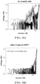
- FIG. 8A shows the current-voltage curves of as-wound coils. As-wound coils exhibited unpredictable current-voltage characteristics, as witnessed by voltage jumps and reduced critical current density. The coils were subsequently heated in a low-temperature oven at 185°C for 10 minutes in order to partially melt the solder and electrically connect the filaments. The current-voltage characteristics of the coils after the heat-treatment exhibited a marked improvement. The voltage spikes were practically absent and the critical current of three coils was within 10% of each other (see FIG. 8B ). This experiment demonstrates the improved stability due to current sharing in the electrically-coupled filaments.
- the filament connectivity was tested in a current transfer length experiment, schematically shown in FIG. 9 . Briefly, current was injected from one side of the filament stack and the current-voltage characteristics were recorded with the voltage probe placed at various distances from the current injection point. One would expect the current-voltage characteristics to stop changing once the voltage taps are sufficiently far away from the current injection point.
- the theory of current transfer between the normal metal and a high-temperature superconductor was developed by Levin et al. ( Levin, G., P. Barnes, and J. Bulmer, Current sharing between superconducting film and normal metal. Superconductor Science and Technology, 2007. 20(8): p. 757 ).
- FIG. 10 compares current-voltage characteristics of a 4-layer exfoliated cable with a 4- layer cable manufactured from standard 2 nd generation tape.
- the standard 2 nd generation tape incorporates an insulation substrate that prevents an effective current sharing between the filaments.
- the 4-layer exfoliated filament stack exhibits full current sharing at a distance of approximately 2 cm from the current injection point (see FIG. 10A ).
- the traditional 2G stack does not achieve current sharing even at a distance of 4 cm from the current lead (see FIG. 10B ).
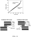
- the resistance between the exfoliated layers was measured by joining two pieces of 10 mm wide tape. The tapes were joined at the "copper side” and at the "YBCO side” as shown in FIG. 11 .
- the figure shows that the exfoliated layers have the same surface resistivity on both sides.
- the traditional 2G has very high resistance due to the current blocking action of the substrate.
- Dong et al. Dong Keun, P., et al., Analysis of a Joint Method Between Superconducting YBCO Coated Conductors. Applied Superconductivity, IEEE Transactions on, 2007. 17(2): p. 3266-3269 ) show that the contact resistance of two tapes joined by the substrate side is 25 times higher than the resistance of the tapes joined by the YBCO side.
Landscapes
- Engineering & Computer Science (AREA)
- Manufacturing & Machinery (AREA)
- Chemical & Material Sciences (AREA)
- Ceramic Engineering (AREA)
- Superconductors And Manufacturing Methods Therefor (AREA)
Claims (14)
- Un câble supraconducteur à haute température à filaments multiples, comprenant : une pluralité de filaments exfoliés empilés (301), chacun desdits filaments comprenant une couche supraconductrice (203) et une couche de métal de stabilisation (204) en l'absence d'une couche de substrat et d'une couche tampon, et dans lequel les filaments empilés adjacents sont soudés les uns aux autres avec une soudure à basse température et maintenus en contact mécanique uniforme les uns avec les autres afin de permettre la circulation ininterrompue du courant de la couche supraconductrice d'un filament vers la couche supraconductrice d'une couche adjacente, et dans lequel ledit contact mécanique uniforme assure un niveau de résistance de contact entre les filaments empilés adjacents inférieur à environ 10 µΩcm2.
- Le câble selon la revendication 1, dans lequel le niveau de résistance de contact entre les filaments empilés adjacents est inférieur à environ 1 µΩcm2.
- Le câble selon la revendication 2, dans lequel le niveau de résistance de contact entre les filaments empilés adjacents est inférieur à environ 0,01 µΩcm2.
- Le câble selon la revendication 1, dans lequel lesdits filaments empilés sont de préférence torsadés sur leur longueur.
- Le câble selon la revendication 4, dans lequel le pas de torsion est compris entre environ 5 mm et environ 80 mm.
- Le câble selon la revendication 1, dans lequel lesdits filaments empilés sont enveloppés en externe afin de fixer chacun desdits filaments sur les autres.
- Le câble selon la revendication 6, dans lequel lesdits filaments empilés sont enveloppés avec un fil en cuivre, nichrome ou acier inoxydable ou un fil synthétique.
- Le câble selon la revendication 1, dans lequel ladite soudure présente une épaisseur inférieure à environ 20 µm.
- Le câble selon la revendication 1, dans lequel la largeur de chacun desdits filaments est sensiblement constante et est comprise entre environ 0,1 mm et environ 3 mm.
- Le câble selon la revendication 9, dans lequel la hauteur desdits filaments empilés est sensiblement égale à la largeur desdits filaments afin d'obtenir un empilement ayant une section transversale sensiblement carrée.
- Le câble selon la revendication 1, dans lequel la largeur desdits filaments est variée afin d'obtenir un empilement ayant une section transversale sensiblement circulaire.
- Le câble selon la revendication 1, dans lequel un premier film métallique (302) est positionné sur le dessus desdits filaments empilés et un second film métallique (302) est positionné sur le bas desdits filaments empilés.
- Le câble selon la revendication 1, dans lequel un premier film métallique est positionné sur le dessus desdits filaments empilés et un second film métallique est positionné sur le bas desdits filaments empilés, et dans lequel lesdits filaments empilés sont enveloppés en externe afin de fixer chacun desdits filaments sur les autres, et dans lequel lesdits filaments empilés sont de préférence torsadés sur leur longueur, et dans lequel lesdits filaments empilés sont soudés les uns sur les autres.
- Une méthode de fabrication d'un câble supraconducteur à haute température à filaments multiples, comprenant les étapes de :empiler une pluralité de filaments exfoliés (301), dans lequel chacun desdits filaments comprend une couche supraconductrice (203) et une couche de métal de stabilisation (204) en l'absence d'une couche de substrat et d'une couche tampon, et dans lequel les filaments empilés adjacents sont en communication électrique les uns avec les autres de sorte que le courant puisse circuler de manière ininterrompue de la couche supraconductrice d'un filament vers la couche supraconductrice d'une couche adjacente ; etfixer les filaments empilés adjacents les uns sur les autres afin de maintenir un contact mécanique uniforme entre eux et d'obtenir un niveau de résistance de contact entre les filaments empilés adjacents inférieur à environ 10 µΩcm2, dans lequel lesdits filaments sont recouverts avec une soudure à basse température avant l'empilement, et dans lequel ladite étape de fixation comprend l'étape supplémentaire de chauffage desdits filaments empilés afin de refondre ladite soudure à basse température de façon à fixer les filaments empilés adjacents les uns sur les autres.
Applications Claiming Priority (2)
| Application Number | Priority Date | Filing Date | Title |
|---|---|---|---|
| US201762517452P | 2017-06-09 | 2017-06-09 | |
| PCT/US2018/036654 WO2018227083A1 (fr) | 2017-06-09 | 2018-06-08 | Câble supraconducteur flexible à haute température à filaments multiples |
Publications (3)
| Publication Number | Publication Date |
|---|---|
| EP3635754A1 EP3635754A1 (fr) | 2020-04-15 |
| EP3635754A4 EP3635754A4 (fr) | 2021-02-24 |
| EP3635754B1 true EP3635754B1 (fr) | 2024-11-27 |
Family
ID=64567299
Family Applications (1)
| Application Number | Title | Priority Date | Filing Date |
|---|---|---|---|
| EP18813976.0A Active EP3635754B1 (fr) | 2017-06-09 | 2018-06-08 | Câble supraconducteur flexible à haute température à filaments multiples |
Country Status (3)
| Country | Link |
|---|---|
| US (1) | US11877521B2 (fr) |
| EP (1) | EP3635754B1 (fr) |
| WO (1) | WO2018227083A1 (fr) |
Families Citing this family (6)
| Publication number | Priority date | Publication date | Assignee | Title |
|---|---|---|---|---|
| CN110010300B (zh) * | 2019-04-25 | 2020-07-14 | 上海交通大学 | 高温超导堆叠线扭绞装置及其工作方法 |
| US11887752B2 (en) * | 2020-10-26 | 2024-01-30 | The Texas A&M University System | Blocks-in-conduit cable using high-temperature superconducting tape |
| US12027361B2 (en) * | 2021-05-21 | 2024-07-02 | Microsoft Technology Licensing, Llc | High temperature superconductor-based interconnect systems with a lowered thermal load for interconnecting cryogenic electronics with non-cryogenic electronics |
| EP4246602A1 (fr) * | 2022-03-14 | 2023-09-20 | Theva Dünnschichttechnik GmbH | Bande supraconductrice à haute température hermétiquement étanche |
| WO2025120128A1 (fr) * | 2023-12-06 | 2025-06-12 | Subra A/S | Brin supraconducteur avec une pluralité de filaments torsadés |
| CN117954153A (zh) * | 2024-03-15 | 2024-04-30 | 重庆科宝电缆股份有限公司 | 一种耐候耐久环保型光伏电缆 |
Family Cites Families (27)
| Publication number | Priority date | Publication date | Assignee | Title |
|---|---|---|---|---|
| CH483133A (de) | 1969-01-31 | 1969-12-15 | Oerlikon Maschf | Verfahren zur Herstellung einer Verbindung zwischen stabilisierten Supraleitern |
| US5149681A (en) | 1990-05-14 | 1992-09-22 | General Atomics | Melt texturing of long superconductor fibers |
| JPH08264039A (ja) * | 1995-01-26 | 1996-10-11 | Japan Atom Energy Res Inst | 超電導ケーブル |
| JP3658844B2 (ja) * | 1996-03-26 | 2005-06-08 | 住友電気工業株式会社 | 酸化物超電導線材およびその製造方法ならびにそれを用いた酸化物超電導撚線および導体 |
| US6828507B1 (en) | 1999-07-23 | 2004-12-07 | American Superconductor Corporation | Enhanced high temperature coated superconductors joined at a cap layer |
| JP2005029772A (ja) | 2003-07-11 | 2005-02-03 | Nexpress Solutions Inc | 低ぬれ性のフルオロカーボン熱可塑性ランダムコポリマー製のローラー被覆用組成物 |
| US7816303B2 (en) | 2004-10-01 | 2010-10-19 | American Superconductor Corporation | Architecture for high temperature superconductor wire |
| US7820097B2 (en) | 2004-11-24 | 2010-10-26 | Ncc Nano, Llc | Electrical, plating and catalytic uses of metal nanomaterial compositions |
| US7071148B1 (en) | 2005-04-08 | 2006-07-04 | Superpower, Inc. | Joined superconductive articles |
| US8030246B2 (en) * | 2006-07-21 | 2011-10-04 | American Superconductor Corporation | Low resistance splice for high temperature superconductor wires |
| ES2399842T3 (es) * | 2006-07-21 | 2013-04-03 | American Superconductor Corporation | Conductores flexibles compactos, de gran amperaje, que contienen cintas superconductoras de alta temperatura |
| US7893006B2 (en) | 2007-03-23 | 2011-02-22 | American Superconductor Corporation | Systems and methods for solution-based deposition of metallic cap layers for high temperature superconductor wires |
| KR20080089730A (ko) | 2007-04-02 | 2008-10-08 | 삼성전자주식회사 | 편광판의 제거 장치 및 그 방법 |
| EP2168179B1 (fr) | 2007-06-22 | 2014-08-13 | NKT Cables Ultera A/S | Jonction d'éléments supraconducteurs |
| US7676187B2 (en) | 2007-09-27 | 2010-03-09 | Xerox Corporation | Enhanced fuser stripping system |
| US8731629B2 (en) | 2008-03-28 | 2014-05-20 | American Superconductor Corporation | Interface device for a high temperature superconductor degaussing system junction box |
| US8195260B2 (en) | 2008-07-23 | 2012-06-05 | American Superconductor Corporation | Two-sided splice for high temperature superconductor laminated wires |
| US8437819B2 (en) | 2008-10-08 | 2013-05-07 | Massachusetts Institute Of Technology | Superconductor cable |
| US8938278B2 (en) | 2011-02-18 | 2015-01-20 | The Regents Of The University Of Colorado | Superconducting cables and methods of making the same |
| EP2490273B1 (fr) | 2011-02-18 | 2013-05-01 | Bruker HTS GmbH | Procédé de fabrication d'une bande revêtue de HTS avec un découpage au faisceau laser |
| GB2498961A (en) | 2012-02-01 | 2013-08-07 | Siemens Plc | Methods of joining superconducting wires |
| NZ620910A (en) | 2012-06-11 | 2016-04-29 | Fujikura Ltd | Oxide superconducting wire and superconducting coil |
| KR101410841B1 (ko) | 2012-11-26 | 2014-06-23 | 한국전기연구원 | 고온 초전도 선재 |
| EP2955727B1 (fr) | 2013-03-15 | 2019-04-10 | Furukawa Electric Co., Ltd. | Procédé permettant de fabriquer un conducteur supraconducteur et conducteur supraconducteur |
| US10109609B2 (en) * | 2014-01-13 | 2018-10-23 | Infineon Technologies Austria Ag | Connection structure and electronic component |
| US9908158B2 (en) | 2014-03-10 | 2018-03-06 | Ametek, Inc. | Air flow mechanism for image capture and vision systems |
| DE102015010636A1 (de) * | 2015-08-12 | 2017-02-16 | Karlsruher Institut für Technologie | Supraleitfähiger Leiter und Verwendung des supraleitfähigen Leiters |
-
2018
- 2018-06-08 EP EP18813976.0A patent/EP3635754B1/fr active Active
- 2018-06-08 WO PCT/US2018/036654 patent/WO2018227083A1/fr not_active Ceased
- 2018-06-08 US US16/620,636 patent/US11877521B2/en active Active
Also Published As
| Publication number | Publication date |
|---|---|
| US11877521B2 (en) | 2024-01-16 |
| EP3635754A1 (fr) | 2020-04-15 |
| US20200194657A1 (en) | 2020-06-18 |
| EP3635754A4 (fr) | 2021-02-24 |
| WO2018227083A1 (fr) | 2018-12-13 |
Similar Documents
| Publication | Publication Date | Title |
|---|---|---|
| EP3635754B1 (fr) | Câble supraconducteur flexible à haute température à filaments multiples | |
| KR102683995B1 (ko) | 제2세대 초전도성 필라멘트와 케이블 | |
| US8716188B2 (en) | Structure to reduce electroplated stabilizer content | |
| EP0371410B1 (fr) | Connexion de supraconducteurs oxydés ayant une température critique élevée | |
| US11783968B2 (en) | Cabling method of superconducting flat wires | |
| JP5568361B2 (ja) | 超電導線材の電極部接合構造、超電導線材、及び超電導コイル | |
| EP2324482A1 (fr) | Joint double face pour fils supraconducteurs en stratifié pour hautes températures | |
| US6844064B1 (en) | Method of manufacturing oxide superconducting wire, oxide superconducting wire, superconducting coil and superconducting apparatus | |
| US20080210454A1 (en) | Composite Superconductor Cable Produced by Transposing Planar Subconductors | |
| JP6101490B2 (ja) | 酸化物超電導線材の接続構造体及び超電導機器 | |
| EP1166370B1 (fr) | Materiau composite limiteur de courant | |
| Solovyov et al. | Electromechanical properties of 1-mm-wide superconducting cables comprised of exfoliated YBCO filaments | |
| US20250232896A1 (en) | Hts tape with improved transverse conductance | |
| EP3540795A1 (fr) | Supraconducteur de type bande ayant une pluralité de structures barrières allongées | |
| NZ745190B2 (en) | Second generation superconducting filaments and cable | |
| Scanlan et al. | Multifilamentary Nb 3 Sn for superconducting generator applications | |
| US20200194155A1 (en) | Superconducting wire and superconducting coil | |
| JPH10188696A (ja) | 酸化物超電導線材及びその接合方法 | |
| JP2022139398A (ja) | 希土類系酸化物超伝導多芯線材、および、その製造方法 | |
| AU2009274080B2 (en) | Two-sided splice for high temperature superconductor laminated wires | |
| US20070191232A1 (en) | Superconductor Wire Material Having Structure For Inhibiting Crack, Superconductor Power Cable Using The Same And Manufacturing Method Thereof | |
| MXPA00002588A (en) | Fault current limiting superconducting coil |
Legal Events
| Date | Code | Title | Description |
|---|---|---|---|
| STAA | Information on the status of an ep patent application or granted ep patent |
Free format text: STATUS: THE INTERNATIONAL PUBLICATION HAS BEEN MADE |
|
| PUAI | Public reference made under article 153(3) epc to a published international application that has entered the european phase |
Free format text: ORIGINAL CODE: 0009012 |
|
| STAA | Information on the status of an ep patent application or granted ep patent |
Free format text: STATUS: REQUEST FOR EXAMINATION WAS MADE |
|
| 17P | Request for examination filed |
Effective date: 20191212 |
|
| AK | Designated contracting states |
Kind code of ref document: A1 Designated state(s): AL AT BE BG CH CY CZ DE DK EE ES FI FR GB GR HR HU IE IS IT LI LT LU LV MC MK MT NL NO PL PT RO RS SE SI SK SM TR |
|
| AX | Request for extension of the european patent |
Extension state: BA ME |
|
| DAV | Request for validation of the european patent (deleted) | ||
| DAX | Request for extension of the european patent (deleted) | ||
| A4 | Supplementary search report drawn up and despatched |
Effective date: 20210127 |
|
| RIC1 | Information provided on ipc code assigned before grant |
Ipc: H01L 39/14 20060101AFI20210121BHEP Ipc: H01L 39/24 20060101ALI20210121BHEP |
|
| REG | Reference to a national code |
Ref legal event code: R079 Ipc: H10N0060010000 Ref country code: DE Ref legal event code: R079 Ref document number: 602018077043 Country of ref document: DE Free format text: PREVIOUS MAIN CLASS: H01B0012080000 Ipc: H10N0060010000 |
|
| GRAP | Despatch of communication of intention to grant a patent |
Free format text: ORIGINAL CODE: EPIDOSNIGR1 |
|
| STAA | Information on the status of an ep patent application or granted ep patent |
Free format text: STATUS: GRANT OF PATENT IS INTENDED |
|
| RIC1 | Information provided on ipc code assigned before grant |
Ipc: H10N 60/20 20230101ALI20240614BHEP Ipc: H10N 60/01 20230101AFI20240614BHEP |
|
| INTG | Intention to grant announced |
Effective date: 20240722 |
|
| RAP3 | Party data changed (applicant data changed or rights of an application transferred) |
Owner name: BROOKHAVEN TECHNOLOGY GROUP, INC. |
|
| GRAS | Grant fee paid |
Free format text: ORIGINAL CODE: EPIDOSNIGR3 |
|
| GRAA | (expected) grant |
Free format text: ORIGINAL CODE: 0009210 |
|
| STAA | Information on the status of an ep patent application or granted ep patent |
Free format text: STATUS: THE PATENT HAS BEEN GRANTED |
|
| AK | Designated contracting states |
Kind code of ref document: B1 Designated state(s): AL AT BE BG CH CY CZ DE DK EE ES FI FR GB GR HR HU IE IS IT LI LT LU LV MC MK MT NL NO PL PT RO RS SE SI SK SM TR |
|
| REG | Reference to a national code |
Ref country code: GB Ref legal event code: FG4D |
|
| REG | Reference to a national code |
Ref country code: CH Ref legal event code: EP |
|
| REG | Reference to a national code |
Ref country code: IE Ref legal event code: FG4D |
|
| REG | Reference to a national code |
Ref country code: DE Ref legal event code: R096 Ref document number: 602018077043 Country of ref document: DE |
|
| REG | Reference to a national code |
Ref country code: NL Ref legal event code: FP |
|
| REG | Reference to a national code |
Ref country code: LT Ref legal event code: MG9D |
|
| PG25 | Lapsed in a contracting state [announced via postgrant information from national office to epo] |
Ref country code: PT Free format text: LAPSE BECAUSE OF FAILURE TO SUBMIT A TRANSLATION OF THE DESCRIPTION OR TO PAY THE FEE WITHIN THE PRESCRIBED TIME-LIMIT Effective date: 20250327 Ref country code: IS Free format text: LAPSE BECAUSE OF FAILURE TO SUBMIT A TRANSLATION OF THE DESCRIPTION OR TO PAY THE FEE WITHIN THE PRESCRIBED TIME-LIMIT Effective date: 20250327 Ref country code: HR Free format text: LAPSE BECAUSE OF FAILURE TO SUBMIT A TRANSLATION OF THE DESCRIPTION OR TO PAY THE FEE WITHIN THE PRESCRIBED TIME-LIMIT Effective date: 20241127 |
|
| PG25 | Lapsed in a contracting state [announced via postgrant information from national office to epo] |
Ref country code: FI Free format text: LAPSE BECAUSE OF FAILURE TO SUBMIT A TRANSLATION OF THE DESCRIPTION OR TO PAY THE FEE WITHIN THE PRESCRIBED TIME-LIMIT Effective date: 20241127 |
|
| REG | Reference to a national code |
Ref country code: AT Ref legal event code: MK05 Ref document number: 1747054 Country of ref document: AT Kind code of ref document: T Effective date: 20241127 |
|
| PG25 | Lapsed in a contracting state [announced via postgrant information from national office to epo] |
Ref country code: BG Free format text: LAPSE BECAUSE OF FAILURE TO SUBMIT A TRANSLATION OF THE DESCRIPTION OR TO PAY THE FEE WITHIN THE PRESCRIBED TIME-LIMIT Effective date: 20241127 |
|
| PG25 | Lapsed in a contracting state [announced via postgrant information from national office to epo] |
Ref country code: ES Free format text: LAPSE BECAUSE OF FAILURE TO SUBMIT A TRANSLATION OF THE DESCRIPTION OR TO PAY THE FEE WITHIN THE PRESCRIBED TIME-LIMIT Effective date: 20241127 |
|
| PG25 | Lapsed in a contracting state [announced via postgrant information from national office to epo] |
Ref country code: NO Free format text: LAPSE BECAUSE OF FAILURE TO SUBMIT A TRANSLATION OF THE DESCRIPTION OR TO PAY THE FEE WITHIN THE PRESCRIBED TIME-LIMIT Effective date: 20250227 |
|
| PG25 | Lapsed in a contracting state [announced via postgrant information from national office to epo] |
Ref country code: GR Free format text: LAPSE BECAUSE OF FAILURE TO SUBMIT A TRANSLATION OF THE DESCRIPTION OR TO PAY THE FEE WITHIN THE PRESCRIBED TIME-LIMIT Effective date: 20250228 Ref country code: LV Free format text: LAPSE BECAUSE OF FAILURE TO SUBMIT A TRANSLATION OF THE DESCRIPTION OR TO PAY THE FEE WITHIN THE PRESCRIBED TIME-LIMIT Effective date: 20241127 Ref country code: AT Free format text: LAPSE BECAUSE OF FAILURE TO SUBMIT A TRANSLATION OF THE DESCRIPTION OR TO PAY THE FEE WITHIN THE PRESCRIBED TIME-LIMIT Effective date: 20241127 |
|
| PG25 | Lapsed in a contracting state [announced via postgrant information from national office to epo] |
Ref country code: PL Free format text: LAPSE BECAUSE OF FAILURE TO SUBMIT A TRANSLATION OF THE DESCRIPTION OR TO PAY THE FEE WITHIN THE PRESCRIBED TIME-LIMIT Effective date: 20241127 |
|
| PG25 | Lapsed in a contracting state [announced via postgrant information from national office to epo] |
Ref country code: RS Free format text: LAPSE BECAUSE OF FAILURE TO SUBMIT A TRANSLATION OF THE DESCRIPTION OR TO PAY THE FEE WITHIN THE PRESCRIBED TIME-LIMIT Effective date: 20250227 |
|
| PG25 | Lapsed in a contracting state [announced via postgrant information from national office to epo] |
Ref country code: SM Free format text: LAPSE BECAUSE OF FAILURE TO SUBMIT A TRANSLATION OF THE DESCRIPTION OR TO PAY THE FEE WITHIN THE PRESCRIBED TIME-LIMIT Effective date: 20241127 |
|
| PGFP | Annual fee paid to national office [announced via postgrant information from national office to epo] |
Ref country code: DE Payment date: 20250505 Year of fee payment: 8 |
|
| PG25 | Lapsed in a contracting state [announced via postgrant information from national office to epo] |
Ref country code: DK Free format text: LAPSE BECAUSE OF FAILURE TO SUBMIT A TRANSLATION OF THE DESCRIPTION OR TO PAY THE FEE WITHIN THE PRESCRIBED TIME-LIMIT Effective date: 20241127 |
|
| PGFP | Annual fee paid to national office [announced via postgrant information from national office to epo] |
Ref country code: GB Payment date: 20250620 Year of fee payment: 8 |
|
| PGFP | Annual fee paid to national office [announced via postgrant information from national office to epo] |
Ref country code: NL Payment date: 20250618 Year of fee payment: 8 |
|
| PG25 | Lapsed in a contracting state [announced via postgrant information from national office to epo] |
Ref country code: EE Free format text: LAPSE BECAUSE OF FAILURE TO SUBMIT A TRANSLATION OF THE DESCRIPTION OR TO PAY THE FEE WITHIN THE PRESCRIBED TIME-LIMIT Effective date: 20241127 |
|
| PGFP | Annual fee paid to national office [announced via postgrant information from national office to epo] |
Ref country code: FR Payment date: 20250627 Year of fee payment: 8 |
|
| PG25 | Lapsed in a contracting state [announced via postgrant information from national office to epo] |
Ref country code: RO Free format text: LAPSE BECAUSE OF FAILURE TO SUBMIT A TRANSLATION OF THE DESCRIPTION OR TO PAY THE FEE WITHIN THE PRESCRIBED TIME-LIMIT Effective date: 20241127 |
|
| PG25 | Lapsed in a contracting state [announced via postgrant information from national office to epo] |
Ref country code: SK Free format text: LAPSE BECAUSE OF FAILURE TO SUBMIT A TRANSLATION OF THE DESCRIPTION OR TO PAY THE FEE WITHIN THE PRESCRIBED TIME-LIMIT Effective date: 20241127 |
|
| PG25 | Lapsed in a contracting state [announced via postgrant information from national office to epo] |
Ref country code: CZ Free format text: LAPSE BECAUSE OF FAILURE TO SUBMIT A TRANSLATION OF THE DESCRIPTION OR TO PAY THE FEE WITHIN THE PRESCRIBED TIME-LIMIT Effective date: 20241127 |
|
| PG25 | Lapsed in a contracting state [announced via postgrant information from national office to epo] |
Ref country code: IT Free format text: LAPSE BECAUSE OF FAILURE TO SUBMIT A TRANSLATION OF THE DESCRIPTION OR TO PAY THE FEE WITHIN THE PRESCRIBED TIME-LIMIT Effective date: 20241127 |
|
| REG | Reference to a national code |
Ref country code: DE Ref legal event code: R097 Ref document number: 602018077043 Country of ref document: DE |
|
| PG25 | Lapsed in a contracting state [announced via postgrant information from national office to epo] |
Ref country code: SE Free format text: LAPSE BECAUSE OF FAILURE TO SUBMIT A TRANSLATION OF THE DESCRIPTION OR TO PAY THE FEE WITHIN THE PRESCRIBED TIME-LIMIT Effective date: 20241127 |
|
| PLBE | No opposition filed within time limit |
Free format text: ORIGINAL CODE: 0009261 |
|
| STAA | Information on the status of an ep patent application or granted ep patent |
Free format text: STATUS: NO OPPOSITION FILED WITHIN TIME LIMIT |
|
| REG | Reference to a national code |
Ref country code: CH Ref legal event code: L10 Free format text: ST27 STATUS EVENT CODE: U-0-0-L10-L00 (AS PROVIDED BY THE NATIONAL OFFICE) Effective date: 20251008 |
|
| 26N | No opposition filed |
Effective date: 20250828 |
|
| REG | Reference to a national code |
Ref country code: CH Ref legal event code: H13 Free format text: ST27 STATUS EVENT CODE: U-0-0-H10-H13 (AS PROVIDED BY THE NATIONAL OFFICE) Effective date: 20260127 |
|
| PG25 | Lapsed in a contracting state [announced via postgrant information from national office to epo] |
Ref country code: MC Free format text: LAPSE BECAUSE OF FAILURE TO SUBMIT A TRANSLATION OF THE DESCRIPTION OR TO PAY THE FEE WITHIN THE PRESCRIBED TIME-LIMIT Effective date: 20241127 |
|
| PG25 | Lapsed in a contracting state [announced via postgrant information from national office to epo] |
Ref country code: LU Free format text: LAPSE BECAUSE OF NON-PAYMENT OF DUE FEES Effective date: 20250608 |
|
| REG | Reference to a national code |
Ref country code: BE Ref legal event code: MM Effective date: 20250630 |
|
| PG25 | Lapsed in a contracting state [announced via postgrant information from national office to epo] |
Ref country code: IE Free format text: LAPSE BECAUSE OF NON-PAYMENT OF DUE FEES Effective date: 20250608 |
|
| PG25 | Lapsed in a contracting state [announced via postgrant information from national office to epo] |
Ref country code: BE Free format text: LAPSE BECAUSE OF NON-PAYMENT OF DUE FEES Effective date: 20250630 |
|
| PG25 | Lapsed in a contracting state [announced via postgrant information from national office to epo] |
Ref country code: CH Free format text: LAPSE BECAUSE OF NON-PAYMENT OF DUE FEES Effective date: 20250630 |