EP3636726B1 - Matériau hôte multicomposant et dispositif électroluminescent organique comprenant ce matériau - Google Patents
Matériau hôte multicomposant et dispositif électroluminescent organique comprenant ce matériau Download PDFInfo
- Publication number
- EP3636726B1 EP3636726B1 EP19209591.7A EP19209591A EP3636726B1 EP 3636726 B1 EP3636726 B1 EP 3636726B1 EP 19209591 A EP19209591 A EP 19209591A EP 3636726 B1 EP3636726 B1 EP 3636726B1
- Authority
- EP
- European Patent Office
- Prior art keywords
- substituted
- unsubstituted
- alkyl
- mono
- arylsilyl
- Prior art date
- Legal status (The legal status is an assumption and is not a legal conclusion. Google has not performed a legal analysis and makes no representation as to the accuracy of the status listed.)
- Active
Links
- 0 CC1*=*=C*1 Chemical compound CC1*=*=C*1 0.000 description 19
- ARDQEBPQBWHYOI-UHFFFAOYSA-N C(N1)=C(C2=NC(c3cc(cccc4)c4cc3)NC(c3cc(cccc4)c4cc3)[N-]2)[N-]C1[n]1c(cc(c(c2ccccc22)c3)[n]2-c2ccccc2)c3c2c1cccc2 Chemical compound C(N1)=C(C2=NC(c3cc(cccc4)c4cc3)NC(c3cc(cccc4)c4cc3)[N-]2)[N-]C1[n]1c(cc(c(c2ccccc22)c3)[n]2-c2ccccc2)c3c2c1cccc2 ARDQEBPQBWHYOI-UHFFFAOYSA-N 0.000 description 1
- FJKKHAMSLVQAMI-UHFFFAOYSA-N C(N1)=C(C2NC(c3ccccc3)NC(c(cc3)ccc3-c3ccccc3)[N-]2)[N-]C1[n]1c(cc(c(c2ccccc22)c3)[n]2-c2ccccc2)c3c2ccccc12 Chemical compound C(N1)=C(C2NC(c3ccccc3)NC(c(cc3)ccc3-c3ccccc3)[N-]2)[N-]C1[n]1c(cc(c(c2ccccc22)c3)[n]2-c2ccccc2)c3c2ccccc12 FJKKHAMSLVQAMI-UHFFFAOYSA-N 0.000 description 1
- MSJNBBOWQLCAHX-PYXZATOCSA-N C/C=C(/C1NC(c2cccc3c2cccc3)NC(c2ccccc2)[N-]1)\[N-]C([C@H]1c(cc(c(c2c3cccc2)c2)[n]3-c3ccccc3)c2-c2c1cccc2)N Chemical compound C/C=C(/C1NC(c2cccc3c2cccc3)NC(c2ccccc2)[N-]1)\[N-]C([C@H]1c(cc(c(c2c3cccc2)c2)[n]3-c3ccccc3)c2-c2c1cccc2)N MSJNBBOWQLCAHX-PYXZATOCSA-N 0.000 description 1
- SLYMWRUGLJVNSF-UHFFFAOYSA-N C1NC([n]2c(cc(c(c3ccccc33)c4)[n]3-c3ccccc3)c4c3ccccc23)=CC(C2NC(c3ccccc3)=NC(c(cc3)ccc3-c3ccccc3)[N-]2)=C1 Chemical compound C1NC([n]2c(cc(c(c3ccccc33)c4)[n]3-c3ccccc3)c4c3ccccc23)=CC(C2NC(c3ccccc3)=NC(c(cc3)ccc3-c3ccccc3)[N-]2)=C1 SLYMWRUGLJVNSF-UHFFFAOYSA-N 0.000 description 1
- AFDMODCXODAXLC-UHFFFAOYSA-N N=Cc1ccccc1 Chemical compound N=Cc1ccccc1 AFDMODCXODAXLC-UHFFFAOYSA-N 0.000 description 1
- HZCGENLPIIFINT-UHFFFAOYSA-N c([nH]1)c(C2=NC(c3ccccc3)NC(c3ccccc3)[N-]2)nc1-[n]1c(cc(c(c2c3cccc2)c2)[n]3-c3ccccc3)c2c2c1cccc2 Chemical compound c([nH]1)c(C2=NC(c3ccccc3)NC(c3ccccc3)[N-]2)nc1-[n]1c(cc(c(c2c3cccc2)c2)[n]3-c3ccccc3)c2c2c1cccc2 HZCGENLPIIFINT-UHFFFAOYSA-N 0.000 description 1
- ULBKRQFAQFIDRO-UHFFFAOYSA-N c(c(C1=NC(c2cc(cccc3)c3cc2)NC(c2cc(cccc3)c3cc2)[N-]1)c[nH]1)c1-[n]1c(cc(c(c2ccccc22)c3)[n]2-c2ccccc2)c3c2c1cccc2 Chemical compound c(c(C1=NC(c2cc(cccc3)c3cc2)NC(c2cc(cccc3)c3cc2)[N-]1)c[nH]1)c1-[n]1c(cc(c(c2ccccc22)c3)[n]2-c2ccccc2)c3c2c1cccc2 ULBKRQFAQFIDRO-UHFFFAOYSA-N 0.000 description 1
- XYJOZTUZLZNOCK-UHFFFAOYSA-N c(c(C1NC(c2cccc3c2cccc3)NC(c2ccccc2)[N-]1)c[nH]1)c1-[n]1c(cc(c(c2c3cccc2)c2)[n]3-c3ccccc3)c2c2c1cccc2 Chemical compound c(c(C1NC(c2cccc3c2cccc3)NC(c2ccccc2)[N-]1)c[nH]1)c1-[n]1c(cc(c(c2c3cccc2)c2)[n]3-c3ccccc3)c2c2c1cccc2 XYJOZTUZLZNOCK-UHFFFAOYSA-N 0.000 description 1
- KFRIOXRVCKTKMW-UHFFFAOYSA-N c(c(C1NC(c2ccccc2)NC(c2ccccc2)[N-]1)c[nH]1)c1-[n](c(cccc1)c1c1c2)c1cc1c2c(cccc2)c2[n]1-c1ccccc1 Chemical compound c(c(C1NC(c2ccccc2)NC(c2ccccc2)[N-]1)c[nH]1)c1-[n](c(cccc1)c1c1c2)c1cc1c2c(cccc2)c2[n]1-c1ccccc1 KFRIOXRVCKTKMW-UHFFFAOYSA-N 0.000 description 1
- YHDAXWKRAIPAKX-UHFFFAOYSA-N c1ccc(C2NC(c3cc(cccc4)c4cc3)N=C(C([N-]3)=CC=NC3[n]3c(cc(c(c4c5cccc4)c4)[n]5-c5ccccc5)c4c4c3cccc4)[N-]2)cc1 Chemical compound c1ccc(C2NC(c3cc(cccc4)c4cc3)N=C(C([N-]3)=CC=NC3[n]3c(cc(c(c4c5cccc4)c4)[n]5-c5ccccc5)c4c4c3cccc4)[N-]2)cc1 YHDAXWKRAIPAKX-UHFFFAOYSA-N 0.000 description 1
- UPWVMADBDRIZHP-UHFFFAOYSA-N c1ccc(C2NC(c3cc(cccc4)c4cc3)N=C(c3ccnc(-[n]4c(cc(c(c5c6cccc5)c5)[n]6-c6ccccc6)c5c5ccccc45)c3)[N-]2)cc1 Chemical compound c1ccc(C2NC(c3cc(cccc4)c4cc3)N=C(c3ccnc(-[n]4c(cc(c(c5c6cccc5)c5)[n]6-c6ccccc6)c5c5ccccc45)c3)[N-]2)cc1 UPWVMADBDRIZHP-UHFFFAOYSA-N 0.000 description 1
Classifications
-
- H—ELECTRICITY
- H10—SEMICONDUCTOR DEVICES; ELECTRIC SOLID-STATE DEVICES NOT OTHERWISE PROVIDED FOR
- H10K—ORGANIC ELECTRIC SOLID-STATE DEVICES
- H10K50/00—Organic light-emitting devices
- H10K50/10—OLEDs or polymer light-emitting diodes [PLED]
- H10K50/11—OLEDs or polymer light-emitting diodes [PLED] characterised by the electroluminescent [EL] layers
- H10K50/12—OLEDs or polymer light-emitting diodes [PLED] characterised by the electroluminescent [EL] layers comprising dopants
-
- C—CHEMISTRY; METALLURGY
- C09—DYES; PAINTS; POLISHES; NATURAL RESINS; ADHESIVES; COMPOSITIONS NOT OTHERWISE PROVIDED FOR; APPLICATIONS OF MATERIALS NOT OTHERWISE PROVIDED FOR
- C09K—MATERIALS FOR MISCELLANEOUS APPLICATIONS, NOT PROVIDED FOR ELSEWHERE
- C09K11/00—Luminescent materials, e.g. electroluminescent or chemiluminescent
- C09K11/02—Use of particular materials as binders, particle coatings or suspension media therefor
- C09K11/025—Use of particular materials as binders, particle coatings or suspension media therefor non-luminescent particle coatings or suspension media
-
- C—CHEMISTRY; METALLURGY
- C09—DYES; PAINTS; POLISHES; NATURAL RESINS; ADHESIVES; COMPOSITIONS NOT OTHERWISE PROVIDED FOR; APPLICATIONS OF MATERIALS NOT OTHERWISE PROVIDED FOR
- C09K—MATERIALS FOR MISCELLANEOUS APPLICATIONS, NOT PROVIDED FOR ELSEWHERE
- C09K11/00—Luminescent materials, e.g. electroluminescent or chemiluminescent
- C09K11/06—Luminescent materials, e.g. electroluminescent or chemiluminescent containing organic luminescent materials
-
- H—ELECTRICITY
- H10—SEMICONDUCTOR DEVICES; ELECTRIC SOLID-STATE DEVICES NOT OTHERWISE PROVIDED FOR
- H10K—ORGANIC ELECTRIC SOLID-STATE DEVICES
- H10K50/00—Organic light-emitting devices
- H10K50/10—OLEDs or polymer light-emitting diodes [PLED]
- H10K50/11—OLEDs or polymer light-emitting diodes [PLED] characterised by the electroluminescent [EL] layers
-
- H—ELECTRICITY
- H10—SEMICONDUCTOR DEVICES; ELECTRIC SOLID-STATE DEVICES NOT OTHERWISE PROVIDED FOR
- H10K—ORGANIC ELECTRIC SOLID-STATE DEVICES
- H10K85/00—Organic materials used in the body or electrodes of devices covered by this subclass
- H10K85/30—Coordination compounds
- H10K85/341—Transition metal complexes, e.g. Ru(II)polypyridine complexes
- H10K85/342—Transition metal complexes, e.g. Ru(II)polypyridine complexes comprising iridium
-
- H—ELECTRICITY
- H10—SEMICONDUCTOR DEVICES; ELECTRIC SOLID-STATE DEVICES NOT OTHERWISE PROVIDED FOR
- H10K—ORGANIC ELECTRIC SOLID-STATE DEVICES
- H10K85/00—Organic materials used in the body or electrodes of devices covered by this subclass
- H10K85/40—Organosilicon compounds, e.g. TIPS pentacene
-
- H—ELECTRICITY
- H10—SEMICONDUCTOR DEVICES; ELECTRIC SOLID-STATE DEVICES NOT OTHERWISE PROVIDED FOR
- H10K—ORGANIC ELECTRIC SOLID-STATE DEVICES
- H10K85/00—Organic materials used in the body or electrodes of devices covered by this subclass
- H10K85/60—Organic compounds having low molecular weight
- H10K85/615—Polycyclic condensed aromatic hydrocarbons, e.g. anthracene
-
- H—ELECTRICITY
- H10—SEMICONDUCTOR DEVICES; ELECTRIC SOLID-STATE DEVICES NOT OTHERWISE PROVIDED FOR
- H10K—ORGANIC ELECTRIC SOLID-STATE DEVICES
- H10K85/00—Organic materials used in the body or electrodes of devices covered by this subclass
- H10K85/60—Organic compounds having low molecular weight
- H10K85/615—Polycyclic condensed aromatic hydrocarbons, e.g. anthracene
- H10K85/626—Polycyclic condensed aromatic hydrocarbons, e.g. anthracene containing more than one polycyclic condensed aromatic rings, e.g. bis-anthracene
-
- H—ELECTRICITY
- H10—SEMICONDUCTOR DEVICES; ELECTRIC SOLID-STATE DEVICES NOT OTHERWISE PROVIDED FOR
- H10K—ORGANIC ELECTRIC SOLID-STATE DEVICES
- H10K85/00—Organic materials used in the body or electrodes of devices covered by this subclass
- H10K85/60—Organic compounds having low molecular weight
- H10K85/649—Aromatic compounds comprising a hetero atom
- H10K85/654—Aromatic compounds comprising a hetero atom comprising only nitrogen as heteroatom
-
- H—ELECTRICITY
- H10—SEMICONDUCTOR DEVICES; ELECTRIC SOLID-STATE DEVICES NOT OTHERWISE PROVIDED FOR
- H10K—ORGANIC ELECTRIC SOLID-STATE DEVICES
- H10K85/00—Organic materials used in the body or electrodes of devices covered by this subclass
- H10K85/60—Organic compounds having low molecular weight
- H10K85/649—Aromatic compounds comprising a hetero atom
- H10K85/657—Polycyclic condensed heteroaromatic hydrocarbons
-
- H—ELECTRICITY
- H10—SEMICONDUCTOR DEVICES; ELECTRIC SOLID-STATE DEVICES NOT OTHERWISE PROVIDED FOR
- H10K—ORGANIC ELECTRIC SOLID-STATE DEVICES
- H10K85/00—Organic materials used in the body or electrodes of devices covered by this subclass
- H10K85/60—Organic compounds having low molecular weight
- H10K85/649—Aromatic compounds comprising a hetero atom
- H10K85/657—Polycyclic condensed heteroaromatic hydrocarbons
- H10K85/6572—Polycyclic condensed heteroaromatic hydrocarbons comprising only nitrogen in the heteroaromatic polycondensed ring system, e.g. phenanthroline or carbazole
-
- H—ELECTRICITY
- H10—SEMICONDUCTOR DEVICES; ELECTRIC SOLID-STATE DEVICES NOT OTHERWISE PROVIDED FOR
- H10K—ORGANIC ELECTRIC SOLID-STATE DEVICES
- H10K85/00—Organic materials used in the body or electrodes of devices covered by this subclass
- H10K85/60—Organic compounds having low molecular weight
- H10K85/649—Aromatic compounds comprising a hetero atom
- H10K85/657—Polycyclic condensed heteroaromatic hydrocarbons
- H10K85/6574—Polycyclic condensed heteroaromatic hydrocarbons comprising only oxygen in the heteroaromatic polycondensed ring system, e.g. cumarine dyes
-
- H—ELECTRICITY
- H10—SEMICONDUCTOR DEVICES; ELECTRIC SOLID-STATE DEVICES NOT OTHERWISE PROVIDED FOR
- H10K—ORGANIC ELECTRIC SOLID-STATE DEVICES
- H10K85/00—Organic materials used in the body or electrodes of devices covered by this subclass
- H10K85/60—Organic compounds having low molecular weight
- H10K85/649—Aromatic compounds comprising a hetero atom
- H10K85/657—Polycyclic condensed heteroaromatic hydrocarbons
- H10K85/6576—Polycyclic condensed heteroaromatic hydrocarbons comprising only sulfur in the heteroaromatic polycondensed ring system, e.g. benzothiophene
-
- C—CHEMISTRY; METALLURGY
- C09—DYES; PAINTS; POLISHES; NATURAL RESINS; ADHESIVES; COMPOSITIONS NOT OTHERWISE PROVIDED FOR; APPLICATIONS OF MATERIALS NOT OTHERWISE PROVIDED FOR
- C09K—MATERIALS FOR MISCELLANEOUS APPLICATIONS, NOT PROVIDED FOR ELSEWHERE
- C09K2211/00—Chemical nature of organic luminescent or tenebrescent compounds
- C09K2211/10—Non-macromolecular compounds
- C09K2211/1003—Carbocyclic compounds
- C09K2211/1011—Condensed systems
-
- C—CHEMISTRY; METALLURGY
- C09—DYES; PAINTS; POLISHES; NATURAL RESINS; ADHESIVES; COMPOSITIONS NOT OTHERWISE PROVIDED FOR; APPLICATIONS OF MATERIALS NOT OTHERWISE PROVIDED FOR
- C09K—MATERIALS FOR MISCELLANEOUS APPLICATIONS, NOT PROVIDED FOR ELSEWHERE
- C09K2211/00—Chemical nature of organic luminescent or tenebrescent compounds
- C09K2211/10—Non-macromolecular compounds
- C09K2211/1018—Heterocyclic compounds
- C09K2211/1025—Heterocyclic compounds characterised by ligands
- C09K2211/1029—Heterocyclic compounds characterised by ligands containing one nitrogen atom as the heteroatom
-
- C—CHEMISTRY; METALLURGY
- C09—DYES; PAINTS; POLISHES; NATURAL RESINS; ADHESIVES; COMPOSITIONS NOT OTHERWISE PROVIDED FOR; APPLICATIONS OF MATERIALS NOT OTHERWISE PROVIDED FOR
- C09K—MATERIALS FOR MISCELLANEOUS APPLICATIONS, NOT PROVIDED FOR ELSEWHERE
- C09K2211/00—Chemical nature of organic luminescent or tenebrescent compounds
- C09K2211/10—Non-macromolecular compounds
- C09K2211/1018—Heterocyclic compounds
- C09K2211/1025—Heterocyclic compounds characterised by ligands
- C09K2211/1044—Heterocyclic compounds characterised by ligands containing two nitrogen atoms as heteroatoms
-
- C—CHEMISTRY; METALLURGY
- C09—DYES; PAINTS; POLISHES; NATURAL RESINS; ADHESIVES; COMPOSITIONS NOT OTHERWISE PROVIDED FOR; APPLICATIONS OF MATERIALS NOT OTHERWISE PROVIDED FOR
- C09K—MATERIALS FOR MISCELLANEOUS APPLICATIONS, NOT PROVIDED FOR ELSEWHERE
- C09K2211/00—Chemical nature of organic luminescent or tenebrescent compounds
- C09K2211/10—Non-macromolecular compounds
- C09K2211/1018—Heterocyclic compounds
- C09K2211/1025—Heterocyclic compounds characterised by ligands
- C09K2211/1074—Heterocyclic compounds characterised by ligands containing more than three nitrogen atoms as heteroatoms
-
- C—CHEMISTRY; METALLURGY
- C09—DYES; PAINTS; POLISHES; NATURAL RESINS; ADHESIVES; COMPOSITIONS NOT OTHERWISE PROVIDED FOR; APPLICATIONS OF MATERIALS NOT OTHERWISE PROVIDED FOR
- C09K—MATERIALS FOR MISCELLANEOUS APPLICATIONS, NOT PROVIDED FOR ELSEWHERE
- C09K2211/00—Chemical nature of organic luminescent or tenebrescent compounds
- C09K2211/18—Metal complexes
- C09K2211/185—Metal complexes of the platinum group, i.e. Os, Ir, Pt, Ru, Rh or Pd
-
- H—ELECTRICITY
- H10—SEMICONDUCTOR DEVICES; ELECTRIC SOLID-STATE DEVICES NOT OTHERWISE PROVIDED FOR
- H10K—ORGANIC ELECTRIC SOLID-STATE DEVICES
- H10K2101/00—Properties of the organic materials covered by group H10K85/00
- H10K2101/10—Triplet emission
-
- H—ELECTRICITY
- H10—SEMICONDUCTOR DEVICES; ELECTRIC SOLID-STATE DEVICES NOT OTHERWISE PROVIDED FOR
- H10K—ORGANIC ELECTRIC SOLID-STATE DEVICES
- H10K2101/00—Properties of the organic materials covered by group H10K85/00
- H10K2101/90—Multiple hosts in the emissive layer
Definitions
- the present invention relates to a multi-component host material and an organic electroluminescent device comprising the same.
- An electroluminescent device is a self-light-emitting device which has advantages in that it provides a wider viewing angle, a greater contrast ratio, and a faster response time.
- the first organic EL device was developed by Eastman Kodak, by using small aromatic diamine molecules, and aluminum complexes as materials for forming a light-emitting layer [ Appl. Phys. Lett. 51, 913, 1987 ].
- An organic electroluminescent device is a device changing electrical energy to light by applying electricity to an organic electroluminescent material, and generally has a structure comprising an anode, a cathode, and an organic layer between the anode and the cathode.
- the organic layer of an organic EL device may be comprised of a hole injection layer, a hole transport layer, an electron blocking layer, a light-emitting layer (which comprises host and dopant materials), an electron buffer layer, a hole blocking layer, an electron transport layer, an electron injection layer, etc., and the materials used for the organic layer are categorized by their functions in hole injection material, hole transport material, electron blocking material, light-emitting material, electron buffer material, hole blocking material, electron transport material, electron injection material, etc.
- the organic EL device due to an application of a voltage, holes are injected from the anode to the light-emitting layer, electrons are injected from the cathode to the light-emitting layer, and excitons of high energies are formed by a recombination of the holes and the electrons.
- excitons of high energies are formed by a recombination of the holes and the electrons.
- luminescent organic compounds reach an excited state, and light emission occurs by emitting light from energy due to the excited state of the luminescent organic compounds returning to a ground state.
- a light-emitting material must have high quantum efficiency, high electron and hole mobility, and the formed light-emitting material layer must be uniform and stable.
- Light-emitting materials are categorized into blue, green, and red light-emitting materials dependent on the color of the light emission, and additionally yellow or orange light-emitting materials.
- light-emitting materials can also be categorized into host and dopant materials according to their functions.
- the host material which acts as a solvent in a solid state and transfers energy, needs to have high purity and a molecular weight appropriate for vacuum deposition. Furthermore, the host material needs to have high glass transition temperature and high thermal degradation temperature to achieve thermal stability, high electro-chemical stability to achieve long lifespan, ease of forming an amorphous thin film, good adhesion to materials of adjacent layers, and non-migration to other layers.
- a light-emitting material can be used as a combination of a host and a dopant to improve color purity, luminous efficiency, and stability.
- an EL device having excellent characteristics has a structure comprising a light-emitting layer formed by doping a dopant to a host. Since host materials greatly influence the efficiency and lifespan of the EL device when using a dopant/host material system as a light-emitting material, their selection is important.
- Korean Patent Application Laying-Open No. 10-2015-0003658 discloses an organic optoelectric device and display device using a multi-component host, wherein a compound of a structure in which heteroaryl groups are bonded to each nitrogen atom of an indole-carbazole residue, where the 6-membered heteroaryl ring directly connected to a nitrogen atom has substituents of a 6-membered ring connected to each of the meta positions is used as a first host compound, and a carbazole-carbazole derivative is used as a second host compound of the host combination.
- 10-1502316 is a patent of the applicant of the present invention, which is related to a multi-component host and an organic electroluminescent device comprising the same using a carbazole-aryl-carbazole derivative as a first host compound and a compound having a structure wherein a nitrogen-containing heteroaryl group is bonded to a nitrogen atom of a carbazole (via an aryl group).
- WO2015/156587 discloses an organic electroluminescent device comprising at least one orgnic light-emitting layer between an anode and a cathode, wherein the light-emitting layer comprises a host and a phosphorescent dopant; the host consists of multi-component host compounds, at least a first host compound of the multi-component host is a specific bicarbazole derivative containing an aryl group, and a second host compound is a specific carbazole derivative including a nitrogen-containing heteroaryl group.
- US 2013/234119 A1 discloses an organic electroluminescence device employing a specific biscarbazole derivative having a cyano group as a first host and a compound having both a carbazole structure and a nitrogen-containing aromatic heteroring as a second host.
- the present inventors found that by using a first host compound having a structure of a nitrogen-containing heterocyclic linker bonded to a nitrogen atom of a carbazole of an indole-carbazole, indene-carbazole, benzofuran-carbazole, or benzothiophene-carbazole residue and a second host compound of a carbazole-aryl-carbazole or carbazole-carbazole derivative, the organic electroluminescent device comprising the host combination can provide an effect of improved lifespan compared to a device using conventional host materials.
- the objective of the present invention is to provide an organic electroluminescent device having excellent efficiency and long lifespan.
- an organic electroluminescent device comprising at least one light-emitting layer between an anode and a cathode, wherein the light-emitting layer comprises a host and a phosphorescent dopant; the host comprises plural host compounds; at least a first host compound of the plural host compounds is represented by the following formula 1; and a second host compound is represented by the following formula 2: wherein
- an organic electroluminescent device having high efficiency and long lifespan is provided, and a display device or a lighting device using the organic electroluminescent device can be manufactured.
- the compound of formula 1 can be represented by one of the following formulas 3 and 4: wherein R 1 to R 3 , X 1 to X 4 , Z, and a to c are as defined in formula 1.
- the compound of formula 1 can be represented by one of the following formulas 5 to 7: wherein R 1 to R 3 , Z, and a to c are as defined in formula 1.
- formula 2 of the present invention can be represented by one of the following formulas 14 to 17: wherein A 1 , A 2 , L 1 , and X 1 to X 16 are as defined in formula 2.
- R 1 to R 4 , R 7 and R 8 preferably each independently, represent hydrogen, deuterium, a substituted or unsubstituted (C1-C20)alkyl, a substituted or unsubstituted (C6-C20)aryl, a substituted or unsubstituted 3- to 20-membered heteroaryl, a substituted or unsubstituted (C3-C20)cycloalkyl, a substituted or unsubstituted (C1-C20)alkoxy, a substituted or unsubstituted tri(C1-C20)alkylsilyl, a substituted or unsubstituted di(C1-C20)alkyl(C6-C20)arylsilyl, a substituted or unsubstituted (C1-C20)alkyldi(C6-C20)arylsilyl, a substituted or unsubstituted tri(C6-
- a 1 and A 2 preferably each independently are selected from the group consisting of phenyl, biphenyl, terphenyl, naphthyl, fluorenyl, benzofluorenyl, phenanthrenyl, anthracenyl, indenyl, triphenylenyl, pyrenyl, tetracenyl, perylenyl, chrysenyl, and fluoranthenyl.
- L 1 preferably represents one of the following formulas 18 to 30: wherein Xi to Xp each independently represent hydrogen, deuterium, a halogen, a cyano, a substituted or unsubstituted (C1-C30)alkyl, a substituted or unsubstituted (C2-C30)alkenyl, a substituted or unsubstituted (C2-C30)alkynyl, a substituted or unsubstituted (C3-C30)cycloalkyl, a substituted or unsubstituted (C6-C60)aryl, a substituted or unsubstituted 3- to 30-membered heteroaryl, a substituted or unsubstituted tri(C1-C30)alkylsilyl, a substituted or unsubstituted tri(C6-C30)arylsilyl, a substituted or unsubstituted di(C1-C30)
- Xi to Xp preferably each independently represent hydrogen, deuterium, a substituted or unsubstituted (C1-C20)alkyl, a substituted or unsubstituted (C2-C20)alkenyl, a substituted or unsubstituted (C2-C20)alkynyl, a substituted or unsubstituted (C3-C20)cycloalkyl, a substituted or unsubstituted (C6-C20)aryl, a substituted or unsubstituted 3- to 20-membered heteroaryl, a substituted or unsubstituted tri(C1-C20)alkylsilyl, a substituted or unsubstituted tri(C6-C20)arylsilyl, a substituted or unsubstituted di(C1-C20)alkyl(C6-C20)arylsilyl, or a substituted or unsubstituted di(C1
- (C1-C30)alkyl is meant to be a linear or branched alkyl having 1 to 30 carbon atoms constituting the chain, in which the number of carbon atoms is preferably 1 to 20, more preferably 1 to 10, and includes methyl, ethyl, n-propyl, isopropyl, n-butyl, isobutyl, tert-butyl, etc.;
- (C2-C30)alkenyl is meant to be a linear or branched alkenyl having 2 to 30 carbon atoms constituting the chain, in which the number of carbon atoms is preferably 2 to 20, more preferably 2 to 10, and includes vinyl, 1-propenyl, 2-propenyl, 1-butenyl, 2-butenyl, 3-butenyl, 2-methylbut-2-enyl, etc.
- (C2-C30)alkynyl is meant to be a linear or branched alkynyl having 2 to 30 carbon atoms
- substituted in the expression “substituted or unsubstituted” means that a hydrogen atom in a certain functional group is replaced with another atom or group, i.e. a substituent.
- the first host compound represented by formula 1 includes the following compounds, but is not limited thereto:
- the second host compound represented by formula 2 includes the following compounds, but is not limited thereto:
- the organic electroluminescent device comprises an anode, a cathode, and at least one light-emitting layer between the anode and the cathode.
- the light-emitting layer comprises a host and a phosphorescent dopant.
- the host material comprises plural host compounds, at least a first host compound of the plural host compounds is represented by formula 1 having a structure of a nitrogen-containing heterocyclic linker bonded to a nitrogen atom of a carbazole of an indole-carbazole, indene-carbazole, benzofuran-carbazole, or benzothiophene-carbazole residue, and a second host compound is represented by formula 2 having a carbazole-aryl-carbazole or carbazole-carbazole structure.
- formula 1 having a structure of a nitrogen-containing heterocyclic linker bonded to a nitrogen atom of a carbazole of an indole-carbazole, indene-carbazole, benzofuran-carbazole, or benzothiophene-carbazole residue
- a second host compound is represented by formula 2 having a carbazole-aryl-carbazole or carbazole-carbazole structure.
- the light-emitting layer is a layer from which light is emitted, and can be a single layer or a multi-layer of which two or more layers are stacked. In the light-emitting layer, it is preferable that the doping concentration of the dopant compound based on the host compound is less than 20 wt%.
- the phosphorescent dopant material comprised in the organic electroluminescent device according to the present invention are not limited, but may be preferably selected from metallated complex compounds of iridium, osmium, copper, and platinum, more preferably selected from ortho-metallated complex compounds of iridium, osmium, copper and platinum, and even more preferably ortho-metallated iridium complex compounds.
- the phosphorescent dopant is preferably selected from the compounds represented by the following formulas 101 to 103.
- the phosphorescent dopant materials include the following:
- the organic electroluminescent device according to the present invention may further comprise at least one compound selected from the group consisting of arylamine-based compounds and styrylarylamine-based compounds in the organic layer.
- the organic layer may further comprise at least one metal selected from the group consisting of metals of Group 1, metals of Group 2, transition metals of the 4 th period, transition metals of the 5 th period, lanthanides and organic metals of d-transition elements of the Periodic Table, or at least one complex compound comprising said metal.
- At least one layer is preferably placed on an inner surface(s) of one or both electrodes selected from a chalcogenide layer, a metal halide layer and a metal oxide layer.
- a chalcogenide (including oxides) layer of silicon or aluminum is preferably placed on an anode surface of an electroluminescent medium layer
- a metal halide layer or a metal oxide layer is preferably placed on a cathode surface of an electroluminescent medium layer.
- said chalcogenide includes SiO x (1 ⁇ X ⁇ 52), AlO x (1 ⁇ X ⁇ 1.5), SiON, SiAlON, etc.; said metal halide includes LiF, MgF 2 , CaF 2 , a rare earth metal fluoride, etc.; and said metal oxide includes Cs 2 O, Li 2 O, MgO, SrO, BaO, CaO, etc.
- a hole injection layer Between the anode and the light-emitting layer, a hole injection layer, a hole transport layer, an electron blocking layer, or a combination thereof can be used.
- Multi-layers can be used for the hole injection layer in order to lower the hole injection barrier (or hole injection voltage) from the anode to the hole transport layer or the electron blocking layer. Two compounds can be simultaneously used in each layer.
- the hole transport layer and the electron blocking layer can also be formed of multi-layers.
- a layer selected from an electron buffer layer, a hole blocking layer, an electron transport layer, or an electron injection layer, or formed by a combination thereof can be used.
- Multi-layers can be used for the electron buffer layer in order to control the injection of the electrons and enhance the interfacial characteristics between the light-emitting layer and the electron injection layer.
- Two compounds can be simultaneously used in each layer.
- the hole blocking layer and the electron transport layer can also be formed of multi-layers, and each layer can comprise two or more compounds.
- a mixed region of an electron transport compound and a reductive dopant, or a mixed region of a hole transport compound and an oxidative dopant is preferably placed on at least one surface of a pair of electrodes.
- the electron transport compound is reduced to an anion, and thus it becomes easier to inject and transport electrons from the mixed region to an electroluminescent medium.
- the hole transport compound is oxidized to a cation, and thus it becomes easier to inject and transport holes from the mixed region to the electroluminescent medium.
- the oxidative dopant includes various Lewis acids and acceptor compounds; and the reductive dopant includes alkali metals, alkali metal compounds, alkaline earth metals, rare-earth metals, and mixtures thereof.
- a reductive dopant layer may be employed as a charge-generating layer to prepare an electroluminescent device having two or more electroluminescent layers and emitting white light.
- each layer of the organic electroluminescent device of the present invention dry film-forming methods such as vacuum evaporation, sputtering, plasma and ion plating methods, or wet film-forming methods such as spin coating, dip coating, and flow coating methods can be used.
- dry film-forming methods such as vacuum evaporation, sputtering, plasma and ion plating methods, or wet film-forming methods such as spin coating, dip coating, and flow coating methods can be used.
- the first and second host compounds of the present invention may be co-evaporated or mixture-evaporated.
- a thin film can be formed by dissolving or diffusing materials forming each layer into any suitable solvent such as ethanol, chloroform, tetrahydrofuran, dioxane, etc.
- the solvent can be any solvent where the materials forming each layer can be dissolved or diffused, and where there are no problems in film-formation capability.
- a display system or a lighting system can be produced.
- An OLED device was produced using the organic electroluminescent compound according to the present invention.
- a transparent electrode indium tin oxide (ITO) thin film (10 ⁇ /sq) on a glass substrate for an organic light-emitting diode (OLED) device (Geomatec) was subjected to an ultrasonic washing with acetone, ethanol, and distilled water, sequentially, and then was stored in isopropanol.
- the ITO substrate was then mounted on a substrate holder of a vacuum vapor depositing apparatus.
- Compound HI-1 was introduced into a cell of said vacuum vapor depositing apparatus, and then the pressure in the chamber of said apparatus was controlled to 10 -6 torr.
- Compound HT-1 was introduced into another cell of said vacuum vapor depositing apparatus, and was evaporated by applying an electric current to the cell, thereby forming a first hole transport layer having a thickness of 95 nm on the hole injection layer.
- Compound HT-2 was then introduced into another cell of said vacuum vapor depositing apparatus, and was evaporated by applying an electric current to the cell, thereby forming a second hole transport layer having a thickness of 20 nm on the first hole transport layer.
- the first and second host compounds of Device Example 1-1 in Table 1 were introduced into two cells of said vacuum vapor depositing apparatus as hosts, and compound D-74 was introduced into another cell as a dopant.
- the two host materials were evaporated at the same rate of 1:1, while the dopant material was evaporated at a different rate from the host materials, so that the dopant was deposited in a doping amount of 12 wt% based on the total amount of the hosts and dopant to evaporate and form a light-emitting layer having a thickness of 30 nm on the second hole transport layer.
- Compound ET-1 was then introduced into another cell of the vacuum vapor depositing apparatus and evaporated to form an electron transport layer having a thickness of 35 nm on the light-emitting layer.
- an Al cathode having a thickness of 80 nm was deposited by another vacuum vapor deposition apparatus.
- an OLED device was produced.
- OLED device was produced in the same manner as in Device Example 1-1, except for using the host and dopant of the light-emitting layer of Device Examples 1-2 to 1-9 in Table 1.
- Comparative Examples 1-1 to 1-6 Preparation of an OLED device comprising only the second host compound of the present invention as a host
- OLED device was produced in the same manner as in Device Example 1-1, except for using the host of the light-emitting layer of Comparative Examples 1-1 to 1-6 in Table 1.
- Comparative Example 1-7 Preparation of an OLED device comprising only the first host compound of the present invention as a host
- An OLED device was produced in the same manner as in Device Example 1-1, except for using the host of the light-emitting layer of Comparative Example 1-7 in Table 1.
- Comparative Example 2-1 Preparation of an OLED device comprising the second host compound of the present invention and a host compound not according to the present invention as hosts
- An OLED device was produced in the same manner as in Device Example 1-1, except for using the host of the light-emitting layer of Comparative Example 2-1 in Table 1.
- a driving voltage at 10 mA/cm 2 and time taken to be reduced from 100% to 97% of the luminance at 10,000 nit and a constant current of the OLEDs produced in Device Examples 1-1 to 1-9, Comparative Examples 1-1 to 1-7, and Comparative Example 2-1 are shown in Table 1 below.
- An OLED device was produced using the organic electroluminescent compound according to the present invention.
- a transparent electrode indium tin oxide (ITO) thin film (10 ⁇ /sq) on a glass substrate for an organic light-emitting diode (OLED) device (Geomatec) was subjected to an ultrasonic washing with acetone, ethanol, and distilled water, sequentially, and then was stored in isopropanol.
- the ITO substrate was then mounted on a substrate holder of a vacuum vapor depositing apparatus.
- Compound HI-2 was introduced into a cell of said vacuum vapor depositing apparatus, and then the pressure in the chamber of said apparatus was controlled to 10 -6 torr.
- Compound HT-2 was then introduced into another cell of said vacuum vapor depositing apparatus, and was evaporated by applying an electric current to the cell, thereby forming a second hole transport layer having a thickness of 30 nm on the first hole transport layer.
- Compounds H1-71 and H2-141 were introduced into two cells of said vacuum vapor depositing apparatus as hosts, and compound D-102 was introduced into another cell as a dopant.
- the two host materials were evaporated at the same rate of 1:1, while the dopant material was evaporated at a different rate from the host materials, so that the dopant was deposited in a doping amount of 10 wt% based on the total amount of the hosts and dopant to evaporate and form a light-emitting layer having a thickness of 40 nm on the second hole transport layer.
- Compound ET-2 and compound EI-1 were then introduced into two cells of the vacuum vapor depositing apparatus, respectively, and evaporated at a rate of 4:6 to form an electron transport layer having a thickness of 35 nm on the light-emitting layer.
- an Al cathode having a thickness of 80 nm was deposited by another vacuum vapor deposition apparatus.
- All the materials used for producing the OLED device were those purified by vacuum sublimation at 10 -6 torr.
- Comparative Example 3 Preparation of an OLED device comprising a conventional phosphorous host material
- An OLED device was produced in the same manner as in Device Example 2, except for using compound H3-3 instead of compound H1-71 for the host of the light-emitting layer.
- the organic electroluminescent device of the present invention comprises a light-emitting layer comprising plural host compounds and a phosphorescent dopant. At least a first host compound of the plural host compounds has a structure of a nitrogen-containing heterocyclic linker bonded to a nitrogen atom of a carbazole of an indole-carbazole, indene-carbazole, benzofuran-carbazole, or benzothiophene-carbazole residue, and a second host compound has a carbazole-aryl-carbazole or carbazole-carbazole structure. It is verified that the organic electroluminescent device of the present invention has an effect of significantly improved lifespan compared to conventional devices.
Landscapes
- Chemical & Material Sciences (AREA)
- Engineering & Computer Science (AREA)
- Materials Engineering (AREA)
- Physics & Mathematics (AREA)
- Spectroscopy & Molecular Physics (AREA)
- Organic Chemistry (AREA)
- Optics & Photonics (AREA)
- Crystallography & Structural Chemistry (AREA)
- Inorganic Chemistry (AREA)
- Electroluminescent Light Sources (AREA)
Claims (10)
- Dispositif électroluminescent organique comprenant au moins une couche luminescente entre une anode et une cathode, dans lequel la couche luminescente comprend un hôte et un dopant phosphorescent; l'hôte comprend de multiples composés hôtes; au moins un premier composé hôte des multiples composés hôtes est représenté par la formule 1 suivante; et un deuxième composé hôte est représenté par la formule 2 suivante.
 Z représente NR4;X1 à X4 représentent chacun indépendamment N ou C(R7), un ou plusieurs de X1 à X4 est/sont N;Y1 à Y3 représentent chacun indépendamment N ou C(R8), deux de Y1 à Y3 ou plus sont N;R1 à R4, R7 et R8 représentent chacun indépendamment de l'hydrogène, du deutérium, un halogène, un cyano, un alkyle (C1-C30) substitué ou non substitué, un aryle (C6-C30) substitué ou non substitué, un hétéroaryle à 3 à 30 chaînons substitué ou non substitué, un cycloalkyle (C3-C30) substitué ou non substitué, un alcoxy (C1-C30) substitué ou non substitué, un trialkyl(C1-C30)silyle substitué ou non substitué, un dialkyl(C1-C30)aryl(C6-C30)silyle substitué ou non substitué, un alkyl(C1-C30)diaryl(C6-C30)silyle substitué ou non substitué, un triaryl(C6-C30)silyle substitué ou non substitué, un mono ou dialkyl(C1-C30)amino substitué ou non substitué, un mono ou diaryl(C6-C30)amino substitué ou non substitué ou un alkyl(C1-C30)aryl(C6-C30)amino substitué ou non substitué, ou ils peuvent être liés à un substituant adjacent pour former un cycle alicyclique ou aromatique (C3-C30), mono ou polycyclique, dont l'atome(les atomes) de carbone peut(peuvent) être remplacé(s) par au moins un hétéroatome sélectionné parmi azote, oxygène et soufre;a et b représentent chacun indépendamment un entier de 1 à 4;c représente 1 ou 2;où a, b ou c est un entier de 2 ou plus, chacun de R1, chacun de R2 ou chacun de R3 pouvant être les mêmes ou différents; etl'hétéroaryle contient au moins un hétéroatome sélectionné parmi B, N, O, S, Si et P,
 A1 et A2 représentent chacun indépendamment un groupe aryle (C6-C30) substitué ou non substitué par deutérium, alkyle (C1-C30), aryle (C6-C30) ou triaryl(C6-C30)silyle;L1 représente un arylène (C6-C30) substitué ou non substitué; etX1 à X16 représentent chacun indépendamment de l'hydrogène, du deutérium, un halogène, un cyano, un alkyle (C1-C30) substitué ou non substitué, un alcényle (C2-C30) substitué ou non substitué, un alcynyle (C2-C30) substitué ou non substitué, un cycloalkyle (C3-C30) substitué ou non substitué, un aryle (C6-C60) substitué ou non substitué, un hétéroaryle à 3 à 30 chaînons substitué ou non substitué, un trialkyl(C1-C30)silyle substitué ou non substitué, un triaryl(C6-C30)silyle substitué ou non substitué, un dialkyl(C1-C30)aryl(C6-C30)silyle substitué ou non substitué, ou un mono ou diaryl(C6-C30)amino substitué ou non substitué, ou des substituants adjacents peuvent être liés les uns aux autres pour former un cycle alicyclique ou aromatique (C3-C30), mono ou polycyclique, substitué ou non substitué, dont l'atome(les atomes) de carbone peut(peuvent) être remplacé(s) par au moins un hétéroatome sélectionné parmi azote, oxygène et soufre.
 - Dispositif électroluminescent organique selon la revendication 1, dans lequel la formule 1 est représentée par l'une des formules 3 et 4 suivantes :


R1 à R3, X1 à X4, Z et a à c sont tels que définis selon la revendication 1. - Dispositif électroluminescent organique selon la revendication 1, dans lequel la formule 1 est représentée par l'une des formules 5 à 7 suivantes :


R1 à R3, Z et a à c sont tels que définis selon la revendication 1. - Dispositif électroluminescent organique selon la revendication 1, dans lequel la structure de


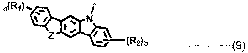


R1, R2, Z, a et b sont tels que définis selon la revendication 1. - Dispositif électroluminescent organique selon la revendication 1, dans lequel la formule 2 est représentée par l'une des formules 14 à 17 suivantes :


A1, A2, L1 et X1 à X16 sont tels que définis selon la revendication 1. - Dispositif électroluminescent organique selon la revendication 1, dans lequel, dans la formule 2,
A1 et A2 sont sélectionnés chacun indépendamment parmi le groupe constitué de phényle, biphényle, terphényle, naphtyle, fluorényle, benzofluorényle, phénanthrényle, anthracényle, indényle, triphénylényle, pyrényle, tétracényle, pérylényle, chrysényle et fluoranthényle. - Dispositif électroluminescent organique selon la revendication 1, dans lequel, dans la formule 2,
L1 représente l'une des formules 18 à 30 suivantes :





Xi à Xp représentent chacun indépendamment de l'hydrogène, du deutérium, un halogène, un cyano, un alkyle (C1-C30) substitué ou non substitué, un alcényle (C2-C30) substitué ou non substitué, un alcynyle (C2-C30) substitué ou non substitué, un cycloalkyle (C3-C30) substitué ou non substitué, un aryle (C6-C60) substitué ou non substitué, un hétéroaryle à 3 à 30 chaînons substitué ou non substitué, un trialkyl(C1-C30)silyle substitué ou non substitué, un triaryl(C6-C30)silyle substitué ou non substitué, un dialkyl(C1-C30)aryl(C6-C30)silyle substitué ou non substitué, ou un mono ou diaryl(C6-C30)amino substitué ou non substitué; ou des substituants adjacents peuvent être liés les uns aux autres pour former un cycle alicyclique ou aromatique (C3-C30), mono ou polycyclique, substitué ou non substitué, dont l'atome(les atomes) de carbone peut(peuvent) être remplacé(s) par au moins un hétéroatome sélectionné parmi azote, oxygène et soufre. - Dispositif électroluminescent organique selon la revendication 1, dans lequel dans les formules 1 et 2, les substituants de l'alkyle substitué, de l'alcényle substitué, de l'alcynyle substitué, de l'alcoxy substitué, du cycloalkyle substitué, du trialkylsilyle substitué, du dialkylarylsilyle substitué, de l'alkyldiarylsilyle substitué, du triarylsilyle substitué, du mono ou dialkylamino substitué, du mono ou diarylamino substitué, de l'alkylarylamino substitué, de l'aryl(ène) substitué, de l'hétéroaryle substitué et du cycle alicyclique ou aromatique (C3-C30) substitué, mono ou polycyclique dans R1 à R4, R7 et R8, L1 et X1 à X16 sont chacun indépendamment au moins l'un sélectionné parmi le groupe constitué de deutérium, d'un halogène, d'un cyano, d'un carboxyle, d'un nitro, d'un hydroxyle, d'un alkyle (C1-C30), d'un haloalkyle (C1-C30), d'un alcényle (C2-C30), d'un alcynyle (C2-C30), d'un alcoxy (C1-C30), d'un alkylthio (C1-C30), d'un cycloalkyle (C3-C30), d'un cycloalcényle (C3-C30), d'un hétérocycloalkyle à 3 à 7 chaînons, d'un aryloxy (C6-C30), d'un arylthio (C6-C30), d'un hétéroaryle à 3 à 30 chaînons non substitué ou substitué par un aryle (C6-C30), un aryle (C6-C30) non substitué ou substitué par un hétéroaryle à 3 à 30 chaînons, un trialkyl(C1-C30)silyle, un triaryl(C6-C30)silyle, un dialkyl(C1-C30)aryl(C6-C30)silyle, un alkyl(C1-C30)diaryl(C6-C30)silyle, un amino, un mono ou dialkyl(C1-C30)amino, un mono ou diaryl(C6-C30)amino, un alkyl(C1-C30)aryl(C6-C30)amino, un alkyl(C1-C30)carbonyle, un alcoxy(C1-C30)carbonyle, un aryl(C6-C30)carbonyle, un diaryl(C6-C30)boronyle, un dialkyl(C1-C30)boronyle, un alkyl(C1-C30)aryl(C6-C30)boronyle, un aryl(C6-C30)alkyle(C1-C30) et un alkyl(C1-C30)aryle (C6-C30).
- Dispositif électroluminescent organique selon la revendication 1, dans lequel le premier composé hôte représenté par la formule 1 est sélectionné parmi le groupe constitué de :





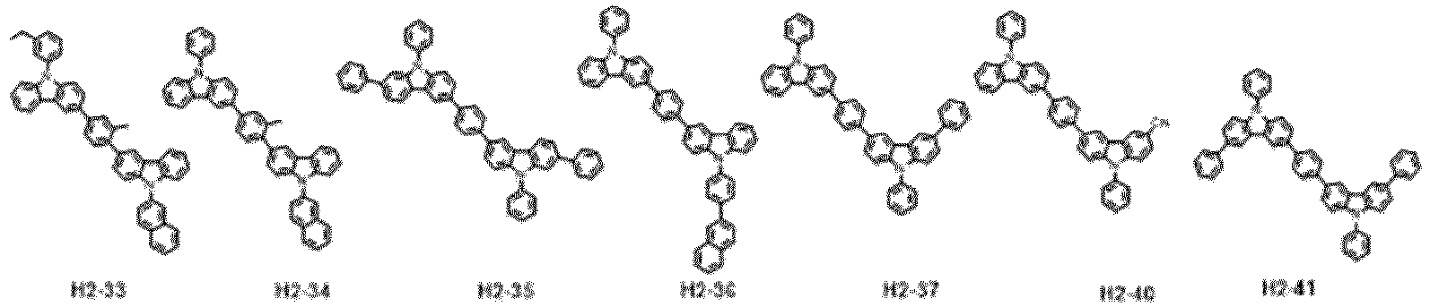
- Dispositif électroluminescent organique selon la revendication 1, dans lequel le deuxième composé hôte représenté par la formule 2, est sélectionné parmi le groupe constitué de :




Applications Claiming Priority (5)
| Application Number | Priority Date | Filing Date | Title |
|---|---|---|---|
| KR20150091223 | 2015-06-26 | ||
| KR1020160002171A KR20170001552A (ko) | 2015-06-26 | 2016-01-07 | 복수종의 호스트 재료와 이를 포함하는 유기 전계 발광 소자 |
| KR1020160048912A KR102646953B1 (ko) | 2015-06-26 | 2016-04-21 | 복수종의 호스트 재료와 이를 포함하는 유기 전계 발광 소자 |
| EP16814586.0A EP3313958B1 (fr) | 2015-06-26 | 2016-05-13 | Matériau hôte multicomposant et dispositif électroluminescent organique comprenant ce matériau |
| PCT/KR2016/005098 WO2016208873A1 (fr) | 2015-06-26 | 2016-05-13 | Matériau hôte multicomposant et dispositif électroluminescent organique comprenant ce matériau |
Related Parent Applications (2)
| Application Number | Title | Priority Date | Filing Date |
|---|---|---|---|
| EP16814586.0A Division EP3313958B1 (fr) | 2015-06-26 | 2016-05-13 | Matériau hôte multicomposant et dispositif électroluminescent organique comprenant ce matériau |
| EP16814586.0A Division-Into EP3313958B1 (fr) | 2015-06-26 | 2016-05-13 | Matériau hôte multicomposant et dispositif électroluminescent organique comprenant ce matériau |
Publications (2)
| Publication Number | Publication Date |
|---|---|
| EP3636726A1 EP3636726A1 (fr) | 2020-04-15 |
| EP3636726B1 true EP3636726B1 (fr) | 2021-07-14 |
Family
ID=57832083
Family Applications (2)
| Application Number | Title | Priority Date | Filing Date |
|---|---|---|---|
| EP19209591.7A Active EP3636726B1 (fr) | 2015-06-26 | 2016-05-13 | Matériau hôte multicomposant et dispositif électroluminescent organique comprenant ce matériau |
| EP16814586.0A Active EP3313958B1 (fr) | 2015-06-26 | 2016-05-13 | Matériau hôte multicomposant et dispositif électroluminescent organique comprenant ce matériau |
Family Applications After (1)
| Application Number | Title | Priority Date | Filing Date |
|---|---|---|---|
| EP16814586.0A Active EP3313958B1 (fr) | 2015-06-26 | 2016-05-13 | Matériau hôte multicomposant et dispositif électroluminescent organique comprenant ce matériau |
Country Status (6)
| Country | Link |
|---|---|
| US (3) | US20180301636A1 (fr) |
| EP (2) | EP3636726B1 (fr) |
| JP (1) | JP6735295B2 (fr) |
| KR (3) | KR20170001552A (fr) |
| CN (2) | CN113206210A (fr) |
| TW (1) | TWI699365B (fr) |
Families Citing this family (18)
| Publication number | Priority date | Publication date | Assignee | Title |
|---|---|---|---|---|
| KR20160136211A (ko) * | 2015-05-19 | 2016-11-29 | 롬엔드하스전자재료코리아유한회사 | 인광 호스트 재료 및 이를 포함하는 유기 전계 발광 소자 |
| CN109564973B (zh) | 2017-03-30 | 2023-03-31 | 株式会社Lg化学 | 有机发光器件 |
| KR102075251B1 (ko) | 2017-07-07 | 2020-02-07 | 주식회사 엘지화학 | 신규한 화합물 및 이를 포함하는 유기 발광 소자 |
| KR102171941B1 (ko) | 2017-09-22 | 2020-10-30 | 주식회사 엘지화학 | 신규한 화합물 및 이를 포함하는 유기 발광 소자 |
| KR102244800B1 (ko) | 2017-12-11 | 2021-04-26 | 주식회사 엘지화학 | 유기 발광 소자 및 이의 제조방법 |
| KR102849046B1 (ko) | 2018-03-16 | 2025-08-22 | 듀폰스페셜티머터리얼스코리아 유한회사 | 유기 전계 발광 소자용 복합 재료, 복수 종의 호스트 재료 및 이를 포함하는 유기 전계 발광 소자 |
| KR102550691B1 (ko) * | 2018-06-15 | 2023-07-04 | 삼성디스플레이 주식회사 | 헤테로시클릭 화합물 및 이를 포함한 유기 발광 소자 |
| KR102595520B1 (ko) * | 2018-07-05 | 2023-10-30 | 엘지디스플레이 주식회사 | 헤테로아릴기를 가진 벤즈아졸 유도체 및 이를 포함하는 유기전계발광소자 |
| KR102711310B1 (ko) * | 2018-10-02 | 2024-09-26 | 엘지디스플레이 주식회사 | 유기전계발광소자 |
| KR20200103524A (ko) * | 2019-02-25 | 2020-09-02 | 롬엔드하스전자재료코리아유한회사 | 유기 전계 발광 화합물 및 이를 포함하는 유기 전계 발광 소자 |
| US12227525B2 (en) * | 2019-08-14 | 2025-02-18 | Universal Display Corporation | Organic electroluminescent materials and devices |
| KR20210028825A (ko) * | 2019-09-05 | 2021-03-15 | 롬엔드하스전자재료코리아유한회사 | 유기 전계 발광 화합물 및 이를 포함하는 유기 전계 발광 소자 |
| KR102782649B1 (ko) * | 2019-10-02 | 2025-03-17 | 엘지디스플레이 주식회사 | 유기전계발광소자 |
| JP2021180307A (ja) * | 2020-05-13 | 2021-11-18 | ローム・アンド・ハース・エレクトロニック・マテリアルズ・コリア・リミテッド | 複数のホスト材料及びそれを含む有機エレクトロルミネッセントデバイス |
| KR102510700B1 (ko) * | 2021-03-31 | 2023-03-20 | 엘티소재주식회사 | 헤테로고리 화합물, 이를 포함하는 유기 발광 소자 및 유기물층용 조성물 |
| CN115466265A (zh) * | 2021-06-10 | 2022-12-13 | 罗门哈斯电子材料韩国有限公司 | 多种主体材料和包含其的有机电致发光装置 |
| CN114539270B (zh) * | 2021-12-09 | 2024-03-29 | 上海钥熠电子科技有限公司 | 含有咔唑衍生物的化合物及其在有机电致发光器件中的应用 |
| KR20250140875A (ko) | 2024-03-19 | 2025-09-26 | 주식회사 엘지에너지솔루션 | 시뮬레이션 장치 및 시뮬레이션 방법 |
Family Cites Families (20)
| Publication number | Priority date | Publication date | Assignee | Title |
|---|---|---|---|---|
| TWI471405B (zh) * | 2009-03-31 | 2015-02-01 | Nippon Steel & Sumikin Chem Co | A phosphorescent element material, and an organic electroluminescent device using the same |
| JP5124785B2 (ja) * | 2009-12-07 | 2013-01-23 | 新日鉄住金化学株式会社 | 有機発光材料及び有機発光素子 |
| TW201300501A (zh) * | 2010-07-30 | 2013-01-01 | 羅門哈斯電子材料韓國公司 | 使用電場發光化合物作為發光材料之電場發光裝置 |
| US9530969B2 (en) * | 2011-12-05 | 2016-12-27 | Idemitsu Kosan Co., Ltd. | Material for organic electroluminescence device and organic electroluminescence device |
| EP2790239B1 (fr) * | 2011-12-05 | 2020-02-05 | Idemitsu Kosan Co., Ltd | Matériau pour élément électroluminescent organique et élément électroluminescent organique |
| KR101986570B1 (ko) * | 2011-12-15 | 2019-06-07 | 닛테츠 케미컬 앤드 머티리얼 가부시키가이샤 | 유기 전계 발광 소자 |
| TWI585091B (zh) * | 2012-03-30 | 2017-06-01 | 新日鐵住金化學股份有限公司 | Organic electroluminescent elements |
| WO2013168688A1 (fr) * | 2012-05-10 | 2013-11-14 | コニカミノルタ株式会社 | Élément à électroluminescence organique, dispositif d'éclairage et dispositif d'affichage |
| KR20140032823A (ko) * | 2012-09-07 | 2014-03-17 | 롬엔드하스전자재료코리아유한회사 | 유기 전계 발광 소자 |
| WO2014097813A1 (fr) * | 2012-12-17 | 2014-06-26 | 新日鉄住金化学株式会社 | Élément électroluminescent à champ électrique organique |
| KR101820865B1 (ko) * | 2013-01-17 | 2018-01-22 | 삼성전자주식회사 | 유기광전자소자용 재료, 이를 포함하는 유기발광소자 및 상기 유기발광소자를 포함하는 표시장치 |
| EP2821459B1 (fr) | 2013-07-01 | 2017-10-04 | Cheil Industries Inc. | Composition et dispositif optoélectronique organique et dispositif d'affichage |
| JP6381874B2 (ja) * | 2013-07-18 | 2018-08-29 | 三星ディスプレイ株式會社Samsung Display Co.,Ltd. | 有機エレクトロルミネッセンス素子用材料及びそれを用いた有機エレクトロルミネッセンス素子 |
| KR102158000B1 (ko) * | 2013-09-26 | 2020-09-22 | 롬엔드하스전자재료코리아유한회사 | 유기 전계 발광 소자 |
| KR101802861B1 (ko) * | 2014-02-14 | 2017-11-30 | 삼성디스플레이 주식회사 | 유기 발광 소자 |
| WO2015156587A1 (fr) * | 2014-04-08 | 2015-10-15 | Rohm And Haas Electronic Materials Korea Ltd. | Matériau hôte à plusieurs composants et dispositif électroluminescent organique le comprenant |
| KR101754715B1 (ko) * | 2014-04-08 | 2017-07-10 | 롬엔드하스전자재료코리아유한회사 | 복수종의 호스트 재료와 이를 포함하는 유기 전계 발광 소자 |
| KR101502316B1 (ko) | 2014-04-18 | 2015-03-13 | 롬엔드하스전자재료코리아유한회사 | 복수종의 호스트 재료 및 이를 포함하는 유기 전계 발광 소자 |
| KR102244071B1 (ko) * | 2014-05-02 | 2021-04-26 | 삼성디스플레이 주식회사 | 유기 발광 소자 |
| KR102273047B1 (ko) * | 2014-06-30 | 2021-07-06 | 삼성디스플레이 주식회사 | 유기 발광 소자 |
-
2016
- 2016-01-07 KR KR1020160002171A patent/KR20170001552A/ko active Pending
- 2016-04-21 KR KR1020160048912A patent/KR102646953B1/ko active Active
- 2016-05-13 EP EP19209591.7A patent/EP3636726B1/fr active Active
- 2016-05-13 US US15/580,082 patent/US20180301636A1/en not_active Abandoned
- 2016-05-13 EP EP16814586.0A patent/EP3313958B1/fr active Active
- 2016-05-13 CN CN202110494913.3A patent/CN113206210A/zh active Pending
- 2016-05-13 JP JP2017563341A patent/JP6735295B2/ja active Active
- 2016-05-13 CN CN201680034175.1A patent/CN107771206B/zh active Active
- 2016-06-07 TW TW105118037A patent/TWI699365B/zh active
-
2021
- 2021-03-18 US US17/205,211 patent/US20210210699A1/en not_active Abandoned
-
2023
- 2023-11-15 US US18/509,819 patent/US20240099132A1/en active Pending
-
2024
- 2024-03-07 KR KR1020240032489A patent/KR102849709B1/ko active Active
Also Published As
| Publication number | Publication date |
|---|---|
| CN107771206A (zh) | 2018-03-06 |
| TWI699365B (zh) | 2020-07-21 |
| US20210210699A1 (en) | 2021-07-08 |
| CN107771206B (zh) | 2021-05-28 |
| KR20170001563A (ko) | 2017-01-04 |
| KR102849709B1 (ko) | 2025-08-27 |
| EP3636726A1 (fr) | 2020-04-15 |
| EP3313958A4 (fr) | 2019-02-27 |
| EP3313958A1 (fr) | 2018-05-02 |
| KR102646953B1 (ko) | 2024-03-14 |
| KR20240037908A (ko) | 2024-03-22 |
| CN113206210A (zh) | 2021-08-03 |
| TW201700479A (zh) | 2017-01-01 |
| US20180301636A1 (en) | 2018-10-18 |
| JP2018520513A (ja) | 2018-07-26 |
| US20240099132A1 (en) | 2024-03-21 |
| EP3313958B1 (fr) | 2020-02-12 |
| KR20170001552A (ko) | 2017-01-04 |
| JP6735295B2 (ja) | 2020-08-05 |
Similar Documents
| Publication | Publication Date | Title |
|---|---|---|
| US12457899B2 (en) | Multi-component host material and an organic electroluminescence device comprising the same | |
| KR102849709B1 (ko) | 복수종의 호스트 재료와 이를 포함하는 유기 전계 발광 소자 | |
| KR102660550B1 (ko) | 복수종의 호스트 재료 및 이를 포함하는 유기 전계 발광 소자 | |
| EP3183234B1 (fr) | Pluralité de matériaux hôtes et dispositif électroluminescent organique comprenant ces matériaux | |
| EP3170206B1 (fr) | Dispositif électroluminescent organique | |
| KR102332629B1 (ko) | 복수종의 호스트 재료와 이를 포함하는 유기 전계 발광 소자 | |
| EP3322693B1 (fr) | Pluralité de matériaux hôtes et dispositif électroluminescent organique comprenant ces matériaux | |
| KR102502306B1 (ko) | 유기 전계 발광 소자 | |
| EP3268449B1 (fr) | Pluralité de matériaux hôtes et dispositif électroluminescent organique comprenant ces matériaux | |
| KR102357467B1 (ko) | 유기 전계 발광 소자 | |
| KR102395933B1 (ko) | 복수종의 호스트 재료와 이를 포함하는 유기 전계 발광 소자 | |
| KR20240026971A (ko) | 복수종의 호스트 재료 및 이를 포함하는 유기 전계 발광 소자 | |
| KR102593644B1 (ko) | 복수종의 호스트 재료 및 이를 포함하는 유기 전계 발광 소자 | |
| KR20250128287A (ko) | 복수종의 호스트 재료와 이를 포함하는 유기 전계 발광 소자 | |
| KR20230028739A (ko) | 복수종의 호스트 재료 및 이를 포함하는 유기 전계 발광 소자 | |
| KR102520279B1 (ko) | 유기 전계 발광 소자 | |
| KR102409002B1 (ko) | 복수종의 호스트 재료 및 이를 포함하는 유기 전계 발광 소자 | |
| KR102744947B1 (ko) | 복수 종의 호스트 재료 및 이를 포함하는 유기 전계 발광 소자 | |
| CN118834156A (zh) | 多种主体材料和包含其的有机电致发光装置 |
Legal Events
| Date | Code | Title | Description |
|---|---|---|---|
| PUAI | Public reference made under article 153(3) epc to a published international application that has entered the european phase |
Free format text: ORIGINAL CODE: 0009012 |
|
| STAA | Information on the status of an ep patent application or granted ep patent |
Free format text: STATUS: REQUEST FOR EXAMINATION WAS MADE |
|
| 17P | Request for examination filed |
Effective date: 20191115 |
|
| AC | Divisional application: reference to earlier application |
Ref document number: 3313958 Country of ref document: EP Kind code of ref document: P |
|
| AK | Designated contracting states |
Kind code of ref document: A1 Designated state(s): AL AT BE BG CH CY CZ DE DK EE ES FI FR GB GR HR HU IE IS IT LI LT LU LV MC MK MT NL NO PL PT RO RS SE SI SK SM TR |
|
| GRAP | Despatch of communication of intention to grant a patent |
Free format text: ORIGINAL CODE: EPIDOSNIGR1 |
|
| STAA | Information on the status of an ep patent application or granted ep patent |
Free format text: STATUS: GRANT OF PATENT IS INTENDED |
|
| INTG | Intention to grant announced |
Effective date: 20210305 |
|
| GRAS | Grant fee paid |
Free format text: ORIGINAL CODE: EPIDOSNIGR3 |
|
| GRAA | (expected) grant |
Free format text: ORIGINAL CODE: 0009210 |
|
| STAA | Information on the status of an ep patent application or granted ep patent |
Free format text: STATUS: THE PATENT HAS BEEN GRANTED |
|
| AC | Divisional application: reference to earlier application |
Ref document number: 3313958 Country of ref document: EP Kind code of ref document: P |
|
| AK | Designated contracting states |
Kind code of ref document: B1 Designated state(s): AL AT BE BG CH CY CZ DE DK EE ES FI FR GB GR HR HU IE IS IT LI LT LU LV MC MK MT NL NO PL PT RO RS SE SI SK SM TR |
|
| REG | Reference to a national code |
Ref country code: GB Ref legal event code: FG4D |
|
| REG | Reference to a national code |
Ref country code: DE Ref legal event code: R096 Ref document number: 602016060808 Country of ref document: DE |
|
| REG | Reference to a national code |
Ref country code: IE Ref legal event code: FG4D |
|
| REG | Reference to a national code |
Ref country code: AT Ref legal event code: REF Ref document number: 1410657 Country of ref document: AT Kind code of ref document: T Effective date: 20210815 |
|
| REG | Reference to a national code |
Ref country code: LT Ref legal event code: MG9D |
|
| REG | Reference to a national code |
Ref country code: NL Ref legal event code: MP Effective date: 20210714 |
|
| REG | Reference to a national code |
Ref country code: AT Ref legal event code: MK05 Ref document number: 1410657 Country of ref document: AT Kind code of ref document: T Effective date: 20210714 |
|
| PG25 | Lapsed in a contracting state [announced via postgrant information from national office to epo] |
Ref country code: ES Free format text: LAPSE BECAUSE OF FAILURE TO SUBMIT A TRANSLATION OF THE DESCRIPTION OR TO PAY THE FEE WITHIN THE PRESCRIBED TIME-LIMIT Effective date: 20210714 Ref country code: RS Free format text: LAPSE BECAUSE OF FAILURE TO SUBMIT A TRANSLATION OF THE DESCRIPTION OR TO PAY THE FEE WITHIN THE PRESCRIBED TIME-LIMIT Effective date: 20210714 Ref country code: SE Free format text: LAPSE BECAUSE OF FAILURE TO SUBMIT A TRANSLATION OF THE DESCRIPTION OR TO PAY THE FEE WITHIN THE PRESCRIBED TIME-LIMIT Effective date: 20210714 Ref country code: AT Free format text: LAPSE BECAUSE OF FAILURE TO SUBMIT A TRANSLATION OF THE DESCRIPTION OR TO PAY THE FEE WITHIN THE PRESCRIBED TIME-LIMIT Effective date: 20210714 Ref country code: BG Free format text: LAPSE BECAUSE OF FAILURE TO SUBMIT A TRANSLATION OF THE DESCRIPTION OR TO PAY THE FEE WITHIN THE PRESCRIBED TIME-LIMIT Effective date: 20211014 Ref country code: LT Free format text: LAPSE BECAUSE OF FAILURE TO SUBMIT A TRANSLATION OF THE DESCRIPTION OR TO PAY THE FEE WITHIN THE PRESCRIBED TIME-LIMIT Effective date: 20210714 Ref country code: NO Free format text: LAPSE BECAUSE OF FAILURE TO SUBMIT A TRANSLATION OF THE DESCRIPTION OR TO PAY THE FEE WITHIN THE PRESCRIBED TIME-LIMIT Effective date: 20211014 Ref country code: PT Free format text: LAPSE BECAUSE OF FAILURE TO SUBMIT A TRANSLATION OF THE DESCRIPTION OR TO PAY THE FEE WITHIN THE PRESCRIBED TIME-LIMIT Effective date: 20211115 Ref country code: NL Free format text: LAPSE BECAUSE OF FAILURE TO SUBMIT A TRANSLATION OF THE DESCRIPTION OR TO PAY THE FEE WITHIN THE PRESCRIBED TIME-LIMIT Effective date: 20210714 Ref country code: FI Free format text: LAPSE BECAUSE OF FAILURE TO SUBMIT A TRANSLATION OF THE DESCRIPTION OR TO PAY THE FEE WITHIN THE PRESCRIBED TIME-LIMIT Effective date: 20210714 Ref country code: HR Free format text: LAPSE BECAUSE OF FAILURE TO SUBMIT A TRANSLATION OF THE DESCRIPTION OR TO PAY THE FEE WITHIN THE PRESCRIBED TIME-LIMIT Effective date: 20210714 |
|
| PG25 | Lapsed in a contracting state [announced via postgrant information from national office to epo] |
Ref country code: PL Free format text: LAPSE BECAUSE OF FAILURE TO SUBMIT A TRANSLATION OF THE DESCRIPTION OR TO PAY THE FEE WITHIN THE PRESCRIBED TIME-LIMIT Effective date: 20210714 Ref country code: LV Free format text: LAPSE BECAUSE OF FAILURE TO SUBMIT A TRANSLATION OF THE DESCRIPTION OR TO PAY THE FEE WITHIN THE PRESCRIBED TIME-LIMIT Effective date: 20210714 Ref country code: GR Free format text: LAPSE BECAUSE OF FAILURE TO SUBMIT A TRANSLATION OF THE DESCRIPTION OR TO PAY THE FEE WITHIN THE PRESCRIBED TIME-LIMIT Effective date: 20211015 |
|
| REG | Reference to a national code |
Ref country code: DE Ref legal event code: R097 Ref document number: 602016060808 Country of ref document: DE |
|
| PG25 | Lapsed in a contracting state [announced via postgrant information from national office to epo] |
Ref country code: DK Free format text: LAPSE BECAUSE OF FAILURE TO SUBMIT A TRANSLATION OF THE DESCRIPTION OR TO PAY THE FEE WITHIN THE PRESCRIBED TIME-LIMIT Effective date: 20210714 |
|
| PLBE | No opposition filed within time limit |
Free format text: ORIGINAL CODE: 0009261 |
|
| STAA | Information on the status of an ep patent application or granted ep patent |
Free format text: STATUS: NO OPPOSITION FILED WITHIN TIME LIMIT |
|
| PG25 | Lapsed in a contracting state [announced via postgrant information from national office to epo] |
Ref country code: SM Free format text: LAPSE BECAUSE OF FAILURE TO SUBMIT A TRANSLATION OF THE DESCRIPTION OR TO PAY THE FEE WITHIN THE PRESCRIBED TIME-LIMIT Effective date: 20210714 Ref country code: SK Free format text: LAPSE BECAUSE OF FAILURE TO SUBMIT A TRANSLATION OF THE DESCRIPTION OR TO PAY THE FEE WITHIN THE PRESCRIBED TIME-LIMIT Effective date: 20210714 Ref country code: RO Free format text: LAPSE BECAUSE OF FAILURE TO SUBMIT A TRANSLATION OF THE DESCRIPTION OR TO PAY THE FEE WITHIN THE PRESCRIBED TIME-LIMIT Effective date: 20210714 Ref country code: EE Free format text: LAPSE BECAUSE OF FAILURE TO SUBMIT A TRANSLATION OF THE DESCRIPTION OR TO PAY THE FEE WITHIN THE PRESCRIBED TIME-LIMIT Effective date: 20210714 Ref country code: CZ Free format text: LAPSE BECAUSE OF FAILURE TO SUBMIT A TRANSLATION OF THE DESCRIPTION OR TO PAY THE FEE WITHIN THE PRESCRIBED TIME-LIMIT Effective date: 20210714 Ref country code: AL Free format text: LAPSE BECAUSE OF FAILURE TO SUBMIT A TRANSLATION OF THE DESCRIPTION OR TO PAY THE FEE WITHIN THE PRESCRIBED TIME-LIMIT Effective date: 20210714 |
|
| 26N | No opposition filed |
Effective date: 20220419 |
|
| PG25 | Lapsed in a contracting state [announced via postgrant information from national office to epo] |
Ref country code: IT Free format text: LAPSE BECAUSE OF FAILURE TO SUBMIT A TRANSLATION OF THE DESCRIPTION OR TO PAY THE FEE WITHIN THE PRESCRIBED TIME-LIMIT Effective date: 20210714 |
|
| REG | Reference to a national code |
Ref country code: CH Ref legal event code: PL |
|
| REG | Reference to a national code |
Ref country code: BE Ref legal event code: MM Effective date: 20220531 |
|
| GBPC | Gb: european patent ceased through non-payment of renewal fee |
Effective date: 20220513 |
|
| PG25 | Lapsed in a contracting state [announced via postgrant information from national office to epo] |
Ref country code: MC Free format text: LAPSE BECAUSE OF FAILURE TO SUBMIT A TRANSLATION OF THE DESCRIPTION OR TO PAY THE FEE WITHIN THE PRESCRIBED TIME-LIMIT Effective date: 20210714 Ref country code: LU Free format text: LAPSE BECAUSE OF NON-PAYMENT OF DUE FEES Effective date: 20220513 Ref country code: LI Free format text: LAPSE BECAUSE OF NON-PAYMENT OF DUE FEES Effective date: 20220531 Ref country code: CH Free format text: LAPSE BECAUSE OF NON-PAYMENT OF DUE FEES Effective date: 20220531 |
|
| PG25 | Lapsed in a contracting state [announced via postgrant information from national office to epo] |
Ref country code: IE Free format text: LAPSE BECAUSE OF NON-PAYMENT OF DUE FEES Effective date: 20220513 Ref country code: FR Free format text: LAPSE BECAUSE OF NON-PAYMENT OF DUE FEES Effective date: 20220531 |
|
| PG25 | Lapsed in a contracting state [announced via postgrant information from national office to epo] |
Ref country code: GB Free format text: LAPSE BECAUSE OF NON-PAYMENT OF DUE FEES Effective date: 20220513 Ref country code: BE Free format text: LAPSE BECAUSE OF NON-PAYMENT OF DUE FEES Effective date: 20220531 |
|
| P01 | Opt-out of the competence of the unified patent court (upc) registered |
Effective date: 20230530 |
|
| PG25 | Lapsed in a contracting state [announced via postgrant information from national office to epo] |
Ref country code: MK Free format text: LAPSE BECAUSE OF FAILURE TO SUBMIT A TRANSLATION OF THE DESCRIPTION OR TO PAY THE FEE WITHIN THE PRESCRIBED TIME-LIMIT Effective date: 20210714 Ref country code: CY Free format text: LAPSE BECAUSE OF FAILURE TO SUBMIT A TRANSLATION OF THE DESCRIPTION OR TO PAY THE FEE WITHIN THE PRESCRIBED TIME-LIMIT Effective date: 20210714 |
|
| PG25 | Lapsed in a contracting state [announced via postgrant information from national office to epo] |
Ref country code: HU Free format text: LAPSE BECAUSE OF FAILURE TO SUBMIT A TRANSLATION OF THE DESCRIPTION OR TO PAY THE FEE WITHIN THE PRESCRIBED TIME-LIMIT; INVALID AB INITIO Effective date: 20160513 |
|
| PG25 | Lapsed in a contracting state [announced via postgrant information from national office to epo] |
Ref country code: MT Free format text: LAPSE BECAUSE OF FAILURE TO SUBMIT A TRANSLATION OF THE DESCRIPTION OR TO PAY THE FEE WITHIN THE PRESCRIBED TIME-LIMIT Effective date: 20210714 |
|
| REG | Reference to a national code |
Ref country code: DE Ref legal event code: R081 Ref document number: 602016060808 Country of ref document: DE Owner name: DUPONT SPECIALTY MATERIALS KOREA LTD., CHEONAN, KR Free format text: FORMER OWNER: ROHM AND HAAS ELECTRONIC MATERIALS KOREA LTD., CHEONAN-SI, CHUNGCHEONGNAM-DO, KR |
|
| PGFP | Annual fee paid to national office [announced via postgrant information from national office to epo] |
Ref country code: DE Payment date: 20250402 Year of fee payment: 10 |
|
| PG25 | Lapsed in a contracting state [announced via postgrant information from national office to epo] |
Ref country code: TR Free format text: LAPSE BECAUSE OF FAILURE TO SUBMIT A TRANSLATION OF THE DESCRIPTION OR TO PAY THE FEE WITHIN THE PRESCRIBED TIME-LIMIT Effective date: 20210714 |