EP3636799B1 - Beschichtungsverfahren für rohrartige perc-solarzellen - Google Patents
Beschichtungsverfahren für rohrartige perc-solarzellen Download PDFInfo
- Publication number
- EP3636799B1 EP3636799B1 EP17912428.4A EP17912428A EP3636799B1 EP 3636799 B1 EP3636799 B1 EP 3636799B1 EP 17912428 A EP17912428 A EP 17912428A EP 3636799 B1 EP3636799 B1 EP 3636799B1
- Authority
- EP
- European Patent Office
- Prior art keywords
- graphite boat
- flow rate
- silane
- film
- coating
- Prior art date
- Legal status (The legal status is an assumption and is not a legal conclusion. Google has not performed a legal analysis and makes no representation as to the accuracy of the status listed.)
- Active
Links
Images
Classifications
-
- C—CHEMISTRY; METALLURGY
- C23—COATING METALLIC MATERIAL; COATING MATERIAL WITH METALLIC MATERIAL; CHEMICAL SURFACE TREATMENT; DIFFUSION TREATMENT OF METALLIC MATERIAL; COATING BY VACUUM EVAPORATION, BY SPUTTERING, BY ION IMPLANTATION OR BY CHEMICAL VAPOUR DEPOSITION, IN GENERAL; INHIBITING CORROSION OF METALLIC MATERIAL OR INCRUSTATION IN GENERAL
- C23C—COATING METALLIC MATERIAL; COATING MATERIAL WITH METALLIC MATERIAL; SURFACE TREATMENT OF METALLIC MATERIAL BY DIFFUSION INTO THE SURFACE, BY CHEMICAL CONVERSION OR SUBSTITUTION; COATING BY VACUUM EVAPORATION, BY SPUTTERING, BY ION IMPLANTATION OR BY CHEMICAL VAPOUR DEPOSITION, IN GENERAL
- C23C16/00—Chemical coating by decomposition of gaseous compounds, without leaving reaction products of surface material in the coating, i.e. chemical vapour deposition [CVD] processes
- C23C16/44—Chemical coating by decomposition of gaseous compounds, without leaving reaction products of surface material in the coating, i.e. chemical vapour deposition [CVD] processes characterised by the method of coating
- C23C16/458—Chemical coating by decomposition of gaseous compounds, without leaving reaction products of surface material in the coating, i.e. chemical vapour deposition [CVD] processes characterised by the method of coating characterised by the method used for supporting substrates in the reaction chamber
- C23C16/4581—Chemical coating by decomposition of gaseous compounds, without leaving reaction products of surface material in the coating, i.e. chemical vapour deposition [CVD] processes characterised by the method of coating characterised by the method used for supporting substrates in the reaction chamber characterised by material of construction or surface finish of the means for supporting the substrate
-
- H—ELECTRICITY
- H10—SEMICONDUCTOR DEVICES; ELECTRIC SOLID-STATE DEVICES NOT OTHERWISE PROVIDED FOR
- H10F—INORGANIC SEMICONDUCTOR DEVICES SENSITIVE TO INFRARED RADIATION, LIGHT, ELECTROMAGNETIC RADIATION OF SHORTER WAVELENGTH OR CORPUSCULAR RADIATION
- H10F77/00—Constructional details of devices covered by this subclass
- H10F77/30—Coatings
- H10F77/306—Coatings for devices having potential barriers
- H10F77/311—Coatings for devices having potential barriers for photovoltaic cells
-
- C—CHEMISTRY; METALLURGY
- C23—COATING METALLIC MATERIAL; COATING MATERIAL WITH METALLIC MATERIAL; CHEMICAL SURFACE TREATMENT; DIFFUSION TREATMENT OF METALLIC MATERIAL; COATING BY VACUUM EVAPORATION, BY SPUTTERING, BY ION IMPLANTATION OR BY CHEMICAL VAPOUR DEPOSITION, IN GENERAL; INHIBITING CORROSION OF METALLIC MATERIAL OR INCRUSTATION IN GENERAL
- C23C—COATING METALLIC MATERIAL; COATING MATERIAL WITH METALLIC MATERIAL; SURFACE TREATMENT OF METALLIC MATERIAL BY DIFFUSION INTO THE SURFACE, BY CHEMICAL CONVERSION OR SUBSTITUTION; COATING BY VACUUM EVAPORATION, BY SPUTTERING, BY ION IMPLANTATION OR BY CHEMICAL VAPOUR DEPOSITION, IN GENERAL
- C23C16/00—Chemical coating by decomposition of gaseous compounds, without leaving reaction products of surface material in the coating, i.e. chemical vapour deposition [CVD] processes
- C23C16/44—Chemical coating by decomposition of gaseous compounds, without leaving reaction products of surface material in the coating, i.e. chemical vapour deposition [CVD] processes characterised by the method of coating
- C23C16/458—Chemical coating by decomposition of gaseous compounds, without leaving reaction products of surface material in the coating, i.e. chemical vapour deposition [CVD] processes characterised by the method of coating characterised by the method used for supporting substrates in the reaction chamber
-
- C—CHEMISTRY; METALLURGY
- C23—COATING METALLIC MATERIAL; COATING MATERIAL WITH METALLIC MATERIAL; CHEMICAL SURFACE TREATMENT; DIFFUSION TREATMENT OF METALLIC MATERIAL; COATING BY VACUUM EVAPORATION, BY SPUTTERING, BY ION IMPLANTATION OR BY CHEMICAL VAPOUR DEPOSITION, IN GENERAL; INHIBITING CORROSION OF METALLIC MATERIAL OR INCRUSTATION IN GENERAL
- C23C—COATING METALLIC MATERIAL; COATING MATERIAL WITH METALLIC MATERIAL; SURFACE TREATMENT OF METALLIC MATERIAL BY DIFFUSION INTO THE SURFACE, BY CHEMICAL CONVERSION OR SUBSTITUTION; COATING BY VACUUM EVAPORATION, BY SPUTTERING, BY ION IMPLANTATION OR BY CHEMICAL VAPOUR DEPOSITION, IN GENERAL
- C23C16/00—Chemical coating by decomposition of gaseous compounds, without leaving reaction products of surface material in the coating, i.e. chemical vapour deposition [CVD] processes
- C23C16/02—Pretreatment of the material to be coated
- C23C16/0209—Pretreatment of the material to be coated by heating
-
- C—CHEMISTRY; METALLURGY
- C23—COATING METALLIC MATERIAL; COATING MATERIAL WITH METALLIC MATERIAL; CHEMICAL SURFACE TREATMENT; DIFFUSION TREATMENT OF METALLIC MATERIAL; COATING BY VACUUM EVAPORATION, BY SPUTTERING, BY ION IMPLANTATION OR BY CHEMICAL VAPOUR DEPOSITION, IN GENERAL; INHIBITING CORROSION OF METALLIC MATERIAL OR INCRUSTATION IN GENERAL
- C23C—COATING METALLIC MATERIAL; COATING MATERIAL WITH METALLIC MATERIAL; SURFACE TREATMENT OF METALLIC MATERIAL BY DIFFUSION INTO THE SURFACE, BY CHEMICAL CONVERSION OR SUBSTITUTION; COATING BY VACUUM EVAPORATION, BY SPUTTERING, BY ION IMPLANTATION OR BY CHEMICAL VAPOUR DEPOSITION, IN GENERAL
- C23C16/00—Chemical coating by decomposition of gaseous compounds, without leaving reaction products of surface material in the coating, i.e. chemical vapour deposition [CVD] processes
- C23C16/22—Chemical coating by decomposition of gaseous compounds, without leaving reaction products of surface material in the coating, i.e. chemical vapour deposition [CVD] processes characterised by the deposition of inorganic material, other than metallic material
- C23C16/30—Deposition of compounds, mixtures or solid solutions, e.g. borides, carbides, nitrides
- C23C16/308—Oxynitrides
-
- C—CHEMISTRY; METALLURGY
- C23—COATING METALLIC MATERIAL; COATING MATERIAL WITH METALLIC MATERIAL; CHEMICAL SURFACE TREATMENT; DIFFUSION TREATMENT OF METALLIC MATERIAL; COATING BY VACUUM EVAPORATION, BY SPUTTERING, BY ION IMPLANTATION OR BY CHEMICAL VAPOUR DEPOSITION, IN GENERAL; INHIBITING CORROSION OF METALLIC MATERIAL OR INCRUSTATION IN GENERAL
- C23C—COATING METALLIC MATERIAL; COATING MATERIAL WITH METALLIC MATERIAL; SURFACE TREATMENT OF METALLIC MATERIAL BY DIFFUSION INTO THE SURFACE, BY CHEMICAL CONVERSION OR SUBSTITUTION; COATING BY VACUUM EVAPORATION, BY SPUTTERING, BY ION IMPLANTATION OR BY CHEMICAL VAPOUR DEPOSITION, IN GENERAL
- C23C16/00—Chemical coating by decomposition of gaseous compounds, without leaving reaction products of surface material in the coating, i.e. chemical vapour deposition [CVD] processes
- C23C16/22—Chemical coating by decomposition of gaseous compounds, without leaving reaction products of surface material in the coating, i.e. chemical vapour deposition [CVD] processes characterised by the deposition of inorganic material, other than metallic material
- C23C16/30—Deposition of compounds, mixtures or solid solutions, e.g. borides, carbides, nitrides
- C23C16/32—Carbides
- C23C16/325—Silicon carbide
-
- C—CHEMISTRY; METALLURGY
- C23—COATING METALLIC MATERIAL; COATING MATERIAL WITH METALLIC MATERIAL; CHEMICAL SURFACE TREATMENT; DIFFUSION TREATMENT OF METALLIC MATERIAL; COATING BY VACUUM EVAPORATION, BY SPUTTERING, BY ION IMPLANTATION OR BY CHEMICAL VAPOUR DEPOSITION, IN GENERAL; INHIBITING CORROSION OF METALLIC MATERIAL OR INCRUSTATION IN GENERAL
- C23C—COATING METALLIC MATERIAL; COATING MATERIAL WITH METALLIC MATERIAL; SURFACE TREATMENT OF METALLIC MATERIAL BY DIFFUSION INTO THE SURFACE, BY CHEMICAL CONVERSION OR SUBSTITUTION; COATING BY VACUUM EVAPORATION, BY SPUTTERING, BY ION IMPLANTATION OR BY CHEMICAL VAPOUR DEPOSITION, IN GENERAL
- C23C16/00—Chemical coating by decomposition of gaseous compounds, without leaving reaction products of surface material in the coating, i.e. chemical vapour deposition [CVD] processes
- C23C16/22—Chemical coating by decomposition of gaseous compounds, without leaving reaction products of surface material in the coating, i.e. chemical vapour deposition [CVD] processes characterised by the deposition of inorganic material, other than metallic material
- C23C16/30—Deposition of compounds, mixtures or solid solutions, e.g. borides, carbides, nitrides
- C23C16/34—Nitrides
- C23C16/345—Silicon nitride
-
- C—CHEMISTRY; METALLURGY
- C23—COATING METALLIC MATERIAL; COATING MATERIAL WITH METALLIC MATERIAL; CHEMICAL SURFACE TREATMENT; DIFFUSION TREATMENT OF METALLIC MATERIAL; COATING BY VACUUM EVAPORATION, BY SPUTTERING, BY ION IMPLANTATION OR BY CHEMICAL VAPOUR DEPOSITION, IN GENERAL; INHIBITING CORROSION OF METALLIC MATERIAL OR INCRUSTATION IN GENERAL
- C23C—COATING METALLIC MATERIAL; COATING MATERIAL WITH METALLIC MATERIAL; SURFACE TREATMENT OF METALLIC MATERIAL BY DIFFUSION INTO THE SURFACE, BY CHEMICAL CONVERSION OR SUBSTITUTION; COATING BY VACUUM EVAPORATION, BY SPUTTERING, BY ION IMPLANTATION OR BY CHEMICAL VAPOUR DEPOSITION, IN GENERAL
- C23C16/00—Chemical coating by decomposition of gaseous compounds, without leaving reaction products of surface material in the coating, i.e. chemical vapour deposition [CVD] processes
- C23C16/22—Chemical coating by decomposition of gaseous compounds, without leaving reaction products of surface material in the coating, i.e. chemical vapour deposition [CVD] processes characterised by the deposition of inorganic material, other than metallic material
- C23C16/30—Deposition of compounds, mixtures or solid solutions, e.g. borides, carbides, nitrides
- C23C16/40—Oxides
- C23C16/401—Oxides containing silicon
- C23C16/402—Silicon dioxide
-
- C—CHEMISTRY; METALLURGY
- C23—COATING METALLIC MATERIAL; COATING MATERIAL WITH METALLIC MATERIAL; CHEMICAL SURFACE TREATMENT; DIFFUSION TREATMENT OF METALLIC MATERIAL; COATING BY VACUUM EVAPORATION, BY SPUTTERING, BY ION IMPLANTATION OR BY CHEMICAL VAPOUR DEPOSITION, IN GENERAL; INHIBITING CORROSION OF METALLIC MATERIAL OR INCRUSTATION IN GENERAL
- C23C—COATING METALLIC MATERIAL; COATING MATERIAL WITH METALLIC MATERIAL; SURFACE TREATMENT OF METALLIC MATERIAL BY DIFFUSION INTO THE SURFACE, BY CHEMICAL CONVERSION OR SUBSTITUTION; COATING BY VACUUM EVAPORATION, BY SPUTTERING, BY ION IMPLANTATION OR BY CHEMICAL VAPOUR DEPOSITION, IN GENERAL
- C23C16/00—Chemical coating by decomposition of gaseous compounds, without leaving reaction products of surface material in the coating, i.e. chemical vapour deposition [CVD] processes
- C23C16/22—Chemical coating by decomposition of gaseous compounds, without leaving reaction products of surface material in the coating, i.e. chemical vapour deposition [CVD] processes characterised by the deposition of inorganic material, other than metallic material
- C23C16/30—Deposition of compounds, mixtures or solid solutions, e.g. borides, carbides, nitrides
- C23C16/40—Oxides
- C23C16/403—Oxides of aluminium, magnesium or beryllium
-
- C—CHEMISTRY; METALLURGY
- C23—COATING METALLIC MATERIAL; COATING MATERIAL WITH METALLIC MATERIAL; CHEMICAL SURFACE TREATMENT; DIFFUSION TREATMENT OF METALLIC MATERIAL; COATING BY VACUUM EVAPORATION, BY SPUTTERING, BY ION IMPLANTATION OR BY CHEMICAL VAPOUR DEPOSITION, IN GENERAL; INHIBITING CORROSION OF METALLIC MATERIAL OR INCRUSTATION IN GENERAL
- C23C—COATING METALLIC MATERIAL; COATING MATERIAL WITH METALLIC MATERIAL; SURFACE TREATMENT OF METALLIC MATERIAL BY DIFFUSION INTO THE SURFACE, BY CHEMICAL CONVERSION OR SUBSTITUTION; COATING BY VACUUM EVAPORATION, BY SPUTTERING, BY ION IMPLANTATION OR BY CHEMICAL VAPOUR DEPOSITION, IN GENERAL
- C23C16/00—Chemical coating by decomposition of gaseous compounds, without leaving reaction products of surface material in the coating, i.e. chemical vapour deposition [CVD] processes
- C23C16/44—Chemical coating by decomposition of gaseous compounds, without leaving reaction products of surface material in the coating, i.e. chemical vapour deposition [CVD] processes characterised by the method of coating
- C23C16/4401—Means for minimising impurities, e.g. dust, moisture or residual gas, in the reaction chamber
- C23C16/4404—Coatings or surface treatment on the inside of the reaction chamber or on parts thereof
-
- C—CHEMISTRY; METALLURGY
- C23—COATING METALLIC MATERIAL; COATING MATERIAL WITH METALLIC MATERIAL; CHEMICAL SURFACE TREATMENT; DIFFUSION TREATMENT OF METALLIC MATERIAL; COATING BY VACUUM EVAPORATION, BY SPUTTERING, BY ION IMPLANTATION OR BY CHEMICAL VAPOUR DEPOSITION, IN GENERAL; INHIBITING CORROSION OF METALLIC MATERIAL OR INCRUSTATION IN GENERAL
- C23C—COATING METALLIC MATERIAL; COATING MATERIAL WITH METALLIC MATERIAL; SURFACE TREATMENT OF METALLIC MATERIAL BY DIFFUSION INTO THE SURFACE, BY CHEMICAL CONVERSION OR SUBSTITUTION; COATING BY VACUUM EVAPORATION, BY SPUTTERING, BY ION IMPLANTATION OR BY CHEMICAL VAPOUR DEPOSITION, IN GENERAL
- C23C16/00—Chemical coating by decomposition of gaseous compounds, without leaving reaction products of surface material in the coating, i.e. chemical vapour deposition [CVD] processes
- C23C16/44—Chemical coating by decomposition of gaseous compounds, without leaving reaction products of surface material in the coating, i.e. chemical vapour deposition [CVD] processes characterised by the method of coating
- C23C16/455—Chemical coating by decomposition of gaseous compounds, without leaving reaction products of surface material in the coating, i.e. chemical vapour deposition [CVD] processes characterised by the method of coating characterised by the method used for introducing gases into reaction chamber or for modifying gas flows in reaction chamber
-
- C—CHEMISTRY; METALLURGY
- C23—COATING METALLIC MATERIAL; COATING MATERIAL WITH METALLIC MATERIAL; CHEMICAL SURFACE TREATMENT; DIFFUSION TREATMENT OF METALLIC MATERIAL; COATING BY VACUUM EVAPORATION, BY SPUTTERING, BY ION IMPLANTATION OR BY CHEMICAL VAPOUR DEPOSITION, IN GENERAL; INHIBITING CORROSION OF METALLIC MATERIAL OR INCRUSTATION IN GENERAL
- C23C—COATING METALLIC MATERIAL; COATING MATERIAL WITH METALLIC MATERIAL; SURFACE TREATMENT OF METALLIC MATERIAL BY DIFFUSION INTO THE SURFACE, BY CHEMICAL CONVERSION OR SUBSTITUTION; COATING BY VACUUM EVAPORATION, BY SPUTTERING, BY ION IMPLANTATION OR BY CHEMICAL VAPOUR DEPOSITION, IN GENERAL
- C23C16/00—Chemical coating by decomposition of gaseous compounds, without leaving reaction products of surface material in the coating, i.e. chemical vapour deposition [CVD] processes
- C23C16/44—Chemical coating by decomposition of gaseous compounds, without leaving reaction products of surface material in the coating, i.e. chemical vapour deposition [CVD] processes characterised by the method of coating
- C23C16/455—Chemical coating by decomposition of gaseous compounds, without leaving reaction products of surface material in the coating, i.e. chemical vapour deposition [CVD] processes characterised by the method of coating characterised by the method used for introducing gases into reaction chamber or for modifying gas flows in reaction chamber
- C23C16/45502—Flow conditions in reaction chamber
-
- C—CHEMISTRY; METALLURGY
- C23—COATING METALLIC MATERIAL; COATING MATERIAL WITH METALLIC MATERIAL; CHEMICAL SURFACE TREATMENT; DIFFUSION TREATMENT OF METALLIC MATERIAL; COATING BY VACUUM EVAPORATION, BY SPUTTERING, BY ION IMPLANTATION OR BY CHEMICAL VAPOUR DEPOSITION, IN GENERAL; INHIBITING CORROSION OF METALLIC MATERIAL OR INCRUSTATION IN GENERAL
- C23C—COATING METALLIC MATERIAL; COATING MATERIAL WITH METALLIC MATERIAL; SURFACE TREATMENT OF METALLIC MATERIAL BY DIFFUSION INTO THE SURFACE, BY CHEMICAL CONVERSION OR SUBSTITUTION; COATING BY VACUUM EVAPORATION, BY SPUTTERING, BY ION IMPLANTATION OR BY CHEMICAL VAPOUR DEPOSITION, IN GENERAL
- C23C16/00—Chemical coating by decomposition of gaseous compounds, without leaving reaction products of surface material in the coating, i.e. chemical vapour deposition [CVD] processes
- C23C16/44—Chemical coating by decomposition of gaseous compounds, without leaving reaction products of surface material in the coating, i.e. chemical vapour deposition [CVD] processes characterised by the method of coating
- C23C16/455—Chemical coating by decomposition of gaseous compounds, without leaving reaction products of surface material in the coating, i.e. chemical vapour deposition [CVD] processes characterised by the method of coating characterised by the method used for introducing gases into reaction chamber or for modifying gas flows in reaction chamber
- C23C16/45561—Gas plumbing upstream of the reaction chamber
-
- C—CHEMISTRY; METALLURGY
- C23—COATING METALLIC MATERIAL; COATING MATERIAL WITH METALLIC MATERIAL; CHEMICAL SURFACE TREATMENT; DIFFUSION TREATMENT OF METALLIC MATERIAL; COATING BY VACUUM EVAPORATION, BY SPUTTERING, BY ION IMPLANTATION OR BY CHEMICAL VAPOUR DEPOSITION, IN GENERAL; INHIBITING CORROSION OF METALLIC MATERIAL OR INCRUSTATION IN GENERAL
- C23C—COATING METALLIC MATERIAL; COATING MATERIAL WITH METALLIC MATERIAL; SURFACE TREATMENT OF METALLIC MATERIAL BY DIFFUSION INTO THE SURFACE, BY CHEMICAL CONVERSION OR SUBSTITUTION; COATING BY VACUUM EVAPORATION, BY SPUTTERING, BY ION IMPLANTATION OR BY CHEMICAL VAPOUR DEPOSITION, IN GENERAL
- C23C16/00—Chemical coating by decomposition of gaseous compounds, without leaving reaction products of surface material in the coating, i.e. chemical vapour deposition [CVD] processes
- C23C16/44—Chemical coating by decomposition of gaseous compounds, without leaving reaction products of surface material in the coating, i.e. chemical vapour deposition [CVD] processes characterised by the method of coating
- C23C16/458—Chemical coating by decomposition of gaseous compounds, without leaving reaction products of surface material in the coating, i.e. chemical vapour deposition [CVD] processes characterised by the method of coating characterised by the method used for supporting substrates in the reaction chamber
- C23C16/4582—Rigid and flat substrates, e.g. plates or discs
- C23C16/4587—Rigid and flat substrates, e.g. plates or discs the substrate being supported substantially vertically
-
- C—CHEMISTRY; METALLURGY
- C23—COATING METALLIC MATERIAL; COATING MATERIAL WITH METALLIC MATERIAL; CHEMICAL SURFACE TREATMENT; DIFFUSION TREATMENT OF METALLIC MATERIAL; COATING BY VACUUM EVAPORATION, BY SPUTTERING, BY ION IMPLANTATION OR BY CHEMICAL VAPOUR DEPOSITION, IN GENERAL; INHIBITING CORROSION OF METALLIC MATERIAL OR INCRUSTATION IN GENERAL
- C23C—COATING METALLIC MATERIAL; COATING MATERIAL WITH METALLIC MATERIAL; SURFACE TREATMENT OF METALLIC MATERIAL BY DIFFUSION INTO THE SURFACE, BY CHEMICAL CONVERSION OR SUBSTITUTION; COATING BY VACUUM EVAPORATION, BY SPUTTERING, BY ION IMPLANTATION OR BY CHEMICAL VAPOUR DEPOSITION, IN GENERAL
- C23C16/00—Chemical coating by decomposition of gaseous compounds, without leaving reaction products of surface material in the coating, i.e. chemical vapour deposition [CVD] processes
- C23C16/44—Chemical coating by decomposition of gaseous compounds, without leaving reaction products of surface material in the coating, i.e. chemical vapour deposition [CVD] processes characterised by the method of coating
- C23C16/50—Chemical coating by decomposition of gaseous compounds, without leaving reaction products of surface material in the coating, i.e. chemical vapour deposition [CVD] processes characterised by the method of coating using electric discharges
-
- C—CHEMISTRY; METALLURGY
- C23—COATING METALLIC MATERIAL; COATING MATERIAL WITH METALLIC MATERIAL; CHEMICAL SURFACE TREATMENT; DIFFUSION TREATMENT OF METALLIC MATERIAL; COATING BY VACUUM EVAPORATION, BY SPUTTERING, BY ION IMPLANTATION OR BY CHEMICAL VAPOUR DEPOSITION, IN GENERAL; INHIBITING CORROSION OF METALLIC MATERIAL OR INCRUSTATION IN GENERAL
- C23C—COATING METALLIC MATERIAL; COATING MATERIAL WITH METALLIC MATERIAL; SURFACE TREATMENT OF METALLIC MATERIAL BY DIFFUSION INTO THE SURFACE, BY CHEMICAL CONVERSION OR SUBSTITUTION; COATING BY VACUUM EVAPORATION, BY SPUTTERING, BY ION IMPLANTATION OR BY CHEMICAL VAPOUR DEPOSITION, IN GENERAL
- C23C16/00—Chemical coating by decomposition of gaseous compounds, without leaving reaction products of surface material in the coating, i.e. chemical vapour deposition [CVD] processes
- C23C16/44—Chemical coating by decomposition of gaseous compounds, without leaving reaction products of surface material in the coating, i.e. chemical vapour deposition [CVD] processes characterised by the method of coating
- C23C16/52—Controlling or regulating the coating process
-
- H—ELECTRICITY
- H10—SEMICONDUCTOR DEVICES; ELECTRIC SOLID-STATE DEVICES NOT OTHERWISE PROVIDED FOR
- H10F—INORGANIC SEMICONDUCTOR DEVICES SENSITIVE TO INFRARED RADIATION, LIGHT, ELECTROMAGNETIC RADIATION OF SHORTER WAVELENGTH OR CORPUSCULAR RADIATION
- H10F10/00—Individual photovoltaic cells, e.g. solar cells
- H10F10/10—Individual photovoltaic cells, e.g. solar cells having potential barriers
- H10F10/14—Photovoltaic cells having only PN homojunction potential barriers
- H10F10/146—Back-junction photovoltaic cells, e.g. having interdigitated base-emitter regions on the back side
-
- H—ELECTRICITY
- H10—SEMICONDUCTOR DEVICES; ELECTRIC SOLID-STATE DEVICES NOT OTHERWISE PROVIDED FOR
- H10F—INORGANIC SEMICONDUCTOR DEVICES SENSITIVE TO INFRARED RADIATION, LIGHT, ELECTROMAGNETIC RADIATION OF SHORTER WAVELENGTH OR CORPUSCULAR RADIATION
- H10F71/00—Manufacture or treatment of devices covered by this subclass
-
- H—ELECTRICITY
- H10—SEMICONDUCTOR DEVICES; ELECTRIC SOLID-STATE DEVICES NOT OTHERWISE PROVIDED FOR
- H10F—INORGANIC SEMICONDUCTOR DEVICES SENSITIVE TO INFRARED RADIATION, LIGHT, ELECTROMAGNETIC RADIATION OF SHORTER WAVELENGTH OR CORPUSCULAR RADIATION
- H10F71/00—Manufacture or treatment of devices covered by this subclass
- H10F71/128—Annealing
-
- H—ELECTRICITY
- H10—SEMICONDUCTOR DEVICES; ELECTRIC SOLID-STATE DEVICES NOT OTHERWISE PROVIDED FOR
- H10F—INORGANIC SEMICONDUCTOR DEVICES SENSITIVE TO INFRARED RADIATION, LIGHT, ELECTROMAGNETIC RADIATION OF SHORTER WAVELENGTH OR CORPUSCULAR RADIATION
- H10F71/00—Manufacture or treatment of devices covered by this subclass
- H10F71/129—Passivating
-
- H—ELECTRICITY
- H10—SEMICONDUCTOR DEVICES; ELECTRIC SOLID-STATE DEVICES NOT OTHERWISE PROVIDED FOR
- H10F—INORGANIC SEMICONDUCTOR DEVICES SENSITIVE TO INFRARED RADIATION, LIGHT, ELECTROMAGNETIC RADIATION OF SHORTER WAVELENGTH OR CORPUSCULAR RADIATION
- H10F71/00—Manufacture or treatment of devices covered by this subclass
- H10F71/137—Batch treatment of the devices
-
- H—ELECTRICITY
- H10—SEMICONDUCTOR DEVICES; ELECTRIC SOLID-STATE DEVICES NOT OTHERWISE PROVIDED FOR
- H10P—GENERIC PROCESSES OR APPARATUS FOR THE MANUFACTURE OR TREATMENT OF DEVICES COVERED BY CLASS H10
- H10P14/00—Formation of materials, e.g. in the shape of layers or pillars
- H10P14/60—Formation of materials, e.g. in the shape of layers or pillars of insulating materials
- H10P14/63—Formation of materials, e.g. in the shape of layers or pillars of insulating materials characterised by the formation processes
- H10P14/6326—Deposition processes
- H10P14/6328—Deposition from the gas or vapour phase
- H10P14/6334—Deposition from the gas or vapour phase using decomposition or reaction of gaseous or vapour phase compounds, i.e. chemical vapour deposition
- H10P14/6336—Deposition from the gas or vapour phase using decomposition or reaction of gaseous or vapour phase compounds, i.e. chemical vapour deposition in the presence of a plasma [PECVD]
-
- H—ELECTRICITY
- H10—SEMICONDUCTOR DEVICES; ELECTRIC SOLID-STATE DEVICES NOT OTHERWISE PROVIDED FOR
- H10P—GENERIC PROCESSES OR APPARATUS FOR THE MANUFACTURE OR TREATMENT OF DEVICES COVERED BY CLASS H10
- H10P72/00—Handling or holding of wafers, substrates or devices during manufacture or treatment thereof
- H10P72/10—Handling or holding of wafers, substrates or devices during manufacture or treatment thereof using carriers specially adapted therefor, e.g. front opening unified pods [FOUP]
- H10P72/13—Horizontal boat type carrier whereby the substrates are vertically supported, e.g. comprising rod-shaped elements
- H10P72/135—Horizontal boat type carrier whereby the substrates are vertically supported, e.g. comprising rod-shaped elements characterised by a material, a roughness, a coating or the like
-
- Y—GENERAL TAGGING OF NEW TECHNOLOGICAL DEVELOPMENTS; GENERAL TAGGING OF CROSS-SECTIONAL TECHNOLOGIES SPANNING OVER SEVERAL SECTIONS OF THE IPC; TECHNICAL SUBJECTS COVERED BY FORMER USPC CROSS-REFERENCE ART COLLECTIONS [XRACs] AND DIGESTS
- Y02—TECHNOLOGIES OR APPLICATIONS FOR MITIGATION OR ADAPTATION AGAINST CLIMATE CHANGE
- Y02E—REDUCTION OF GREENHOUSE GAS [GHG] EMISSIONS, RELATED TO ENERGY GENERATION, TRANSMISSION OR DISTRIBUTION
- Y02E10/00—Energy generation through renewable energy sources
- Y02E10/50—Photovoltaic [PV] energy
-
- Y—GENERAL TAGGING OF NEW TECHNOLOGICAL DEVELOPMENTS; GENERAL TAGGING OF CROSS-SECTIONAL TECHNOLOGIES SPANNING OVER SEVERAL SECTIONS OF THE IPC; TECHNICAL SUBJECTS COVERED BY FORMER USPC CROSS-REFERENCE ART COLLECTIONS [XRACs] AND DIGESTS
- Y02—TECHNOLOGIES OR APPLICATIONS FOR MITIGATION OR ADAPTATION AGAINST CLIMATE CHANGE
- Y02E—REDUCTION OF GREENHOUSE GAS [GHG] EMISSIONS, RELATED TO ENERGY GENERATION, TRANSMISSION OR DISTRIBUTION
- Y02E10/00—Energy generation through renewable energy sources
- Y02E10/50—Photovoltaic [PV] energy
- Y02E10/547—Monocrystalline silicon PV cells
-
- Y—GENERAL TAGGING OF NEW TECHNOLOGICAL DEVELOPMENTS; GENERAL TAGGING OF CROSS-SECTIONAL TECHNOLOGIES SPANNING OVER SEVERAL SECTIONS OF THE IPC; TECHNICAL SUBJECTS COVERED BY FORMER USPC CROSS-REFERENCE ART COLLECTIONS [XRACs] AND DIGESTS
- Y02—TECHNOLOGIES OR APPLICATIONS FOR MITIGATION OR ADAPTATION AGAINST CLIMATE CHANGE
- Y02P—CLIMATE CHANGE MITIGATION TECHNOLOGIES IN THE PRODUCTION OR PROCESSING OF GOODS
- Y02P70/00—Climate change mitigation technologies in the production process for final industrial or consumer products
- Y02P70/50—Manufacturing or production processes characterised by the final manufactured product
Definitions
- the present invention relates to the field of PERC solar cells, and more specifically, to a coating device and a coating method for a tube-type PERC solar cell.
- the plate PECVD system consists of different chambers; each chamber is used for coating one layer of film. Once the device is fixed, the number of layers of a composite film is fixed. Therefore, a disadvantage of the plate PECVD system is that the combination of layers in the composite film cannot be flexibly adjusted; thus, it is impossible to optimize the passivation effect of the rear surface film, which limits the photoelectric conversion efficiency of the cell. Meanwhile, the plate PECVD system employs an indirect plasma method, which gives a less than ideal passivation effect of the film. The plate PECVD system also has other disadvantages including low uptime and long maintenance time, which affects its capacity and yield.
- the present invention employs tubular PECVD technology to deposit a composite film on the rear surface of a silicon wafer in order to produce a high-efficiency PERC solar cell. Due to the fact that tubular PECVD technology employs a direct plasma method and could flexibly adjust the composition and combination of layers in a composite film, the passivation effect of the film is good, and the photoelectric conversion efficiency of the PERC solar cell can be significantly improved.
- the excellent passivation ability and process flexibility of tubular PECVD technology also allow the thickness of an aluminum oxide film to be reduced, thus reducing the consumption of TMA. Meanwhile, tubular PERC technology can be easily maintained and has a high uptime. In view of the above, employing tubular PECVD technology to produce high-efficiency PERC cells has a significant overall cost advantage over employing plate PECVD technology.
- a silicon wafer is first inserted into a graphite boat, and then the graphite boat is fed into a quartz tube for coating deposition.
- the silicon wafer is fixed to the graphite boat wall via three pins; one surface of the silicon wafer is in contact with the graphite boat wall, and a film is deposited on the other surface of the silicon wafer.
- the silicon wafer should be in tight contact with the graphite boat wall. Therefore, the width of the pin slot is set to be small; about 0.25 mm.
- the silicon wafer rubs against the graphite boat wall, which causes that the surface of the silicon wafer adjacent to the graphite boat wall is scratched.
- a common pre-processing method is to coat the surface of the graphite boat with a thin layer of silicon nitride with the purpose of reducing absorption of the coating by the graphite boat during subsequent coating process of the silicon wafer, thereby guaranteeing thickness and quality of the coating on the silicon wafer.
- the conventional pre-processing of the graphite boat generally includes three steps of baking, coating the boat with a wafer inserted with silicon nitride and coating an empty boat with silicon nitride.
- the time for coating the boat with a wafer inserted with silicon nitride is long.
- the inserted wafer is to prevent a thick coating at a position where the silicon wafer is in contact with the graphite boat from affecting the deposition of aluminum oxide (Al 2 O 3 ) on the rear surface and further influencing EL yield and photoelectric conversion efficiency of the cell.
- silicon nitride has a high resistivity, which affects uniformity of the aluminum oxide coating on the rear surface. As a result, the EL test would encounter cornered black zone, black zone of the pin and the like, which affects the EL yield of the cell. It is also discovered in the product that the cell with EL black zone tends to have low conversion efficiency.
- Coating the boat with a wafer inserted with silicon nitride puts a huge demand on silicon wafers. As the process for coating the boat with a wafer inserted is time-consuming, the silicon wafer would bend a lot due to a thick coating on its surface, which suspends the coating process, requires re-coating and occupies the production time. If some unqualified wafers are in use, it will cause more bending. Therefore, the quality of the silicon wafer for pre-coating the boat with a wafer inserted cannot be too poor, which results in high consumption of silicon wafers and further increases the costs.
- US2016/379859 discloses a graphite boat for processing wafers .
- a coating method according to the invention is defined in the appended claims.
- An objective of the present invention is to provide a coating device for a tube-type PERC solar cell.
- the coating device simplifies the pre-processing steps of the graphite boat, reduces consumption of silicon wafers, avoids scratches on the silicon wafer and boosts the EL yield of the cell.
- Another objective of the present invention is to provide a coating method for a tube-type PERC solar cell.
- the coating method simplifies the pre-processing steps of the graphite boat, reduces consumption of silicon wafers, avoids scratches on the silicon wafer and boosts the EL yield of the cell.
- the present invention provides a coating device for a tube-type PERC solar cell.
- the coating device comprises a wafer loading area, a furnace body, a gas cabinet, a vacuum system, a heating system, a control system and a graphite boat, wherein the gas cabinet is provided with a first gas line for feeding silane, a second gas line for feeding ammonia, a third gas line for feeding trimethylaluminum, a fourth gas line for feeding nitrous oxide and a fifth gas line for feeding methane; the graphite boat is used for loading and unloading a silicon wafer, and pre-processing is performed to the graphite boat before use or after several coating, wherein the pre-processing includes:
- the pre-processing includes:
- a step of coating the silicon carbide film includes:
- the step of coating the silicon carbide film includes:
- the graphite boat includes a pin which includes a pin shaft, a pin cap, and a pin base; the pin shaft is mounted on the pin base; the pin cap is connected to the pin shaft; a pin slot is formed among the pin shaft, the pin cap, and the pin base; and a depth of the pin slot is 0.5-1mm.
- the pin slot of the graphite boat has the depth of 0.6-0.8 mm, a diameter of the pin base is 6-15 mm, an angle of inclination of an inclined surface of the pin cap is 35-45 degrees, and a thickness of the pin cap is 1-1.3 mm.
- the pin slot of the graphite boat has the depth of 0.7-0.8mm, the diameter of the pin base is 8-12mm, the angle of inclination of the inclined surface of the pin cap is 37-42 degrees, and the thickness of the pin cap is 1.1-1.2mm.
- the present invention also discloses a coating method for a tube-type PERC solar cell.
- the coating method comprises:
- the coating method comprises:
- the coating method comprises:
- the present invention adjusts the diameters of the pin shaft and the pin base to reduce the depth of the inside of the pin slot. As a result, the gap between the silicon wafer and the pin base at the position of the pin is reduced. Further, the amount of gas reaching and coating the rear surface of the silicon wafer is reduced, and boat teeth marks at the front surface edges of the cell thus are much less likely to occur.
- the present invention adequately increases the angle of inclination of the inclined surface of the pin cap and the thickness of the pin cap, and adjusts the automatic wafer inserter, thereby slightly increasing the distance between the silicon wafer and the graphite boat wall on inserting the wafer, and reducing scratching. Meanwhile, it is possible to reduce the impact force on the silicon wafer from the graphite boat wall when the silicon wafer is sliding down, reducing breakage rate.
- the present invention provides a coating method for a tube-type PERC solar cell.
- a coating method for a tube-type PERC solar cell Prior to the coating of the rear composite film, it is only required to pre-process the graphite boat with two steps (baking + coating of silicon carbide), without pre-coating the boat with a wafer inserted like the prior art.
- the silicon carbide matrix has an extreme small friction coefficient and exhibits a good self-lubricating property. On this account, when the silicon wafer is inserted into the graphite boat, there are fewer scratches on the silicon wafer, which greatly reduces the proportion of the EL scratches and increases the EL yield of the cell.
- the deposition temperature for silicon nitride is set to 390-410°C, and the deposition time is set within 100-400s, according to the present invention.
- the bending of the silicon wafer can be reduced, and thus the amount of the undesirable coating can be reduced.
- the temperature window for silicon nitride deposition is very narrow, between 390-410 °C, which may allow the maximum reduction of the undesirable coating.
- the deposition temperature is below 390°C, the amount of the undesirable coating increases, however.
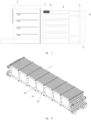
- the present invention provides a coating device for a tube-type PERC solar cell comprising a wafer loading area 1, a furnace body 2, a gas cabinet 3, a vacuum system 4, a heating system 7, a control system 5 and a graphite boat 6, wherein the gas cabinet is provided with a first gas line for feeding silane, a second gas line for feeding ammonia, a third gas line for feeding trimethylaluminum, a fourth gas line for feeding nitrous oxide and a fifth gas line for feeding methane; the first gas line, the second gas line, the third gas line, the fourth gas line and the fifth gas line are disposed inside the gas cabinet 3 and are not illustrated in FIG. 1 .
- the graphite boat 6 is used for loading and unloading a silicon wafer.
- the graphite boat 6 should be pre-processed before use or after several coating, wherein the pre-processing includes two steps: 1. baking the graphite boat; 2. coating the surface of the baked graphite boat with at least one layer of silicon carbide film.
- a preferred implementation of pre-processing includes the following steps.
- an optimal effect of pre-processing the graphite boat may be achieved through the cooperation of the above various parameters with fewer materials, less time and boosted production efficiency.
- a preferred implementation of coating the silicon carbide film contains:
- the graphite boat Before use or after several coating, the graphite boat should be pre-processed, the pre-processing including baking the graphite boat by a heating system and coating the surface of the graphite boat with at least one layer of silicon carbide film by the gas cabinet.
- the pre-processing including baking the graphite boat by a heating system and coating the surface of the graphite boat with at least one layer of silicon carbide film by the gas cabinet.
- the silicon carbide is a semiconductor
- the rear aluminum oxide coating has satisfactory uniformity, which reduces EL defects such as EL black zone and the like.
- the steps of pre-processing the graphite boat are decreased to two steps, i.e., baking and coating of silicon carbide, which saves time and enhances production efficiency.
- the silicon carbide matrix has an extreme small friction coefficient and exhibits a good self-lubricating property.
- the silicon wafer is inserted into the graphite boat, there are fewer scratches on the silicon wafer, which greatly reduces the proportion of the EL scratches and increases the EL yield of the cell.
- the coating device for the tube-type PERC solar cell simplifies the pre-processing steps of the graphite boat, reduces consumption of silicon wafers, avoids scratches on the silicon wafer and boosts the EL yield of the cell.
- the graphite boat 6 is used for loading and unloading silicon wafers.
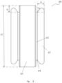
- the graphite boat 6 includes a pin 60 which includes a pin shaft 61, a pin cap 62, and a pin base 63.
- the pin shaft 61 is mounted on the pin base 63.
- the pin cap 62 is connected to the pin shaft 61.
- a pin slot 64 is formed among the pin shaft 61, the pin cap 62, and the pin base 63. The depth of the pin slot 64 is 0.5-1 mm.
- the depth of the pin slot 64, h is preferably 0.6-0.8 mm; the diameter of the pin base 63, D, is preferably 6-15 mm; the angle of inclination of the inclination surface of the pin cap 62, ⁇ , is preferably 35-45 degrees; and the thickness of the pin cap 62, a, is preferably 1-1.3 mm.
- the depth of the pin slot 64 of the graphite boat, h is 0.7-0.8mm; the diameter of the pin base 63, D, is 8-12mm; the angle of inclination of the inclined surface of the pin cap 62, ⁇ , is 37-42 degrees; and the thickness of the pin cap 62, a, is 1.1-1.2mm.
- the depth of the pin slot 64, h is 0.7 mm; the diameter of the pin base 63, D, is 9 mm; the angle of inclination of the inclination surface of the pin cap 62, a, is 40 degrees; and the thickness of the pin cap 62, a, is 1.2 mm.
- the depth h of the pin slot is the depth of the inside of the pin slot, and mainly refers to the depth of the side of the pin shaft 61 that forms an angle with the pin base 63.
- the depth h of the pin slot (the diameter of the pin base - the diameter of the pin shaft) / 2.
- the angle of inclination of the inclination surface of the pin cap 62, ⁇ refers to the angle between the inclination surface of the pin cap and the vertical direction.
- the depth h of the pin slot is 1.75 mm
- the diameter D of the pin base is 9 mm
- the angle of inclination ⁇ of the inclination surface of the pin cap is 30 degrees
- the thickness a of the pin cap is 1 mm.
- the pin slot is deeper, which leads to a too big gap between the silicon wafer and the pin base at the position of the pin; and as a result, a lot of gas reaches and is coated on the rear surface of the silicon wafer, leading to the formation of a large number of boat teeth marks at the front surface edge of the cell.
- the pin cap has a small angle of inclination and a small thickness, leading to small adjustment room for the automatic wafer inserter; and consequentially, it is difficult to effectively lower the occurrence of scratching.
- the silicon wafer can be inserted into the pin slot without contacting the graphite boat wall, during which the silicon wafer is kept at a distance from the graphite boat to avoid friction between the silicon wafer and the graphite boat wall. If the distance between the silicon wafer and the graphite boat plate were too large, scratching would be less likely to take place, but the possibility of the undesirable coating would increase as the silicon wafer would be less easy to be close to the boat wall.
- the silicon wafer may be prevented from being inserted into the pin slot, and the silicon wafer may fall off as a result. If the distance between the silicon wafer and the graphite boat plate were too small, the silicon wafer would be closer to the graphite boat plate. As a result, undesirable coating would be less likely to take place, but the proportion of scratching would increase.
- the position of the boat teeth mark at the edge of the front surface of the cell corresponds to the position of the pin during coating the rear surface by PECVD.
- the mark is formed as a result of gas flowing to the front surface of the cell from the position of the pin. Since the thickness of the pin base is slightly smaller than the thickness of the graphite boat plate, there is a gap between the silicon wafer and the pin base at the position of the pin. When coating the rear surface, the gas enters the gap from two sides below the pin shaft, which causes a film deposited at the front surface edge of the silicon wafer, i.e., forming a semi-circular boat teeth mark.
- the present invention adjusts the diameter D of the pin base and the diameter of the pin shaft to reduce the depth h of the inside of the pin slot.
- the gap between the silicon wafer and the pin base at the position of the pin is reduced; consequentially, the amount of gas reaching and coating the rear surface of the silicon wafer is reduced, and boat teeth marks at the front surface edges are thus much less likely to occur.
- the suction cup releases its vacuum and thus the silicon wafer falls onto the inclined surface ⁇ of the pin cap.
- the silicon wafer slides down the inclined surface until it is close to the graphite boat wall. This type of insertion is contactless and could reduce scratching of the silicon wafer.
- the present invention adequately increases the angle of inclination ⁇ of the inclined surface of the pin cap and the thickness a of the pin cap, and adjusts the automatic wafer inserter, thereby slightly increasing the distance between the silicon wafer and the graphite boat wall on inserting the wafer, reducing scratching.
- Increasing the angle of inclination of the inclined surface of the pin cap reduces the impact force on the silicon wafer from the graphite boat wall when the silicon wafer is sliding down, reducing breakage rate.
- the present invention can avoid undesirable coating during the production process and solve the problem of undesirable coating from its root. No additional process is required, which simplifies the overall process and reduces production cost.
- the invention is of great importance for the solar photovoltaic industry, which is extremely cost-sensitive.
- the present invention also solves the problem of scratching.
- the present invention also discloses a coating method for a tube-type PERC solar cell, comprising:
- the coating method includes:
- the coating method includes:
- undesirable coating mainly occurs during the deposition of silicon nitride. This is because silicon nitride is the outer (top) layer of the rear composite film; and as the deposition time increases, the thickness of the film at the surface of the silicon wafer increases, which causes the silicon wafer to bend. As a result, silane and ammonia are probably coated to the front surface edge of the cell. By shortening the time and temperature of silicon nitride deposition, the bending of the silicon wafer can be reduced, and thus the amount of the undesirable coating can be reduced. Further experiments have shown that the temperature window for silicon nitride deposition is very narrow, between 390-410 degrees; when the temperature is further lowered, the amount of the undesirable coating increases, however.
- the plasma power is set to 2000-5000w; when depositing the silicon oxynitride film, the plasma power is set to 4000-6000w; when depositing the silicon nitride film, the plasma power is set to 10000-13000w; and when depositing the silicon dioxide film, the plasma power is set to 2000-5000w. This ensures that different layers have good deposition rates and improves deposition uniformity.
- the coating method for the tube-type PERC solar cell can simplify the pre-processing steps of the graphite boat, reduce consumption of silicon wafers, avoid scratches on the silicon wafer, reduce EL defects such as EL black zone and the like and enhance the EL yield of the cell.
- the present invention adjusts the diameters of the pin shaft and the pin base to reduce the depth of the inside of the pin slot. As a result, the gap between the silicon wafer and the pin base at the position of the pin is reduced. Further, the amount of gas reaching and coating the rear surface of the silicon wafer is reduced, and boat teeth marks at the front surface edges of the cell thus are much less likely to occur.
- the present invention adequately increases the angle of inclination of the inclined surface of the pin cap and the thickness of the pin cap, and adjusts the automatic wafer inserter, thereby slightly increasing the distance between the silicon wafer and the graphite boat wall on inserting the wafer, and reducing scratching. Meanwhile, it is possible to reduce the impact force on the silicon wafer from the graphite boat wall when the silicon wafer is sliding down, reducing breakage rate.
- the present invention provides a coating method for a tube-type PERC solar cell.
- a coating method for a tube-type PERC solar cell Prior to the coating of the rear composite film, it is only required to pre-process the graphite boat with two steps (baking + coating of silicon carbide), without coating the boat with a wafer inserted like the prior art. This greatly reduces the consumption of silicon wafers, prevents the silicon wafer from bending a lot due to a thick coating on its surface, saves production time and enhances production efficiency.
- the silicon carbide matrix has an extreme small friction coefficient and exhibits a good self-lubricating property. On this account, when the silicon wafer is inserted into the graphite boat, there are fewer scratches on the silicon wafer, which greatly reduces the proportion of the EL scratches and increases the EL yield of the cell.
- the deposition temperature for silicon nitride is set to 390-410°C, and the deposition time is set within 100-400s, according to the present invention.
- the bending of the silicon wafer can be reduced, and thus the amount of the undesirable coating can be reduced.
- the temperature window for silicon nitride deposition is very narrow, between 390-410 °C, which may allow the maximum reduction of the undesirable coating.
- the deposition temperature is below 390°C, the amount of the undesirable coating increases, however.
Landscapes
- Chemical & Material Sciences (AREA)
- Engineering & Computer Science (AREA)
- General Chemical & Material Sciences (AREA)
- Chemical Kinetics & Catalysis (AREA)
- Materials Engineering (AREA)
- Mechanical Engineering (AREA)
- Metallurgy (AREA)
- Organic Chemistry (AREA)
- Inorganic Chemistry (AREA)
- Physics & Mathematics (AREA)
- Plasma & Fusion (AREA)
- Chemical Vapour Deposition (AREA)
- Life Sciences & Earth Sciences (AREA)
- Sustainable Development (AREA)
- Sustainable Energy (AREA)
- Formation Of Insulating Films (AREA)
Claims (6)
- Beschichtungsverfahren für eine röhrenförmige PERC-Solarzelle, dadurch gekennzeichnet, dass es umfasst:(1) Einsetzen eines Graphitschiffchens (6) in eine röhrenförmige PECVD-Beschichtungsvorrichtung zum Backen des Graphitschiffchens bei einer Temperatur von 300-480°C für 10-60 Minuten;(2) erneutes Einsetzen des gebackenen und entnommenen Graphitschiffchens in die röhrenförmige PECVD-Beschichtungsvorrichtung, um eine Oberfläche des Graphitschiffchens mit mindestens einer Schicht aus Siliciumcarbid zu beschichten; und(3) Platzieren eines bearbeiteten Siliziumwafers auf dem Graphitschiffchen und Einführen des bearbeiteten Siliziumwafers über das Graphitschiffchen in die röhrenförmige PECVD-Beschichtungsvorrichtung, um einen rückwärtigen Verbundfilm auf einer Oberfläche des Siliziumwafers zu bilden, wobei der rückwärtige Verbundfilm einen Aluminiumoxidfilm, einen Siliziumdioxidfilm, einen Siliziumoxynitridfilm und einen Siliziumnitridfilm umfasst.
- Beschichtungsverfahren nach Anspruch 1 für eine rohrförmigen PERC-Solarzelle, gekennzeichnet durch:(1) Einsetzen des Graphitschiffchens in die röhrenförmige PECVD-Beschichtungsvorrichtung zum Backen des Graphitschiffchens bei einer Temperatur von 300-480°C für 10-60 Minuten;(2) erneutes Einsetzen des gebackenen und entnommenen Graphitschiffchens in die röhrenförmige PECVD-Beschichtungsvorrichtung, um die Oberfläche des Graphitschiffchens mit der mindestens einen Schicht aus Siliciumcarbidfilm zu beschichten, wobei ein Verfahren zum Beschichten des Siliciumcarbidfilms umfasst:Erhöhen der Temperatur auf 380-480°C und Zuführen von Ammoniak mit einer Durchflussrate von 1-8 slm für 2-10 min bei einer Plasmaleistung von 2000-5000 W;Zuführen von Methan mit einer Durchflussrate von 2-8 slm und Silan mit einer Durchflussrate von 200-800 sccm für 5-30 s;Zuführen von Methan mit einer Durchflussrate von 2-8 slm und Silan mit einer Durchflussrate von 200-800 sccm für 1-4 Stunden bei einer Plasmaleistung von 3000-10000 W; undAbsenken der Temperatur auf 350-400°C und Entnehmen des Graphitschiffchens; und(3) Platzieren des bearbeiteten Siliziumwafers auf dem Graphitschiffchen und Einführen des bearbeiteten Siliziumwafers über das Graphitschiffchen in die röhrenförmige PECVD-Beschichtungsvorrichtung, um den hinteren Verbundfilm zu bilden, wobei ein Verfahren zum Beschichten des hinteren Verbundfilms umfasst:Abscheiden des Aluminiumoxidfilms unter Verwendung von TMA und N2O, wobei die Gasflussrate von TMA 250-500 sccm, das Verhältnis von TMA zu N2O 1 zu 15-25 und die Plasmaleistung 2000-5000 W beträgt;Abscheiden des Siliziumoxynitridfilms unter Verwendung von Silan, Ammoniak und Distickstoffoxid, wobei die Gasdurchflussrate von Silan 50-200 sccm, das Verhältnis von Silan zu Distickstoffoxid 1 zu 10-80, die Durchflussrate von Ammoniak 0,1-5 slm und die Plasmaleistung 4000-6000 W beträgt;Abscheiden des Siliziumnitridfilms unter Verwendung von Silan und Ammoniak, wobei die Gasflussrate von Silan 500-1000 sccm beträgt, ein Verhältnis von Silan zu Ammoniak 1 zu 6-15 ist, eine Abscheidungstemperatur von Siliziumnitrid 390-410 °C ist, eine Abscheidungszeit 100-400 s ist und die Plasmaleistung 10000-13000 W ist; undAbscheiden des Siliziumdioxidfilms unter Verwendung von Distickstoffoxid, wobei die Durchflussrate des Distickstoffoxids 0,1-5 slm und die Plasmaleistung 2000-5000 W beträgt.
- Beschichtungsverfahren nach Anspruch 2 für eine röhrenförmige PERC-Solarzelle, gekennzeichnet durch:(1) Einsetzen des Graphitschiffchens in die röhrenförmige PECVD-Beschichtungsvorrichtung zum Backen des Graphitschiffchens bei einer Temperatur von 320-420°C für 20-40 Minuten;(2) erneutes Einsetzen des gebackenen und entnommenen Graphitschiffchens in die röhrenförmige PECVD-Beschichtungsvorrichtung, um die Oberfläche des Graphitschiffchens mit der mindestens einen Schicht aus Siliciumcarbidfilm zu beschichten, wobei ein Verfahren zum Beschichten des Siliciumcarbidfilms umfasst:Erhöhen der Temperatur auf 400-460°C und Zuführen von Ammoniak mit einer Durchflussrate von 2-6 slm für 3-8 min bei einer Plasmaleistung von 3000-4000 W;Zuführen von Methan mit einer Durchflussrate von 3-6 slm und Silan mit einer Durchflussrate von 300-600 sccm für 10-20 s;Zuführen von Methan mit einer Durchflussrate von 3-6 slm und Silan mit einer Durchflussrate von 300-600 sccm für 2-3 Stunden bei einer Plasmaleistung von 5000-8000 W; undAbsenkeng der Temperatur auf 370-390°C und Entnehmen des Graphitschiffchens; und(3) Platzieren eines bearbeiteten Siliziumwafers auf dem Graphitschiffchen und Senden des bearbeiteten Siliziumwafers über das Graphitschiffchen in die röhrenförmige PECVD-Beschichtungsvorrichtung, um den hinteren Verbundfilm zu bilden, wobei ein Verfahren zum Beschichten des hinteren Verbundfilms umfasst:Abscheiden des Aluminiumoxidfilms unter Verwendung von TMA und N2O, wobei die Gasflussrate von TMA 250-500 sccm beträgt, das Verhältnis von TMA zu N2O 1 bis 15-25 beträgt, die Abscheidungstemperatur des Aluminiumoxidfilms 250-300 °C beträgt, die Abscheidungszeit 50-300 s beträgt und die Plasmaleistung 2000-5000 W beträgt;Abscheiden des Siliciumoxynitridfilms unter Verwendung von Silan, Ammoniak und Distickstoffoxid, wobei die Gasdurchflussrate von Silan 50-200 sccm, das Verhältnis von Silan zu Distickstoffoxid 1 zu 10-80, die Durchflussrate von Ammoniak 0,1-5 slm, die Abscheidungstemperatur des Siliciumoxynitridfilms 350-410 °C, die Abscheidungszeit 50-200 s und die Plasmaleistung 4000-6000 W beträgt;Abscheiden des Siliciumnitridfilms unter Verwendung von Silan und Ammoniak, wobei eine Gasflussrate von Silan 500-1000 sccm beträgt, ein Verhältnis von Silan zu Ammoniak 1 zu 6-15 beträgt, eine Abscheidungstemperatur des Siliciumnitridfilms 390-410 °C beträgt, eine Abscheidungszeit 100-400 s beträgt und die Plasmaleistung 10000-13000 W beträgt; undAbscheiden des Siliziumdioxidfilms unter Verwendung von Distickstoffoxid, wobei die Durchflussrate des Distickstoffoxids 0,1-5 slm und die Plasmaleistung 2000-5000 W beträgt.
- Beschichtungsverfahren nach Anspruch 1 für eine röhrenförmige PERC-Solarzelle, wobei das Graphitschiffchen einen Stift enthält, der einen Stiftschaft, eine Stiftkappe und eine Stiftbasis aufweist; der Stiftschaft auf der Stiftbasis montiert ist; die Stiftkappe mit dem Stiftschaft verbunden ist; ein Stiftschlitz zwischen dem Stiftschaft, der Stiftkappe und der Stiftbasis ausgebildet ist; und eine Tiefe des Stiftschlitzes 0,5-1 mm beträgt.
- Beschichtungsverfahren nach Anspruch 4 für eine röhrenförmige PERC-Solarzelle, wobei der Stiftschlitz des Graphitschiffchens eine Tiefe von 0,6-0,8 mm hat, ein Durchmesser der Stiftbasis 6-15 mm beträgt, ein Neigungswinkel einer geneigten Oberfläche der Stiftkappe 35-45 Grad beträgt und eine Dicke der Stiftkappe 1-1,3 mm beträgt.
- Beschichtungsverfahren nach Anspruch 5 für eine röhrenförmige PERC-Solarzelle, wobei der Stiftschlitz des Graphitschiffchens eine Tiefe von 0,7-0,8 mm hat, der Durchmesser der Stiftbasis 8-12 mm beträgt, der Neigungswinkel der geneigten Oberfläche der Stiftkappe 37-42 Grad beträgt und die Dicke der Stiftkappe 1,1-1,2 mm beträgt.
Applications Claiming Priority (1)
| Application Number | Priority Date | Filing Date | Title |
|---|---|---|---|
| PCT/CN2017/087443 WO2018223314A1 (zh) | 2017-06-07 | 2017-06-07 | 管式perc太阳能电池的镀膜设备及镀膜方法 |
Publications (3)
| Publication Number | Publication Date |
|---|---|
| EP3636799A1 EP3636799A1 (de) | 2020-04-15 |
| EP3636799A4 EP3636799A4 (de) | 2021-01-27 |
| EP3636799B1 true EP3636799B1 (de) | 2023-08-02 |
Family
ID=64565683
Family Applications (1)
| Application Number | Title | Priority Date | Filing Date |
|---|---|---|---|
| EP17912428.4A Active EP3636799B1 (de) | 2017-06-07 | 2017-06-07 | Beschichtungsverfahren für rohrartige perc-solarzellen |
Country Status (5)
| Country | Link |
|---|---|
| US (1) | US20200199746A1 (de) |
| EP (1) | EP3636799B1 (de) |
| JP (1) | JP6951476B2 (de) |
| KR (1) | KR102299855B1 (de) |
| WO (1) | WO2018223314A1 (de) |
Families Citing this family (7)
| Publication number | Priority date | Publication date | Assignee | Title |
|---|---|---|---|---|
| CN111081618A (zh) * | 2019-12-20 | 2020-04-28 | 晋能光伏技术有限责任公司 | 一种pecvd石墨舟的电池片插片方法和pecvd石墨舟 |
| CN113481487A (zh) * | 2021-07-06 | 2021-10-08 | 横店集团东磁股份有限公司 | 一种太阳能电池片及其背面pecvd法和应用 |
| CN113584462A (zh) * | 2021-07-15 | 2021-11-02 | 大连连城数控机器股份有限公司 | 一种可镀多种膜的管式pecvd石墨舟镀膜工艺 |
| CN113430503B (zh) * | 2021-07-15 | 2024-10-11 | 连科半导体有限公司 | 一种可镀多种膜的管式pecvd石墨舟结构 |
| CN114059015A (zh) * | 2021-11-01 | 2022-02-18 | 浙江爱旭太阳能科技有限公司 | 一种载板的烘烤系统和烘烤方法 |
| CN115652291A (zh) * | 2022-09-29 | 2023-01-31 | 浙江求是半导体设备有限公司 | 硅片的沉积控制方法、装置、沉积设备及计算机设备 |
| CN116623154B (zh) * | 2023-05-23 | 2024-01-02 | 东莞嘉拓日晟智能科技有限公司 | 一种管式pecvd设备及其镀膜工艺 |
Family Cites Families (14)
| Publication number | Priority date | Publication date | Assignee | Title |
|---|---|---|---|---|
| JPH03228896A (ja) * | 1989-09-26 | 1991-10-09 | Tokuzo Sukegawa | 結晶成長用無機物品 |
| JPH05121339A (ja) * | 1992-03-26 | 1993-05-18 | Semiconductor Energy Lab Co Ltd | 被膜作製装置 |
| JPH10106959A (ja) * | 1996-09-26 | 1998-04-24 | Nippon Carbon Co Ltd | プラズマcvd装置用円板状黒鉛集成体 |
| US9040170B2 (en) * | 2004-09-20 | 2015-05-26 | Global Oled Technology Llc | Electroluminescent device with quinazoline complex emitter |
| CN101024213A (zh) * | 2006-02-21 | 2007-08-29 | 陈国栋 | 晶片承载盘保护层的制造方法 |
| KR20140117420A (ko) * | 2012-01-03 | 2014-10-07 | 어플라이드 머티어리얼스, 인코포레이티드 | Si 태양 전지들의 표면 부동태화의 성능 및 안정성을 개선하기 위한 버퍼 층 |
| KR20140116120A (ko) * | 2012-01-03 | 2014-10-01 | 어플라이드 머티어리얼스, 인코포레이티드 | 결정질 실리콘 태양 전지들을 패시베이팅하기 위한 진보된 플랫폼 |
| CN104419909B (zh) * | 2013-08-27 | 2016-12-28 | 茂迪(苏州)新能源有限公司 | 一种镀膜炉管 |
| CN103628042B (zh) * | 2013-12-10 | 2016-04-27 | 浙江正泰太阳能科技有限公司 | 一种改善晶硅电池镀膜质量的方法 |
| CN103996741B (zh) * | 2014-05-20 | 2016-04-06 | 奥特斯维能源(太仓)有限公司 | 一种太阳能电池石墨舟及其镀膜方法 |
| JP6176811B2 (ja) * | 2014-06-25 | 2017-08-09 | 株式会社日立国際電気 | 半導体装置の製造方法、基板処理装置およびプログラム |
| JP6368282B2 (ja) * | 2015-06-29 | 2018-08-01 | クアーズテック株式会社 | ウエハボート及びその製造方法 |
| CN106531839A (zh) * | 2015-09-11 | 2017-03-22 | 镇江鹏飞光伏技术有限公司 | 石墨舟直型槽工艺点及其生产工艺 |
| CN205170969U (zh) * | 2015-10-20 | 2016-04-20 | 浙江晶科能源有限公司 | Pecvd用石墨舟卡点 |
-
2017
- 2017-06-07 EP EP17912428.4A patent/EP3636799B1/de active Active
- 2017-06-07 JP JP2019567618A patent/JP6951476B2/ja not_active Expired - Fee Related
- 2017-06-07 KR KR1020197033717A patent/KR102299855B1/ko not_active Expired - Fee Related
- 2017-06-07 WO PCT/CN2017/087443 patent/WO2018223314A1/zh not_active Ceased
- 2017-06-07 US US16/620,339 patent/US20200199746A1/en not_active Abandoned
Non-Patent Citations (1)
| Title |
|---|
| 32TH EUROPEAN PHOTOVOLTAIC SOLAR ENERGY CONFERENCE, PROCEEDINGS OF THE 32TH INTERNATIONAL CONFERENCE, WIP-RENEWABLE ENERGIES, SYLVENSTEINSTR. 2 81369 MUNICH, GERMANY, 22 July 2016 (2016-07-22), XP040679714, ISBN: 978-3-936338-41-6 * |
Also Published As
| Publication number | Publication date |
|---|---|
| JP6951476B2 (ja) | 2021-10-20 |
| US20200199746A1 (en) | 2020-06-25 |
| KR20200006062A (ko) | 2020-01-17 |
| WO2018223314A1 (zh) | 2018-12-13 |
| EP3636799A1 (de) | 2020-04-15 |
| EP3636799A4 (de) | 2021-01-27 |
| KR102299855B1 (ko) | 2021-09-08 |
| JP2020522896A (ja) | 2020-07-30 |
Similar Documents
| Publication | Publication Date | Title |
|---|---|---|
| EP3636799B1 (de) | Beschichtungsverfahren für rohrartige perc-solarzellen | |
| CN107287579B (zh) | 管式perc太阳能电池的镀膜设备及镀膜方法 | |
| US11848395B2 (en) | Preparation method for bifacial perc solar cell | |
| US20200212242A1 (en) | Monofacial tube-type perc solar cell, preparation method thereof, and production device therefor | |
| US8247022B2 (en) | Silicon nitride passivation for a solar cell | |
| US20110272024A1 (en) | MULTI-LAYER SiN FOR FUNCTIONAL AND OPTICAL GRADED ARC LAYERS ON CRYSTALLINE SOLAR CELLS | |
| CN108695408B (zh) | 一种管式pecvd沉积氮化硅叠层减反射膜工艺 | |
| CN104094418A (zh) | 硅基太阳能电池的钝化薄膜堆叠 | |
| TW201427036A (zh) | 用於結晶矽太陽能電池之最佳化的抗反射塗層 | |
| WO2023092977A1 (zh) | 制备隧穿氧化层和非晶硅薄膜的方法及TOPCon电池 | |
| CN112510100A (zh) | 一种perc电池的背面钝化膜结构及其制备方法和用途 | |
| CN112838143A (zh) | 一种perc电池中氧化铝膜的沉积方法 | |
| US20040235286A1 (en) | Method of depositing an oxide layer on a substrate and a photovoltaic cell using said substrate | |
| CN102386277B (zh) | 多层镀膜工艺 | |
| CN108470800A (zh) | 一种降低pecvd机台tma耗量的方法 | |
| CN206893626U (zh) | 管式perc单面太阳能电池 | |
| Chae et al. | Ultrafast deposition of microcrystalline Si by thermal plasma chemical vapor deposition | |
| CN106935682A (zh) | 一种清除单晶硅电池片烧结后脏片的工艺 | |
| CN117431526A (zh) | 一种N型TOPCon电池镀膜工艺 | |
| CN206902232U (zh) | 管式pecvd设备 | |
| CN104952978A (zh) | 一种太阳能电池镀膜工艺 | |
| CN113930748B (zh) | 太阳能电池的制备方法、太阳能电池与光伏组件 | |
| CN120475806B (zh) | N型太阳能电池及其制备方法 | |
| CN120111987B (zh) | 一种制备掺氧微晶硅薄膜的方法及设备 | |
| CN120076448A (zh) | 太阳能电池背钝化膜及其制备方法、太阳能电池及其制备方法 |
Legal Events
| Date | Code | Title | Description |
|---|---|---|---|
| STAA | Information on the status of an ep patent application or granted ep patent |
Free format text: STATUS: THE INTERNATIONAL PUBLICATION HAS BEEN MADE |
|
| PUAI | Public reference made under article 153(3) epc to a published international application that has entered the european phase |
Free format text: ORIGINAL CODE: 0009012 |
|
| STAA | Information on the status of an ep patent application or granted ep patent |
Free format text: STATUS: REQUEST FOR EXAMINATION WAS MADE |
|
| 17P | Request for examination filed |
Effective date: 20200107 |
|
| AK | Designated contracting states |
Kind code of ref document: A1 Designated state(s): AL AT BE BG CH CY CZ DE DK EE ES FI FR GB GR HR HU IE IS IT LI LT LU LV MC MK MT NL NO PL PT RO RS SE SI SK SM TR |
|
| AX | Request for extension of the european patent |
Extension state: BA ME |
|
| DAV | Request for validation of the european patent (deleted) | ||
| DAX | Request for extension of the european patent (deleted) | ||
| A4 | Supplementary search report drawn up and despatched |
Effective date: 20210114 |
|
| RIC1 | Information provided on ipc code assigned before grant |
Ipc: C23C 16/34 20060101ALI20201223BHEP Ipc: C23C 16/458 20060101ALI20201223BHEP Ipc: C23C 16/30 20060101ALI20201223BHEP Ipc: C23C 16/32 20060101ALI20201223BHEP Ipc: C23C 16/50 20060101ALI20201223BHEP Ipc: C23C 16/40 20060101ALI20201223BHEP Ipc: C23C 16/455 20060101AFI20201223BHEP Ipc: C23C 16/44 20060101ALI20201223BHEP Ipc: H01L 31/18 20060101ALI20201223BHEP |
|
| GRAP | Despatch of communication of intention to grant a patent |
Free format text: ORIGINAL CODE: EPIDOSNIGR1 |
|
| STAA | Information on the status of an ep patent application or granted ep patent |
Free format text: STATUS: GRANT OF PATENT IS INTENDED |
|
| INTG | Intention to grant announced |
Effective date: 20230413 |
|
| GRAS | Grant fee paid |
Free format text: ORIGINAL CODE: EPIDOSNIGR3 |
|
| GRAA | (expected) grant |
Free format text: ORIGINAL CODE: 0009210 |
|
| STAA | Information on the status of an ep patent application or granted ep patent |
Free format text: STATUS: THE PATENT HAS BEEN GRANTED |
|
| AK | Designated contracting states |
Kind code of ref document: B1 Designated state(s): AL AT BE BG CH CY CZ DE DK EE ES FI FR GB GR HR HU IE IS IT LI LT LU LV MC MK MT NL NO PL PT RO RS SE SI SK SM TR |
|
| REG | Reference to a national code |
Ref country code: GB Ref legal event code: FG4D |
|
| REG | Reference to a national code |
Ref country code: CH Ref legal event code: EP |
|
| REG | Reference to a national code |
Ref country code: DE Ref legal event code: R096 Ref document number: 602017072333 Country of ref document: DE |
|
| REG | Reference to a national code |
Ref country code: IE Ref legal event code: FG4D |
|
| REG | Reference to a national code |
Ref country code: LT Ref legal event code: MG9D |
|
| REG | Reference to a national code |
Ref country code: NL Ref legal event code: MP Effective date: 20230802 |
|
| REG | Reference to a national code |
Ref country code: AT Ref legal event code: MK05 Ref document number: 1594828 Country of ref document: AT Kind code of ref document: T Effective date: 20230802 |
|
| PG25 | Lapsed in a contracting state [announced via postgrant information from national office to epo] |
Ref country code: GR Free format text: LAPSE BECAUSE OF FAILURE TO SUBMIT A TRANSLATION OF THE DESCRIPTION OR TO PAY THE FEE WITHIN THE PRESCRIBED TIME-LIMIT Effective date: 20231103 |
|
| PG25 | Lapsed in a contracting state [announced via postgrant information from national office to epo] |
Ref country code: IS Free format text: LAPSE BECAUSE OF FAILURE TO SUBMIT A TRANSLATION OF THE DESCRIPTION OR TO PAY THE FEE WITHIN THE PRESCRIBED TIME-LIMIT Effective date: 20231202 |
|
| PG25 | Lapsed in a contracting state [announced via postgrant information from national office to epo] |
Ref country code: SE Free format text: LAPSE BECAUSE OF FAILURE TO SUBMIT A TRANSLATION OF THE DESCRIPTION OR TO PAY THE FEE WITHIN THE PRESCRIBED TIME-LIMIT Effective date: 20230802 Ref country code: RS Free format text: LAPSE BECAUSE OF FAILURE TO SUBMIT A TRANSLATION OF THE DESCRIPTION OR TO PAY THE FEE WITHIN THE PRESCRIBED TIME-LIMIT Effective date: 20230802 Ref country code: PT Free format text: LAPSE BECAUSE OF FAILURE TO SUBMIT A TRANSLATION OF THE DESCRIPTION OR TO PAY THE FEE WITHIN THE PRESCRIBED TIME-LIMIT Effective date: 20231204 Ref country code: NO Free format text: LAPSE BECAUSE OF FAILURE TO SUBMIT A TRANSLATION OF THE DESCRIPTION OR TO PAY THE FEE WITHIN THE PRESCRIBED TIME-LIMIT Effective date: 20231102 Ref country code: NL Free format text: LAPSE BECAUSE OF FAILURE TO SUBMIT A TRANSLATION OF THE DESCRIPTION OR TO PAY THE FEE WITHIN THE PRESCRIBED TIME-LIMIT Effective date: 20230802 Ref country code: LV Free format text: LAPSE BECAUSE OF FAILURE TO SUBMIT A TRANSLATION OF THE DESCRIPTION OR TO PAY THE FEE WITHIN THE PRESCRIBED TIME-LIMIT Effective date: 20230802 Ref country code: LT Free format text: LAPSE BECAUSE OF FAILURE TO SUBMIT A TRANSLATION OF THE DESCRIPTION OR TO PAY THE FEE WITHIN THE PRESCRIBED TIME-LIMIT Effective date: 20230802 Ref country code: IS Free format text: LAPSE BECAUSE OF FAILURE TO SUBMIT A TRANSLATION OF THE DESCRIPTION OR TO PAY THE FEE WITHIN THE PRESCRIBED TIME-LIMIT Effective date: 20231202 Ref country code: HR Free format text: LAPSE BECAUSE OF FAILURE TO SUBMIT A TRANSLATION OF THE DESCRIPTION OR TO PAY THE FEE WITHIN THE PRESCRIBED TIME-LIMIT Effective date: 20230802 Ref country code: GR Free format text: LAPSE BECAUSE OF FAILURE TO SUBMIT A TRANSLATION OF THE DESCRIPTION OR TO PAY THE FEE WITHIN THE PRESCRIBED TIME-LIMIT Effective date: 20231103 Ref country code: FI Free format text: LAPSE BECAUSE OF FAILURE TO SUBMIT A TRANSLATION OF THE DESCRIPTION OR TO PAY THE FEE WITHIN THE PRESCRIBED TIME-LIMIT Effective date: 20230802 Ref country code: AT Free format text: LAPSE BECAUSE OF FAILURE TO SUBMIT A TRANSLATION OF THE DESCRIPTION OR TO PAY THE FEE WITHIN THE PRESCRIBED TIME-LIMIT Effective date: 20230802 |
|
| PG25 | Lapsed in a contracting state [announced via postgrant information from national office to epo] |
Ref country code: PL Free format text: LAPSE BECAUSE OF FAILURE TO SUBMIT A TRANSLATION OF THE DESCRIPTION OR TO PAY THE FEE WITHIN THE PRESCRIBED TIME-LIMIT Effective date: 20230802 |
|
| PG25 | Lapsed in a contracting state [announced via postgrant information from national office to epo] |
Ref country code: ES Free format text: LAPSE BECAUSE OF FAILURE TO SUBMIT A TRANSLATION OF THE DESCRIPTION OR TO PAY THE FEE WITHIN THE PRESCRIBED TIME-LIMIT Effective date: 20230802 |
|
| PG25 | Lapsed in a contracting state [announced via postgrant information from national office to epo] |
Ref country code: SM Free format text: LAPSE BECAUSE OF FAILURE TO SUBMIT A TRANSLATION OF THE DESCRIPTION OR TO PAY THE FEE WITHIN THE PRESCRIBED TIME-LIMIT Effective date: 20230802 Ref country code: RO Free format text: LAPSE BECAUSE OF FAILURE TO SUBMIT A TRANSLATION OF THE DESCRIPTION OR TO PAY THE FEE WITHIN THE PRESCRIBED TIME-LIMIT Effective date: 20230802 Ref country code: ES Free format text: LAPSE BECAUSE OF FAILURE TO SUBMIT A TRANSLATION OF THE DESCRIPTION OR TO PAY THE FEE WITHIN THE PRESCRIBED TIME-LIMIT Effective date: 20230802 Ref country code: EE Free format text: LAPSE BECAUSE OF FAILURE TO SUBMIT A TRANSLATION OF THE DESCRIPTION OR TO PAY THE FEE WITHIN THE PRESCRIBED TIME-LIMIT Effective date: 20230802 Ref country code: DK Free format text: LAPSE BECAUSE OF FAILURE TO SUBMIT A TRANSLATION OF THE DESCRIPTION OR TO PAY THE FEE WITHIN THE PRESCRIBED TIME-LIMIT Effective date: 20230802 Ref country code: CZ Free format text: LAPSE BECAUSE OF FAILURE TO SUBMIT A TRANSLATION OF THE DESCRIPTION OR TO PAY THE FEE WITHIN THE PRESCRIBED TIME-LIMIT Effective date: 20230802 Ref country code: SK Free format text: LAPSE BECAUSE OF FAILURE TO SUBMIT A TRANSLATION OF THE DESCRIPTION OR TO PAY THE FEE WITHIN THE PRESCRIBED TIME-LIMIT Effective date: 20230802 |
|
| REG | Reference to a national code |
Ref country code: DE Ref legal event code: R097 Ref document number: 602017072333 Country of ref document: DE |
|
| PG25 | Lapsed in a contracting state [announced via postgrant information from national office to epo] |
Ref country code: IT Free format text: LAPSE BECAUSE OF FAILURE TO SUBMIT A TRANSLATION OF THE DESCRIPTION OR TO PAY THE FEE WITHIN THE PRESCRIBED TIME-LIMIT Effective date: 20230802 |
|
| PLBE | No opposition filed within time limit |
Free format text: ORIGINAL CODE: 0009261 |
|
| STAA | Information on the status of an ep patent application or granted ep patent |
Free format text: STATUS: NO OPPOSITION FILED WITHIN TIME LIMIT |
|
| 26N | No opposition filed |
Effective date: 20240503 |
|
| PG25 | Lapsed in a contracting state [announced via postgrant information from national office to epo] |
Ref country code: SI Free format text: LAPSE BECAUSE OF FAILURE TO SUBMIT A TRANSLATION OF THE DESCRIPTION OR TO PAY THE FEE WITHIN THE PRESCRIBED TIME-LIMIT Effective date: 20230802 |
|
| PG25 | Lapsed in a contracting state [announced via postgrant information from national office to epo] |
Ref country code: BG Free format text: LAPSE BECAUSE OF FAILURE TO SUBMIT A TRANSLATION OF THE DESCRIPTION OR TO PAY THE FEE WITHIN THE PRESCRIBED TIME-LIMIT Effective date: 20230802 |
|
| PG25 | Lapsed in a contracting state [announced via postgrant information from national office to epo] |
Ref country code: BG Free format text: LAPSE BECAUSE OF FAILURE TO SUBMIT A TRANSLATION OF THE DESCRIPTION OR TO PAY THE FEE WITHIN THE PRESCRIBED TIME-LIMIT Effective date: 20230802 |
|
| REG | Reference to a national code |
Ref country code: DE Ref legal event code: R119 Ref document number: 602017072333 Country of ref document: DE |
|
| PG25 | Lapsed in a contracting state [announced via postgrant information from national office to epo] |
Ref country code: MC Free format text: LAPSE BECAUSE OF FAILURE TO SUBMIT A TRANSLATION OF THE DESCRIPTION OR TO PAY THE FEE WITHIN THE PRESCRIBED TIME-LIMIT Effective date: 20230802 |
|
| REG | Reference to a national code |
Ref country code: CH Ref legal event code: PL |
|
| PG25 | Lapsed in a contracting state [announced via postgrant information from national office to epo] |
Ref country code: LU Free format text: LAPSE BECAUSE OF NON-PAYMENT OF DUE FEES Effective date: 20240607 |
|
| GBPC | Gb: european patent ceased through non-payment of renewal fee |
Effective date: 20240607 |
|
| PG25 | Lapsed in a contracting state [announced via postgrant information from national office to epo] |
Ref country code: DE Free format text: LAPSE BECAUSE OF NON-PAYMENT OF DUE FEES Effective date: 20250101 |
|
| PG25 | Lapsed in a contracting state [announced via postgrant information from national office to epo] |
Ref country code: IE Free format text: LAPSE BECAUSE OF NON-PAYMENT OF DUE FEES Effective date: 20240607 |
|
| PG25 | Lapsed in a contracting state [announced via postgrant information from national office to epo] |
Ref country code: BE Free format text: LAPSE BECAUSE OF NON-PAYMENT OF DUE FEES Effective date: 20240630 Ref country code: CH Free format text: LAPSE BECAUSE OF NON-PAYMENT OF DUE FEES Effective date: 20240630 |
|
| PG25 | Lapsed in a contracting state [announced via postgrant information from national office to epo] |
Ref country code: FR Free format text: LAPSE BECAUSE OF NON-PAYMENT OF DUE FEES Effective date: 20240630 |
|
| PG25 | Lapsed in a contracting state [announced via postgrant information from national office to epo] |
Ref country code: GB Free format text: LAPSE BECAUSE OF NON-PAYMENT OF DUE FEES Effective date: 20240607 |
|
| REG | Reference to a national code |
Ref country code: BE Ref legal event code: MM Effective date: 20240630 |
|
| PG25 | Lapsed in a contracting state [announced via postgrant information from national office to epo] |
Ref country code: CY Free format text: LAPSE BECAUSE OF FAILURE TO SUBMIT A TRANSLATION OF THE DESCRIPTION OR TO PAY THE FEE WITHIN THE PRESCRIBED TIME-LIMIT; INVALID AB INITIO Effective date: 20170607 |
|
| PG25 | Lapsed in a contracting state [announced via postgrant information from national office to epo] |
Ref country code: HU Free format text: LAPSE BECAUSE OF FAILURE TO SUBMIT A TRANSLATION OF THE DESCRIPTION OR TO PAY THE FEE WITHIN THE PRESCRIBED TIME-LIMIT; INVALID AB INITIO Effective date: 20170607 |