EP3637148B1 - Détecteur de noyau - Google Patents
Détecteur de noyau Download PDFInfo
- Publication number
- EP3637148B1 EP3637148B1 EP17919078.0A EP17919078A EP3637148B1 EP 3637148 B1 EP3637148 B1 EP 3637148B1 EP 17919078 A EP17919078 A EP 17919078A EP 3637148 B1 EP3637148 B1 EP 3637148B1
- Authority
- EP
- European Patent Office
- Prior art keywords
- light guide
- scintillation crystal
- slit
- nuclear detector
- array
- Prior art date
- Legal status (The legal status is an assumption and is not a legal conclusion. Google has not performed a legal analysis and makes no representation as to the accuracy of the status listed.)
- Active
Links
Images


Classifications
-
- G—PHYSICS
- G01—MEASURING; TESTING
- G01T—MEASUREMENT OF NUCLEAR OR X-RADIATION
- G01T1/00—Measuring X-radiation, gamma radiation, corpuscular radiation, or cosmic radiation
- G01T1/16—Measuring radiation intensity
- G01T1/161—Applications in the field of nuclear medicine, e.g. in vivo counting
- G01T1/164—Scintigraphy
- G01T1/1641—Static instruments for imaging the distribution of radioactivity in one or two dimensions using one or several scintillating elements; Radio-isotope cameras
- G01T1/1642—Static instruments for imaging the distribution of radioactivity in one or two dimensions using one or several scintillating elements; Radio-isotope cameras using a scintillation crystal and position sensing photodetector arrays, e.g. ANGER cameras
-
- G—PHYSICS
- G01—MEASURING; TESTING
- G01T—MEASUREMENT OF NUCLEAR OR X-RADIATION
- G01T1/00—Measuring X-radiation, gamma radiation, corpuscular radiation, or cosmic radiation
- G01T1/16—Measuring radiation intensity
- G01T1/20—Measuring radiation intensity with scintillation detectors
- G01T1/2018—Scintillation-photodiode combinations
- G01T1/20185—Coupling means between the photodiode and the scintillator, e.g. optical couplings using adhesives with wavelength-shifting fibres
-
- G—PHYSICS
- G01—MEASURING; TESTING
- G01T—MEASUREMENT OF NUCLEAR OR X-RADIATION
- G01T1/00—Measuring X-radiation, gamma radiation, corpuscular radiation, or cosmic radiation
- G01T1/16—Measuring radiation intensity
- G01T1/20—Measuring radiation intensity with scintillation detectors
- G01T1/202—Measuring radiation intensity with scintillation detectors the detector being a crystal
-
- G—PHYSICS
- G01—MEASURING; TESTING
- G01T—MEASUREMENT OF NUCLEAR OR X-RADIATION
- G01T1/00—Measuring X-radiation, gamma radiation, corpuscular radiation, or cosmic radiation
- G01T1/16—Measuring radiation intensity
- G01T1/20—Measuring radiation intensity with scintillation detectors
- G01T1/202—Measuring radiation intensity with scintillation detectors the detector being a crystal
- G01T1/2023—Selection of materials
-
- G—PHYSICS
- G01—MEASURING; TESTING
- G01T—MEASUREMENT OF NUCLEAR OR X-RADIATION
- G01T1/00—Measuring X-radiation, gamma radiation, corpuscular radiation, or cosmic radiation
- G01T1/16—Measuring radiation intensity
- G01T1/20—Measuring radiation intensity with scintillation detectors
- G01T1/202—Measuring radiation intensity with scintillation detectors the detector being a crystal
- G01T1/2026—Well-type detectors
-
- G—PHYSICS
- G01—MEASURING; TESTING
- G01T—MEASUREMENT OF NUCLEAR OR X-RADIATION
- G01T1/00—Measuring X-radiation, gamma radiation, corpuscular radiation, or cosmic radiation
- G01T1/29—Measurement performed on radiation beams, e.g. position or section of the beam; Measurement of spatial distribution of radiation
- G01T1/2914—Measurement of spatial distribution of radiation
- G01T1/2985—In depth localisation, e.g. using positron emitters; Tomographic imaging (longitudinal and transverse section imaging; apparatus for radiation diagnosis sequentially in different planes, steroscopic radiation diagnosis)
Definitions
- the disclosure relates to a radiation detection device, and more particularly to a nuclear detector.
- the spatial resolution of a nuclear detector is an important indicator reflecting the performance of the nuclear detection equipment.
- the spatial resolution reflects the PET system's ability to identify fine tissues, which is not only one of the two most important indicators in the PET system, but also one of the important indicators for evaluating the quality of PET images.
- the PET system's fundamental evaluation standard lies in the quality of the reconstructed images, while high-quality reconstructed images require good spatial resolution, which has been the focus of optimization in the development of PET systems for more than a decade.
- a higher spatial resolution for the system imaging is required than in a clinical PET system.
- high spatial resolution nuclear detectors In the state of art, nuclear detectors whose crystal bars are cut into a size less than 2.0 mm are generally referred to as high spatial resolution nuclear detectors. At present, high spatial resolution nuclear detectors are typically embodied in form of the following designs:
- a position-sensitive photomultiplier tube PSPMT
- a scintillation crystal array by coupling a position-sensitive photomultiplier tube (PSPMT) with a scintillation crystal array, a high spatial resolution may be achieved.
- the position-sensitive photomultiplier tube with high gain (10 6 ) and low noise may facilitate an extremely high spatial resolution.
- APD array avalanche photodiode array
- scintillation crystal array of the same dimension
- APD array avalanche photodiode array
- the position-sensitive APD has a small size, requires relatively low voltage during normal operation, and allows flexibility in setting up a PET detector, which may reduce the difficulty in system integration engineering.
- There is a team which has implemented small animal PET systems with a relatively high spatial resolution by means of the coupling method see Bergeron M, Cadorette J, Beaudoin JF, et al. Performance Evaluation of the LabPET APD-Based Digital PET Scanner [J]. IEEE Transactions on Nuclear Science, 2009, 56 (1): 10-16 ).
- a PET detector may be built by 1:1 directly coupling a silicon photomultiplier tube array (abbr. SiPM array) with a scintillation crystal array of the same size.
- a silicon photomultiplier tube has a gain of 10 6 comparable to the PMT, with low noise, small size, compact arrangement, and good time performance.
- SiPM array When using an SiPM array to build a PET detector, the signal-to-noise ratio of the tip detector output signal is high, and the detector is flexible, which can also reduce the engineering difficulty of system integration.
- SiPM array has the advantage of low price in mass production, which is especially suitable for the instrument or equipment including a large number of detectors, such as PET.
- the signal-to-noise ratio of the electric pulse signals generated by the tip detector will be lowered due to the APD's natural defects of low gain and loud noise, affecting the electronic readout effect and thus deteriorating the performance of the PET detector.
- the third type of PET detector comprised of a silicon photomultiplier tube array and a scintillation crystal array of the same size coupled to each other by means of 1: 1 direct coupling, although relatively favorable energy resolution and time resolution may be realized, the spatial resolution thereof is limited by the size of the silicon photomultiplier tube in view of the coupling and it is difficult to further improve the spatial resolution of the PET detector by cutting out smaller crystal bars in the crystal array.
- the nuclear detectors based on the PSPMT coupled to scintillation crystal array is not only expensive, but also have low system integration flexibility and high engineering difficulty. Although it can be used in the PET system with high spatial resolution, the research and development costs and production costs are relatively high.
- the nuclear detector based on the APD array coupled to the scintillation crystal has poor signal-to-noise ratio of the signals due to the APD's low gain, which will deteriorate the performance of the PET detector.
- the PET detector based on the SiPM array coupled to the scintillation crystals by means of 1: 1 direct coupling shares the advantages of the above two types. However, a high-spatial-resolution nuclear detector with dissected crystal bars of less than 2mm is hardly realized, due to the limitation of the size of the single SiPM of the SiPM array.
- the purpose is to provide a nuclear detector, thereby solving the problems of high cost, low system integration flexibility or low spatial resolution of the nuclear detector in the state of art.
- a nuclear detector comprising a scintillation crystal array including a plurality of scintillation crystal bars of the same size arranged closely in sequence, a light guide, and a photodetector array including a plurality of silicon photomultipliers (SiPMs) arranged in sequence, wherein each of the SiPMs has a cross-sectional area greater than a cross-sectional area of each of the scintillation crystal bars, wherein the light guide includes a top surface coupled to the scintillation crystal array, an opposed bottom surface coupled to a top surface of the photodetector array and a side surface.
- the light guide has a thickness in a range of 0.1mm to 40mm.
- the light guide further includes a slit adjacent to an edge of the light guide.
- the slit is configured to extend from the top surface of the light guide toward the bottom surface of the light guide and the slit has a depth in a range of 0.1 to 0.5 times the thickness of the light guide.
- the light guide has a shape of cuboid, and the slit has an extending direction perpendicular to the top surface and the bottom surface of the light guide.
- the top surface of the photodetector array has an area less than an area of the bottom surface of the light guide such that the photodetector array is recessed at the edges thereof with respect to the light guide and the scintillation crystal array.
- the slit is spaced from the side surface of the light guide in a distance of 1.1 and 1.9 times a width of the scintillation crystal bar.
- the light guide is in the shape of a truncated cone with an area of the top surface of the light guide greater than an area of the bottom surface of the light guide, and the slit has an extending direction parallel to the side surface of the truncated cone.
- the slit includes a first slit spaced from the side surface of the light guide in a distance equal to a width of the scintillation crystal bar, and a second slit spaced from the side surface of the light guide in a distance of two times the width of the scintillation crystal bar, and the first slit has a depth greater than a depth of the second slit.
- the scintillation crystal bars have a width in a range of 0.5mm to 4mm.
- the scintillation crystal bars have a side surface coated with an opaque material.
- the opaque material is barium sulfate powders or a specular reflection film.
- the slit and the side surface of the light guide are coated with an opaque material.
- the opaque material is black paint.
- the light guide comprises 1 to 4 layers, and the respective layers of light guide have a collective thickness in a range of 0.1 mm to 40 mm.
- the scintillation crystal bars in the scintillation crystal array are significantly smaller than the photodetectors, that is, no 1: 1 direct coupling between the scintillation crystal bars and the photodetectors can be realized, arranged therebetween is a light guide with slits, enabling a nuclear detector with a high spatial resolution. Because of the relatively thin thickness of the light guide, there is little scintillation photon loss of the scintillation crystals, thus leading to little loss in the signal-to-noise ratio of the scintillation photon. Therefore, the high spatial resolution of the nuclear detector can be realized without compromising the performance of the nuclear detector, such that the energy resolution and the coincidence time resolution of the nuclear detector fulfills the needs of PET detector, which is easy to be produced or manufactured cost-effectively.
- FIG. 1 is a schematic front view of a nuclear detector according to a preferred embodiment of the disclosure.
- FIG. 2 is a schematic perspective view of a light guide of the nuclear detector according to FIG. 1 .
- the nuclear detector is provided and comprises a scintillation crystal array 10, a light guide 20, and a photodetector array 30.
- the light guide 20 is disposed between, and respectively coupled to, the scintillation crystal array 10 and the photodetector array 30.
- the scintillation crystal array 10 includes m ⁇ n closely arranged scintillation crystal bars 11 of the same size, in which m and n are natural numbers not less than 5.
- the individual scintillation crystal bar 11 is a six-side polished cuboid.
- the side surfaces of the individual scintillation crystal bar 11 are coated with an opaque, diffuse reflection material, such as BaSO 4 powders or a specular reflection film.
- the bottom surfaces of the individual scintillation crystal bars 11 collectively form the bottom surface of the scintillation crystal array 10.
- the light guide 20 comprises a light guide body 21, a first slit 22, and a second slit 23.
- the light guide body 21 has a shape of cuboid.
- the top surface of the light guide 20 is coupled to the bottom surface of the scintillation crystal array 10.
- the area of the top surface of the light guide 20 is equal to the area of the bottom surface of the scintillation crystal array 10.
- Provided in the top surface of the light guide 20 are four first slits 22 parallel to four sides of the top surface of the light guide 20, respectively, and four second slits 23 also parallel to the four sides of the top surface of the light guide 20, respectively.
- the first slits 22 and the second slits 23 extend from the top surface of the light guide 20 in a thickness direction of the light guide 20 toward inside of the light guide 20, and the four second slits 23 are arranged more closely to the center of the light guide 20 than the four first slits 22. In the embodiment shown in FIG.
- the first slits 22 are spaced from the edges of the light guide 20 in a distance equal to the width of the single scintillation crystal bar 11, and the first slits 22 are spaced from the second slits 23 in a distance equal to the width of the single scintillation crystal bar 11 too.
- the depth of the first slits 22 is greater than the depth of the second slits 23.
- the top surface of the photodetector array 30 is coupled to the bottom surface of the light guide 20.
- the photodetector array 30 includes x ⁇ y photodetectors 31 of the same size arranged in sequence, in which both x and y are natural numbers.
- the cross-sectional area of the single photodetector is greater than the cross-sectional area of the single scintillation crystal bar 11, and the top surface area of the photodetector array 30 is less than the bottom surface area of the light guide 20.
- the scintillation crystal array 10 is formed of 13 ⁇ 13 individual scintillation crystal bars 11.
- the scintillation crystal bars 11 are made from Lutetium Yttrium Orthosilicate (abbr. LYSO) scintillation crystal.
- the single scintillation crystal bar has a size of 1.89mm ⁇ 1.89mm ⁇ 13mm, while scintillation crystal array 10 has an overall size of 26.5mm ⁇ 26.5mm ⁇ 13.3mm.
- BaSO 4 powders are applied in between the respective scintillation crystal bars 11.
- the light guide 20 has a thickness of 1.4 mm.
- the second slits 23 have a width of 0.2 mm, and a depth of 0.4 mm.
- the first slits 22 and the second slits 23 are filled with opaque materials, such as opaque, black paint. It is worth noting that the side surfaces of the light guide 20 are also coated with opaque materials, allowing to a better light guiding effect.
- the photodetector array 30 comprises 6 ⁇ 6 silicon photomultiplier tubes 31.
- the single silicon photomultiplier tube 31 has a size of 4mm ⁇ 4mm ⁇ 0.65mm. A gap is formed in between the adjacent silicon photomultiplier tubes 31, with a gap width of 0.2mm.
- FIG. 3 is a schematic diagram of the multiplex circuit of the nuclear detector according to FIG. 1 .
- the multiplex circuit of the nuclear detector in the disclosure may be configured as an equalized charge distribution circuit.
- the circuit includes 16 channels and in each channel the scintillation pulse signal of the silicon photomultiplier tube 31 is firstly going through equalized charge distribution by two resistors 40 of which a resistance is of 220 ohms, thus generating 8-way weighted signals 50.
- the equalized charge distribution circuit allows that x ⁇ y ways of scintillation pulse signals of the silicon photomultiplier tube 31 can be reduced to x + y ways of signals.
- a position spectrum may be generated by means of Anger algorithm. It is worth noting that the Anger algorithm is conventionally used in the state of art and will not be elaborated here.
- FIG. 4 is a schematic diagram of crystal position spectrums of the nuclear detector according to an embodiment in the disclosure.
- the scintillation pulse signal generated by the silicon photomultiplier tube 31 is processed by the multiplex circuit, and then is further processed by multi-threshold (MVT) digitalization.
- the MVT digital method comprises pre-setting multiple voltage thresholds in the system, recording the time when the scintillation pulse signals reach each voltage threshold, and further using the prior knowledge of the scintillation pulse model to obtain time, energy, baseline drift and decay time information of the scintillation pulse signals by fitting, such that the position information can be obtained by means of the energy information.
- FIG. 4 is a position spectrum image of the nuclear detector of Fig. 1 , obtained by the MVT digital method.
- FIG. 4 clearly illustrates the position spectrums of the 13 ⁇ 13 crystals of the nuclear detector.
- FIG. 5 shows the energy spectrums of the 13 ⁇ 13 scintillation crystal bars, obtained by using the position look-up table algorithm in the SiPM-based nuclear detector according to FIG. 1 .
- the energy resolution of each scintillation crystal bar can be obtained by means of Gaussian fitting, with the energy resolution of the single scintillation crystal bar in the range of 12.9% to 30.1%.
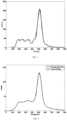
- FIG. 6 is a schematic diagram of the energy spectrum of the central scintillation crystal bar according to the nuclear detector of FIG. 1 .
- FIG. 7 is a schematic diagram of the energy spectrum of the peripheral scintillation crystal bar of the nuclear detector according to FIG. 1 .
- FIG. 8 is a schematic diagram of an average energy spectrum of the scintillation crystal bars according to the nuclear detector of FIG. 1 . As can be seen from FIG. 8 , an average energy resolution of the 13 ⁇ 13 scintillation crystal bars is 14.8%.
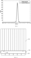
- FIG. 9 is a schematic diagram of the coincidence time resolution of the nuclear detector according to FIG. 1 .
- the statistics of 4573 pairs of adjacent lines of response (abbr. LOR, Line of Response) sampled in the SiPM-based nuclear detectors opposite to each other are consistent with the time distribution spectrum. All events are filtered through the energy window of 350-650keV.
- the coincidence time resolution obtained by means of Gaussian fitting is 941.4ps.
- FIG. 10 is a schematic front view of a nuclear detector according to another embodiment of the disclosure.
- the scintillation crystal array 110 and the photodetector array 130 of the nuclear detector are the same as those in the embodiment shown in FIG 1 , respectively, which thus will not be elaborated.
- the differences lie in that in the embodiment shown in FIG. 10 , provided in the top surface of the light guide 120 are only four first slits 122, which are cut parallel to the four sides of the top surface of the light guide 120, respectively.
- the slits 122 extend from the top surface of the light guide 120 toward inside of the light guide 120 in the thickness direction of the light guide 120.
- the four first slits 122 are spaced from the respective edges of the light guide 120 in a distance of 1.1-1.9 times the width of the scintillation crystal bar.
- the first slits 122 have a depth in a range of 0.1-0.5 times the thickness of the light guide 120.
- the first slits 120 are spaced from the respective edges of the corresponding light guide 120 in a distance of 1.5 times the width of the scintillation crystal bar.
- the first slits 122 have a depth of 0.4mm and the light guide 120 has a thickness of 1.4mm.
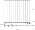
- FIG. 11 is a schematic front view of a nuclear detector according to an embodiment not covered by the claimed invention.
- the scintillation crystal array 210 and the photodetector array 230 of the nuclear detector are the same as those in the embodiment shown in FIG 1 , respectively, which thus will not be elaborated.
- the differences lie in that in the embodiment shown in FIG. 11 , the light guide 220 has a shape of truncated cone, including a top surface, an opposed bottom surface, and four side surfaces.
- the top surface area of the light guide 220 is greater than the bottom surface area, which is equal to the top surface area of the photodetector array 230.
- first slits 222 Provided in the top surface of the light guide 220 are four first slits 222 and four second slits 223.
- the planes where the first and second slits 222 and 223 are located are parallel to the four side surfaces of the light guide 220, respectively.
- the four first slits 222 are spaced from the respective side surfaces of the light guide 220 in a distance equal to the width of the single scintillation crystal bar, while the four second slits 223 are spaced from the respective side surfaces of the light guide 220 in a distance of two times the width of the single scintillation crystal bar.
- the first slits 222 have a depth greater than that of the second slits 223.
- the first slits 222 have a width of 0.2 mm and a depth of 1.0 mm
- the second slits 223 have a width of 0.2 mm and a depth of 0.4 mm.
- the material used for the light guide may be a transparent element such as ordinary inorganic glass, organic glass, or scintillation crystal.
- the light guide may comprise 2 to 4 layers, and the respective layers of light guide have a collective thickness in a range of 0.1 mm to 40 mm.
- the light guide may have a shape of a truncated circular cone, a cylinder, or a cone-like polyhedron.
- the width or diameter of the light guide may be in between the width of the scintillation crystal array and the width of the photodetector array.
- the opaque material filled in the first slits or the second slits of the light guide may also include a specular reflective film (aka. ESR, Enhanced Specular Reflector).
- a specular reflective film aka. ESR, Enhanced Specular Reflector
- the number of slits of the light guide may be greater than two, but no more than 40.
- the scintillation crystal bar may be an inorganic scintillation crystal, including bismuth germanate, lutetium oxyorthosilicate, lanthanum bromide, lutetium yttrium orthosilicate, lutetium oxyorthosilicate, barium fluoride, sodium iodide, cesium iodide or the like.
- the width of the single scintillation crystal bar in the scintillation crystal array is in a range of 0.5mm to 4mm.
- the photodetectors in the photodetector array may be further selected from any of avalanche photodiodes (APD), multi-pixel photon counters (MPPC), and Geiger avalanche photodiodes (G-APD).
- APD avalanche photodiodes
- MPPC multi-pixel photon counters
- G-APD Geiger avalanche photodiodes
- the scintillation crystal bars in the scintillation crystal array are significantly smaller than the photodetectors, that is, no 1: 1 direct coupling between the scintillation crystal bars and the photodetectors can be realized, arranged therebetween is a light guide with slits, enabling a nuclear detector with a high spatial resolution. Because of the relatively thin thickness of the light guide, there is little scintillation photon loss of the scintillation crystals, thus leading to little loss in the signal-to-noise ratio of the scintillation photon. Therefore, the high spatial resolution of the nuclear detector can be realized without compromising the performance of the nuclear detector, such that the energy resolution and the coincidence time resolution of the nuclear detector fulfills the needs of PET detector, which is easy to be produced or manufactured.
Landscapes
- Physics & Mathematics (AREA)
- Health & Medical Sciences (AREA)
- Spectroscopy & Molecular Physics (AREA)
- Life Sciences & Earth Sciences (AREA)
- General Physics & Mathematics (AREA)
- High Energy & Nuclear Physics (AREA)
- Molecular Biology (AREA)
- Crystallography & Structural Chemistry (AREA)
- Chemical & Material Sciences (AREA)
- Engineering & Computer Science (AREA)
- Biomedical Technology (AREA)
- General Health & Medical Sciences (AREA)
- Medical Informatics (AREA)
- Nuclear Medicine, Radiotherapy & Molecular Imaging (AREA)
- Optics & Photonics (AREA)
- Measurement Of Radiation (AREA)
- Nuclear Medicine (AREA)
Claims (10)
- Détecteur nucléaire, comprenant un réseau de cristaux de scintillation (10) comportant une pluralité de barres de cristal de scintillation (11) de la même taille disposées à la suite de façon rapprochée, un conduit de lumière (20), et un réseau de photodétecteurs (30) comportant une pluralité de photomultiplicateurs au silicium (SiPM) (31) disposés à la suite, dans lequel chacun des SiPM (31) a une aire de section transversale supérieure à une aire de section transversale de chacune des barres de cristal de scintillation (11), dans lequel le conduit de lumière (20) comporte une surface supérieure couplée au réseau de cristaux de scintillation (10), une surface inférieure opposée couplée à une surface supérieure du réseau de photodétecteurs (30), et une surface latérale ;le conduit de lumière (20) a une épaisseur dans une plage de 0,1 mm à 40 mm ;le conduit de lumière (20) comporte en outre une fente (22, 23, 122) adjacente à un bord du conduit de lumière (20), et la fente (22, 23, 122) est conçue pour s'étendre depuis la surface supérieure du conduit de lumière (20) vers la surface inférieure du conduit de lumière (20) et la fente (22, 23, 122) a une profondeur dans une plage de 0,1 à 0,5 fois l'épaisseur du conduit de lumière (20) ;le conduit de lumière (20) a une forme de cuboïde ;la fente (22, 23, 122) a une direction d'extension perpendiculaire à la surface supérieure et la surface inférieure du conduit de lumière (20) ; caractérisé en ce quela surface supérieure du réseau de photodétecteurs (30) a une aire inférieure à une aire de la surface inférieure du conduit de lumière (20) de telle sorte que le réseau de photodétecteurs (30) est en retrait au niveau de ses bords par rapport au conduit de lumière (20) et au réseau de cristaux de scintillation (10).
- Détecteur nucléaire selon la revendication 1, caractérisé en ce que la fente (22, 23, 122) est espacée de la surface latérale du conduit de lumière (20) d'une distance égale à 1,1 et 1,9 fois une largeur de la barre de cristal de scintillation (11).
- Détecteur nucléaire selon la revendication 1, caractérisé en ce que la fente (22, 23) comporte une première fente (22) espacée de la surface latérale du conduit de lumière (20) d'une distance égale à une largeur de la barre de cristal de scintillation (11), et une deuxième fente (23) espacée de la surface latérale du conduit de lumière (20) d'une distance égale à deux fois la largeur de la barre de cristal de scintillation (11), et la première fente (22) a une profondeur supérieure à une profondeur de la deuxième fente (23).
- Détecteur nucléaire selon l'une quelconque des revendications 1 à 3, caractérisé en ce qu'il y a un certain nombre de fentes et en ce que le nombre des fentes (22, 23, 122) se situe dans une plage de 1 à 40, et les fentes (22, 23, 122) sont disposées à la suite depuis la surface latérale du conduit de lumière (20) vers le centre du conduit de lumière (20), avec la profondeur des fentes (22, 23, 122) progressivement réduite depuis la surface latérale du conduit de lumière (20) vers le centre du conduit de lumière (20).
- Détecteur nucléaire selon l'une quelconque des revendications 1 à 4, caractérisé en ce que les barres de cristal de scintillation (11) ont une largeur dans une plage de 0,5 mm à 4 mm.
- Détecteur nucléaire selon l'une quelconque des revendications 1 à 5, caractérisé en ce que les barres de cristal de scintillation (11) ont une surface latérale revêtue d'un matériau opaque.
- Détecteur nucléaire selon la revendication 6, caractérisé en ce que le matériau opaque est de la poudre de sulfate de baryum ou un film de réflexion spéculaire.
- Détecteur nucléaire selon l'une quelconque des revendications 1 à 7, caractérisé en ce que la fente (22, 23, 122) et la surface latérale du conduit de lumière (20) sont revêtues d'un matériau opaque.
- Détecteur nucléaire selon la revendication 8, caractérisé en ce que le matériau opaque est une peinture noire.
- Détecteur nucléaire selon l'une quelconque des revendications 1 à 9, caractérisé en ce que le conduit de lumière (20) comprend 1 à 4 couches, et les couches respectives du conduit de lumière (20) ont une épaisseur collective dans une plage de 0,1 mm à 40 mm.
Applications Claiming Priority (2)
| Application Number | Priority Date | Filing Date | Title |
|---|---|---|---|
| CN201710631228.4A CN107167832A (zh) | 2017-07-28 | 2017-07-28 | 一种核探测器 |
| PCT/CN2017/108097 WO2019019449A1 (fr) | 2017-07-28 | 2017-10-27 | Détecteur de noyau |
Publications (3)
| Publication Number | Publication Date |
|---|---|
| EP3637148A1 EP3637148A1 (fr) | 2020-04-15 |
| EP3637148A4 EP3637148A4 (fr) | 2021-03-17 |
| EP3637148B1 true EP3637148B1 (fr) | 2025-02-19 |
Family
ID=59817568
Family Applications (1)
| Application Number | Title | Priority Date | Filing Date |
|---|---|---|---|
| EP17919078.0A Active EP3637148B1 (fr) | 2017-07-28 | 2017-10-27 | Détecteur de noyau |
Country Status (6)
| Country | Link |
|---|---|
| US (1) | US11194062B2 (fr) |
| EP (1) | EP3637148B1 (fr) |
| JP (1) | JP7224649B2 (fr) |
| CN (1) | CN107167832A (fr) |
| FI (1) | FI3637148T3 (fr) |
| WO (1) | WO2019019449A1 (fr) |
Families Citing this family (12)
| Publication number | Priority date | Publication date | Assignee | Title |
|---|---|---|---|---|
| CN107167832A (zh) * | 2017-07-28 | 2017-09-15 | 苏州瑞派宁科技有限公司 | 一种核探测器 |
| CN107728188B (zh) * | 2017-10-09 | 2019-08-16 | 山东麦德盈华科技有限公司 | 一种用于射线位置和能量测量的探测器和信号读出方法 |
| CN109765603A (zh) * | 2017-11-09 | 2019-05-17 | 苏州瑞派宁科技有限公司 | 一种光导及核探测器 |
| CN109856664B (zh) * | 2018-12-04 | 2020-12-01 | 山东麦德盈华科技有限公司 | 一种部分光导不切割的pet探测器 |
| CN109856665B (zh) | 2018-12-04 | 2020-12-01 | 山东麦德盈华科技有限公司 | 一种减少硅光电倍增管用量的pet探测器及探测方法 |
| CN109765599B (zh) * | 2018-12-11 | 2022-11-01 | 东软医疗系统股份有限公司 | 基于硅光电倍增管的探测器、机架和pet设备 |
| CN112641455B (zh) * | 2019-10-09 | 2024-06-18 | 安徽麦德盈华影像技术有限公司 | 一种头部渐窄型全身pet装置 |
| CN110764182B (zh) * | 2019-11-08 | 2021-03-02 | 江苏赛诺格兰医疗科技有限公司 | 一种用于闪烁体探测器的光导制作方法 |
| CN115153600B (zh) * | 2021-06-28 | 2026-04-21 | 湾影科技(深圳)有限公司 | 检测模块和具有该检测模块的发射成像设备 |
| CN114486950A (zh) * | 2022-01-14 | 2022-05-13 | 中国原子能科学研究院 | 射线成像方法和装置 |
| CN115220084B (zh) * | 2022-03-25 | 2024-12-24 | 北京滨松光子技术股份有限公司 | 一种闪烁晶体阵列、探测器、医疗影像设备及制作方法 |
| CN119509719A (zh) * | 2024-11-13 | 2025-02-25 | 上海理工大学 | 光子数可分辨探测系统及方法 |
Family Cites Families (18)
| Publication number | Priority date | Publication date | Assignee | Title |
|---|---|---|---|---|
| JPH0750596B2 (ja) * | 1988-12-05 | 1995-05-31 | 松下電器産業株式会社 | シンチレータ及びその光遮蔽膜の製造方法 |
| EP0958508B1 (fr) * | 1997-02-10 | 2007-03-28 | THE UNIVERSITY OF ALBERTA, SIMON FRASER UNIVERSITY, THE UNIV. OF VICTORIA,THE UNIV. OF BRITISH COLUMBIA, carrying on as TRIUMF | Detecteur de scintillation segmentee pour coordonnees d'interaction des photons |
| US7132664B1 (en) * | 2002-11-09 | 2006-11-07 | Crosetto Dario B | Method and apparatus for improving PET detectors |
| JP4110994B2 (ja) * | 2003-02-10 | 2008-07-02 | 株式会社島津製作所 | 放射線検出器 |
| JP2004354343A (ja) | 2003-05-30 | 2004-12-16 | Shimadzu Corp | 放射線検出器 |
| JP2004361303A (ja) * | 2003-06-06 | 2004-12-24 | Shimadzu Corp | 放射線検出器 |
| JP4525123B2 (ja) * | 2003-06-30 | 2010-08-18 | 株式会社島津製作所 | 放射線検出器およびその製造方法 |
| US7138638B2 (en) | 2003-11-20 | 2006-11-21 | Juni Jack E | Edge effects treatment for crystals |
| JP4305241B2 (ja) * | 2004-03-26 | 2009-07-29 | 株式会社島津製作所 | 放射線検出器 |
| US7573035B2 (en) | 2004-10-29 | 2009-08-11 | Koninklijke Philips Electronics N.V. | GOS ceramic scintillating fiber optics x-ray imaging plate for use in medical DF and RF imaging and in CT |
| US20130009066A1 (en) * | 2011-07-06 | 2013-01-10 | Siemens Aktiengesellschaft | Block Detector With Variable Microcell Size For Optimal Light Collection |
| EP2751597B1 (fr) * | 2011-10-12 | 2019-09-11 | Koninklijke Philips N.V. | Modélisation de matrices de détecteurs tof-doi |
| CN102879798B (zh) * | 2012-10-18 | 2016-01-06 | 中国科学院高能物理研究所 | 用于射线成像装置的闪烁探测器 |
| CN104049270B (zh) * | 2013-11-22 | 2017-02-08 | 沈阳东软医疗系统有限公司 | 一种光导及其制备方法、辐射探测器 |
| CN104237924B (zh) | 2014-08-20 | 2017-07-28 | 许剑锋 | 网格模具、包括该网格模具的检测器和发射成像设备 |
| CN105655435B (zh) * | 2014-11-14 | 2018-08-07 | 苏州瑞派宁科技有限公司 | 光电转换器、探测器及扫描设备 |
| CN105372693B (zh) | 2015-11-26 | 2019-07-16 | 东软医疗系统股份有限公司 | 一种晶体和光导的合成方法及模具 |
| CN107167832A (zh) * | 2017-07-28 | 2017-09-15 | 苏州瑞派宁科技有限公司 | 一种核探测器 |
-
2017
- 2017-07-28 CN CN201710631228.4A patent/CN107167832A/zh active Pending
- 2017-10-27 WO PCT/CN2017/108097 patent/WO2019019449A1/fr not_active Ceased
- 2017-10-27 FI FIEP17919078.0T patent/FI3637148T3/fi active
- 2017-10-27 US US16/623,038 patent/US11194062B2/en active Active
- 2017-10-27 JP JP2019568355A patent/JP7224649B2/ja active Active
- 2017-10-27 EP EP17919078.0A patent/EP3637148B1/fr active Active
Also Published As
| Publication number | Publication date |
|---|---|
| WO2019019449A1 (fr) | 2019-01-31 |
| CN107167832A (zh) | 2017-09-15 |
| EP3637148A1 (fr) | 2020-04-15 |
| US11194062B2 (en) | 2021-12-07 |
| EP3637148A4 (fr) | 2021-03-17 |
| FI3637148T3 (fi) | 2025-03-24 |
| JP7224649B2 (ja) | 2023-02-20 |
| US20200309969A1 (en) | 2020-10-01 |
| JP2020528137A (ja) | 2020-09-17 |
Similar Documents
| Publication | Publication Date | Title |
|---|---|---|
| EP3637148B1 (fr) | Détecteur de noyau | |
| Miyaoka et al. | Design of a depth of interaction (DOI) PET detector module | |
| Saoudi et al. | Investigation of depth-of-interaction by pulse shape discrimination in multicrystal detectors read out by avalanche photodiodes | |
| Zatcepin et al. | Detectors in positron emission tomography | |
| Kishimoto et al. | Development of a dual-sided readout DOI-PET module using large-area monolithic MPPC-arrays | |
| Cherry et al. | Optical fiber readout of scintillator arrays using a multi-channel PMT: a high resolution PET detector for animal imaging | |
| EP2399143B1 (fr) | Système de tomographie à émission de positrons / de résonance magnétique de gros calibre | |
| US10203419B2 (en) | Detector component for an X-ray or gamma ray detector | |
| Moses et al. | Factors influencing timing resolution in a commercial LSO PET camera | |
| USRE49174E1 (en) | Photosensors arranged on a surface of a scintillator | |
| US20150226862A1 (en) | Optical-interface patterning for radiation detector crystals | |
| US8946643B2 (en) | Virtual pixelated detector for pet and/or spect | |
| WO2016074560A1 (fr) | Convertisseur photoélectrique, détecteur et appareil de balayage | |
| Lewellen | The challenge of detector designs for PET | |
| US7381958B2 (en) | Lanthanum halide scintillators for time-of-flight 3-D pet | |
| CN109581460A (zh) | 复合探测装置 | |
| EP3236290A1 (fr) | Cristal de scintillation combiné, détecteur de scintillation combiné et dispositif de détection de rayonnement | |
| CN209400708U (zh) | 复合探测装置和系统 | |
| Vinke et al. | Optimization of digital time pickoff methods for LaBr 3-SiPM TOF-PET detectors | |
| CN207020321U (zh) | 一种核探测器 | |
| CN109407139B (zh) | 组合闪烁晶体及包括组合闪烁晶体的辐射探测装置和系统 | |
| Yamamoto et al. | Performance comparison of high quantum efficiency and normal quantum efficiency photomultiplier tubes and position sensitive photomultiplier tubes for high resolution PET and SPECT detectors | |
| Niu et al. | Design and measurement of Trans-PET basic detector module II using 6× 6 SiPM array for small-animal PET | |
| US20120085911A1 (en) | Tomographic imaging methods and systems for digital wave front decimation in time sampling | |
| US20190064367A1 (en) | Tileable block detectors for seamless block detector arrays in positron emission mammography |
Legal Events
| Date | Code | Title | Description |
|---|---|---|---|
| STAA | Information on the status of an ep patent application or granted ep patent |
Free format text: STATUS: THE INTERNATIONAL PUBLICATION HAS BEEN MADE |
|
| PUAI | Public reference made under article 153(3) epc to a published international application that has entered the european phase |
Free format text: ORIGINAL CODE: 0009012 |
|
| STAA | Information on the status of an ep patent application or granted ep patent |
Free format text: STATUS: REQUEST FOR EXAMINATION WAS MADE |
|
| 17P | Request for examination filed |
Effective date: 20200110 |
|
| AK | Designated contracting states |
Kind code of ref document: A1 Designated state(s): AL AT BE BG CH CY CZ DE DK EE ES FI FR GB GR HR HU IE IS IT LI LT LU LV MC MK MT NL NO PL PT RO RS SE SI SK SM TR |
|
| AX | Request for extension of the european patent |
Extension state: BA ME |
|
| DAV | Request for validation of the european patent (deleted) | ||
| DAX | Request for extension of the european patent (deleted) | ||
| A4 | Supplementary search report drawn up and despatched |
Effective date: 20210211 |
|
| RIC1 | Information provided on ipc code assigned before grant |
Ipc: G01T 1/202 20060101AFI20210205BHEP Ipc: G01T 1/164 20060101ALI20210205BHEP Ipc: G01T 1/29 20060101ALI20210205BHEP Ipc: G01T 1/20 20060101ALI20210205BHEP |
|
| RIN1 | Information on inventor provided before grant (corrected) |
Inventor name: XIE, QINGGUO Inventor name: SUN, YICHENG Inventor name: HUA, YUEXUAN Inventor name: LIU, TONG Inventor name: NIU, MING |
|
| STAA | Information on the status of an ep patent application or granted ep patent |
Free format text: STATUS: EXAMINATION IS IN PROGRESS |
|
| 17Q | First examination report despatched |
Effective date: 20221108 |
|
| GRAP | Despatch of communication of intention to grant a patent |
Free format text: ORIGINAL CODE: EPIDOSNIGR1 |
|
| STAA | Information on the status of an ep patent application or granted ep patent |
Free format text: STATUS: GRANT OF PATENT IS INTENDED |
|
| INTG | Intention to grant announced |
Effective date: 20240920 |
|
| GRAS | Grant fee paid |
Free format text: ORIGINAL CODE: EPIDOSNIGR3 |
|
| GRAA | (expected) grant |
Free format text: ORIGINAL CODE: 0009210 |
|
| STAA | Information on the status of an ep patent application or granted ep patent |
Free format text: STATUS: THE PATENT HAS BEEN GRANTED |
|
| AK | Designated contracting states |
Kind code of ref document: B1 Designated state(s): AL AT BE BG CH CY CZ DE DK EE ES FI FR GB GR HR HU IE IS IT LI LT LU LV MC MK MT NL NO PL PT RO RS SE SI SK SM TR |
|
| REG | Reference to a national code |
Ref country code: GB Ref legal event code: FG4D |
|
| REG | Reference to a national code |
Ref country code: CH Ref legal event code: EP |
|
| REG | Reference to a national code |
Ref country code: IE Ref legal event code: FG4D |
|
| REG | Reference to a national code |
Ref country code: DE Ref legal event code: R096 Ref document number: 602017087946 Country of ref document: DE |
|
| REG | Reference to a national code |
Ref country code: FI Ref legal event code: FGE |
|
| REG | Reference to a national code |
Ref country code: NL Ref legal event code: MP Effective date: 20250219 |
|
| PG25 | Lapsed in a contracting state [announced via postgrant information from national office to epo] |
Ref country code: RS Free format text: LAPSE BECAUSE OF FAILURE TO SUBMIT A TRANSLATION OF THE DESCRIPTION OR TO PAY THE FEE WITHIN THE PRESCRIBED TIME-LIMIT Effective date: 20250519 |
|
| PG25 | Lapsed in a contracting state [announced via postgrant information from national office to epo] |
Ref country code: PL Free format text: LAPSE BECAUSE OF FAILURE TO SUBMIT A TRANSLATION OF THE DESCRIPTION OR TO PAY THE FEE WITHIN THE PRESCRIBED TIME-LIMIT Effective date: 20250219 |
|
| PG25 | Lapsed in a contracting state [announced via postgrant information from national office to epo] |
Ref country code: ES Free format text: LAPSE BECAUSE OF FAILURE TO SUBMIT A TRANSLATION OF THE DESCRIPTION OR TO PAY THE FEE WITHIN THE PRESCRIBED TIME-LIMIT Effective date: 20250219 |
|
| REG | Reference to a national code |
Ref country code: LT Ref legal event code: MG9D |
|
| PG25 | Lapsed in a contracting state [announced via postgrant information from national office to epo] |
Ref country code: IS Free format text: LAPSE BECAUSE OF FAILURE TO SUBMIT A TRANSLATION OF THE DESCRIPTION OR TO PAY THE FEE WITHIN THE PRESCRIBED TIME-LIMIT Effective date: 20250619 Ref country code: NO Free format text: LAPSE BECAUSE OF FAILURE TO SUBMIT A TRANSLATION OF THE DESCRIPTION OR TO PAY THE FEE WITHIN THE PRESCRIBED TIME-LIMIT Effective date: 20250519 |
|
| PG25 | Lapsed in a contracting state [announced via postgrant information from national office to epo] |
Ref country code: NL Free format text: LAPSE BECAUSE OF FAILURE TO SUBMIT A TRANSLATION OF THE DESCRIPTION OR TO PAY THE FEE WITHIN THE PRESCRIBED TIME-LIMIT Effective date: 20250219 |
|
| PG25 | Lapsed in a contracting state [announced via postgrant information from national office to epo] |
Ref country code: HR Free format text: LAPSE BECAUSE OF FAILURE TO SUBMIT A TRANSLATION OF THE DESCRIPTION OR TO PAY THE FEE WITHIN THE PRESCRIBED TIME-LIMIT Effective date: 20250219 |
|
| PG25 | Lapsed in a contracting state [announced via postgrant information from national office to epo] |
Ref country code: PT Free format text: LAPSE BECAUSE OF FAILURE TO SUBMIT A TRANSLATION OF THE DESCRIPTION OR TO PAY THE FEE WITHIN THE PRESCRIBED TIME-LIMIT Effective date: 20250620 Ref country code: LV Free format text: LAPSE BECAUSE OF FAILURE TO SUBMIT A TRANSLATION OF THE DESCRIPTION OR TO PAY THE FEE WITHIN THE PRESCRIBED TIME-LIMIT Effective date: 20250219 |
|
| PG25 | Lapsed in a contracting state [announced via postgrant information from national office to epo] |
Ref country code: GR Free format text: LAPSE BECAUSE OF FAILURE TO SUBMIT A TRANSLATION OF THE DESCRIPTION OR TO PAY THE FEE WITHIN THE PRESCRIBED TIME-LIMIT Effective date: 20250520 Ref country code: BG Free format text: LAPSE BECAUSE OF FAILURE TO SUBMIT A TRANSLATION OF THE DESCRIPTION OR TO PAY THE FEE WITHIN THE PRESCRIBED TIME-LIMIT Effective date: 20250219 |
|
| REG | Reference to a national code |
Ref country code: AT Ref legal event code: MK05 Ref document number: 1768775 Country of ref document: AT Kind code of ref document: T Effective date: 20250219 |
|
| PG25 | Lapsed in a contracting state [announced via postgrant information from national office to epo] |
Ref country code: SE Free format text: LAPSE BECAUSE OF FAILURE TO SUBMIT A TRANSLATION OF THE DESCRIPTION OR TO PAY THE FEE WITHIN THE PRESCRIBED TIME-LIMIT Effective date: 20250219 |
|
| PG25 | Lapsed in a contracting state [announced via postgrant information from national office to epo] |
Ref country code: SM Free format text: LAPSE BECAUSE OF FAILURE TO SUBMIT A TRANSLATION OF THE DESCRIPTION OR TO PAY THE FEE WITHIN THE PRESCRIBED TIME-LIMIT Effective date: 20250219 |
|
| PGFP | Annual fee paid to national office [announced via postgrant information from national office to epo] |
Ref country code: FI Payment date: 20250922 Year of fee payment: 9 |
|
| PG25 | Lapsed in a contracting state [announced via postgrant information from national office to epo] |
Ref country code: DK Free format text: LAPSE BECAUSE OF FAILURE TO SUBMIT A TRANSLATION OF THE DESCRIPTION OR TO PAY THE FEE WITHIN THE PRESCRIBED TIME-LIMIT Effective date: 20250219 |
|
| PG25 | Lapsed in a contracting state [announced via postgrant information from national office to epo] |
Ref country code: AT Free format text: LAPSE BECAUSE OF FAILURE TO SUBMIT A TRANSLATION OF THE DESCRIPTION OR TO PAY THE FEE WITHIN THE PRESCRIBED TIME-LIMIT Effective date: 20250219 |
|
| PG25 | Lapsed in a contracting state [announced via postgrant information from national office to epo] |
Ref country code: EE Free format text: LAPSE BECAUSE OF FAILURE TO SUBMIT A TRANSLATION OF THE DESCRIPTION OR TO PAY THE FEE WITHIN THE PRESCRIBED TIME-LIMIT Effective date: 20250219 Ref country code: CZ Free format text: LAPSE BECAUSE OF FAILURE TO SUBMIT A TRANSLATION OF THE DESCRIPTION OR TO PAY THE FEE WITHIN THE PRESCRIBED TIME-LIMIT Effective date: 20250219 |
|
| PG25 | Lapsed in a contracting state [announced via postgrant information from national office to epo] |
Ref country code: RO Free format text: LAPSE BECAUSE OF FAILURE TO SUBMIT A TRANSLATION OF THE DESCRIPTION OR TO PAY THE FEE WITHIN THE PRESCRIBED TIME-LIMIT Effective date: 20250219 |
|
| PG25 | Lapsed in a contracting state [announced via postgrant information from national office to epo] |
Ref country code: SK Free format text: LAPSE BECAUSE OF FAILURE TO SUBMIT A TRANSLATION OF THE DESCRIPTION OR TO PAY THE FEE WITHIN THE PRESCRIBED TIME-LIMIT Effective date: 20250219 |
|
| REG | Reference to a national code |
Ref country code: DE Ref legal event code: R097 Ref document number: 602017087946 Country of ref document: DE |
|
| PLBE | No opposition filed within time limit |
Free format text: ORIGINAL CODE: 0009261 |
|
| STAA | Information on the status of an ep patent application or granted ep patent |
Free format text: STATUS: NO OPPOSITION FILED WITHIN TIME LIMIT |
|
| PGFP | Annual fee paid to national office [announced via postgrant information from national office to epo] |
Ref country code: DE Payment date: 20251015 Year of fee payment: 9 |
|
| PGFP | Annual fee paid to national office [announced via postgrant information from national office to epo] |
Ref country code: IT Payment date: 20251007 Year of fee payment: 9 |
|
| PGFP | Annual fee paid to national office [announced via postgrant information from national office to epo] |
Ref country code: FR Payment date: 20251027 Year of fee payment: 9 |
|
| 26N | No opposition filed |
Effective date: 20251120 |