EP3637405B1 - Pixelschaltung und ansteuerungsverfahren dafür sowie anzeigetafel - Google Patents
Pixelschaltung und ansteuerungsverfahren dafür sowie anzeigetafel Download PDFInfo
- Publication number
- EP3637405B1 EP3637405B1 EP18814246.7A EP18814246A EP3637405B1 EP 3637405 B1 EP3637405 B1 EP 3637405B1 EP 18814246 A EP18814246 A EP 18814246A EP 3637405 B1 EP3637405 B1 EP 3637405B1
- Authority
- EP
- European Patent Office
- Prior art keywords
- voltage
- transistor
- node
- scanning signal
- gate
- Prior art date
- Legal status (The legal status is an assumption and is not a legal conclusion. Google has not performed a legal analysis and makes no representation as to the accuracy of the status listed.)
- Active
Links
Images
Classifications
-
- G—PHYSICS
- G09—EDUCATION; CRYPTOGRAPHY; DISPLAY; ADVERTISING; SEALS
- G09G—ARRANGEMENTS OR CIRCUITS FOR CONTROL OF INDICATING DEVICES USING STATIC MEANS TO PRESENT VARIABLE INFORMATION
- G09G3/00—Control arrangements or circuits, of interest only in connection with visual indicators other than cathode-ray tubes
- G09G3/20—Control arrangements or circuits, of interest only in connection with visual indicators other than cathode-ray tubes for presentation of an assembly of a number of characters, e.g. a page, by composing the assembly by combination of individual elements arranged in a matrix no fixed position being assigned to or needed to be assigned to the individual characters or partial characters
- G09G3/22—Control arrangements or circuits, of interest only in connection with visual indicators other than cathode-ray tubes for presentation of an assembly of a number of characters, e.g. a page, by composing the assembly by combination of individual elements arranged in a matrix no fixed position being assigned to or needed to be assigned to the individual characters or partial characters using controlled light sources
- G09G3/30—Control arrangements or circuits, of interest only in connection with visual indicators other than cathode-ray tubes for presentation of an assembly of a number of characters, e.g. a page, by composing the assembly by combination of individual elements arranged in a matrix no fixed position being assigned to or needed to be assigned to the individual characters or partial characters using controlled light sources using electroluminescent panels
- G09G3/32—Control arrangements or circuits, of interest only in connection with visual indicators other than cathode-ray tubes for presentation of an assembly of a number of characters, e.g. a page, by composing the assembly by combination of individual elements arranged in a matrix no fixed position being assigned to or needed to be assigned to the individual characters or partial characters using controlled light sources using electroluminescent panels semiconductive, e.g. using light-emitting diodes [LED]
- G09G3/3208—Control arrangements or circuits, of interest only in connection with visual indicators other than cathode-ray tubes for presentation of an assembly of a number of characters, e.g. a page, by composing the assembly by combination of individual elements arranged in a matrix no fixed position being assigned to or needed to be assigned to the individual characters or partial characters using controlled light sources using electroluminescent panels semiconductive, e.g. using light-emitting diodes [LED] organic, e.g. using organic light-emitting diodes [OLED]
- G09G3/3225—Control arrangements or circuits, of interest only in connection with visual indicators other than cathode-ray tubes for presentation of an assembly of a number of characters, e.g. a page, by composing the assembly by combination of individual elements arranged in a matrix no fixed position being assigned to or needed to be assigned to the individual characters or partial characters using controlled light sources using electroluminescent panels semiconductive, e.g. using light-emitting diodes [LED] organic, e.g. using organic light-emitting diodes [OLED] using an active matrix
- G09G3/3233—Control arrangements or circuits, of interest only in connection with visual indicators other than cathode-ray tubes for presentation of an assembly of a number of characters, e.g. a page, by composing the assembly by combination of individual elements arranged in a matrix no fixed position being assigned to or needed to be assigned to the individual characters or partial characters using controlled light sources using electroluminescent panels semiconductive, e.g. using light-emitting diodes [LED] organic, e.g. using organic light-emitting diodes [OLED] using an active matrix with pixel circuitry controlling the current through the light-emitting element
-
- G—PHYSICS
- G09—EDUCATION; CRYPTOGRAPHY; DISPLAY; ADVERTISING; SEALS
- G09G—ARRANGEMENTS OR CIRCUITS FOR CONTROL OF INDICATING DEVICES USING STATIC MEANS TO PRESENT VARIABLE INFORMATION
- G09G3/00—Control arrangements or circuits, of interest only in connection with visual indicators other than cathode-ray tubes
- G09G3/20—Control arrangements or circuits, of interest only in connection with visual indicators other than cathode-ray tubes for presentation of an assembly of a number of characters, e.g. a page, by composing the assembly by combination of individual elements arranged in a matrix no fixed position being assigned to or needed to be assigned to the individual characters or partial characters
- G09G3/22—Control arrangements or circuits, of interest only in connection with visual indicators other than cathode-ray tubes for presentation of an assembly of a number of characters, e.g. a page, by composing the assembly by combination of individual elements arranged in a matrix no fixed position being assigned to or needed to be assigned to the individual characters or partial characters using controlled light sources
- G09G3/30—Control arrangements or circuits, of interest only in connection with visual indicators other than cathode-ray tubes for presentation of an assembly of a number of characters, e.g. a page, by composing the assembly by combination of individual elements arranged in a matrix no fixed position being assigned to or needed to be assigned to the individual characters or partial characters using controlled light sources using electroluminescent panels
- G09G3/32—Control arrangements or circuits, of interest only in connection with visual indicators other than cathode-ray tubes for presentation of an assembly of a number of characters, e.g. a page, by composing the assembly by combination of individual elements arranged in a matrix no fixed position being assigned to or needed to be assigned to the individual characters or partial characters using controlled light sources using electroluminescent panels semiconductive, e.g. using light-emitting diodes [LED]
- G09G3/3208—Control arrangements or circuits, of interest only in connection with visual indicators other than cathode-ray tubes for presentation of an assembly of a number of characters, e.g. a page, by composing the assembly by combination of individual elements arranged in a matrix no fixed position being assigned to or needed to be assigned to the individual characters or partial characters using controlled light sources using electroluminescent panels semiconductive, e.g. using light-emitting diodes [LED] organic, e.g. using organic light-emitting diodes [OLED]
- G09G3/3225—Control arrangements or circuits, of interest only in connection with visual indicators other than cathode-ray tubes for presentation of an assembly of a number of characters, e.g. a page, by composing the assembly by combination of individual elements arranged in a matrix no fixed position being assigned to or needed to be assigned to the individual characters or partial characters using controlled light sources using electroluminescent panels semiconductive, e.g. using light-emitting diodes [LED] organic, e.g. using organic light-emitting diodes [OLED] using an active matrix
- G09G3/3258—Control arrangements or circuits, of interest only in connection with visual indicators other than cathode-ray tubes for presentation of an assembly of a number of characters, e.g. a page, by composing the assembly by combination of individual elements arranged in a matrix no fixed position being assigned to or needed to be assigned to the individual characters or partial characters using controlled light sources using electroluminescent panels semiconductive, e.g. using light-emitting diodes [LED] organic, e.g. using organic light-emitting diodes [OLED] using an active matrix with pixel circuitry controlling the voltage across the light-emitting element
-
- G—PHYSICS
- G09—EDUCATION; CRYPTOGRAPHY; DISPLAY; ADVERTISING; SEALS
- G09G—ARRANGEMENTS OR CIRCUITS FOR CONTROL OF INDICATING DEVICES USING STATIC MEANS TO PRESENT VARIABLE INFORMATION
- G09G2300/00—Aspects of the constitution of display devices
- G09G2300/04—Structural and physical details of display devices
- G09G2300/0421—Structural details of the set of electrodes
- G09G2300/0426—Layout of electrodes and connections
-
- G—PHYSICS
- G09—EDUCATION; CRYPTOGRAPHY; DISPLAY; ADVERTISING; SEALS
- G09G—ARRANGEMENTS OR CIRCUITS FOR CONTROL OF INDICATING DEVICES USING STATIC MEANS TO PRESENT VARIABLE INFORMATION
- G09G2300/00—Aspects of the constitution of display devices
- G09G2300/04—Structural and physical details of display devices
- G09G2300/0439—Pixel structures
- G09G2300/0465—Improved aperture ratio, e.g. by size reduction of the pixel circuit, e.g. for improving the pixel density or the maximum displayable luminance or brightness
-
- G—PHYSICS
- G09—EDUCATION; CRYPTOGRAPHY; DISPLAY; ADVERTISING; SEALS
- G09G—ARRANGEMENTS OR CIRCUITS FOR CONTROL OF INDICATING DEVICES USING STATIC MEANS TO PRESENT VARIABLE INFORMATION
- G09G2300/00—Aspects of the constitution of display devices
- G09G2300/08—Active matrix structure, i.e. with use of active elements, inclusive of non-linear two terminal elements, in the pixels together with light emitting or modulating elements
- G09G2300/0809—Several active elements per pixel in active matrix panels
- G09G2300/0819—Several active elements per pixel in active matrix panels used for counteracting undesired variations, e.g. feedback or autozeroing
-
- G—PHYSICS
- G09—EDUCATION; CRYPTOGRAPHY; DISPLAY; ADVERTISING; SEALS
- G09G—ARRANGEMENTS OR CIRCUITS FOR CONTROL OF INDICATING DEVICES USING STATIC MEANS TO PRESENT VARIABLE INFORMATION
- G09G2300/00—Aspects of the constitution of display devices
- G09G2300/08—Active matrix structure, i.e. with use of active elements, inclusive of non-linear two terminal elements, in the pixels together with light emitting or modulating elements
- G09G2300/0809—Several active elements per pixel in active matrix panels
- G09G2300/0842—Several active elements per pixel in active matrix panels forming a memory circuit, e.g. a dynamic memory with one capacitor
-
- G—PHYSICS
- G09—EDUCATION; CRYPTOGRAPHY; DISPLAY; ADVERTISING; SEALS
- G09G—ARRANGEMENTS OR CIRCUITS FOR CONTROL OF INDICATING DEVICES USING STATIC MEANS TO PRESENT VARIABLE INFORMATION
- G09G2300/00—Aspects of the constitution of display devices
- G09G2300/08—Active matrix structure, i.e. with use of active elements, inclusive of non-linear two terminal elements, in the pixels together with light emitting or modulating elements
- G09G2300/0809—Several active elements per pixel in active matrix panels
- G09G2300/0842—Several active elements per pixel in active matrix panels forming a memory circuit, e.g. a dynamic memory with one capacitor
- G09G2300/0861—Several active elements per pixel in active matrix panels forming a memory circuit, e.g. a dynamic memory with one capacitor with additional control of the display period without amending the charge stored in a pixel memory, e.g. by means of additional select electrodes
-
- G—PHYSICS
- G09—EDUCATION; CRYPTOGRAPHY; DISPLAY; ADVERTISING; SEALS
- G09G—ARRANGEMENTS OR CIRCUITS FOR CONTROL OF INDICATING DEVICES USING STATIC MEANS TO PRESENT VARIABLE INFORMATION
- G09G2310/00—Command of the display device
- G09G2310/02—Addressing, scanning or driving the display screen or processing steps related thereto
- G09G2310/0264—Details of driving circuits
- G09G2310/0286—Details of a shift registers arranged for use in a driving circuit
-
- G—PHYSICS
- G09—EDUCATION; CRYPTOGRAPHY; DISPLAY; ADVERTISING; SEALS
- G09G—ARRANGEMENTS OR CIRCUITS FOR CONTROL OF INDICATING DEVICES USING STATIC MEANS TO PRESENT VARIABLE INFORMATION
- G09G2310/00—Command of the display device
- G09G2310/08—Details of timing specific for flat panels, other than clock recovery
-
- G—PHYSICS
- G09—EDUCATION; CRYPTOGRAPHY; DISPLAY; ADVERTISING; SEALS
- G09G—ARRANGEMENTS OR CIRCUITS FOR CONTROL OF INDICATING DEVICES USING STATIC MEANS TO PRESENT VARIABLE INFORMATION
- G09G2320/00—Control of display operating conditions
- G09G2320/02—Improving the quality of display appearance
- G09G2320/0223—Compensation for problems related to R-C delay and attenuation in electrodes of matrix panels, e.g. in gate electrodes or on-substrate video signal electrodes
-
- G—PHYSICS
- G09—EDUCATION; CRYPTOGRAPHY; DISPLAY; ADVERTISING; SEALS
- G09G—ARRANGEMENTS OR CIRCUITS FOR CONTROL OF INDICATING DEVICES USING STATIC MEANS TO PRESENT VARIABLE INFORMATION
- G09G2320/00—Control of display operating conditions
- G09G2320/02—Improving the quality of display appearance
- G09G2320/0233—Improving the luminance or brightness uniformity across the screen
-
- G—PHYSICS
- G09—EDUCATION; CRYPTOGRAPHY; DISPLAY; ADVERTISING; SEALS
- G09G—ARRANGEMENTS OR CIRCUITS FOR CONTROL OF INDICATING DEVICES USING STATIC MEANS TO PRESENT VARIABLE INFORMATION
- G09G2320/00—Control of display operating conditions
- G09G2320/02—Improving the quality of display appearance
- G09G2320/0238—Improving the black level
Definitions
- the present disclosure relates to the field of display technologies, and in particular, to a pixel circuit and a method of driving the same, and a display panel.
- OLED organic light-emitting display
- LTPS low temperature polysilicon
- US2017270860A1 discloses a pixel circuit, a drive method thereof, and a related device, comprising: a first reset module, a data write module, a compensation module, a voltage stabilization module, a drive control module, a light emission control module and a light emission component.
- the pixel circuit can compensate for the drift of the threshold voltage of the drive control module by the cooperation of the above-described modules.
- US2011273419A1 discloses a pixel circuit of a flat panel display device and a method for driving thereof.
- the pixel circuit includes a first transistor having a first gate electrode coupled to a scan line, a second electrode coupled to a data line, a second gate electrode coupled to a controlling signal line, and a first electrode, a second transistor having a first gate electrode coupled to the first electrode of the first transistor, a second electrode coupled to a first voltage source, a second gate electrode coupled to the controlling signal line, and a first electrode, a capacitor coupled between the first gate electrode of the second transistor and the first electrode of the second transistor, and an organic light emitting diode coupled between the first electrode of the second transistor and a second voltage source, in which the threshold voltage of the first and second transistors may be controlled to the required level by supplying a controlling signal of a fixed voltage level to the second gate electrodes of the first and second transistors through the controlling signal line
- the present disclosure provides a pixel circuit which is defined by appended claim 1.
- the present disclosure provides a method of driving a pixel circuit which is defined be appended claim 5.
- the present disclosure provides a display panel which is defined by appended claim 6.
- Transistors used in all embodiments of the present disclosure may be thin film transistors or field-effect transistors or other devices having the same properties.
- the transistors used in embodiments of the present disclosure mainly include switching transistors and driving transistors depending on functions of the transistors in the circuit. Since a source and a drain of a switching transistor used herein are symmetrical, the source and the drain are interchangeable.
- one electrode is referred to as a source, and another electrode is referred to as a drain.
- a middle terminal of the transistor is defined as a gate
- a signal input terminal of the transistor is defined as a source
- a signal output terminal of the transistor is defined as a drain.
- the switching transistors used in embodiments of the present disclosure include P-type switching transistors and N-type switching transistors.
- a P-type switching transistor is turned on when the gate is at a low level, and is cut off when the gate is at a high level.
- An N-type switching transistor is turned on when the gate is at a high level, and is cut off when the gate is at a low level.
- the driving transistors include P-type driving transistors and N-type driving transistors.
- a P-type driving transistor is in an amplified state or a saturated state when a gate voltage on a gate of the P-type driving transistor is at a low level (the gate voltage is smaller than a source voltage) and an absolute value of a difference between the gate voltage and the source voltage is greater than a threshold voltage.
- the N-type driving transistor is in an amplified state or a saturated state when a gate voltage on a gate of the N-type driving transistor is at a high level (the gate voltage is greater than a source voltage) and an absolute value of a difference between the gate voltage and the source voltage is greater than a threshold voltage.
- an allocated read time for the threshold voltage of the DTFT of each pixel is continuously shortened.
- the read time of the threshold voltage of the DTFT of each pixel is less than 5 ⁇ s, and the higher the resolution, the shorter the read time of the threshold voltage of the DTFT of each pixel. Since the allocated read time for the threshold voltage of the DTFT of each pixel is continuously shortened, a pixel circuit may not be able to read the threshold voltage of the DTFT, which may result in uneven display and mura.
- Embodiments of the present disclosure provide a pixel circuit.
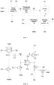
- the pixel circuit includes a node control circuit 11, a driver 12, a display sub-circuit 13, a threshold compensator 14, and a reset device 15.
- the node control circuit 11 is configured to receive a first scanning signal S1, a second scanning signal S2, a third scanning signal S3, a reference voltage Vref and a data voltage Vdata.
- the node control circuit 11 is further configured to output the reference voltage Vref to a first node N1 under the control of a voltage of the first scanning signal S1 or a voltage of the second scanning signal S2, or to output the data voltage Vdata to the first node N1 under the control of a voltage of the third scanning signal S3.
- the driver 12 is configured to receive a first level signal V1 at its input terminal I, and a control terminal Q of the driver 12 is coupled to a second node N2.
- the driver 12 is further configured to output a driving current at an output terminal O of the driver 12 under the control of a voltage of the first level signal V1 and a voltage of the second node N2.
- the display sub-circuit 13 is coupled to the reset device 15 and the output terminal O of the driver 12.
- the display sub-circuit 13 is configured to receive a second level signal V2 and the second scanning signal S2.
- the display sub-circuit 13 is further configured to display a gray-scale by the driving current under the control of the voltage of the second scanning signal S2.
- the threshold compensator 14 is coupled to the first node N1, the output terminal O of driver 12, and the second node N2.
- the threshold compensator 14 is configured to receive the third scanning signal S3 and a fourth scanning signal S4.
- the threshold compensator 14 is further configured to adjust the voltage of the second node N2 to a sum of the voltage of the first level signal V1 and a threshold voltage of the driver 12 under the control of the voltage of the third scanning signal S3 or a voltage of the fourth scanning signal S4, and to adjust the voltage of the second node N2 to a difference between a sum of the voltage of the first level signal V1, the threshold voltage of the driver 12 and the reference voltage Vref, and the data voltage Vdata under the control of a voltage of the first node N1 and a voltage of the output terminal O of the driver 12.
- the reset device 15 is coupled to the second node N2 and the display sub-circuit 13.
- the reset device 15 is configured to receive a reset voltage signal Vinit, the first scanning signal S1 and the third scanning signal S3.
- the reset device 15 is further configured to reset the second node N2 by a voltage of the reset voltage signal Vinit under the control of the voltage of the first scanning signal S1, and to reset the display sub-circuit 13 by means of the voltage of the reset voltage signal Vinit under the control of the voltage of the third scanning signal S3.
- the first node N1 is an intersection of an output of the node control circuit 11 and an input of the threshold compensator 14.
- the second node N2 is an intersection of an output of the threshold compensator 14, an input of the driver 12, and an output of the reset device 15.
- the pixel circuit provided by the embodiments of the present disclosure includes the node control circuit 11, the threshold compensator 14, the reset device 15, the driver 12, and the display sub-circuit 13.
- the threshold compensator 14 may adjust the voltage of the second node N2 to the sum of the voltage of the first level signal V1 and the threshold voltage of the driver 12 under the control of the voltage of the third scanning signal S3 or the voltage of the fourth scanning signal S4, that is, the pixel circuit provided by the embodiments of the present disclosure may read the threshold voltage of the driver 12 when the third scanning signal or the fourth scanning signal is an effective signal. Therefore, the pixel circuit provided by the embodiments of the present disclosure may increase a length of time that the pixel circuit reads the threshold voltage of the driver, thereby solving a problem that the pixel circuit cannot read the threshold voltage of the driver.
- Embodiments of the present application further provide a specific circuit structure of the pixel circuit shown in FIG.1 .
- the node control circuit 11 includes a first transistor T1, a second transistor T2, and a third transistor T3.
- the first transistor T1 is configured to receive the reference voltage Vref at a first electrode of the first transistor, a second electrode of the first transistor T1 is coupled to the first node N1, and the first transistor T1 is configured to receive the first scanning signal S1 at a gate of the first transistor.
- the second transistor T2 is configured to receive the reference voltage Vref at a first electrode of the second transistor, a second electrode of the second transistor T2 is coupled to the first node N1, and the second transistor T2 is configured to receive the second scanning signal S2 at a gate of the second transistor.
- the third transistor T3 is configured to receive the data voltage Vdata at a first electrode of the third transistor, a second electrode of the third transistor T3 is coupled to the first node N1, and the third transistor T3 is configured to receive the third scanning signal S3 at a gate of the third transistor.
- the threshold compensator 14 includes a fourth transistor T4, a fifth transistor T5, and a first capacitor C1.
- a first electrode of the fourth transistor T4 is coupled to the output terminal O of the driver 12, a second electrode of the fourth transistor T4 is coupled to the second node N2, and the fourth transistor T4 is configured to receive the third scanning signal S3 at a gate of the fourth transistor.
- a first electrode of the fifth transistor T5 is coupled to the output terminal O of the driver 12, a second electrode of the fifth transistor T5 is coupled to the second node N2, and the fifth transistor T5 is configured to receive the fourth scanning signal S4 at a gate of the fifth transistor.
- a first electrode of the first capacitor C1 is coupled to the first node N1, and a second electrode of the first capacitor C1 is coupled to the second node N2.
- the reset device 15 includes a sixth transistor T6 and a seventh transistor T7.
- the sixth transistor T6 is configured to receive the reset voltage signal Vinit at a first electrode of the sixth transistor, a second electrode of the sixth transistor T6 is coupled to the second node N2, and the sixth transistor T6 is configured to receive the first scanning signal S1 at a gate of the sixth transistor.
- the seventh transistor T7 is configured to receive the reset voltage signal Vinit at a first electrode of the seventh transistor, a second electrode of the seventh transistor T7 is coupled to the display sub-circuit 13, and the seventh transistor T7 is configured to receive the third scanning signal S3 at a gate of the seventh transistor.
- the driver 12 is a DTFT, and the input terminal I of the driver 12 is a source of the DTFT, the control terminal Q of the driver 12 is a gate of the DTFT, and the output terminal O of the driver 12 is a drain of the DTFT.
- the display sub-circuit 13 includes an eighth transistor T8 and a light-emitting diode D1.
- a first electrode of the eighth transistor T8 is coupled to the output terminal O of the driver 12, a second electrode of the eighth transistor T8 is coupled to an anode of the light-emitting diode D1, and the eighth transistor T8 is configured to receive the second scanning signal S2 at a gate of the eighth transistor.
- the light-emitting diode D1 is configured to receive the second level signal V2 at a cathode of the light-emitting diode.
- Embodiments of the present disclosure further provide a method of driving the pixel circuit described above. Specifically, referring to FIG.3 , the method includes the following steps.
- the node control circuit outputs the reference voltage to the first node under the control of the voltage of the first scanning signal; and the reset device resets the second node by means of the voltage of the reset voltage signal under the control of the voltage of the first scanning signal.
- the node control circuit outputs the data voltage to the first node under the control of the voltage of the third scanning signal; the threshold compensator adjusts the voltage of the second node to the sum of the voltage of the first level signal and the threshold voltage of the driver; and a reset device resets the display sub-circuit by the voltage of the reset voltage signal under the control of the voltage of the third scanning signal.
- the threshold compensator adjusts the voltage of the second node to the sum of the voltage of the first level signal and the threshold voltage of the driver under the control of the voltage of the fourth scanning signal.
- the node control circuit outputs the reference voltage to the first node under the control of the voltage of the second scanning signal; the threshold compensator adjusts the voltage of the second node to the difference between the sum of the voltage of the first level signal, the threshold voltage of the driver and the reference voltage, and the data voltage under the control of the voltage of the first node and the voltage of the output terminal of the driver; the driver outputs the driving current at the output term inal of the driver under the control of the voltage of the first level signal and the voltage of the second node; and the display sub-circuit displays a gray-scale by the driving current under the control of the voltage of the second scanning signal.
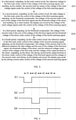
- FIG.4 includes signal timing states of the first scanning signal S1, the second scanning signal S2, the third scanning signal S3, and the fourth scanning signal S4.
- the first level signal V1 provides a high level Vdd
- the second level signal V2 is grounded to provide Vss.
- the second level signal V2 may be grounded.
- t1 a first period
- t2 a second period
- t3 a third period
- t4 a fourth period
- the first scanning signal S1 is at a low level, and the second scanning signal S2, the third scanning signal S3 and the fourth scanning signal S4 are at a high level. Therefore, the first transistor T1 and the sixth transistor T6 are turned on, and other transistors are all cut off.
- the reference voltage Vref is transmitted to the first node N1 through the first transistor T1. Therefore, the voltage of the first node N1 is the reference voltage Vref in this period.
- the reset voltage signal Vinit is transmitted to the second node N2 through the sixth transistor T6. Therefore, the voltage of the second node N2 is the voltage of the reset voltage signal Vinit in this period.
- the first electrode and the second electrode of the first capacitor C1 are respectively coupled to the first node N1 and the second node N2, the voltage of the first electrode of the first capacitor C1 is also the reference voltage Vref, and the voltage of the second electrode of the first capacitor C1 is also the voltage of the reset voltage signal Vinit. Since the voltage of the first node N1 and the voltage of the second node N2 are reset to constant voltages in this period, the first period is also referred to as a reset period.
- the third scanning signal S3 is at a low level, and the first scanning signal S1, the second scanning signal S2 and the fourth scanning signal S4 are at a high level. Therefore, the third transistor T3, the fourth transistor T4 and the seventh transistor T7 are turned on, and other transistors are all cut off.
- the data voltage Vdata is transmitted to the first node N1 through the third transistor T3. Therefore, the voltage of the first node N1 is jumped from the reference voltage Vref in the first period to the data voltage Vdata. Since the fourth transistor T4 is turned on, the gate of the DTFT is coupled to the drain of the DTFT, and a difference between the gate voltage of the DTFT and the source voltage of the DTFT is equal to the threshold voltage of the DTFT.
- the voltage of the second node N2 is jumped to the sum of the voltage of the first level signal V1 and the threshold voltage of the DTFT.
- the reset voltage signal Vinit also resets the anode voltage of the light-emitting diode D1 to the voltage of the reset voltage signal Vinit through the seventh transistor T7 in this period.
- the threshold voltage of the DTFT may not be read because a length of the second period is too small.
- the read time of the threshold voltage of the DTFT of each pixel is less than 5 ⁇ s, and the higher the resolution, the shorter the read time of the threshold voltage of the DTFT of each pixel.
- the main function of this period is to read the threshold voltage of the DTFT, therefore this period is also referred to a threshold read period.
- the fourth scanning signal S4 is at a low level, and the first scanning signal S1, the second scanning signal S2 and the third scanning signal S3 are at a high level. Therefore, the fifth transistor T5 is turned on, and other transistors are all cut off. Since the first transistor T1, the second transistor T2, and the third transistor T3 are all cut off, the first electrode of the first capacitor C1 has no discharge path, and the voltage remains at the data voltage of the previous period. Like in the second period, since the fifth transistor T5 is turned on, the gate of the DTFT is coupled to the drain of the DTFT, and the difference between the gate voltage of the DTFT and the source voltage of the DTFT is equal to the threshold voltage of the DTFT.
- the voltage of the second node N2 is changed to the sum of the voltage of the first level signal V1 and the threshold voltage of the DTFT.
- the main function of this period is to supplement the read time of the threshold voltage of the DTFT, and therefore this stage is also referred to as a threshold supplementary read period.
- the length of time that the pixel circuit reads the threshold voltage of the driver may be increased, thereby solving the problem that the pixel circuit cannot read the threshold voltage of the driver.
- the second scanning signal S2 is at a low level, and the first scanning signal S1, the third scanning signal S3, and the fourth scanning signal S4 are at a high level. Therefore, the second transistor T2 and the eighth transistor T8 are turned on, and other transistors are all cut off.
- the reference voltage Vref is transmitted to the first node through the second transistor T2, therefore the voltage of the first node N1 becomes the reference voltage Vref.
- the voltage of the second node N2 becomes the difference between the sum of the voltage of the first level signal, the threshold voltage of the driver and the reference voltage, and the data voltage.
- K 1 2 ⁇ C ox W L , and ⁇ , C ox are constants of the process.
- W is a width of the channel of the DTFT.
- L is a length of the channel of the DTFT.
- V gs is a difference between the gate voltage of the DTFT and the source voltage of the DTFT.
- V th is the threshold voltage of the DTFT.
- V1 is the voltage of the first level signal.
- Vref is the voltage of the reference voltage terminal.
- Vdata is the data voltage.
- a working current of the OLED is not affected by the threshold voltage of the DTFT, and is only related to the data voltage and the reference voltage. Therefore, a problem of threshold voltage drift of the DTFT due to the process itself and long-time operation may be solved, thereby preventing the problem from affecting the current flowing into the OLED and ensuring a normal operation of the OLED.
- all transistors in the pixel circuit in the above embodiments may also be N-type transistors that are turned on when the gates thereof are at a high level. If all the transistors are N-type transistors, it is only necessary to re-adjust the timing state of each scanning signal in the pixel circuit. For example, a first clock signal in period t1 in FIG. 4 is adjusted to a high level, and a second clock signal in period t1 in FIG. 4 is adjusted to a low level, and other signals are adjusted to timing signals with opposite phases.
- N-type transistors and P-type transistors may also be used at the same time.
- this is a reasonable solution that can be conceived by those skilled in the art according to the embodiments of the present disclosure, and therefore should be within the protection scope of the present disclosure.
- the use of transistors of a uniform type in the pixel circuit is more advantageous for simplifying the manufacturing process of the pixel circuit.
- the fourth transistor T4 and the fifth transistor T5 in the pixel circuit shown in FIG. 2 may share a source 51, a drain 52, and an active layer 53.
- the gate G4 of the fourth transistor T4 and the gate G5 of the fifth transistor T5 are respectively located on both sides of the active layer 53.
- the active layer 53 is specifically a polysilicon layer.
- FIG. 5 an example is taken in which the gate of the fourth transistor T4 is located on an upper side of the active layer 53 and the gate of the fifth transistor T5 is located on a lower side of the active layer 53, but embodiments of the present disclosure are not limited thereto. In some embodiments of the present disclosure, the gate of the fourth transistor T4 is located on the lower side of the active layer 53, and the gate of the fifth transistor T5 is located on the upper side of the active layer 53.
- an area occupied by the transistors in the display panel may be saved, thereby increasing an aperture ratio of the display panel.
- a projection of the gate G4 of the fourth transistor T4 in a direction perpendicular to the active layer 53 and a projection of the gate G5 of the fifth transistor T5 in a direction perpendicular to the active layer 53 coincide with each other.
- the active layer 53 is sensitive to light intensity, when light inside or outside the display panel is irradiated on the active layer 53, there may be leakage current in the fourth transistor T4 and the fifth transistor T5. Since the projection of the gate G4 of the fourth transistor T4 in the direction perpendicular to the active layer 53 and the projection of the gate G5 of the fifth transistor T5 in a direction perpendicular to the active layer 53 coincide with each other in the embodiments of the present disclosure, the gate G4 of the fourth transistor and the gate G5 of the fifth transistor may serve as a light blocking layer for each other, thereby reducing leakage currents in the fourth transistor T4 and the fifth transistor T5, and ensuring accurate compensation for the threshold voltage of the DTFT.
- a first insulating layer GI1 is further disposed between the gate G5 of the fifth transistor T5 and the active layer 53.
- a second insulating layer GI2 is further disposed between the gate G4 of the fourth transistor T4 and the active layer 53.
- a third insulating layer GI3 is further disposed between the gate G4 of the fourth transistor T4 and both the source 51 and the drain 52. The source 51 and the drain 52 are in contact with the active layer 53 through through-holes penetrating the second insulating layer GI2 and the third insulating layer GI3.
- the gate G4 of the fourth transistor T4 and the gate G5 of the fifth transistor T5 are not in a same gate metal layer, the gate G4 of the fourth transistor T4 and the gate G5 of the fifth transistor T5 need to be manufactured by patterning processes respectively. This will add more steps to the manufacturing process of the pixel circuit, thereby increasing the manufacturing cost of the pixel circuit.
- a capacitor medium needs to be disposed between two electrodes of the first capacitor C1, the first electrode and the second electrode of the first capacitor C1 also need to be manufactured by patterning processes respectively.
- the first electrode and the second electrode of the first capacitor C1 are respectively formed with the gate G4 of the fourth transistor T4 and the gate G5 of the fifth transistor T5 by same patterning processes.
- the first electrode of the first capacitor C1 and the gate G4 of the fourth transistor T4 are formed by a same patterning process, and the second electrode of the first capacitor C1 and the gate G5 of the fifth transistor T5 are formed by a same patterning process. It may also be that the second electrode of the first capacitor C1 and the gate G4 of the fourth transistor T4 are formed by a same patterning process, and the first electrode of the first capacitor C1 and the gate G5 of the fifth transistor T5 are formed by a same patterning process.
- steps of the manufacturing process of the pixel circuit may be reduced, and thereby reducing the manufacturing cost of the pixel circuit.
- the third scanning signal in the foregoing embodiments is an output signal of an nth-stage shift register in a shift register circuit.
- the fourth scanning signal is an output signal of an (n+1)th-stage shift register in the shift register circuit.
- N is a positive integer.
- the third scanning signal is substantially a signal received by the third scanning terminal
- the fourth scanning signal is substantially a signal received by the fourth scanning terminal.
- the nth-stage shift register in the shift register circuit is coupled to third scanning terminals in an nth row of pixel circuits in the display panel. That is, the output signal of the nth-stage shift register in the shift register circuit is a signal received by the third scanning terminals in the nth row of the pixel circuits in the display panel.
- the (n+1)th-stage shift register in the shift register circuit is coupled to fourth scanning terminals in the nth row of pixel circuits in the display panel. That is, the output signal of the (n+1)th-stage shift register in the shift register circuit is a signal received by the fourth scanning terminals in the nth row of pixel circuits in the display panel.
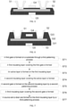
- Embodiments of the present disclosure further provide a method of manufacturing a pixel circuit for manufacturing the fourth transistor T4 and the fifth transistor T5 in any of the pixel circuits described above. Specifically, referring to FIG. 7 , the method includes following steps.
- a first gate is formed on a substrate through a first patterning process.
- the first patterning process mainly includes film forming, coating, exposure, development, etching, and stripping.
- Film forming refers to a process of forming a thin film of a base material on a substrate by magnetron sputtering, evaporation, chemical deposition, etc.
- Coating refers to a process of coating photoresist on the formed thin film of the base material.
- Exposure refers to a process of exposing a specified position of the photoresist using a mask.
- Development refers to a process of removing the photoresist that has undergone a chemical reaction to produce a desired film pattern on a glass.
- Etching refers to a process of etching away a portion of the thin film of the base material that is not covered by the photoresist.
- Stripping refers to a process of removing the photoresist film after the etching.
- the patterning process may also include a substrate cleaning step and a pattern inspection step. In embodiments of the present disclosure, steps included in the patterning process and an order of the steps are not limited, as long as the first gate can be formed.
- a first insulating layer covering the first gate is formed.
- an active layer is formed on the first insulating layer.
- a second insulating layer covering the active layer is formed.
- a second gate is formed on the second insulating layer by a second patterning process.
- a third insulating layer covering the second gate is formed.
- a source and a drain are formed on the third insulating layer by a third patterning process, wherein the source and the drain are in contact with the active layer through through-holes penetrating the second insulating layer and the third insulating layer.
- embodiments of the present disclosure further provide a method of manufacturing a pixel circuit for manufacturing the first transistor T1 to the third transistor T3 and the sixth transistor T6 to the eighth transistor T8 in any of the pixel circuits described above. Specifically, the method includes following steps.
- gates of the first to third transistors T1 ⁇ T3 and gates of the sixth to eighth transistors T6 ⁇ T8 are formed at the same time when the first gate is formed on the substrate by a first patterning process.
- the first insulating layer is formed to also cover the gates of the first to third transistors T3, and the gates of the sixth to eighth transistors T6 ⁇ T8 when the first insulating layer covering the first gate is formed.
- active layers of the first to third transistors T1 ⁇ T3 and active layers of the sixth to eighth transistors T6 ⁇ T8 are formed at the same time when the active layer is formed on the first insulating layer.
- the second insulating layer is formed to also cover the active layers of the first to third transistors T1 ⁇ T3 and the active layers of the sixth to eighth transistors T6 ⁇ T8 when the second insulating layer covering the active layer is formed.
- the second gate is only formed at a position on the second insulating layer corresponding to the first gate.
- the second gate is not formed at positions on the second insulating layer corresponding to the gates of the first to third transistors T1 ⁇ T3, and at positions on the second insulating layer corresponding to the gates of the sixth to eighth transistors T6 ⁇ T8.
- the third insulating layer is formed to only cover the second gate when the third insulating layer covering the second gate is formed.
- the third insulating layer is formed to also cover the second insulating layers of the first to third transistors T1 ⁇ T3, and the second insulating layers of the sixth to eighth transistors T6 ⁇ T8, when the third insulating layer covering the second gate is formed.
- sources and drains of the first to third transistors T1 ⁇ T3, and sources and drains of the sixth to eighth transistors T6 ⁇ T8 are formed at the same time when the source and the drain are formed on the third insulating layer.
- sources and drains of the first to third transistors T1 ⁇ T3, and sources and drains of the sixth to eighth transistors T6 ⁇ T8 may be formed on the second insulating layer covering the active layers of the first to third transistors T1 ⁇ T3, and the active layers of the sixth to eighth transistors T6 ⁇ T8 at the same time when the source and the drain are formed on the third insulating layer.
- Each source and each drain are in contact with a respective active layer through through-holes penetrating the second insulating layer.
- the third insulating layer formed in S85 covers the second insulating layer covering the active layers of the first to third transistors T1 ⁇ T3 and the active layers of the sixth to eighth transistors T6 ⁇ T8, then in S86, sources and drains of the first to third transistors T1 ⁇ T3, and sources and drains of the sixth to eighth transistors T6 ⁇ T8 may be formed on the third insulating layer covering the second insulating layer covering the active layers of the first to third transistors T1 ⁇ T3 and the active layers of the sixth to eighth transistors T6 ⁇ T8 at the same time when the source and the drain are formed on the third insulating layer.
- Each source and each drain are in contact with a respective active layer through through-holes penetrating the second insulating layer and the third insulating layer.
- the first gate may be the gate G4 of the fourth transistor T4, or the gate G5 of the fifth transistor T5.
- the above method of manufacturing a pixel circuit further includes:
- Some embodiments of the present disclosure provide a display panel, which includes any one of the pixel circuits in the embodiments described above.
- the display panel may be an electronic paper, a mobile phone, a tablet computer, a television, a display, a notebook computer, a digital photo frame, a navigator, or any other product or component having a display function.
Landscapes
- Engineering & Computer Science (AREA)
- Physics & Mathematics (AREA)
- Computer Hardware Design (AREA)
- General Physics & Mathematics (AREA)
- Theoretical Computer Science (AREA)
- Control Of Indicators Other Than Cathode Ray Tubes (AREA)
- Control Of El Displays (AREA)
Claims (6)
- Pixelschaltung, umfassend eine Knotensteuerschaltung (11), einen Treiber (12), eine Anzeigeteilschaltung (13), einen Schwellenkompensator (14) und eine Rückstellvorrichtung (15), wobei:die Knotensteuerschaltung (11) konfiguriert ist, ein erstes Abtastsignal (S1), ein zweites Abtastsignal (S2), ein drittes Abtastsignal (S3), eine Referenzspannung (Vref) und eine Datenspannung (Vdata) zu empfangen; die Knotensteuerschaltung (11) weiter konfiguriert ist, die Referenzspannung (Vref) unter Steuerung einer Spannung des ersten Abtastsignals (S1) in einer ersten Dauer und unter Steuerung einer Spannung des zweiten Abtastsignals (S2) in einer vierten Dauer an einen ersten Knoten (N1) auszugeben, und die Datenspannung (Vdata) unter Steuerung einer Spannung des dritten Abtastsignals (S3) in einer dritten Dauer an den ersten Knoten (N1) auszugeben;der Treiber (12) konfiguriert ist, ein erstes Pegelsignal (V1) bei einem Eingangsanschluss (I) des Treibers (12) zu empfangen; ein Steueranschluss (Q) des Treibers (12) direkt mit einem zweiten Knoten (N2) gekoppelt ist; und der Treiber (12) weiter konfiguriert ist, einen Antriebsstrom bei einem Ausgangsanschluss (O) des Treibers (12) unter Steuerung einer Spannung des ersten Pegelsignals (V1) und einer Spannung des zweiten Knotens (N2) in der vierten Dauer auszugeben;die Anzeigeteilschaltung (13) direkt mit der Rückstellvorrichtung (15) und dem Ausgangsanschluss (O) des Treibers (12) gekoppelt ist, die Anzeigeteilschaltung (13) konfiguriert ist, ein zweites Pegelsignal (V2) und das zweite Abtastsignal (S2) zu empfangen, und die Anzeigeteilschaltung (13) weiter konfiguriert ist, eine Grauskala von dem Antriebsstrom unter Steuerung der Spannung des zweiten Abtastsignals (S2) in der vierten Dauer anzuzeigen;der Schwellenkompensator (14) direkt mit dem ersten Knoten (N1), dem Ausgangsanschluss (O) des Treibers (12) und dem zweiten Knoten (N2) gekoppelt ist; der Schwellenkompensator (14) konfiguriert ist, das dritte Abtastsignal (S3) und ein viertes Abtastsignal (S4) zu empfangen; der Schwellenkompensator (14) weiter konfiguriert ist, die Spannung des zweiten Knotens (N2) auf eine Summe der Spannung des ersten Pegelsignals (V1) und einer Schwellenspannung des Treibers (12)unter Steuerung der Spannung des dritten Abtastsignals (S3) in einer zweiten Dauer und unter Steuerung einer Spannung des vierten Abtastsignals (S4) in der dritten Dauer anzupassen, und die Spannung des zweiten Knotens (N2) auf eine Differenz zwischen einer Summe der Spannung des ersten Pegelsignals (V1), der Schwellenspannung des Treibers (12) und der Referenzspannung (Vref) und der Datenspannung (Vdata) unter Steuerung einer Spannung des ersten Knotens (N1) und einer Spannung des Ausgangsanschlusses (O) des Treibers (12) in der vierten Dauer anzupassen;die Rückstellvorrichtung (15) direkt mit dem zweiten Knoten (N2) und der Anzeigeteilschaltung (13) gekoppelt ist; die Rückstellvorrichtung (15) konfiguriert ist, ein Rückstellspannungssignal (Vinit), das erste Abtastsignal (S1) und das dritte Abtastsignal (S3) zu empfangen; die Rückstellvorrichtung (15) weiter konfiguriert ist, den zweiten Knoten (N2) um eine Spannung des Rückstellspannungssignals (Vinit) unter Steuerung der Spannung des ersten Abtastsignals (S1) in der ersten Dauer zurückzustellen, und die Anzeigeteilschaltung (13) um die Spannung des Rückstellspannungssignals (Vinit) unter Steuerung des dritten Abtastsignals (S3) in der zweiten Dauer zurückzustellen;der erste Knoten (N1) ein Schnittpunkt eines Ausgangs der Knotensteuerschaltung (11) und eines Eingangs des Schwellenkompensators (14) ist; undder zweite Knoten (N2) ein Schnittpunkt eines Ausgangs des Schwellenkompensators (14), eines Eingangs des Treibers (12) und eines Ausgangs der Rückstellvorrichtung (15) ist, wobeidie Knotensteuerschaltung (11) einen ersten Transistor (T1), einen zweiten Transistor (T2) und einen dritten Transistor (T3) beinhaltet; der Schwellenkompensator (14) einen vierten Transistor (T4), einen fünften Transistor (T5) und einen ersten Kondensator (C1) umfasst; die Rückstellvorrichtung (15) einen sechsten Transistor (T6) und einen siebten Transistor (T7) umfasst; der Treiber (12) ein Antriebstransistor ist; die Anzeigeteilschaltung (13) einen achten Transistor (T8) und eine lichtemittierende Diode (D1) umfasst;der erste Transistor (T1) konfiguriert ist, die Referenzspannung (Vref) bei einer ersten Elektrode des ersten Transistors (T1) zu empfangen, eine zweite Elektrode des ersten Transistors (T1) direkt mit dem ersten Knoten (N1) gekoppelt ist, und der erste Transistor (T1) konfiguriert ist, das erste Abtastsignal (S1) bei einem Gate des ersten Transistors (T1) zu empfangen;der zweite Transistor (T2) konfiguriert ist, die Referenzspannung (Vref) bei einer ersten Elektrode des zweiten Transistors (T2) zu empfangen, eine zweite Elektrode des zweiten Transistors (T2) direkt mit dem ersten Knoten (N1) gekoppelt ist, und der zweite Transistor (T2) konfiguriert ist, das zweite Abtastsignal (S2) bei einem Gate des zweiten Transistors (T2) zu empfangen;der dritte Transistor (T3) konfiguriert ist, die Datenspannung (Vdata) bei einer ersten Elektrode des dritten Transistors (T3) zu empfangen, eine zweite Elektrode des dritten Transistors (T3) direkt mit dem ersten Knoten (N1) gekoppelt ist, und der dritte Transistor (T3) konfiguriert ist, das dritte Abtastsignal (S3) bei einem Gate des dritten Transistors (T3) zu empfangen;eine erste Elektrode des vierten Transistors (T4) direkt mit dem Ausgangsanschluss (O) des Treibers (12) gekoppelt ist, eine zweite Elektrode des vierten Transistors (T4) direkt mit dem zweiten Knoten (N2) gekoppelt ist, und der vierte Transistor (T4) konfiguriert ist, das dritte Abtastsignal (S3) bei einem Gate (G4) des vierten Transistors (T4) zu empfangen;eine erste Elektrode des fünften Transistors (T5) direkt mit dem Ausgangsanschluss (O) des Treibers (12) gekoppelt ist, eine zweite Elektrode des fünften Transistors (T5) direkt mit dem zweiten Knoten (N2) gekoppelt ist, und der fünfte Transistor (T5) konfiguriert ist, das vierte Abtastsignal (S4) bei einem Gate (G5) des fünften Transistors (T5) zu empfangen;der sechste Transistor (T6) konfiguriert ist, das Rückstellspannungssignal (Vinit) bei einer ersten Elektrode des sechsten Transistors (T6) zu empfangen, eine zweite Elektrode des sechsten Transistors (T6) direkt mit dem zweiten Knoten (N2) gekoppelt ist, und der sechste Transistor (T6) konfiguriert ist, das erste Abtastsignal (S1) bei einem Gate des sechsten Transistors (T6) zu empfangen;der siebte Transistor (T7) konfiguriert ist, das Rückstellspannungssignal (Vinit) bei einer ersten Elektrode des siebten Transistors (T7) zu empfangen, eine zweite Elektrode des siebten Transistors (T7) direkt mit der Anzeigeteilschaltung (13) gekoppelt ist, und der siebte Transistor (T7) konfiguriert ist, das dritte Abtastsignal (S3) bei einem Gate des siebten Transistors (T7) zu empfangen;eine erste Elektrode des ersten Kondensators (C1) direkt mit dem ersten Knoten (N1) gekoppelt ist, und eine zweite Elektrode des ersten Kondensators (C1) direkt mit dem zweiten Knoten (N2) gekoppelt ist;eine erste Elektrode des achten Transistors (T8) direkt mit dem Ausgangsanschluss (O) des Treibers (12) gekoppelt ist, eine zweite Elektrode des achten Transistors (T8) direkt mit einer Anode der lichtemittierenden Diode (D1) gekoppelt ist, und der achte Transistor (T8) konfiguriert ist, das zweite Abtastsignal (S2) bei einem Gate des achten Transistors (T8) zu empfangen;der Eingangsanschluss (I) des Treibers (12) eine Source des Antriebstransistors ist, der Steueranschluss (Q) des Treibers (12) ein Gate des Antriebstransistors ist, und der Ausgangsanschluss (O) des Treibers (12) ein Drain des Antriebstransistors ist;die lichtemittierende Diode (D1) konfiguriert ist, das zweite Pegelsignal (V2) bei einer Kathode der lichtemittierenden Diode (D1) zu empfangen;der vierte Transistor (T4) und der fünfte Transistor (T5) sich eine Source (51), ein Drain (52) und eine aktive Schicht (53) teilen; das Gate (G4) des vierten Transistors (T4) und das Gate (G5) des fünften Transistors (T5) jeweils an beiden Seiten der aktiven Schicht (53) liegen; ein Fortsatz des Gates (G4) des vierten Transistors (T4) in einer Richtung senkrecht zu der aktiven Schicht (53) und ein Fortsatz des Gates (G5) des fünften Transistors (T5) in der Richtung senkrecht zu der aktiven Schicht (53) zusammenfallen; unddas dritte Abtastsignal (S3) ein Ausgangssignal eines Verschiebungsregisters n-ter Stufe in einer Verschiebungsregisterschaltung ist; das vierte Abtastsignal (S4) ein Ausgangssignal eines Verschiebungsregisters (n+1)-ter Stufe in der Verschiebungsregisterschaltung ist, und n eine positive Ganzzahl ist.
- Pixelschaltung nach Anspruch 1, wobei eine erste Isolierschicht (GI1) weiter zwischen dem Gate (G5) des fünften Transistors (T5) und der aktiven Schicht (53) angeordnet ist; eine zweite Isolierschicht (GI2) weiter zwischen dem Gate (G4) des vierten Transistors (T4) und der aktiven Schicht (53) angeordnet ist; eine dritte Isolierschicht (GI3) weiter zwischen dem Gate (G4) des vierten Transistors (T4) und sowohl der Source (51) als auch dem Drain (52) angeordnet ist; und die Source (51) und der Drain (52) in Kontakt mit der aktiven Schicht (53) durch Durchgangslöcher sind, die die zweite Isolierschicht (GI2) und die dritte Isolierschicht (GI3) durchdringen.
- Pixelschaltung nach Anspruch 1, wobei die erste Elektrode des ersten Kondensators (C1) und das Gate (G4) des vierten Transistors (T4) durch einen selben Strukturierungsprozess gebildet werden, und die zweite Elektrode des ersten Kondensators (C1) und das Gate (G5) des fünften Transistors (T5) durch einen selben Strukturierungsprozess gebildet werden.
- Pixelschaltung nach Anspruch 1, wobei die erste Elektrode des ersten Kondensators (C1) und das Gate (G5) des fünften Transistors (T5) durch einen selben Strukturierungsprozess gebildet werden, und die zweite Elektrode des ersten Kondensators (C1) und das Gate (G4) des vierten Transistors (T4) durch einen selben Strukturierungsprozess gebildet werden.
- Verfahren zum Antreiben der Pixelschaltung nach einem der Ansprüche 1 bis 4, dadurch gekennzeichnet, dass:
das Verfahren umfasst:in einer ersten Dauer, Ausgeben, durch die Knotensteuerschaltung (11), der Referenzspannung (Vref) an den ersten Knoten (N1) unter der Steuerung der Spannung des ersten Abtastsignals (S1); und Zurückstellen, durch die Rückstellvorrichtung (15), des zweiten Knotens (N2) um die Spannung des Rückstellspannungssignals (Vinit) unter der Steuerung der Spannung des ersten Abtastsignals (S1);in einer zweiten Dauer, Ausgeben, durch die Knotensteuerschaltung (11), der Datenspannung (Vdata) an den ersten Knoten (N1) unter der Steuerung der Spannung des dritten Abtastsignals (S3); Anpassen, durch den Schwellenkompensator (14), der Spannung des zweiten Knotens (N2) an die Summe der Spannung des ersten Pegelsignals (V1) und der Schwellenspannung des Treibers (12); und Zurückstellen, durch eine Rückstellvorrichtung (15), der Anzeigeteilschaltung (13) um die Spannung des Rückstellspannungssignals (Vinit) unter der Steuerung der Spannung des dritten Abtastsignals (S3);in einer dritten Dauer, Anpassen, durch den Schwellenkompensator (14), der Spannung des zweiten Knotens (N2) auf die Summe der Spannung des ersten Pegelsignals (V1) und der Schwellenspannung des Treibers (12) unter der Steuerung der Spannung des vierten Abtastsignals (S4); undin einer vierten Dauer, Ausgeben, durch die Knotensteuerschaltung (11), der Referenzspannung (Vref) an den ersten Knoten (N1) unter der Steuerung der Spannung des zweiten Abtastsignals (S2); Anpassen, durch den Schwellenkompensator (14), der Spannung des zweiten Knotens (N2) an die Differenz zwischen der Summe der Spannung des ersten Pegelsignals (V1), der Schwellenspannung des Treibers (12) und der Referenzspannung (Vref), und der Datenspannung (Vdata) unter der Steuerung der Spannung des ersten Knotens (N1) und der Spannung des Ausgangsanschlusses (O) des Treibers (12); Ausgeben, durch den Treiber (12) des Antriebsstroms am Ausgangsanschluss (O) des Treibers 12, unter der Steuerung der Spannung des ersten Pegelsignals (V1) und der Spannung des zweiten Knotens (N2); und Antreiben, durch die Anzeigeteilschaltung (13), eine Grauskala von dem Antriebsstrom unter der Steuerung der Spannung des zweiten Abtastsignals (S2) anzuzeigen, wobeiin der ersten Dauer, der erste Transistor (T1) und der sechste Transistor (T6) unter der Steuerung der Spannung des ersten Abtastsignals (S1) eingeschaltet werden, und die Referenzspannung (Vref) an den ersten Knoten (N1) durch den ersten Transistor (T1) übertragen wird, und das Rückstellspannungssignal (Vinit) an den zweiten Knoten (N2) durch den sechsten Transistor (T6) übertragen wird; die erste und die zweite Elektrode des ersten Kondensators C1 die Referenzspannung (Vref) beziehungsweise das Rückstellspannungssignal (Vinit) speichern;in der zweiten Dauer, der dritte Transistor (T3), der vierte Transistor (T4) und der siebte Transistor (T7) unter der Steuerung der Spannung des dritten Abtastsignals (S3) eingeschaltet werden, und das Gate des Antriebstransistors mit dem Drain des Antriebstransistors gekoppelt ist, und die Datenspannung (Vdata) an den ersten Knoten (N1) durch den dritten Transistor (T3) übertragen wird, die Spannung des zweiten Knotens (N2) an die Summe der Spannung des ersten Pegelsignals (V1) und der Schwellenspannung des Antriebstransistors angepasst wird, und die erste und die zweite Elektrode des ersten Kondensators C1 die Datenspannung (Vdata) beziehungsweise die Spannung des zweiten Knotens (N2) speichern, und eine Anodenspannung der lichtemittierenden Diode (D1) auf die Spannung des Rückstellspannungssignals (Vinit) durch den siebten Transistor (T7) zurückgestellt wird;in der dritten Dauer, der fünfte Transistor (T5) unter der Steuerung der Spannung des vierten Abtastsignals (S4) eingeschaltet wird, und das Gate des Antriebstransistors mit dem Drain des Antriebstransistors gekoppelt gehalten wird, und die Spannung des zweiten Knotens (N2) weiter an die Summe der Spannung des ersten Pegelsignals (V1) und der Schwellenspannung des Antriebstransistors angepasst wird; die zweite Elektrode des ersten Kondensators C1 die Spannung des zweiten Knotens (N2) speichert;in der vierten Dauer, der zweite Transistor (T2) und der achte Transistor (T8) unter der Steuerung der Spannung des zweiten Abtastsignals (S2) eingeschaltet werden, und die Referenzspannung (Vref) an den ersten Knoten (N1) durch den zweiten Transistor (T2) übertragen wird, und die Spannung des zweiten Knotens (N2) an die Differenz zwischen der Summe der Spannung des ersten Pegelsignals (V1), der Schwellenspannung des Antriebstransistors und der Referenzspannung (Vref), und der Datenspannung (Vdata) unter der Steuerung der Spannung des ersten Knotens (N1) und der Spannung des Ausgangsanschlusses (O) des Treibers (12) angepasst wird, und der Antriebsstrom bei dem Drain des Antriebstransistors in die lichtemittierende Diode (D1) durch den achten Transistor (T8) unter der Steuerung der Spannung des ersten Pegelsignals (V1) und der Spannung des zweiten Knotens (N2) ausgegeben wird; und die lichtemittierende Diode (D1) angetrieben wird, die Grauskala anzuzeigen. - Anzeigepaneel, umfassend Pixelschaltungen nach einem der Ansprüche 1 bis 4.
Applications Claiming Priority (2)
| Application Number | Priority Date | Filing Date | Title |
|---|---|---|---|
| CN201710428659.0A CN107204173B (zh) | 2017-06-08 | 2017-06-08 | 一种像素电路及其驱动方法、显示面板 |
| PCT/CN2018/082632 WO2018223767A1 (zh) | 2017-06-08 | 2018-04-11 | 像素电路及其驱动方法、显示面板 |
Publications (3)
| Publication Number | Publication Date |
|---|---|
| EP3637405A1 EP3637405A1 (de) | 2020-04-15 |
| EP3637405A4 EP3637405A4 (de) | 2021-03-03 |
| EP3637405B1 true EP3637405B1 (de) | 2022-03-23 |
Family
ID=59907342
Family Applications (1)
| Application Number | Title | Priority Date | Filing Date |
|---|---|---|---|
| EP18814246.7A Active EP3637405B1 (de) | 2017-06-08 | 2018-04-11 | Pixelschaltung und ansteuerungsverfahren dafür sowie anzeigetafel |
Country Status (4)
| Country | Link |
|---|---|
| US (1) | US10937367B2 (de) |
| EP (1) | EP3637405B1 (de) |
| CN (1) | CN107204173B (de) |
| WO (1) | WO2018223767A1 (de) |
Families Citing this family (12)
| Publication number | Priority date | Publication date | Assignee | Title |
|---|---|---|---|---|
| CN107204173B (zh) | 2017-06-08 | 2019-06-28 | 京东方科技集团股份有限公司 | 一种像素电路及其驱动方法、显示面板 |
| CN108231005A (zh) * | 2018-03-29 | 2018-06-29 | 武汉华星光电半导体显示技术有限公司 | Amoled像素驱动电路、驱动方法、显示面板及终端 |
| CN109686314B (zh) | 2019-03-01 | 2021-01-29 | 京东方科技集团股份有限公司 | 像素电路、显示基板和显示装置 |
| TWI703547B (zh) * | 2019-06-13 | 2020-09-01 | 友達光電股份有限公司 | 畫素補償電路 |
| CN110675822A (zh) * | 2019-09-30 | 2020-01-10 | 昆山国显光电有限公司 | 像素驱动电路及像素驱动电路的控制方法 |
| CN111477178A (zh) * | 2020-05-26 | 2020-07-31 | 京东方科技集团股份有限公司 | 一种像素驱动电路及其驱动方法、显示装置 |
| CN111627387B (zh) | 2020-06-24 | 2022-09-02 | 京东方科技集团股份有限公司 | 像素驱动电路及其驱动方法、显示面板及显示装置 |
| CN114420037A (zh) * | 2020-10-12 | 2022-04-29 | 群创光电股份有限公司 | 用于驱动光发射单元的驱动电路以及电子装置 |
| CN113223458B (zh) * | 2021-01-25 | 2023-01-31 | 重庆京东方显示技术有限公司 | 一种像素电路及其驱动方法、显示基板和显示装置 |
| WO2023050196A1 (zh) * | 2021-09-29 | 2023-04-06 | 京东方科技集团股份有限公司 | 像素驱动电路及像素驱动方法、显示面板 |
| CN116759426A (zh) * | 2022-03-04 | 2023-09-15 | 敦泰电子股份有限公司 | 薄膜晶体管感光电路、显示面板、使用其的行动装置以及其制造方法 |
| TWI845230B (zh) * | 2023-03-27 | 2024-06-11 | 友達光電股份有限公司 | 畫素電路及應用其之顯示面板 |
Family Cites Families (18)
| Publication number | Priority date | Publication date | Assignee | Title |
|---|---|---|---|---|
| KR101097325B1 (ko) * | 2009-12-31 | 2011-12-23 | 삼성모바일디스플레이주식회사 | 화소 회로 및 유기 전계 발광 표시 장치 |
| KR101125571B1 (ko) | 2010-02-05 | 2012-03-22 | 삼성모바일디스플레이주식회사 | 화소, 이를 이용한 표시 장치 및 그 구동 방법 |
| KR101152575B1 (ko) * | 2010-05-10 | 2012-06-01 | 삼성모바일디스플레이주식회사 | 평판 표시 장치의 화소 회로 및 그의 구동 방법 |
| KR20150006145A (ko) | 2013-07-08 | 2015-01-16 | 삼성디스플레이 주식회사 | 화소 및 이를 이용한 유기전계발광 표시장치 |
| CN103531148B (zh) | 2013-10-31 | 2015-07-08 | 京东方科技集团股份有限公司 | 一种交流驱动的像素电路、驱动方法及显示装置 |
| CN105225636B (zh) * | 2014-06-13 | 2017-05-31 | 京东方科技集团股份有限公司 | 像素驱动电路、驱动方法、阵列基板及显示装置 |
| CN203882587U (zh) * | 2014-06-13 | 2014-10-15 | 京东方科技集团股份有限公司 | 像素驱动电路、阵列基板及显示装置 |
| KR102334265B1 (ko) | 2014-12-02 | 2021-12-01 | 삼성디스플레이 주식회사 | 유기 발광 표시 장치 및 이의 구동 방법 |
| CN204315211U (zh) * | 2014-12-18 | 2015-05-06 | 合肥鑫晟光电科技有限公司 | 像素驱动电路和显示装置 |
| CN104575378B (zh) | 2014-12-23 | 2017-07-28 | 北京大学深圳研究生院 | 像素电路、显示装置及显示驱动方法 |
| CN104599638A (zh) * | 2015-02-12 | 2015-05-06 | 京东方科技集团股份有限公司 | 一种像素电路及其驱动方法和显示装置 |
| KR102307500B1 (ko) * | 2015-03-20 | 2021-10-01 | 삼성디스플레이 주식회사 | 표시 장치의 화소회로 및 이를 포함하는 표시 장치 |
| CN105185305A (zh) * | 2015-09-10 | 2015-12-23 | 京东方科技集团股份有限公司 | 一种像素电路、其驱动方法及相关装置 |
| CN105489163A (zh) * | 2016-01-04 | 2016-04-13 | 京东方科技集团股份有限公司 | 一种像素电路及其驱动方法和显示装置 |
| CN106097964B (zh) * | 2016-08-22 | 2018-09-18 | 京东方科技集团股份有限公司 | 像素电路、显示面板、显示设备及驱动方法 |
| CN205920745U (zh) * | 2016-08-22 | 2017-02-01 | 京东方科技集团股份有限公司 | 像素电路、显示面板及显示设备 |
| CN106504700B (zh) | 2016-10-14 | 2018-03-06 | 深圳市华星光电技术有限公司 | Amoled像素驱动电路及驱动方法 |
| CN107204173B (zh) * | 2017-06-08 | 2019-06-28 | 京东方科技集团股份有限公司 | 一种像素电路及其驱动方法、显示面板 |
-
2017
- 2017-06-08 CN CN201710428659.0A patent/CN107204173B/zh active Active
-
2018
- 2018-04-11 US US16/330,639 patent/US10937367B2/en active Active
- 2018-04-11 EP EP18814246.7A patent/EP3637405B1/de active Active
- 2018-04-11 WO PCT/CN2018/082632 patent/WO2018223767A1/zh not_active Ceased
Also Published As
| Publication number | Publication date |
|---|---|
| US20210005143A1 (en) | 2021-01-07 |
| EP3637405A1 (de) | 2020-04-15 |
| CN107204173B (zh) | 2019-06-28 |
| CN107204173A (zh) | 2017-09-26 |
| US10937367B2 (en) | 2021-03-02 |
| EP3637405A4 (de) | 2021-03-03 |
| WO2018223767A1 (zh) | 2018-12-13 |
Similar Documents
| Publication | Publication Date | Title |
|---|---|---|
| EP3637405B1 (de) | Pixelschaltung und ansteuerungsverfahren dafür sowie anzeigetafel | |
| US11569311B2 (en) | Array substrate with sub-pixels including power-supplying wire portions having openings therebetween and manufacturing method thereof, and display panel | |
| US11062645B1 (en) | Display device | |
| US11683957B2 (en) | Display panel and display device | |
| US9564081B2 (en) | Pixel compensation circuit, array substrate and display apparatus | |
| US11263960B2 (en) | Display panel, driving method and display device | |
| US10657889B2 (en) | Pixel circuit, driving method thereof and display device | |
| US10679555B2 (en) | Pixel circuit and method for driving the same, and display apparatus | |
| US9595223B2 (en) | Pixel driving circuit and driving method thereof, array substrate and display apparatus | |
| US10770000B2 (en) | Pixel circuit, driving method, display panel and display device | |
| CN112670305B (zh) | 显示面板和显示装置 | |
| US20130335307A1 (en) | Displays with pixel circuits capable of compensating for transistor threshold voltage drift | |
| US11217160B2 (en) | Pixel circuit and method of driving the same, and display device | |
| CN105185306A (zh) | 像素电路及其驱动方法、显示基板及显示装置 | |
| CN105161051A (zh) | 像素电路及其驱动方法、阵列基板、显示面板及显示装置 | |
| US20190164488A1 (en) | Pixel circuit and driving method thereof, and display device | |
| US10978535B2 (en) | Pixel circuit, display panel and display device | |
| US12437692B2 (en) | Display panel, integrated chip component and display device | |
| US20220076622A1 (en) | Pixel driving circuit and driving method therefor, display panel and display apparatus | |
| CN111724743A (zh) | 像素驱动电路及其驱动方法、显示装置 | |
| US12364016B2 (en) | Display substrate including a shift register at an edge area of a base substrate, and display device | |
| US9805655B2 (en) | Pixel circuit and driving method thereof, display device | |
| CN115835730A (zh) | 显示基板以及显示装置 | |
| US12563923B2 (en) | Display substrate that includes an initialization signal film layer with a plurality of portions and sub-portions, method of manufacturing the same and display device |
Legal Events
| Date | Code | Title | Description |
|---|---|---|---|
| STAA | Information on the status of an ep patent application or granted ep patent |
Free format text: STATUS: THE INTERNATIONAL PUBLICATION HAS BEEN MADE |
|
| PUAI | Public reference made under article 153(3) epc to a published international application that has entered the european phase |
Free format text: ORIGINAL CODE: 0009012 |
|
| STAA | Information on the status of an ep patent application or granted ep patent |
Free format text: STATUS: REQUEST FOR EXAMINATION WAS MADE |
|
| 17P | Request for examination filed |
Effective date: 20190306 |
|
| AK | Designated contracting states |
Kind code of ref document: A1 Designated state(s): AL AT BE BG CH CY CZ DE DK EE ES FI FR GB GR HR HU IE IS IT LI LT LU LV MC MK MT NL NO PL PT RO RS SE SI SK SM TR |
|
| AX | Request for extension of the european patent |
Extension state: BA ME |
|
| DAV | Request for validation of the european patent (deleted) | ||
| DAX | Request for extension of the european patent (deleted) | ||
| A4 | Supplementary search report drawn up and despatched |
Effective date: 20210201 |
|
| RIC1 | Information provided on ipc code assigned before grant |
Ipc: G09G 3/3233 20160101ALI20210126BHEP Ipc: G09G 3/3258 20160101AFI20210126BHEP |
|
| GRAP | Despatch of communication of intention to grant a patent |
Free format text: ORIGINAL CODE: EPIDOSNIGR1 |
|
| STAA | Information on the status of an ep patent application or granted ep patent |
Free format text: STATUS: GRANT OF PATENT IS INTENDED |
|
| INTG | Intention to grant announced |
Effective date: 20211103 |
|
| GRAS | Grant fee paid |
Free format text: ORIGINAL CODE: EPIDOSNIGR3 |
|
| GRAA | (expected) grant |
Free format text: ORIGINAL CODE: 0009210 |
|
| STAA | Information on the status of an ep patent application or granted ep patent |
Free format text: STATUS: THE PATENT HAS BEEN GRANTED |
|
| AK | Designated contracting states |
Kind code of ref document: B1 Designated state(s): AL AT BE BG CH CY CZ DE DK EE ES FI FR GB GR HR HU IE IS IT LI LT LU LV MC MK MT NL NO PL PT RO RS SE SI SK SM TR |
|
| REG | Reference to a national code |
Ref country code: GB Ref legal event code: FG4D |
|
| REG | Reference to a national code |
Ref country code: CH Ref legal event code: EP |
|
| REG | Reference to a national code |
Ref country code: IE Ref legal event code: FG4D |
|
| REG | Reference to a national code |
Ref country code: DE Ref legal event code: R096 Ref document number: 602018032718 Country of ref document: DE |
|
| REG | Reference to a national code |
Ref country code: AT Ref legal event code: REF Ref document number: 1477997 Country of ref document: AT Kind code of ref document: T Effective date: 20220415 |
|
| REG | Reference to a national code |
Ref country code: LT Ref legal event code: MG9D |
|
| REG | Reference to a national code |
Ref country code: NL Ref legal event code: MP Effective date: 20220323 |
|
| PG25 | Lapsed in a contracting state [announced via postgrant information from national office to epo] |
Ref country code: SE Free format text: LAPSE BECAUSE OF FAILURE TO SUBMIT A TRANSLATION OF THE DESCRIPTION OR TO PAY THE FEE WITHIN THE PRESCRIBED TIME-LIMIT Effective date: 20220323 Ref country code: RS Free format text: LAPSE BECAUSE OF FAILURE TO SUBMIT A TRANSLATION OF THE DESCRIPTION OR TO PAY THE FEE WITHIN THE PRESCRIBED TIME-LIMIT Effective date: 20220323 Ref country code: NO Free format text: LAPSE BECAUSE OF FAILURE TO SUBMIT A TRANSLATION OF THE DESCRIPTION OR TO PAY THE FEE WITHIN THE PRESCRIBED TIME-LIMIT Effective date: 20220623 Ref country code: LT Free format text: LAPSE BECAUSE OF FAILURE TO SUBMIT A TRANSLATION OF THE DESCRIPTION OR TO PAY THE FEE WITHIN THE PRESCRIBED TIME-LIMIT Effective date: 20220323 Ref country code: HR Free format text: LAPSE BECAUSE OF FAILURE TO SUBMIT A TRANSLATION OF THE DESCRIPTION OR TO PAY THE FEE WITHIN THE PRESCRIBED TIME-LIMIT Effective date: 20220323 Ref country code: BG Free format text: LAPSE BECAUSE OF FAILURE TO SUBMIT A TRANSLATION OF THE DESCRIPTION OR TO PAY THE FEE WITHIN THE PRESCRIBED TIME-LIMIT Effective date: 20220623 |
|
| REG | Reference to a national code |
Ref country code: AT Ref legal event code: MK05 Ref document number: 1477997 Country of ref document: AT Kind code of ref document: T Effective date: 20220323 |
|
| PG25 | Lapsed in a contracting state [announced via postgrant information from national office to epo] |
Ref country code: LV Free format text: LAPSE BECAUSE OF FAILURE TO SUBMIT A TRANSLATION OF THE DESCRIPTION OR TO PAY THE FEE WITHIN THE PRESCRIBED TIME-LIMIT Effective date: 20220323 Ref country code: GR Free format text: LAPSE BECAUSE OF FAILURE TO SUBMIT A TRANSLATION OF THE DESCRIPTION OR TO PAY THE FEE WITHIN THE PRESCRIBED TIME-LIMIT Effective date: 20220624 Ref country code: FI Free format text: LAPSE BECAUSE OF FAILURE TO SUBMIT A TRANSLATION OF THE DESCRIPTION OR TO PAY THE FEE WITHIN THE PRESCRIBED TIME-LIMIT Effective date: 20220323 |
|
| PG25 | Lapsed in a contracting state [announced via postgrant information from national office to epo] |
Ref country code: NL Free format text: LAPSE BECAUSE OF FAILURE TO SUBMIT A TRANSLATION OF THE DESCRIPTION OR TO PAY THE FEE WITHIN THE PRESCRIBED TIME-LIMIT Effective date: 20220323 |
|
| PG25 | Lapsed in a contracting state [announced via postgrant information from national office to epo] |
Ref country code: SM Free format text: LAPSE BECAUSE OF FAILURE TO SUBMIT A TRANSLATION OF THE DESCRIPTION OR TO PAY THE FEE WITHIN THE PRESCRIBED TIME-LIMIT Effective date: 20220323 Ref country code: SK Free format text: LAPSE BECAUSE OF FAILURE TO SUBMIT A TRANSLATION OF THE DESCRIPTION OR TO PAY THE FEE WITHIN THE PRESCRIBED TIME-LIMIT Effective date: 20220323 Ref country code: RO Free format text: LAPSE BECAUSE OF FAILURE TO SUBMIT A TRANSLATION OF THE DESCRIPTION OR TO PAY THE FEE WITHIN THE PRESCRIBED TIME-LIMIT Effective date: 20220323 Ref country code: PT Free format text: LAPSE BECAUSE OF FAILURE TO SUBMIT A TRANSLATION OF THE DESCRIPTION OR TO PAY THE FEE WITHIN THE PRESCRIBED TIME-LIMIT Effective date: 20220725 Ref country code: ES Free format text: LAPSE BECAUSE OF FAILURE TO SUBMIT A TRANSLATION OF THE DESCRIPTION OR TO PAY THE FEE WITHIN THE PRESCRIBED TIME-LIMIT Effective date: 20220323 Ref country code: EE Free format text: LAPSE BECAUSE OF FAILURE TO SUBMIT A TRANSLATION OF THE DESCRIPTION OR TO PAY THE FEE WITHIN THE PRESCRIBED TIME-LIMIT Effective date: 20220323 Ref country code: CZ Free format text: LAPSE BECAUSE OF FAILURE TO SUBMIT A TRANSLATION OF THE DESCRIPTION OR TO PAY THE FEE WITHIN THE PRESCRIBED TIME-LIMIT Effective date: 20220323 Ref country code: AT Free format text: LAPSE BECAUSE OF FAILURE TO SUBMIT A TRANSLATION OF THE DESCRIPTION OR TO PAY THE FEE WITHIN THE PRESCRIBED TIME-LIMIT Effective date: 20220323 |
|
| PG25 | Lapsed in a contracting state [announced via postgrant information from national office to epo] |
Ref country code: PL Free format text: LAPSE BECAUSE OF FAILURE TO SUBMIT A TRANSLATION OF THE DESCRIPTION OR TO PAY THE FEE WITHIN THE PRESCRIBED TIME-LIMIT Effective date: 20220323 Ref country code: IS Free format text: LAPSE BECAUSE OF FAILURE TO SUBMIT A TRANSLATION OF THE DESCRIPTION OR TO PAY THE FEE WITHIN THE PRESCRIBED TIME-LIMIT Effective date: 20220723 Ref country code: AL Free format text: LAPSE BECAUSE OF FAILURE TO SUBMIT A TRANSLATION OF THE DESCRIPTION OR TO PAY THE FEE WITHIN THE PRESCRIBED TIME-LIMIT Effective date: 20220323 |
|
| REG | Reference to a national code |
Ref country code: CH Ref legal event code: PL |
|
| REG | Reference to a national code |
Ref country code: DE Ref legal event code: R097 Ref document number: 602018032718 Country of ref document: DE |
|
| REG | Reference to a national code |
Ref country code: BE Ref legal event code: MM Effective date: 20220430 |
|
| PLBE | No opposition filed within time limit |
Free format text: ORIGINAL CODE: 0009261 |
|
| STAA | Information on the status of an ep patent application or granted ep patent |
Free format text: STATUS: NO OPPOSITION FILED WITHIN TIME LIMIT |
|
| PG25 | Lapsed in a contracting state [announced via postgrant information from national office to epo] |
Ref country code: MC Free format text: LAPSE BECAUSE OF FAILURE TO SUBMIT A TRANSLATION OF THE DESCRIPTION OR TO PAY THE FEE WITHIN THE PRESCRIBED TIME-LIMIT Effective date: 20220323 Ref country code: LU Free format text: LAPSE BECAUSE OF NON-PAYMENT OF DUE FEES Effective date: 20220411 Ref country code: LI Free format text: LAPSE BECAUSE OF NON-PAYMENT OF DUE FEES Effective date: 20220430 Ref country code: DK Free format text: LAPSE BECAUSE OF FAILURE TO SUBMIT A TRANSLATION OF THE DESCRIPTION OR TO PAY THE FEE WITHIN THE PRESCRIBED TIME-LIMIT Effective date: 20220323 Ref country code: CH Free format text: LAPSE BECAUSE OF NON-PAYMENT OF DUE FEES Effective date: 20220430 |
|
| PG25 | Lapsed in a contracting state [announced via postgrant information from national office to epo] |
Ref country code: BE Free format text: LAPSE BECAUSE OF NON-PAYMENT OF DUE FEES Effective date: 20220430 |
|
| 26N | No opposition filed |
Effective date: 20230102 |
|
| GBPC | Gb: european patent ceased through non-payment of renewal fee |
Effective date: 20220623 |
|
| PG25 | Lapsed in a contracting state [announced via postgrant information from national office to epo] |
Ref country code: IE Free format text: LAPSE BECAUSE OF NON-PAYMENT OF DUE FEES Effective date: 20220411 Ref country code: FR Free format text: LAPSE BECAUSE OF NON-PAYMENT OF DUE FEES Effective date: 20220523 |
|
| PG25 | Lapsed in a contracting state [announced via postgrant information from national office to epo] |
Ref country code: SI Free format text: LAPSE BECAUSE OF FAILURE TO SUBMIT A TRANSLATION OF THE DESCRIPTION OR TO PAY THE FEE WITHIN THE PRESCRIBED TIME-LIMIT Effective date: 20220323 Ref country code: GB Free format text: LAPSE BECAUSE OF NON-PAYMENT OF DUE FEES Effective date: 20220623 |
|
| PG25 | Lapsed in a contracting state [announced via postgrant information from national office to epo] |
Ref country code: IT Free format text: LAPSE BECAUSE OF FAILURE TO SUBMIT A TRANSLATION OF THE DESCRIPTION OR TO PAY THE FEE WITHIN THE PRESCRIBED TIME-LIMIT Effective date: 20220323 |
|
| PG25 | Lapsed in a contracting state [announced via postgrant information from national office to epo] |
Ref country code: MK Free format text: LAPSE BECAUSE OF FAILURE TO SUBMIT A TRANSLATION OF THE DESCRIPTION OR TO PAY THE FEE WITHIN THE PRESCRIBED TIME-LIMIT Effective date: 20220323 Ref country code: CY Free format text: LAPSE BECAUSE OF FAILURE TO SUBMIT A TRANSLATION OF THE DESCRIPTION OR TO PAY THE FEE WITHIN THE PRESCRIBED TIME-LIMIT Effective date: 20220323 |
|
| PG25 | Lapsed in a contracting state [announced via postgrant information from national office to epo] |
Ref country code: HU Free format text: LAPSE BECAUSE OF FAILURE TO SUBMIT A TRANSLATION OF THE DESCRIPTION OR TO PAY THE FEE WITHIN THE PRESCRIBED TIME-LIMIT; INVALID AB INITIO Effective date: 20180411 |
|
| PG25 | Lapsed in a contracting state [announced via postgrant information from national office to epo] |
Ref country code: MT Free format text: LAPSE BECAUSE OF FAILURE TO SUBMIT A TRANSLATION OF THE DESCRIPTION OR TO PAY THE FEE WITHIN THE PRESCRIBED TIME-LIMIT Effective date: 20220323 |
|
| PGFP | Annual fee paid to national office [announced via postgrant information from national office to epo] |
Ref country code: DE Payment date: 20250422 Year of fee payment: 8 |
|
| PG25 | Lapsed in a contracting state [announced via postgrant information from national office to epo] |
Ref country code: TR Free format text: LAPSE BECAUSE OF FAILURE TO SUBMIT A TRANSLATION OF THE DESCRIPTION OR TO PAY THE FEE WITHIN THE PRESCRIBED TIME-LIMIT Effective date: 20220323 |