EP3637450A2 - Matériau d'électrode négative pour pseudocondensateur et son procédé de fabrication - Google Patents
Matériau d'électrode négative pour pseudocondensateur et son procédé de fabrication Download PDFInfo
- Publication number
- EP3637450A2 EP3637450A2 EP18858129.2A EP18858129A EP3637450A2 EP 3637450 A2 EP3637450 A2 EP 3637450A2 EP 18858129 A EP18858129 A EP 18858129A EP 3637450 A2 EP3637450 A2 EP 3637450A2
- Authority
- EP
- European Patent Office
- Prior art keywords
- pseudocapacitor
- metal oxide
- conductive inorganic
- anode
- anode material
- Prior art date
- Legal status (The legal status is an assumption and is not a legal conclusion. Google has not performed a legal analysis and makes no representation as to the accuracy of the status listed.)
- Granted
Links
Images





Classifications
-
- H—ELECTRICITY
- H01—ELECTRIC ELEMENTS
- H01G—CAPACITORS; CAPACITORS, RECTIFIERS, DETECTORS, SWITCHING DEVICES, LIGHT-SENSITIVE OR TEMPERATURE-SENSITIVE DEVICES OF THE ELECTROLYTIC TYPE
- H01G11/00—Hybrid capacitors, i.e. capacitors having different positive and negative electrodes; Electric double-layer [EDL] capacitors; Processes for the manufacture thereof or of parts thereof
- H01G11/02—Hybrid capacitors, i.e. capacitors having different positive and negative electrodes; Electric double-layer [EDL] capacitors; Processes for the manufacture thereof or of parts thereof using combined reduction-oxidation reactions, e.g. redox arrangement or solion
-
- B—PERFORMING OPERATIONS; TRANSPORTING
- B82—NANOTECHNOLOGY
- B82Y—SPECIFIC USES OR APPLICATIONS OF NANOSTRUCTURES; MEASUREMENT OR ANALYSIS OF NANOSTRUCTURES; MANUFACTURE OR TREATMENT OF NANOSTRUCTURES
- B82Y30/00—Nanotechnology for materials or surface science, e.g. nanocomposites
-
- H—ELECTRICITY
- H01—ELECTRIC ELEMENTS
- H01G—CAPACITORS; CAPACITORS, RECTIFIERS, DETECTORS, SWITCHING DEVICES, LIGHT-SENSITIVE OR TEMPERATURE-SENSITIVE DEVICES OF THE ELECTROLYTIC TYPE
- H01G11/00—Hybrid capacitors, i.e. capacitors having different positive and negative electrodes; Electric double-layer [EDL] capacitors; Processes for the manufacture thereof or of parts thereof
- H01G11/22—Electrodes
- H01G11/24—Electrodes characterised by structural features of the materials making up or comprised in the electrodes, e.g. form, surface area or porosity; characterised by the structural features of powders or particles used therefor
-
- H—ELECTRICITY
- H01—ELECTRIC ELEMENTS
- H01G—CAPACITORS; CAPACITORS, RECTIFIERS, DETECTORS, SWITCHING DEVICES, LIGHT-SENSITIVE OR TEMPERATURE-SENSITIVE DEVICES OF THE ELECTROLYTIC TYPE
- H01G11/00—Hybrid capacitors, i.e. capacitors having different positive and negative electrodes; Electric double-layer [EDL] capacitors; Processes for the manufacture thereof or of parts thereof
- H01G11/22—Electrodes
- H01G11/30—Electrodes characterised by their material
- H01G11/32—Carbon-based
- H01G11/36—Nanostructures, e.g. nanofibres, nanotubes or fullerenes
-
- H—ELECTRICITY
- H01—ELECTRIC ELEMENTS
- H01G—CAPACITORS; CAPACITORS, RECTIFIERS, DETECTORS, SWITCHING DEVICES, LIGHT-SENSITIVE OR TEMPERATURE-SENSITIVE DEVICES OF THE ELECTROLYTIC TYPE
- H01G11/00—Hybrid capacitors, i.e. capacitors having different positive and negative electrodes; Electric double-layer [EDL] capacitors; Processes for the manufacture thereof or of parts thereof
- H01G11/22—Electrodes
- H01G11/30—Electrodes characterised by their material
- H01G11/46—Metal oxides
-
- H—ELECTRICITY
- H01—ELECTRIC ELEMENTS
- H01G—CAPACITORS; CAPACITORS, RECTIFIERS, DETECTORS, SWITCHING DEVICES, LIGHT-SENSITIVE OR TEMPERATURE-SENSITIVE DEVICES OF THE ELECTROLYTIC TYPE
- H01G11/00—Hybrid capacitors, i.e. capacitors having different positive and negative electrodes; Electric double-layer [EDL] capacitors; Processes for the manufacture thereof or of parts thereof
- H01G11/22—Electrodes
- H01G11/30—Electrodes characterised by their material
- H01G11/50—Electrodes characterised by their material specially adapted for lithium-ion capacitors, e.g. for lithium-doping or for intercalation
-
- H—ELECTRICITY
- H01—ELECTRIC ELEMENTS
- H01G—CAPACITORS; CAPACITORS, RECTIFIERS, DETECTORS, SWITCHING DEVICES, LIGHT-SENSITIVE OR TEMPERATURE-SENSITIVE DEVICES OF THE ELECTROLYTIC TYPE
- H01G11/00—Hybrid capacitors, i.e. capacitors having different positive and negative electrodes; Electric double-layer [EDL] capacitors; Processes for the manufacture thereof or of parts thereof
- H01G11/84—Processes for the manufacture of hybrid or EDL capacitors, or components thereof
- H01G11/86—Processes for the manufacture of hybrid or EDL capacitors, or components thereof specially adapted for electrodes
-
- Y—GENERAL TAGGING OF NEW TECHNOLOGICAL DEVELOPMENTS; GENERAL TAGGING OF CROSS-SECTIONAL TECHNOLOGIES SPANNING OVER SEVERAL SECTIONS OF THE IPC; TECHNICAL SUBJECTS COVERED BY FORMER USPC CROSS-REFERENCE ART COLLECTIONS [XRACs] AND DIGESTS
- Y02—TECHNOLOGIES OR APPLICATIONS FOR MITIGATION OR ADAPTATION AGAINST CLIMATE CHANGE
- Y02E—REDUCTION OF GREENHOUSE GAS [GHG] EMISSIONS, RELATED TO ENERGY GENERATION, TRANSMISSION OR DISTRIBUTION
- Y02E60/00—Enabling technologies; Technologies with a potential or indirect contribution to GHG emissions mitigation
- Y02E60/13—Energy storage using capacitors
Definitions
- the present invention relates to an anode material for a pseudocapacitor having excellent specific capacitance characteristics, and a preparation method thereof.
- Electrochemical capacitors are devices that store electrical energy by forming an electrical double layer between the surface of an electrode and an electrolyte. Unlike batteries in which electricity is generated by a chemical reaction, capacitors generate electricity by an electric double layer. Thus, capacitors have an almost infinite lifetime without damage to the electrode itself, and can store a large amount of current in a short time owing to their short charge/discharge time. For this reason, capacitors are electrical storage devices which may be usefully applied in fields where a high output power is required.
- supercapacitors As energy storage devices having a higher energy density than known general capacitors and having excellent output characteristics compared to lithium ion batteries. Based on the energy storage mechanisms, supercapacitors may be classified as electrical double-layer capacitors (EDLCs) and pseudocapacitors.
- EDLCs electrical double-layer capacitors
- EDLCs are based on the electrochemical phenomenon of the surface of carbon materials. Although EDLCs exhibit high output characteristics, they are applied only in limited fields because of relatively low energy density.
- anode materials for pseudocapacitors operating in aqueous electrolytes are limited, and it is very important to study the anode materials.
- vanadium oxide is known as a representative anode material, performance to satisfy the demand for improvement of the low output characteristics due to low capacitance and low electrical conductivity has not been realized.
- an object of the present invention is to provide an anode material for a pseudocapacitor having excellent specific capacitance characteristics, and a preparation method thereof.
- an anode material for a pseudocapacitor including: a metal oxide-conductive inorganic material complex including a metal oxide; and a conductive inorganic material bound to the metal oxide, wherein the complex is doped with one or more doping elements selected from the group consisting of transition metals and amphoteric metal elements.
- a method of preparing an anode material for a pseudocapacitor including: mixing a metal oxide, a conductive inorganic material, and raw materials of a doping element, and adding a carboxylic acid based complexing agent thereto to allow reaction; and heat-treating a resulting reaction product.
- an anode for a pseudocapacitor including the anode material, and a pseudocapacitor including the same, are provided.
- a metal oxide-conductive inorganic material complex has a plate-shaped laminate structure to allow easy access of an electrolyte to the electrode surface, and the metal oxide-conductive inorganic material complex is doped with a doping element to increase charge transfer between the doping element and the conductive inorganic material, thereby remarkably improving capacitance and output characteristics when applied to an anode of a pseudocapacitor.
- first the terms “first”, “second”, and the like are used to describe a variety of components, and these terms are merely employed to differentiate a certain component from other components.
- An anode material for a pseudocapacitor may include: a metal oxide-conductive inorganic material complex including a metal oxide; and a conductive inorganic material bound to the metal oxide, wherein the complex is doped with one or more doping elements selected from the group consisting of transition metals and amphoteric metal elements.
- a metal oxide based anode material for a pseudocapacitor is prepared in the present invention
- a metal oxide-conductive inorganic material complex having a plate-shaped laminate structure is formed using a carboxylic acid based complexing agent, and this complex is doped with a doping element.
- charge transfer between the doping element and the conductive inorganic material may be increased, and easy access of an electrolyte to the electrode surface may be allowed, thereby remarkably improving capacitance and output characteristics.
- a reactive functional group present on the surface of the conductive inorganic material for example, a hydroxyl based functional group present on the surface of a carbon based material
- the metal oxide is reacted with the metal oxide to form a bond by adding the carboxylic acid based complexing agent.
- the metal oxide has a plate-shaped structure like vanadium oxide
- the carbon based material is interposed and laminated between a plurality of plate-shaped vanadium oxides to form a plate-shaped laminate structure.
- access of an electrolyte to the electrode surface becomes excellent, thereby further improving capacitance and output characteristics of a pseudocapacitor including the same.
- the effects may be further improved by optimizing contents of the metal oxide and the conductive inorganic material in the complex.
- the complex may include the metal oxide in an amount of 1 part by weight to 30 parts by weight with respect to 100 parts by weight of the conductive inorganic material.
- the metal oxide may be included in an amount of 10 parts by weight to 15 parts by weight with respect to 100 parts by weight of the conductive inorganic material.
- the conductive inorganic material may be a carbon based material such as carbon nanotubes (CNT), carbon nanofiber (CNF), carbon nanorods (CNRs), vapor grown carbon fiber (VGCF), graphene, activated carbon, etc.
- CNT carbon nanotubes
- CNF carbon nanofiber
- CNRs carbon nanorods
- VGCF vapor grown carbon fiber
- activated carbon etc.
- fibrous carbon based materials such as CNT, CNF, CNRs, and VGCF may be used. These materials may be used alone or in a mixture of two or more thereof.
- the term 'fibrous' encompasses all of rods, tubes, fibers, and similar forms thereof which are long in the major axis direction, in which a ratio of the major axis (length) passing through the center of the carbon based material to the minor axis (diameter) being perpendicular to the major axis and passing through the center of the carbon based material, i.e., a ratio of length to diameter, is greater than 1.
- the conductive inorganic material may be MXene which is known as an electromagnetic wave-shielding material.
- MXene has a layered structure composed of an early transition metal (M) layer and an X layer containing at least one of carbon and nitrogen, similar to graphene, and has excellent conductivity.
- the early transition metal (M) may be Sc, Ti, V, Cr, Zr, Nb, Mo, Hf, Ta, etc. Among them, any one or two or more thereof may be included.
- the MXene may include carbide based materials such as Ti 2 C, (Ti 0.5 ,Nb 0.5 ) 2 C, V 2 C, Nb 2 C, Mo 2 C, Ti 3 C 2 , Zr 3 C 2 , Hf 3 C 2 , Nb 4 C 3 , Ta 4 C 3 , Mo 2 TiC 2 , Cr 2 TiC 2 , and Mo 2 Ti 2 C 3 ; nitride based materials such as Cr 2 N and Ti 4 N 3 ; and carbonitride based materials such as Ti 3 CN.
- carbide based materials such as Ti 2 C, (Ti 0.5 ,Nb 0.5 ) 2 C, V 2 C, Nb 2 C, Mo 2 C, Ti 3 C 2 , Zr 3 C 2 , Hf 3 C 2 , Nb 4 C 3 , Ta 4 C 3 , Mo 2 TiC 2 , Cr 2 TiC 2 , and Mo 2 Ti 2 C 3 ; nitride based materials such as Cr 2 N and Ti 4 N 3
- the conductive inorganic material may more specifically be CNT.
- CNT may exhibit excellent effects in terms of improving capacitance because CNT has pores in the center, the ballistic electron tunneling effect, and excellent strength to maintain the particle shape during charge/discharge. More specifically, CNT having a diameter of 1 nm to 200 nm, or 5 nm to 50 nm, or 5 to 20 nm may be used.
- the diameter of CNT may be measured according to a common method, such as observation under a scanning electron microscope, etc.
- the carbon nanotube may be specifically a single-walled, double-walled, or multi-walled carbon nanotube.
- a multi-walled CNT capable of exhibiting excellent electrical and mechanical properties due to its characteristic structure may be used.
- the metal oxide may specifically be an oxide including one or more metals selected from the group consisting of V, Sn, Ru, Ir, Ta, Mn, Mo, and Ti.
- a metal oxide having a plate-shaped structure may be used, and more specifically, a vanadium oxide such as vanadium pentoxide (V 2 O 5 ) may be used.
- vanadium oxide When vanadium oxide is used, its shape and particle size are not particularly limited, and although its shape may change according to the kind of the carboxylic acid based complexing agent, vanadium oxide having a plate shape is preferred in order to improve capacitance by increasing the contact area with an electrolyte.
- plate shape means a shape in which two corresponding or facing surfaces are flat and the size in the horizontal direction is larger than the size in the vertical direction, and may include a flake shape, a scale shape, etc., which is similar to the plate shape, as well as a complete plate shape.
- the complex may include one or more doping elements selected from the group consisting of transition metals and amphoteric metal elements.
- the doping element may be included in the complex such that it is doped into the metal oxide, the conductive inorganic material, or both. More specifically, the doping element may be included inside the crystal structure of the metal oxide or the conductive inorganic material, or may be located on the surface thereof through a physical or chemical bond. Of the cases, when the doping element is doped into the crystal structure of the metal oxide, stability of the crystal structure may be improved, and when the doping element is doped into the conductive inorganic material, charge transfer between the doping element and the carbon based material may be increased, thereby further enhancing the effect of improving capacitance and output characteristics.
- the doping element may include transition metal elements such as Mn, Cr, Cu, Mo, Ni, Ti, etc.; or amphoteric metal elements such as Al, Zn, Sn, Bi, etc. Among them, any one or two or more thereof may be used.
- transition metal elements such as Mn, Cr, Cu, Mo, Ni, Ti, etc.
- amphoteric metal elements such as Al, Zn, Sn, Bi, etc.
- any one or two or more thereof may be used.
- conductivity may be improved due to increased charge transfer of the surface of the electrode material, and thus an excellent capacitance improvement effect may be obtained.
- at least one of Mn and Al may be used, and much more specifically, Mn may be used.
- the doping amount may be optimized to further enhance the capacitance improvement effect by doping.
- the doping element may be included in an amount of 0.1 at% to 30 at%, more specifically 0.1 at% or more, or 0.3 at% or more, and 20 at% or less, or 10 at% or less, or 5 at% or less, with respect to the total amount of the atoms constituting the complex.
- the metal oxide is vanadium oxide
- the conductive inorganic material is carbon nanotubes
- the doping element is at least one of Al and Mn
- capacitance and output characteristics of a pseudocapacitor may be further enhanced.
- the anode material for a pseudocapacitor may be prepared by a method including the steps of: mixing the metal oxide, the conductive inorganic material, and raw materials of the doping element, and then adding the carboxylic acid based complexing agent thereto to allow reaction (step 1); and heat-treating a resulting reaction product (step 2). Therefore, according to another embodiment of the present invention, a method of preparing the anode material for a pseudocapacitor is provided.
- step 1 is a step of mixing the metal oxide, the conductive inorganic material, and raw materials of the doping element, and the carboxylic acid based complexing agent to allow reaction.
- the metal oxide and the conductive inorganic material are the same as described above, and they may be used in amounts to meet the above-described content range of the metal oxide and the conductive inorganic material in the complex. Further, the metal oxide may be dissolved in a hydrogen peroxide solution or an acid such as hydrochloric acid to be used in a solution state, and the carbon based material may be dispersed in water or a dispersion medium such as carboxymethylcellulose to be used in a dispersed state.
- the raw material of the doping element may be any one or a mixture of two or more selected from the group consisting of a sulfate, a nitrate, a chloride, an acetate, and a carbonate containing the doping element, and in this regard, the doping element is the same as described above. More specifically, a sulfate containing the doping element may be used, and much more specifically, a sulfate containing at least one of Mn and Al may be used.
- the use amount of the raw material of the doping element may be determined within the content range of the doping element in the complex as described above.
- the carboxylic acid based complexing agent introduces a reactive functional group such as a carboxyl group, a hydroxyl group, or an amino group to the surface of the conductive inorganic material to provide a nucleation site for deposition of the metal oxide.
- a reactive functional group such as a carboxyl group, a hydroxyl group, or an amino group
- binding of the conductive inorganic material with the metal oxide is facilitated to form the metal oxide-conductive inorganic material complex.
- the metal oxide has a plate-shaped structure
- a complex having a plate-shaped laminate structure is formed.
- the carboxylic acid based complexing agent may form a chelate structure with metal ions in the electrolyte composition, and this chelate structure may increase a charge/discharge capacity of a battery.
- the carboxylic acid based complexing agent may improve the stability and reactivity of metal ions, inhibit side reactions, and reduce internal resistance.
- the carboxylic acid based complexing agent is a compound containing one or more carboxyl groups in the molecule.
- the carboxylic acid based complexing agent may include a monocarboxylic acid such as formic acid, acetic acid, propionic acid, butyric acid, valeric acid, hexanoic acid, heptanoic acid, caprylic acid, nonanoic acid, decanoic acid, undecylenic acid, lauric acid, tridecylic acid, myristic acid, pentadecanoic acid, and palmitic acid; a dicarboxylic acid such as oxalic acid, malonic acid, succinic acid, glutaric acid, adipic acid, pimelic acid, suberic acid, azelaic acid, sebacic acid, maleic acid, fumaric acid, glutaconic acid, traumatic acid, muconic acid, phthalic acid, isophthalic acid, and terephthalic acid; a polycar
- the carboxylic acid based complexing agent may be an amino acid containing an amino group together with a carboxyl group.
- Specific examples thereof may include glutamine, lysine, histidine, serine, threonine, tyrosine, cystine, cysteine, arginine, proline, glutamic acid, aspartic acid, asparagine, and glutamine.
- any one or a mixture of two or more thereof may be used.
- acetic acid citric acid, aspartic acid, or a mixture thereof may be used, and more specifically, L-aspartic acid may be used.
- the carboxylic acid based complexing agent may be used in a molar ratio of 1 to 50, and more specifically, in a molar ratio of 4 to 40, with respect to 1 mol of the raw material of the doping element. Further, the carboxylic acid based complexing agent may be used in an amount of 200 parts by weight to 1000 parts by weight, more specifically 200 parts by weight to 500 parts by weight, and much more specifically 300 parts by weight to 400 parts by weight, with respect to 100 parts by weight of the metal oxide, under conditions satisfying the content ratio range with respect to the raw material of the doping element. When the carboxylic acid based complexing agent is used in the above content range, the effect of the complexing agent may be sufficiently obtained without concerns about occurrence of side reactions due to the remaining unreacted complexing agent.
- the carboxylic acid based complexing agent may be a solid or a liquid, and may be introduced in the form of a solution or dispersion. More specifically, the carboxylic acid based complexing agent may be dissolved in a mixture of water and acid to be introduced in a solution state.
- the acid serves to assemble and maintain nanoparticles in the form of a plate-shaped structure, and specifically, ascorbic acid or hydrochloric acid may be used.
- the acid may be used in an amount of 5 ml to 20 ml with respect to 100 ml of water.
- Reaction of the metal oxide, the conductive inorganic material, and the raw materials of the doping element with the carboxylic acid based complexing agent may proceed by mixing the metal oxide, the conductive inorganic material, and the raw materials of the doping element, and then introducing the carboxylic acid based complexing agent thereto.
- mixing of the metal oxide, the conductive inorganic material, and the raw materials of the doping element may be carried out by a common method.
- a process for homogenous mixing such as stirring, etc. may be further carried out.
- an alcohol based compound may be further introduced before introducing the carboxylic acid based complexing agent after mixing the metal oxide, the conductive inorganic material, and the raw materials of the doping element.
- the alcohol based compound serves to increase synthesis yield, and specifically, ethanol, etc. may be used.
- the alcohol based compound may be introduced in an amount of 100 parts by weight to 200 parts by weight with respect to 100 parts by weight of the mixture of the raw materials of the metal oxide, the conductive inorganic material, and the doping element.
- reaction of the metal oxide, the conductive inorganic material, and the raw materials of the doping element with the carboxylic acid based complexing agent may be performed at 40 °C to 80 °C, and more specifically 60 °C to 70 °C.
- the reaction may occur with excellent efficiency without concerns about overreaction or underreaction.
- a process of refluxing, etc. may be optionally performed.
- a reaction product is precipitated, resulting from the reaction of the metal oxide, the conductive inorganic material, and the raw materials of the doping element with the carboxylic acid based complexing agent.
- the precipitated reaction product is subjected to a separation process according to a common method such as centrifugation, etc., and the separated reaction product is subjected to a process of removing impurities using a washing solvent such as water, ethanol, etc.
- a washing solvent such as water, ethanol, etc.
- the separated and washed reaction product is optionally subjected to a drying process.
- the drying process may be performed using a common method.
- a freeze-drying method may be used in order to maintain the morphology of the plate-shaped complex and to prevent the aggregation phenomenon during drying.
- step 2 is a step of preparing the anode material by heat-treating the reaction product obtained in step 1.
- the raw material of the doping element is bound to the complex formed by binding of the metal oxide to the conductive inorganic material via a functional group derived from the carboxylic acid based compound.
- this reaction product is heat-treated, an anode material is obtained, in which the doping element in the element state is doped into the complex having a plate-shaped laminate structure where the conductive inorganic material is interposed between the plate-shaped metal oxides.
- the heat-treatment process may be performed at 250 °C to 350 °C, and more specifically, 270 °C to 300 °C.
- the anode material may be obtained with excellent efficiency without concerns about by-product production due to underreaction or overreaction.
- the metal oxide-conductive inorganic material complex has the plate-shaped laminate structure to allow easy access of an electrolyte to the electrode surface, and the metal oxide-conductive inorganic material complex is doped with the doping element to increase charge transfer between the doping element and the conductive inorganic material, thereby remarkably improving capacitance and output characteristics when applied to an anode of a pseudocapacitor.
- a composition for forming an anode for a pseudocapacitor including the anode material, as well as an anode for a pseudocapacitor, which is manufactured by using the same.
- the composition for forming an anode for a pseudocapacitor may include the above-described anode material, and optionally, at least one of a binder and a conductive material.
- the conductive material is used to provide an anode with conductivity, and is not particularly limited, as long as it has electrical conductivity without causing chemical changes in the pseudocapacitor.
- Specific examples thereof may include graphite such as natural or artificial graphite, and carbon based materials such as carbon black, acetylene black, Ketjen black, channel black, furnace black, lamp black, thermal black, carbon fibers, etc. Among them, any one or a mixture of two or more thereof may be used. More specifically, carbon black or acetylene black may be used.
- the conductive material may be included in an amount of 10 parts by weight to 30 parts by weight with respect to 100 parts by weight of the anode material.
- the binder serves to improve adhesion between anode material particles, and adhesive force between the anode material and the collector.
- Specific examples thereof may include polyvinylidene fluoride (PVDF), a vinylidene fluoride-hexafluoropropylene copolymer (PVDF-co-HFP), polyvinyl alcohol, polyacrylonitrile, carboxymethyl cellulose (CMC), starch, hydroxypropyl cellulose, regenerated cellulose, polyvinyl pyrrolidone, tetrafluoroethylene, polyethylene, polypropylene, ethylene-propylene-diene monomer (EPDM), sulfonated-EPDM, styrene butadiene rubber (SBR), fluorine rubber, or various copolymers thereof.
- PVDF polyvinylidene fluoride
- PVDF-co-HFP vinylidene fluoride-hexafluoropropylene copolymer
- CMC carboxymethyl cellulose
- any one or a mixture of two or more thereof may be used.
- fluorinated polymeric binders capable of exhibiting higher stability with respect to an electrolyte such as PVDF or PTFE, may be used.
- the binder may be included in an amount of 10 parts by weight to 20 parts by weight with respect to 100 parts by weight of the anode material.
- the anode in the pseudocapacitor may be manufactured by a common method, except that the above-described composition for forming the anode is used.
- the anode may be manufactured by applying the above-described composition for forming the anode onto a collector such as copper, aluminum, nickel, stainless steel, etc., followed by pressing and drying.
- an electrochemical device including the anode is provided.
- the electrochemical device may specifically be a capacitor, and more specifically, a pseudocapacitor.
- the pseudocapacitor may include a cathode, an anode, a separator interposed between the cathode and the anode, and an electrolyte, wherein the anode is the same as described above.
- An anode material in which a V 2 O 5 metal oxide-CNT complex was doped with Mn was prepared in the same manner as in Example 1, except that 1 mmol of MnSO 4 was used instead of 0.5 mmol of Al 2 (SO 4 ) 3 in Example 1.
- An anode material in which a V 2 O 5 metal oxide-CNT complex was doped with Cu was prepared in the same manner as in Example 1, except that 1 mmol of Cu(NO 3 ) 2 was used instead of 0.5 mmol of Al 2 (SO 4 ) 3 in Example 1.
- An anode material of an undoped V 2 O 5 metal oxide-CNT complex was prepared in the same manner as in Example 1, except that the raw material of the doping element in Example 1 was not used.
- a resulting product was freeze-dried for 3 days, and then heat-treated in a tube furnace at a temperature of 270 °C for 12 hours to prepare an anode material in which a V 2 O 5 metal oxide-graphene complex was doped with Mn.
- Vanadium oxides used in Examples 1 and 2 were subjected to X-ray powder diffraction (XRD), and the crystal structure thereof was examined using a scanning electron microscope (SEM). The results are shown in FIGS. 1A to 1C and FIGS. 2A to 2C , respectively.
- FIG. 1A is a graph showing the XRD results of vanadium oxide used in Example 1
- FIG. 1B is an SEM image thereof
- FIG. 1C is an enlarged view of the circled area in FIG. 1B .
- FIG. 2A is a graph showing the XRD result of vanadium oxide used in Example 2
- FIG. 2B is an SEM image thereof
- FIG. 2C is an enlarged view of the circled area in FIG. 2B .
- vanadium oxides used in Examples 1 and 2 had a plate-shaped structure.
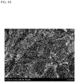
- FIGS. 3A to 3C are SEM images of the vanadium oxide-carbon based material complex prepared in Example 1, photographed at different magnifications
- FIGS. 4A to 4C are SEM images of the vanadium oxide-carbon based material complex prepared in Example 2, photographed at different magnifications
- FIGS. 5 and 6 are SEM images of the vanadium oxide-carbon based material complex prepared in Example 3 and Comparative Example 1.
- the vanadium oxide-carbon based material complexes of Examples 1 to 3 and Comparative Example 1 were found to have a laminate structure in which the carbon based material was interposed between the plate-shaped vanadium oxides.
- each of the anode materials prepared in Examples 1 and 2 was observed by electron microscopy, and elemental analysis was performed using an EDS. The results are shown in FIGS. 7 and 8 , respectively.
- the vanadium oxide-carbon based material complex having the plate-shaped laminate structure was doped with the doping element of Al or Mn (doping amount of Al in Example 1 (based on the total amount of the atoms constituting the complex): 0.3 at%, doping amount of Mn in Example 2 (based on the total amount of the atoms constituting the complex): 1.08 at%).
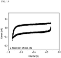
- CV curves were obtained by cyclic voltammetry (CV) for each of the compositions for forming the anode prepared in Examples 1, 2, and 4 and Comparative Examples 2 and 3.
- each of the anode materials prepared in Examples 1, 2, and 4 and Comparative Examples 2 and 3, carbon black, and PVDF as a binder were mixed at a weight ratio of 7:2:1 to prepare each of the compositions for forming the anode, and the composition was applied onto a glassy carbon electrode (GCE), and dried under vacuum and at 70 °C for 24 hours.
- GCE glassy carbon electrode
- 1 M of a Li 2 SO 4 electrolyte was impregnated into the manufactured electrode and stabilized, followed by cyclic voltammetry using a platinum counter electrode and an SCE reference electrode. At this time, the cyclic voltammetry was performed in the potential range of -1.1 V to -0.2 V at a scan rate of 10 mV/s.
- Capacitance per unit weight greatly depends on the content of vanadium oxide and the specific surface area of the anode material, and may be calculated by dividing the current values in the cyclic voltammogram by the scanning rate and the weight of the electrode active material. The results are shown in FIGS. 9 to 13 and Table 1.
- the anode materials of Examples 1, 2, and 4 exhibited high capacitance and high energy density, as compared with those of Comparative Examples 2 and 3.
- the anode materials of Examples 1 and 2 including CNT as the conductive inorganic material exhibited high capacitance of 450 F/g or more and high energy density of 50 Wh/kg or more due to high conductivity of the CNT, and capacitance of 300 F/g or more and energy density of 30 Wh/kg or more even after the 5 th cycle.
- Such excellent capacitance and energy density characteristics are attributed to the greatly increased specific surface area due to the laminate structure of the anode materials of Examples 1 and 2.
- Example 4 including graphene instead of CNT exhibited relatively low capacitance and energy density due to a low charge transfer ability and a difference of the conducting path, as compared with Examples 1 and 2.
- Comparative Example 2 not including the conductive inorganic material such as CNT exhibited very low capacitance and energy density due to a reduced charge transfer ability because of the absence of a conducting bridge which should exist between particles, as compared with the examples, and after the 5 th cycle, the difference in the capacitance and energy density was further increased.
- Comparative Example 3 including only the metal oxide-conductive inorganic material complex without the doping element exhibited very low capacitance and energy density due to a greatly reduced charge transfer ability, as compared with the examples including the doping element.
- the anode materials of Examples 1 to 3 in which the vanadium oxide-carbon based material complex was doped with Cu, Al, or Mn exhibited excellent output characteristics, as compared with the undoped anode material of Comparative Example 1. These results indicate that output characteristics of the electrode material may be further improved by doping the vanadium oxide-carbon based material complex.
- Examples 1 to 3 exhibited improved capacitance, as compared with Comparative Example 1.
- Examples 1 and 2 doped with Al or Mn exhibited greatly increased capacitance of 350 F/g or more.
- Example 3 doped with Cu exhibited low capacitance due to a relatively low charge transfer, despite metal doping, as compared with Examples 1 and 2.
Landscapes
- Engineering & Computer Science (AREA)
- Power Engineering (AREA)
- Chemical & Material Sciences (AREA)
- Microelectronics & Electronic Packaging (AREA)
- Materials Engineering (AREA)
- Manufacturing & Machinery (AREA)
- Nanotechnology (AREA)
- Crystallography & Structural Chemistry (AREA)
- Physics & Mathematics (AREA)
- General Physics & Mathematics (AREA)
- Condensed Matter Physics & Semiconductors (AREA)
- Composite Materials (AREA)
- Chemical Kinetics & Catalysis (AREA)
- Electric Double-Layer Capacitors Or The Like (AREA)
- Battery Electrode And Active Subsutance (AREA)
Applications Claiming Priority (3)
| Application Number | Priority Date | Filing Date | Title |
|---|---|---|---|
| KR20170123725 | 2017-09-25 | ||
| KR1020180113044A KR102084771B1 (ko) | 2017-09-25 | 2018-09-20 | 수도커패시터용 음극 물질 및 그 제조 방법 |
| PCT/KR2018/011263 WO2019059719A2 (fr) | 2017-09-25 | 2018-09-21 | Matériau d'électrode négative pour pseudocondensateur et son procédé de fabrication |
Publications (3)
| Publication Number | Publication Date |
|---|---|
| EP3637450A2 true EP3637450A2 (fr) | 2020-04-15 |
| EP3637450A4 EP3637450A4 (fr) | 2020-08-05 |
| EP3637450B1 EP3637450B1 (fr) | 2023-01-18 |
Family
ID=66165771
Family Applications (1)
| Application Number | Title | Priority Date | Filing Date |
|---|---|---|---|
| EP18858129.2A Active EP3637450B1 (fr) | 2017-09-25 | 2018-09-21 | Matériau d'électrode négative pour pseudocondensateur et son procédé de fabrication |
Country Status (5)
| Country | Link |
|---|---|
| US (1) | US11469055B2 (fr) |
| EP (1) | EP3637450B1 (fr) |
| JP (1) | JP6925592B2 (fr) |
| KR (1) | KR102084771B1 (fr) |
| CN (1) | CN111033660B (fr) |
Families Citing this family (6)
| Publication number | Priority date | Publication date | Assignee | Title |
|---|---|---|---|---|
| KR102301616B1 (ko) * | 2019-12-31 | 2021-09-14 | 서울대학교산학협력단 | 이차원 전이 금속 카바이드 투명 전극을 포함하는 발광 소자 및 이의 제조 방법 |
| CN113628893B (zh) * | 2021-07-16 | 2022-12-23 | 哈尔滨工程大学 | 一种高倍率、长寿命的MXene/石墨烯/碳纳米管凝胶及其制备方法和应用 |
| CN115772342A (zh) * | 2022-11-26 | 2023-03-10 | 安徽省迪盛织造整理有限公司 | MXene-石墨烯改性水性聚氨酯导电涂料的制备方法 |
| WO2025141985A1 (fr) * | 2023-12-27 | 2025-07-03 | パナソニックIpマネジメント株式会社 | Matériau feuilleté, matériau actif d'électrode pour dispositif électrochimique, dispositif électrochimique et condensateur électrochimique |
| WO2025216478A1 (fr) * | 2024-04-11 | 2025-10-16 | 한국에너지기술연구원 | Matériau composite d'électrode positive pour batterie secondaire aqueuse et procédé de fabrication associé |
| WO2026083639A1 (fr) * | 2024-10-16 | 2026-04-23 | パナソニックホールディングス株式会社 | Poudre, matériau d'électrode pour dispositif électrochimique et dispositif électrochimique |
Family Cites Families (22)
| Publication number | Priority date | Publication date | Assignee | Title |
|---|---|---|---|---|
| KR100316131B1 (ko) | 1999-09-16 | 2001-12-12 | 김선욱 | 금속산화물 의사캐패시터 |
| WO2008027502A2 (fr) | 2006-09-01 | 2008-03-06 | Battelle Memorial Institute | Nanocomposites contenant des nanotubes de carbone, procédé de fabrication de nanocomposites contenant des nanotubes de carbone, et dispositifs comprenant ces nanocomposites |
| KR20090082891A (ko) | 2006-10-18 | 2009-07-31 | 에이전시 포 사이언스, 테크놀로지 앤드 리서치 | 탄소 물질의 작용화 방법 |
| CN101064216A (zh) | 2007-05-29 | 2007-10-31 | 王国华 | 一种基于法拉第赝电容的c/v2o5超级电容器薄膜电极的制备方法 |
| US8614878B2 (en) * | 2008-01-17 | 2013-12-24 | Fraser W. SEYMOUR | Nanoscale intercalation materials on carbon powder, process for production, and use thereof |
| KR101058610B1 (ko) * | 2009-09-16 | 2011-08-22 | 삼성전기주식회사 | 금속산화물 전극물질 및 이를 이용한 전기화학적 캐패시터와 금속산화물 전극물질의 제조방법 |
| KR101280914B1 (ko) * | 2010-05-17 | 2013-07-18 | 삼화콘덴서공업주식회사 | 음극활물질 및 그 제조방법과 그 음극활물질을 포함하는 2차 전지 및 슈퍼 커패시터 |
| WO2012112818A2 (fr) | 2011-02-16 | 2012-08-23 | The Regents Of The University Of California | Réseaux interpénétrants de carbone cristallin et de matériaux électroactifs à l'échelle nanométrique |
| KR101274989B1 (ko) | 2011-09-28 | 2013-07-30 | 재단법인 포항산업과학연구원 | 도핑 탄소계 전극을 이용한 전기 이중층 커패시터 |
| WO2013070989A1 (fr) | 2011-11-10 | 2013-05-16 | The Regents Of The University Of Colorado, A Body Corporate | Dispositifs à supercondensateurs ayant des électrodes composites formées en déposant des matériaux de pseudocondensateur en oxyde de métal sur des substrats de carbone |
| KR101371288B1 (ko) | 2011-12-22 | 2014-03-07 | 이화여자대학교 산학협력단 | 망간 산화물/그래핀 나노복합체 및 이의 제조 방법 |
| JP6197454B2 (ja) | 2012-08-06 | 2017-09-20 | 東レ株式会社 | 金属酸化物ナノ粒子−導電剤複合体およびそれを用いてなるリチウムイオン二次電池及びリチウムイオンキャパシタ、ならびに金属酸化物ナノ粒子−導電剤複合体の製造方法 |
| US20140118883A1 (en) | 2012-10-31 | 2014-05-01 | Jian Xie | Graphene supported vanadium oxide monolayer capacitor material and method of making the same |
| JP6307788B2 (ja) * | 2012-12-25 | 2018-04-11 | 国立大学法人東北大学 | 導電性金属が添加された酸化物 |
| US20140248531A1 (en) * | 2013-03-01 | 2014-09-04 | Imra America, Inc. | Negative electrode active material for energy storage devices and method for making the same |
| KR101561961B1 (ko) | 2014-03-19 | 2015-10-20 | 고려대학교 산학협력단 | 전고체상 박막형 수퍼커패시터 및 그 제조 방법 |
| WO2016133571A2 (fr) | 2014-11-26 | 2016-08-25 | William Marsh Rice University | Matériaux hybrides de graphène induit par laser pour dispositifs électroniques |
| US10650984B2 (en) * | 2014-12-19 | 2020-05-12 | Nanyang Technological University | Metal oxide nanostructured material and an electrochemical cell comprising the same |
| KR101776244B1 (ko) | 2015-04-14 | 2017-09-19 | 울산과학기술원 | 복합 전극, 이의 제조 방법, 및 이를 포함하는 전기화학 소자 |
| CN105161314B (zh) * | 2015-08-26 | 2018-09-11 | 四川天策聚材科技有限公司 | 纳米氧化镍/镍/石墨烯复合材料及其制备方法和应用 |
| CN105712428B (zh) * | 2016-02-01 | 2018-07-06 | 南京理工大学 | 一种掺锑二氧化锡-碳纳米管复合吸附性电极及其制备方法 |
| CN106935419A (zh) * | 2017-04-06 | 2017-07-07 | 中国科学院山西煤炭化学研究所 | 一种钴镍双金属氧化物和石墨烯制备超级电容器电极材料的方法 |
-
2018
- 2018-09-20 KR KR1020180113044A patent/KR102084771B1/ko active Active
- 2018-09-21 US US16/627,215 patent/US11469055B2/en active Active
- 2018-09-21 CN CN201880039825.0A patent/CN111033660B/zh active Active
- 2018-09-21 EP EP18858129.2A patent/EP3637450B1/fr active Active
- 2018-09-21 JP JP2020517271A patent/JP6925592B2/ja active Active
Also Published As
| Publication number | Publication date |
|---|---|
| KR102084771B1 (ko) | 2020-03-04 |
| JP2020522900A (ja) | 2020-07-30 |
| JP6925592B2 (ja) | 2021-08-25 |
| KR20190035546A (ko) | 2019-04-03 |
| US20200279696A1 (en) | 2020-09-03 |
| US11469055B2 (en) | 2022-10-11 |
| CN111033660B (zh) | 2022-03-29 |
| EP3637450B1 (fr) | 2023-01-18 |
| EP3637450A4 (fr) | 2020-08-05 |
| CN111033660A (zh) | 2020-04-17 |
Similar Documents
| Publication | Publication Date | Title |
|---|---|---|
| EP3637450B1 (fr) | Matériau d'électrode négative pour pseudocondensateur et son procédé de fabrication | |
| Iqbal et al. | Ultrasonication-assisted synthesis of novel strontium based mixed phase structures for supercapattery devices | |
| Majumder et al. | Rare earth metal oxide (RE 2 O 3; RE= Nd, Gd, and Yb) incorporated polyindole composites: gravimetric and volumetric capacitive performance for supercapacitor applications | |
| US10003075B2 (en) | Carbon nanotube-metal nanocomposites as flexible, free standing, binder free high performance anode for Li-ion battery | |
| CN104201359B (zh) | 一种碳包覆纳米锑复合材料、其制备方法和应用 | |
| Okafor et al. | Review of advances in improving thermal, mechanical and electrochemical properties of polyaniline composite for supercapacitor application | |
| JP2012501515A (ja) | 複合電極材料と、この材料を含む電池の電極と、この電極を有するリチウム電池 | |
| US11530136B2 (en) | Preparation method of hexagonal molybdenum oxide nanorod | |
| US20080042110A1 (en) | Polyaniline/porous carbon composite and electric double layer capacitor using the same | |
| Yan et al. | Hierarchically organized CNT@ TiO 2@ Mn 3 O 4 nanostructures for enhanced lithium storage performance | |
| Tamilselvi et al. | Reduced graphene oxide (rGO): supported NiO, Co3O4 and NiCo2O4 hybrid composite on carbon cloth (CC)—bi-functional electrode/catalyst for energy storage and conversion devices | |
| Chang et al. | High-performance flexible-film supercapacitors of layered hydrous RuO2/poly (3, 4-ethylenedioxythiophene)-poly (styrenesulfonate) through vacuum filtration | |
| US12255285B2 (en) | Gel polymer electrolyte supercapacitor | |
| JP7740734B2 (ja) | 低効率正極を含む二次電池 | |
| US20230238509A1 (en) | Manufacture of electrodes for energy storage devices | |
| Mijailović et al. | Tetragonal CoMn 2 O 4 nanocrystals on electrospun carbon fibers as high-performance battery-type supercapacitor electrode materials | |
| Chen et al. | Hybridizing Fe 3 O 4 nanocrystals with nitrogen-doped carbon nanowires for high-performance supercapacitors | |
| Radhika et al. | Enhanced charge storage in ZrO2 based ternary composite electrode with superior pseudocapacitive performance | |
| WO2019059719A2 (fr) | Matériau d'électrode négative pour pseudocondensateur et son procédé de fabrication | |
| KR20230052314A (ko) | 저효율 양극을 포함하는 이차전지 | |
| US9431659B2 (en) | Electrode binder for secondary battery and electrode for secondary battery comprising the same | |
| KR101620195B1 (ko) | 주석-탄소 나노복합체 및 그 제조방법, 이를 포함하는 이차전지 | |
| Wang et al. | Multi-effect anthraquinone-based polyimide enclosed SnO2/reduced graphene oxide composite as high-performance anode for lithium-ion battery | |
| Mudila et al. | Next-generation 2D nanomaterial composites electrodes for electrochemical energy storage | |
| KR102702850B1 (ko) | 슈퍼 커패시터용 금속 복합체 및 이의 제조방법 |
Legal Events
| Date | Code | Title | Description |
|---|---|---|---|
| STAA | Information on the status of an ep patent application or granted ep patent |
Free format text: STATUS: THE INTERNATIONAL PUBLICATION HAS BEEN MADE |
|
| PUAI | Public reference made under article 153(3) epc to a published international application that has entered the european phase |
Free format text: ORIGINAL CODE: 0009012 |
|
| STAA | Information on the status of an ep patent application or granted ep patent |
Free format text: STATUS: REQUEST FOR EXAMINATION WAS MADE |
|
| 17P | Request for examination filed |
Effective date: 20200107 |
|
| AK | Designated contracting states |
Kind code of ref document: A2 Designated state(s): AL AT BE BG CH CY CZ DE DK EE ES FI FR GB GR HR HU IE IS IT LI LT LU LV MC MK MT NL NO PL PT RO RS SE SI SK SM TR |
|
| AX | Request for extension of the european patent |
Extension state: BA ME |
|
| A4 | Supplementary search report drawn up and despatched |
Effective date: 20200707 |
|
| RIC1 | Information provided on ipc code assigned before grant |
Ipc: H01G 11/50 20130101ALI20200701BHEP Ipc: H01G 11/24 20130101ALI20200701BHEP Ipc: H01G 11/02 20130101AFI20200701BHEP Ipc: H01G 11/36 20130101ALN20200701BHEP Ipc: H01G 11/46 20130101ALI20200701BHEP Ipc: H01G 11/86 20130101ALI20200701BHEP |
|
| DAV | Request for validation of the european patent (deleted) | ||
| DAX | Request for extension of the european patent (deleted) | ||
| REG | Reference to a national code |
Ref country code: DE Ref legal event code: R079 Ref document number: 602018045596 Country of ref document: DE Free format text: PREVIOUS MAIN CLASS: H01G0011460000 Ipc: H01G0011020000 |
|
| RIC1 | Information provided on ipc code assigned before grant |
Ipc: H01G 11/36 20130101ALN20220805BHEP Ipc: H01G 11/86 20130101ALI20220805BHEP Ipc: H01G 11/50 20130101ALI20220805BHEP Ipc: H01G 11/24 20130101ALI20220805BHEP Ipc: H01G 11/46 20130101ALI20220805BHEP Ipc: H01G 11/02 20130101AFI20220805BHEP |
|
| GRAP | Despatch of communication of intention to grant a patent |
Free format text: ORIGINAL CODE: EPIDOSNIGR1 |
|
| STAA | Information on the status of an ep patent application or granted ep patent |
Free format text: STATUS: GRANT OF PATENT IS INTENDED |
|
| INTG | Intention to grant announced |
Effective date: 20220916 |
|
| GRAS | Grant fee paid |
Free format text: ORIGINAL CODE: EPIDOSNIGR3 |
|
| GRAA | (expected) grant |
Free format text: ORIGINAL CODE: 0009210 |
|
| STAA | Information on the status of an ep patent application or granted ep patent |
Free format text: STATUS: THE PATENT HAS BEEN GRANTED |
|
| AK | Designated contracting states |
Kind code of ref document: B1 Designated state(s): AL AT BE BG CH CY CZ DE DK EE ES FI FR GB GR HR HU IE IS IT LI LT LU LV MC MK MT NL NO PL PT RO RS SE SI SK SM TR |
|
| REG | Reference to a national code |
Ref country code: GB Ref legal event code: FG4D |
|
| REG | Reference to a national code |
Ref country code: CH Ref legal event code: EP |
|
| REG | Reference to a national code |
Ref country code: AT Ref legal event code: REF Ref document number: 1545142 Country of ref document: AT Kind code of ref document: T Effective date: 20230215 Ref country code: IE Ref legal event code: FG4D |
|
| REG | Reference to a national code |
Ref country code: DE Ref legal event code: R096 Ref document number: 602018045596 Country of ref document: DE |
|
| REG | Reference to a national code |
Ref country code: LT Ref legal event code: MG9D |
|
| REG | Reference to a national code |
Ref country code: NL Ref legal event code: MP Effective date: 20230118 |
|
| REG | Reference to a national code |
Ref country code: AT Ref legal event code: MK05 Ref document number: 1545142 Country of ref document: AT Kind code of ref document: T Effective date: 20230118 |
|
| PG25 | Lapsed in a contracting state [announced via postgrant information from national office to epo] |
Ref country code: NL Free format text: LAPSE BECAUSE OF FAILURE TO SUBMIT A TRANSLATION OF THE DESCRIPTION OR TO PAY THE FEE WITHIN THE PRESCRIBED TIME-LIMIT Effective date: 20230118 |
|
| PG25 | Lapsed in a contracting state [announced via postgrant information from national office to epo] |
Ref country code: RS Free format text: LAPSE BECAUSE OF FAILURE TO SUBMIT A TRANSLATION OF THE DESCRIPTION OR TO PAY THE FEE WITHIN THE PRESCRIBED TIME-LIMIT Effective date: 20230118 Ref country code: PT Free format text: LAPSE BECAUSE OF FAILURE TO SUBMIT A TRANSLATION OF THE DESCRIPTION OR TO PAY THE FEE WITHIN THE PRESCRIBED TIME-LIMIT Effective date: 20230518 Ref country code: NO Free format text: LAPSE BECAUSE OF FAILURE TO SUBMIT A TRANSLATION OF THE DESCRIPTION OR TO PAY THE FEE WITHIN THE PRESCRIBED TIME-LIMIT Effective date: 20230418 Ref country code: LV Free format text: LAPSE BECAUSE OF FAILURE TO SUBMIT A TRANSLATION OF THE DESCRIPTION OR TO PAY THE FEE WITHIN THE PRESCRIBED TIME-LIMIT Effective date: 20230118 Ref country code: LT Free format text: LAPSE BECAUSE OF FAILURE TO SUBMIT A TRANSLATION OF THE DESCRIPTION OR TO PAY THE FEE WITHIN THE PRESCRIBED TIME-LIMIT Effective date: 20230118 Ref country code: HR Free format text: LAPSE BECAUSE OF FAILURE TO SUBMIT A TRANSLATION OF THE DESCRIPTION OR TO PAY THE FEE WITHIN THE PRESCRIBED TIME-LIMIT Effective date: 20230118 Ref country code: ES Free format text: LAPSE BECAUSE OF FAILURE TO SUBMIT A TRANSLATION OF THE DESCRIPTION OR TO PAY THE FEE WITHIN THE PRESCRIBED TIME-LIMIT Effective date: 20230118 Ref country code: AT Free format text: LAPSE BECAUSE OF FAILURE TO SUBMIT A TRANSLATION OF THE DESCRIPTION OR TO PAY THE FEE WITHIN THE PRESCRIBED TIME-LIMIT Effective date: 20230118 |
|
| PG25 | Lapsed in a contracting state [announced via postgrant information from national office to epo] |
Ref country code: SE Free format text: LAPSE BECAUSE OF FAILURE TO SUBMIT A TRANSLATION OF THE DESCRIPTION OR TO PAY THE FEE WITHIN THE PRESCRIBED TIME-LIMIT Effective date: 20230118 Ref country code: PL Free format text: LAPSE BECAUSE OF FAILURE TO SUBMIT A TRANSLATION OF THE DESCRIPTION OR TO PAY THE FEE WITHIN THE PRESCRIBED TIME-LIMIT Effective date: 20230118 Ref country code: IS Free format text: LAPSE BECAUSE OF FAILURE TO SUBMIT A TRANSLATION OF THE DESCRIPTION OR TO PAY THE FEE WITHIN THE PRESCRIBED TIME-LIMIT Effective date: 20230518 Ref country code: GR Free format text: LAPSE BECAUSE OF FAILURE TO SUBMIT A TRANSLATION OF THE DESCRIPTION OR TO PAY THE FEE WITHIN THE PRESCRIBED TIME-LIMIT Effective date: 20230419 Ref country code: FI Free format text: LAPSE BECAUSE OF FAILURE TO SUBMIT A TRANSLATION OF THE DESCRIPTION OR TO PAY THE FEE WITHIN THE PRESCRIBED TIME-LIMIT Effective date: 20230118 |
|
| REG | Reference to a national code |
Ref country code: DE Ref legal event code: R097 Ref document number: 602018045596 Country of ref document: DE |
|
| PG25 | Lapsed in a contracting state [announced via postgrant information from national office to epo] |
Ref country code: SM Free format text: LAPSE BECAUSE OF FAILURE TO SUBMIT A TRANSLATION OF THE DESCRIPTION OR TO PAY THE FEE WITHIN THE PRESCRIBED TIME-LIMIT Effective date: 20230118 Ref country code: RO Free format text: LAPSE BECAUSE OF FAILURE TO SUBMIT A TRANSLATION OF THE DESCRIPTION OR TO PAY THE FEE WITHIN THE PRESCRIBED TIME-LIMIT Effective date: 20230118 Ref country code: EE Free format text: LAPSE BECAUSE OF FAILURE TO SUBMIT A TRANSLATION OF THE DESCRIPTION OR TO PAY THE FEE WITHIN THE PRESCRIBED TIME-LIMIT Effective date: 20230118 Ref country code: DK Free format text: LAPSE BECAUSE OF FAILURE TO SUBMIT A TRANSLATION OF THE DESCRIPTION OR TO PAY THE FEE WITHIN THE PRESCRIBED TIME-LIMIT Effective date: 20230118 Ref country code: CZ Free format text: LAPSE BECAUSE OF FAILURE TO SUBMIT A TRANSLATION OF THE DESCRIPTION OR TO PAY THE FEE WITHIN THE PRESCRIBED TIME-LIMIT Effective date: 20230118 |
|
| PLBE | No opposition filed within time limit |
Free format text: ORIGINAL CODE: 0009261 |
|
| STAA | Information on the status of an ep patent application or granted ep patent |
Free format text: STATUS: NO OPPOSITION FILED WITHIN TIME LIMIT |
|
| PG25 | Lapsed in a contracting state [announced via postgrant information from national office to epo] |
Ref country code: SK Free format text: LAPSE BECAUSE OF FAILURE TO SUBMIT A TRANSLATION OF THE DESCRIPTION OR TO PAY THE FEE WITHIN THE PRESCRIBED TIME-LIMIT Effective date: 20230118 |
|
| 26N | No opposition filed |
Effective date: 20231019 |
|
| PG25 | Lapsed in a contracting state [announced via postgrant information from national office to epo] |
Ref country code: SI Free format text: LAPSE BECAUSE OF FAILURE TO SUBMIT A TRANSLATION OF THE DESCRIPTION OR TO PAY THE FEE WITHIN THE PRESCRIBED TIME-LIMIT Effective date: 20230118 |
|
| REG | Reference to a national code |
Ref country code: CH Ref legal event code: PL |
|
| PG25 | Lapsed in a contracting state [announced via postgrant information from national office to epo] |
Ref country code: LU Free format text: LAPSE BECAUSE OF NON-PAYMENT OF DUE FEES Effective date: 20230921 |
|
| REG | Reference to a national code |
Ref country code: BE Ref legal event code: MM Effective date: 20230930 |
|
| PG25 | Lapsed in a contracting state [announced via postgrant information from national office to epo] |
Ref country code: LU Free format text: LAPSE BECAUSE OF NON-PAYMENT OF DUE FEES Effective date: 20230921 Ref country code: IT Free format text: LAPSE BECAUSE OF FAILURE TO SUBMIT A TRANSLATION OF THE DESCRIPTION OR TO PAY THE FEE WITHIN THE PRESCRIBED TIME-LIMIT Effective date: 20230118 Ref country code: MC Free format text: LAPSE BECAUSE OF FAILURE TO SUBMIT A TRANSLATION OF THE DESCRIPTION OR TO PAY THE FEE WITHIN THE PRESCRIBED TIME-LIMIT Effective date: 20230118 |
|
| REG | Reference to a national code |
Ref country code: IE Ref legal event code: MM4A |
|
| PG25 | Lapsed in a contracting state [announced via postgrant information from national office to epo] |
Ref country code: IE Free format text: LAPSE BECAUSE OF NON-PAYMENT OF DUE FEES Effective date: 20230921 |
|
| PG25 | Lapsed in a contracting state [announced via postgrant information from national office to epo] |
Ref country code: CH Free format text: LAPSE BECAUSE OF NON-PAYMENT OF DUE FEES Effective date: 20230930 |
|
| PG25 | Lapsed in a contracting state [announced via postgrant information from national office to epo] |
Ref country code: IE Free format text: LAPSE BECAUSE OF NON-PAYMENT OF DUE FEES Effective date: 20230921 Ref country code: CH Free format text: LAPSE BECAUSE OF NON-PAYMENT OF DUE FEES Effective date: 20230930 |
|
| PG25 | Lapsed in a contracting state [announced via postgrant information from national office to epo] |
Ref country code: BE Free format text: LAPSE BECAUSE OF NON-PAYMENT OF DUE FEES Effective date: 20230930 |
|
| PG25 | Lapsed in a contracting state [announced via postgrant information from national office to epo] |
Ref country code: BG Free format text: LAPSE BECAUSE OF FAILURE TO SUBMIT A TRANSLATION OF THE DESCRIPTION OR TO PAY THE FEE WITHIN THE PRESCRIBED TIME-LIMIT Effective date: 20230118 |
|
| PG25 | Lapsed in a contracting state [announced via postgrant information from national office to epo] |
Ref country code: BG Free format text: LAPSE BECAUSE OF FAILURE TO SUBMIT A TRANSLATION OF THE DESCRIPTION OR TO PAY THE FEE WITHIN THE PRESCRIBED TIME-LIMIT Effective date: 20230118 |
|
| PG25 | Lapsed in a contracting state [announced via postgrant information from national office to epo] |
Ref country code: CY Free format text: LAPSE BECAUSE OF FAILURE TO SUBMIT A TRANSLATION OF THE DESCRIPTION OR TO PAY THE FEE WITHIN THE PRESCRIBED TIME-LIMIT; INVALID AB INITIO Effective date: 20180921 |
|
| PG25 | Lapsed in a contracting state [announced via postgrant information from national office to epo] |
Ref country code: HU Free format text: LAPSE BECAUSE OF FAILURE TO SUBMIT A TRANSLATION OF THE DESCRIPTION OR TO PAY THE FEE WITHIN THE PRESCRIBED TIME-LIMIT; INVALID AB INITIO Effective date: 20180921 |
|
| PGFP | Annual fee paid to national office [announced via postgrant information from national office to epo] |
Ref country code: DE Payment date: 20250820 Year of fee payment: 8 |
|
| PGFP | Annual fee paid to national office [announced via postgrant information from national office to epo] |
Ref country code: GB Payment date: 20250820 Year of fee payment: 8 |
|
| PGFP | Annual fee paid to national office [announced via postgrant information from national office to epo] |
Ref country code: FR Payment date: 20250821 Year of fee payment: 8 |
|
| PG25 | Lapsed in a contracting state [announced via postgrant information from national office to epo] |
Ref country code: TR Free format text: LAPSE BECAUSE OF FAILURE TO SUBMIT A TRANSLATION OF THE DESCRIPTION OR TO PAY THE FEE WITHIN THE PRESCRIBED TIME-LIMIT Effective date: 20230118 |