EP3637472B1 - Organic light emitting diode display panels and display devices including the same - Google Patents
Organic light emitting diode display panels and display devices including the same Download PDFInfo
- Publication number
- EP3637472B1 EP3637472B1 EP19200233.5A EP19200233A EP3637472B1 EP 3637472 B1 EP3637472 B1 EP 3637472B1 EP 19200233 A EP19200233 A EP 19200233A EP 3637472 B1 EP3637472 B1 EP 3637472B1
- Authority
- EP
- European Patent Office
- Prior art keywords
- oled
- display panel
- visible light
- light
- oled display
- Prior art date
- Legal status (The legal status is an assumption and is not a legal conclusion. Google has not performed a legal analysis and makes no representation as to the accuracy of the status listed.)
- Active
Links
Images







Classifications
-
- G—PHYSICS
- G06—COMPUTING OR CALCULATING; COUNTING
- G06F—ELECTRIC DIGITAL DATA PROCESSING
- G06F21/00—Security arrangements for protecting computers, components thereof, programs or data against unauthorised activity
- G06F21/30—Authentication, i.e. establishing the identity or authorisation of security principals
- G06F21/31—User authentication
- G06F21/32—User authentication using biometric data, e.g. fingerprints, iris scans or voiceprints
-
- H—ELECTRICITY
- H10—SEMICONDUCTOR DEVICES; ELECTRIC SOLID-STATE DEVICES NOT OTHERWISE PROVIDED FOR
- H10K—ORGANIC ELECTRIC SOLID-STATE DEVICES
- H10K59/00—Integrated devices, or assemblies of multiple devices, comprising at least one organic light-emitting element covered by group H10K50/00
- H10K59/60—OLEDs integrated with inorganic light-sensitive elements, e.g. with inorganic solar cells or inorganic photodiodes
-
- G—PHYSICS
- G06—COMPUTING OR CALCULATING; COUNTING
- G06F—ELECTRIC DIGITAL DATA PROCESSING
- G06F3/00—Input arrangements for transferring data to be processed into a form capable of being handled by the computer; Output arrangements for transferring data from processing unit to output unit, e.g. interface arrangements
- G06F3/01—Input arrangements or combined input and output arrangements for interaction between user and computer
- G06F3/03—Arrangements for converting the position or the displacement of a member into a coded form
- G06F3/041—Digitisers, e.g. for touch screens or touch pads, characterised by the transducing means
- G06F3/0412—Digitisers structurally integrated in a display
-
- G—PHYSICS
- G06—COMPUTING OR CALCULATING; COUNTING
- G06V—IMAGE OR VIDEO RECOGNITION OR UNDERSTANDING
- G06V10/00—Arrangements for image or video recognition or understanding
- G06V10/10—Image acquisition
- G06V10/12—Details of acquisition arrangements; Constructional details thereof
- G06V10/14—Optical characteristics of the device performing the acquisition or on the illumination arrangements
- G06V10/143—Sensing or illuminating at different wavelengths
-
- G—PHYSICS
- G06—COMPUTING OR CALCULATING; COUNTING
- G06V—IMAGE OR VIDEO RECOGNITION OR UNDERSTANDING
- G06V40/00—Recognition of biometric, human-related or animal-related patterns in image or video data
- G06V40/10—Human or animal bodies, e.g. vehicle occupants or pedestrians; Body parts, e.g. hands
- G06V40/12—Fingerprints or palmprints
- G06V40/13—Sensors therefor
- G06V40/1318—Sensors therefor using electro-optical elements or layers, e.g. electroluminescent sensing
-
- H—ELECTRICITY
- H10—SEMICONDUCTOR DEVICES; ELECTRIC SOLID-STATE DEVICES NOT OTHERWISE PROVIDED FOR
- H10F—INORGANIC SEMICONDUCTOR DEVICES SENSITIVE TO INFRARED RADIATION, LIGHT, ELECTROMAGNETIC RADIATION OF SHORTER WAVELENGTH OR CORPUSCULAR RADIATION
- H10F30/00—Individual radiation-sensitive semiconductor devices in which radiation controls the flow of current through the devices, e.g. photodetectors
- H10F30/20—Individual radiation-sensitive semiconductor devices in which radiation controls the flow of current through the devices, e.g. photodetectors the devices having potential barriers, e.g. phototransistors
- H10F30/21—Individual radiation-sensitive semiconductor devices in which radiation controls the flow of current through the devices, e.g. photodetectors the devices having potential barriers, e.g. phototransistors the devices being sensitive to infrared, visible or ultraviolet radiation
- H10F30/22—Individual radiation-sensitive semiconductor devices in which radiation controls the flow of current through the devices, e.g. photodetectors the devices having potential barriers, e.g. phototransistors the devices being sensitive to infrared, visible or ultraviolet radiation the devices having only one potential barrier, e.g. photodiodes
- H10F30/223—Individual radiation-sensitive semiconductor devices in which radiation controls the flow of current through the devices, e.g. photodetectors the devices having potential barriers, e.g. phototransistors the devices being sensitive to infrared, visible or ultraviolet radiation the devices having only one potential barrier, e.g. photodiodes the potential barrier being a PIN barrier
-
- H—ELECTRICITY
- H10—SEMICONDUCTOR DEVICES; ELECTRIC SOLID-STATE DEVICES NOT OTHERWISE PROVIDED FOR
- H10K—ORGANIC ELECTRIC SOLID-STATE DEVICES
- H10K39/00—Integrated devices, or assemblies of multiple devices, comprising at least one organic radiation-sensitive element covered by group H10K30/00
- H10K39/30—Devices controlled by radiation
- H10K39/32—Organic image sensors
-
- H—ELECTRICITY
- H10—SEMICONDUCTOR DEVICES; ELECTRIC SOLID-STATE DEVICES NOT OTHERWISE PROVIDED FOR
- H10K—ORGANIC ELECTRIC SOLID-STATE DEVICES
- H10K59/00—Integrated devices, or assemblies of multiple devices, comprising at least one organic light-emitting element covered by group H10K50/00
- H10K59/10—OLED displays
- H10K59/12—Active-matrix OLED [AMOLED] displays
-
- H—ELECTRICITY
- H10—SEMICONDUCTOR DEVICES; ELECTRIC SOLID-STATE DEVICES NOT OTHERWISE PROVIDED FOR
- H10K—ORGANIC ELECTRIC SOLID-STATE DEVICES
- H10K59/00—Integrated devices, or assemblies of multiple devices, comprising at least one organic light-emitting element covered by group H10K50/00
- H10K59/30—Devices specially adapted for multicolour light emission
- H10K59/35—Devices specially adapted for multicolour light emission comprising red-green-blue [RGB] subpixels
-
- H—ELECTRICITY
- H10—SEMICONDUCTOR DEVICES; ELECTRIC SOLID-STATE DEVICES NOT OTHERWISE PROVIDED FOR
- H10K—ORGANIC ELECTRIC SOLID-STATE DEVICES
- H10K59/00—Integrated devices, or assemblies of multiple devices, comprising at least one organic light-emitting element covered by group H10K50/00
- H10K59/30—Devices specially adapted for multicolour light emission
- H10K59/35—Devices specially adapted for multicolour light emission comprising red-green-blue [RGB] subpixels
- H10K59/351—Devices specially adapted for multicolour light emission comprising red-green-blue [RGB] subpixels comprising more than three subpixels, e.g. red-green-blue-white [RGBW]
-
- H—ELECTRICITY
- H10—SEMICONDUCTOR DEVICES; ELECTRIC SOLID-STATE DEVICES NOT OTHERWISE PROVIDED FOR
- H10K—ORGANIC ELECTRIC SOLID-STATE DEVICES
- H10K59/00—Integrated devices, or assemblies of multiple devices, comprising at least one organic light-emitting element covered by group H10K50/00
- H10K59/30—Devices specially adapted for multicolour light emission
- H10K59/35—Devices specially adapted for multicolour light emission comprising red-green-blue [RGB] subpixels
- H10K59/353—Devices specially adapted for multicolour light emission comprising red-green-blue [RGB] subpixels characterised by the geometrical arrangement of the RGB subpixels
-
- H—ELECTRICITY
- H10—SEMICONDUCTOR DEVICES; ELECTRIC SOLID-STATE DEVICES NOT OTHERWISE PROVIDED FOR
- H10K—ORGANIC ELECTRIC SOLID-STATE DEVICES
- H10K59/00—Integrated devices, or assemblies of multiple devices, comprising at least one organic light-emitting element covered by group H10K50/00
- H10K59/40—OLEDs integrated with touch screens
-
- H—ELECTRICITY
- H10—SEMICONDUCTOR DEVICES; ELECTRIC SOLID-STATE DEVICES NOT OTHERWISE PROVIDED FOR
- H10K—ORGANIC ELECTRIC SOLID-STATE DEVICES
- H10K59/00—Integrated devices, or assemblies of multiple devices, comprising at least one organic light-emitting element covered by group H10K50/00
- H10K59/60—OLEDs integrated with inorganic light-sensitive elements, e.g. with inorganic solar cells or inorganic photodiodes
- H10K59/65—OLEDs integrated with inorganic image sensors
-
- H—ELECTRICITY
- H10—SEMICONDUCTOR DEVICES; ELECTRIC SOLID-STATE DEVICES NOT OTHERWISE PROVIDED FOR
- H10K—ORGANIC ELECTRIC SOLID-STATE DEVICES
- H10K59/00—Integrated devices, or assemblies of multiple devices, comprising at least one organic light-emitting element covered by group H10K50/00
- H10K59/80—Constructional details
- H10K59/805—Electrodes
-
- H—ELECTRICITY
- H10—SEMICONDUCTOR DEVICES; ELECTRIC SOLID-STATE DEVICES NOT OTHERWISE PROVIDED FOR
- H10K—ORGANIC ELECTRIC SOLID-STATE DEVICES
- H10K77/00—Constructional details of devices covered by this subclass and not covered by groups H10K10/80, H10K30/80, H10K50/80 or H10K59/80
-
- G—PHYSICS
- G09—EDUCATION; CRYPTOGRAPHY; DISPLAY; ADVERTISING; SEALS
- G09G—ARRANGEMENTS OR CIRCUITS FOR CONTROL OF INDICATING DEVICES USING STATIC MEANS TO PRESENT VARIABLE INFORMATION
- G09G2360/00—Aspects of the architecture of display systems
- G09G2360/14—Detecting light within display terminals, e.g. using a single or a plurality of photosensors
- G09G2360/145—Detecting light within display terminals, e.g. using a single or a plurality of photosensors the light originating from the display screen
- G09G2360/147—Detecting light within display terminals, e.g. using a single or a plurality of photosensors the light originating from the display screen the originated light output being determined for each pixel
Definitions
- This disclosure relates to organic light emitting diode display panels and display devices including the same, and more particularly to visible light sensor embedded organic light emitting diode display panels configured to implement biometric recognition and devices including the same.
- OLED display panels have merits of excellent luminance, driving voltage, and response rate characteristics and implementing color images, so they are being employed for various display devices.
- biometric recognition technologies via which certain biometric information or gesture information is extracted by one or more devices to authenticate a person in financial, health care, and mobile fields.
- leading smartphone companies are focusing on adapting fingerprint and iris recognition technologies.
- US 2015-0331508 discloses technologies of forming a near-infrared sensor for fingerprint recognition on the same plane as an OLED emitter. That is, a separate near-infrared emitter and near-infrared detector are utilized for fingerprint recognition.
- an aperture ratio of the OLED emitter including such near-infrared emitter and the near-infrared detector may be decreased compared with a conventional OLED emitter having no near-infrared emitter and near-infrared detector.
- the aperture ratio decrease of the OLED emitter may have a large influence on display characteristics of a mobile display device including the OLED emitter, particularly, a smart phone having a small display area.
- US 2018/158877 discloses a display panel comprising a substrate, OLED light emitting structures, and fingerprint recognitions units.
- US 2018/101271 discloses a biometric-recognition display panel comprising sensing circuits for sensing an intensity of light from an emitting device.
- US 2013/278577 discloses a sensing device including a light sensor located in at least one of an upper and a lower panel, as well as a backlight device including light emitting members.
- US 6 747 290 B2 discloses a display device in an information device having a pen input function.
- Some example embodiments provide a visible light sensor embedded OLED display panel as defined by claim 1 (also referred to herein as simply an "OLED display panel") configured to implement biometric recognition without an effect on an aperture ratio of an OLED emitter or reducing or minimizing the effect, thereby improving performance of the OLED display panel, for example improving the display characteristics of a display device including the OLED display panel.
- OLED display panel also referred to herein as simply an "OLED display panel”
- Some example embodiments provide a display device that includes a visible light sensor embedded OLED display panel as defined by claim 1 configured to implement biometric recognition without an effect on an aperture ratio of an OLED display part or reducing or minimizing the effect, thereby improving performance of the OLED display panel, for example improving the display characteristics of a display device including the OLED display panel.
- An OLED display panel as defined in claim 1, according to some example embodiments is configured to display images and to emit light for biometric recognition; and a visible light sensor configured to detect light reflected by a recognition target after being emitted by the OLED light emitter, wherein the visible light sensor is positioned under a non-light emitting region of the OLED light emitter.
- the OLED display panel may be configured to perform biometric recognition without a separate light source other than the OLED light emitter, so as to prevent an aperture ratio decrease of the OLED light emitter.
- the OLED display panel may maintain the aperture ratio of the OLED light emitter at about 100 % or may reduce or minimize the aperture ratio decrease by forming the visible light sensor in a non-light emitting region that does not affect the aperture ratio of the OLED light emitter based on the location of the visible light sensor, or by forming the visible light sensor in a stack structure under the non-light emitting region (e.g., between the non-light emitting region of the OLED light emitter and a substrate).
- Accuracy or efficiency of biometric recognition provided by the aforementioned OLED display panels may be improved since the amount or intensity of the light emitted to perform biometric recognition is increased or maximized based on employing the biometric recognition sensor as a visible light sensor.
- the visible light sensor may be formed of (e.g., may at least partially comprise) an organic material and thus may be bent or stretchable. Accordingly, the visible light sensor may contribute to easily realizing a flexible display device and thus improve portability and versatility of a display device that includes the OLED display panel.
- an OLED display according to claim 1.
- the visible light sensor may be configured to absorb light in an entirety of a wavelength spectrum of visible light.
- the visible light sensor may include an organic photodiode including an organic material.
- the visible light sensor may include an a-Si-based P-I-N photodiode, a poly-Si-based P-I-N photodiode, a CIGS (Cu-In-Ga-Se) photodiode, or a Cd-Te photodiode.
- the driving the OLED light emitter may include selectively driving a particular limited set of OLED light emitters of an array of OLED light emitters of the OLED display panel.
- the further driving the visible light sensor may include selectively driving a particular limited set of visible light sensors of an array of visible light sensors of the OLED display panel.
- the OLED display panel may further include an infrared light emitter on the substrate, the infrared light emitter configured to emit infrared light, and an infrared light sensor on the substrate, the infrared light sensor configured to detect at least a portion of the emitted infrared light based on reflection of the portion of the emitted infrared light from a recognition target.
- the infrared light sensor may be in a separate non-light emitting region adjacent to the OLED light emitter, or between the substrate and a separate non-light emitting region that is adjacent to the OLED light emitter.
- the array of infrared light emitters and the array of infrared light sensors may not extend through the third region.
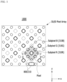
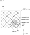
- FIG. 1 shows a pentile matrix type layout in which one pixel (Px) comprises two green sub-pixels 310G, one red sub-pixel 310R, and one blue sub-pixel 310B (e.g., RGBG).
- sub-pixel 310R may be referred to as a red OLED sub-pixel
- sub-pixel 310G may be referred to as a green OLED sub-pixel
- sub-pixel 310B may be referred to as a blue OLED sub-pixel.
- the pixel array of the OLED display panel 1000 includes an array of red sub-pixels 310R, an array of blue sub-pixels 310B, and an array of green sub-pixels 310G. As shown, each array defines a separate pattern of the respective sub-pixels 310R, 310B, 310G, where some or all of the sub-pixels in a given pattern of sub-pixels may include a particular type of sub-pixel 310R, 310B, 310G. It will be understood that a given sub-pixel 310R, 310G, 310B that is defined by a pattern of respective OLEDs may not include an OLED 310 that corresponds to the sub-pixel.
- a visible light sensor 210 may replace an OLED 310 in a given sub-pixel that corresponds to a pattern of OLEDS 310 (e.g., the visible light sensor 210 may be in a position at which an OLED 310 should otherwise be located based on a pattern of other OLEDs configured to emit the same wavelength spectrum of light) such that the visible light sensor 210 may be referred to as being "in" the given sub-pixel, provided that it is arranged as defined in claim 1.
- the OLEDs 310 are spaced apart from each other in a horizontal direction that is parallel to the upper surface 110u of the substrate 110 (e.g., an x-direction and/or a y-direction).
- the regions adjacent to the OLEDs 310 in the OLED light emitter stack 300 may be referred to as non-light emitting regions 800 of the OLED light emitter stack 300, and thus each unit pixel (Px) includes OLEDs 310 and a non-light emitting region 800 adjacent to the one or more OLEDs 310.
- the non-light-emitting region of a unit pixel (Px) may be a continuous region that surrounds the OLEDs 310 of the pixels (Px) of the OLED display panel 1000 in the pixel array of the OLED display panel 1000.
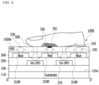
- the non-light emitting region(s) of the OLED display panel 1000 may include insulating layers 350 and 360, which may be at least partially transparent to light 330 that may be emitted by the OLEDs 310 and reflected back into and through the OLED light emitter stack 300 from a recognition target. Accordingly, reflected light 245 may pass through the OLED light emitter stack 300 via the non-light emitting region(s) of the unit pixels (Px) of the OLED display panel 1000.
- the unit pixels (Px) of the OLED display panel 1000 may have the same horizontal boundaries (e.g., in the x and y directions) as the corresponding unit pixels (Px) of the OLED light emitter stack 300, where the unit pixels (Px) of the OLED light emitter stack 300 are defined by a particular grouping of the sub-pixels 310R, 310G, 310B of the OLED light emitter stack 300, the unit pixels (Px) of the OLED display panel 1000 and the corresponding unit pixels (Px) of the OLED light emitter stack 300 may be collectively referred to herein as simply unit pixels (Px) or simply pixels (Px).
- some or all of the pixels (Px) and/or sub-pixels in the OLED display panel 1000 and/or OLED light emitter stack 300 may be arranged according to one or more other patterns, or matrices, including a strip structure pattern.
- each pixel (Px) of the OLED display panel 1000 may be described as including an array of pixels (Px), where each pixel (Px) of the OLED display panel 1000 may be considered to correspond to a separate pixel (Px) of the OLED light emitter stack 300. Additionally, each pixel (Px) of the OLED display panel 1000 includes sub-pixels (Sub-Px), where each sub-pixel (Sub-Px) of a pixel (Px) of the OLED display panel 1000 is considered to correspond to a separate sub-pixel 310R, 310G, 310B of the OLED light emitter stack 300. For example, as shown in FIG.
- a given pixel (Px) of the OLED light emitter stack 300 includes a certain set of sub-pixels 310R, 310G, and 310B that are configured to emit light having different wavelength spectra ( one red sub-pixel 310R, one blue sub-pixel 310B, and two green sub-pixels 310G may define a pixel (Px) of the OLED light emitter stack 300), and a given pixel (Px) of the OLED display panel 1000 encompasses (and is defined by) the given pixel (Px) of the OLED light emitter stack 300, such that the given pixel (Px) of the OLED display panel includes (and is defined by) the given pixel of the OLED light emitter stack 300 and the portions of the visible light sensor stack 200, driver 100, substrate 110, and cover glass 450 that overlap the pixel (Px) of the OLED light emitter stack 300.
- each separate sub-pixel (Sub-Px) of the given pixel (Px) of the OLED display panel 1000 includes (and is defined by) a separate sub-pixel 310R, 310B, 310G of the pixel (Px) of the OLED light emitter stack 300 and further includes the portions of the visible light sensor stack 200, driver 100, substrate 110, and cover glass 450 that overlap the respective sub-pixel of the OLED light emitter stack 300.
- each sub-pixel of the OLED display panel 1000 includes a respective sub-pixel of the OLED light emitter stack 300 and also includes a portion (e.g., half) of the non-light emitting region 800 extending between the respective sub-pixel of the OLED light emitter stack 300 and one or more adjacent sub-pixels of the OLED light emitter stack 300.
- OLED display panel 1000 includes a given pixel (Px) of the OLED light emitting stack.
- OLED sub-pixels are referenced, it will be understood that said OLED sub-pixels are referring to sub-pixels of the OLED light emitter stack 300 (e.g., 310R, 310G, 310B), instead of sub-pixels of the OLED display panel 1000.
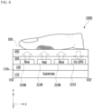
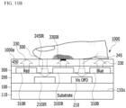
- a visible light sensor 210 is disposed under the non-light emitting region 800 to implement the detection of the visible light 245 received at the visible light sensor 210 through the non-light emitting region 800 between respective OLED sub-pixels (Sub-Px).
- FIG. 2 shows one example that the sub-pixels 310R, 310G, and 310B and the visible light sensor 210 are partially overlapped in the vertical direction (z-direction). Accordingly, as shown in FIGS.
- a visible light sensor 210 is between a non-light emitting region 800 of the OLED light emitter stack 300 and the substrate 110 so as to be vertically aligned with the non-light emitting region 800 of the OLED light emitter stack 300 in a vertical direction (e.g., Z-direction) extending perpendicular to the upper surface 110u of the substrate 110.
- an element that is “above” or “below” another element may be referred to as being “on” the other element.
- an element that is described herein to be “on” another element may be “above” or “below” the other element.
- an element that is described to be “between” two other elements may be separately “on” each of the two other elements.
- an element that is “on” another element may be “directly” on the other element so as to be in direct contact with the other element or may be “indirectly” on the other element so as to be isolated from direct contact with the other element by one or more interposing spaces and/or structures.
- an element and/or direction that is described herein as being parallel with a reference surface may be substantially parallel with the reference surface such that the element and/or direction is parallel with the reference surface within manufacturing tolerances and/or material tolerances. It will be understood that an element and/or direction that is described herein as being perpendicular with a reference surface may be substantially perpendicular with the reference surface such that the element and/or direction is perpendicular with the reference surface within manufacturing tolerances and/or material tolerances.
- the OLED display panel 1000 shown in FIGS. 1 and 2 may be suitable for a high resolution display panel having a display resolution of greater than or equal to about 2960X1440 (WQHD) and an aperture ratio between sub-pixels (Sub-Px) of about 4 %. But the present disclosure is not necessarily limited to the resolution and the aperture ratio.
- the OLED light emitter stack 300 is a region configured to emit light, and therefore is configured to emit light to display an image and also to emit light for biometric recognition, simultaneously or separately.
- the OLED light emitter stack 300 includes OLEDs 310 (also referred to herein as OLED light emitters), each OLED 310 including an organic emission layer 311, and a first electrode 313 and a second electrode 315 formed under and on the organic emission layer 311.
- the OLED light emitter stack 300 includes insulation layers 350 and 360, where portions of the OLEDs 310 may be formed on insulation layer 350, in gaps in the insulation layer 350, and/or between separate instances of insulation layer 350, and insulation layer 360 may be formed on both insulation layer 350 and the OLEDs 310 to cover the OLEDs 310.
- the organic emission layer 311 may be formed of (may at least partially comprise) various organic materials inherently configured to emit light 330 of any one of red R, green G, and blue B colors (wavelength spectra) away from an upper surface 110u of the substrate 110, that is, in an opposite direction from the visible light sensor stack 200. Accordingly, and as shown in FIG. 1 , each separate OLED 310 in a unit pixel (Px) of the OLED light emitter stack 300 (and thus a unit pixel (Px) of the OLED display panel 1000) may be considered to be, and thus may define, a separate sub-pixel 310R, 310B, 310G of the OLED light emitter stack 300 (OLED sub-pixel).
- the second electrode 315 may be formed as a light-transmitting electrode with a thickness of less than or equal to about 100 nm.
- the second electrode 315 may be formed of MgAg, Ag, Mg, Al, Mo, Ti, TiN, Ni, ITO, IZO, AlZO, AlTO, or the like.
- the first electrode 313 may be formed with a reflecting electrode.
- the first electrode 313 may be formed of Al, Ag. Mo, AlNd, Mo/Al/Mo, TiN, ITO/Ag/ITO, ITO/Al/ITO, ITO/Mo/ITO, or the like. It may be formed with a light transmitting electrode to fluently enter light toward the lower visible light sensor stack 200. The light-transmitting electrode may have a transmittance of greater than or equal to about 80%.
- the first electrode 313 may be formed of ITO, IZO, AlZO, AlTO, or the like.
- the visible light sensor stack 200 may include a visible light sensor 210 that is an organic photodiode including a visible light absorption layer 211, a lower first electrode 213 and an upper second electrode 215.
- the visible light absorption layer 211 may be formed with (may at least partially comprise) an organic material which may absorb visible light through the whole region of visible light (e.g., may absorb visible light at any wavelength within the entire wavelength spectrum of visible light, for example between about 380 nm to about 740 nm).
- it may include any material suitable for absorbing visible light, for example, squaraine based, D- ⁇ -A based, Bodipy based, phthalocyanine based materials, and the like.
- the visible light absorption layer 211 may include any well-known OLED material configured to emit visible light of any wavelength spectrum, including, for example, any one of phosphorescent materials, fluorescent materials, and TADF.
- Well-known materials that may at least partially comprise one or more visible light absorption layers 211 of the one or more visible light sensors 210 may include metal complexes such as Ir complex, Pt complex, Os complex, and Pd complex, anthracene (blue), Alq3 (green), DCM (red), any combination thereof, or the like.
- a visible light sensor 210 may be other than an organic photodiode, for example the visible light sensor 210 may be a silicon photodiode, a quantum dot photodiode, or the like.
- the visible light sensor stack 200 includes insulation layers 240 and 250, where portions of the visible light sensors 210 may be formed on insulation layer 240, in gaps in the insulation layer 240, and/or between separate instances of insulation layer 240, and insulation layer 250 may be formed on both insulation layer 240 and the visible light sensors 210 to cover the visible light sensors 210.
- a given unit pixel may include multiple visible light sensors that are vertically aligned with separate non-light emitting regions 800 of the OLED light emitter stack 300 or separate portions of a same non-light emitting region of the OLED light emitter stack 300.
- a visible light sensor stack 200 may include an individual visible light sensor 210 that extends continuously in vertical alignment with ("vertically overlapping") a continuous non-light emitting region 800 that extends continuously between adjacent OLEDs 310 of the OLED light emitter stack 300 of the unit pixel (Px). As shown in FIG. 1 , in some example embodiments a visible light sensor stack 200 may include an individual visible light sensor 210 that extends continuously in vertical alignment with ("vertically overlapping") a continuous non-light emitting region 800 that extends continuously between adjacent OLEDs 310 of the OLED light emitter stack 300 of the unit pixel (Px). As shown in FIG.
- the third region 1204 may extend between at least one side of the second region 1202 and at least one edge of the OLED display panel 1000. In some example embodiments, including the example embodiments shown in FIG. 12 , the third region 1204 may completely surround the second region 1202 and may be between all sides of the second region 1202 and all edges E of the OLED display panel 1000, but example embodiments are not limited thereto.
- the third and fourth regions 1204 and 1206 may have a same (common) ring shape and may concentrically surround the second region 1202, but example embodiments are not limited thereto.
- the third and fourth regions may have different shapes and may partially surround different portions of the second region 1202.
- the OLED display panel 1000 may include different quantities of regions than what is shown in FIG. 12 .
- the OLED display panel 1000 may be limited to a single region 1201 in which all pixels (Px) include identical configurations of OLED light emitters and visible light sensors.
- the OLED display panel 1000 may include a greater quantity of separate regions, each having separate sets of pixels (Px) that include separate, respective configurations of light emitters and light sensors, than as shown in FIG. 12 .
- fourth region 1206 may be absent as a separate region, and the third region 1204 may extend entirely between the second region 1202 as shown in FIG. 12 and the edges E of the OLED display panel 1000.
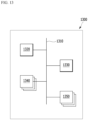
- FIG. 13 is a diagram illustrating a display device that includes one or more visible light sensor embedded OLED display panels according to some example embodiments.
- display device 1300 includes a bus 1310, a processor 1320, a memory 1330, and one or more OLED display panels 1340. As shown, in some example embodiments, the display device 1300 may further include one or more additional devices 1350.
- the processor 1320, a memory 1330, and one or more OLED display panels 1340 (and where present, the one or more additional devices 1350) may communicate with one another through the bus 1310.
- the one or more OLED display panels 1340 may each be any of the visible light sensor embedded OLED display panels included in any of the example embodiments.
- the processor 1320 may include one or more instances of processing circuitry such as hardware including logic circuits; a hardware/software combination such as a processor executing software; or a combination thereof.
- the processing circuitry more specifically may include, but is not limited to, a central processing unit (CPU), an arithmetic logic unit (ALU), a digital signal processor, a microcomputer, a field programmable gate array (FPGA), a System-on-Chip (SoC), a programmable logic unit, a microprocessor, application-specific integrated circuit (ASIC), etc.
- CPU central processing unit
- ALU arithmetic logic unit
- FPGA field programmable gate array
- SoC System-on-Chip
- ASIC application-specific integrated circuit
- the processing circuitry may include a non-transitory computer readable storage device, for example a solid state drive (SSD), storing a program of instructions, and a processor configured to execute the program of instructions to implement the functionality of the processor 1320 and/or one or more OLED display panels 1340.
- SSD solid state drive
- the processing circuitry may include a non-transitory computer readable storage device, for example a solid state drive (SSD), storing a program of instructions, and a processor configured to execute the program of instructions to implement the functionality of the processor 1320 and/or one or more OLED display panels 1340.
- SSD solid state drive
- the processor 1320 may control display operations of the one or more OLED display panels 1340 to display one or more images and/or may control biometric recognition operations implemented based at least in part upon at least one or more light sensors embedded in one or more OLED display panels 1340.
- the one or more additional devices 1350 may include one or more communication interfaces (e.g., wireless communication interface, wired interface), user interfaces (e.g., keypad, mouse, button, etc.), power supply and/or power supply interface, any combination thereof, or the like.
- communication interfaces e.g., wireless communication interface, wired interface
- user interfaces e.g., keypad, mouse, button, etc.
- power supply and/or power supply interface any combination thereof, or the like.
- the memory 1330 may store a program of instructions and the processor 1320 may execute the stored program of instructions to implement functionality associated with the display device 1300 and/or one or more OLED display panels 1340, including performing one or more biometric recognition operations.
- the units and/or modules described herein may be implemented using hardware components and software components.
- the hardware components may include microphones, amplifiers, band-pass filters, audio to digital convertors, and processing devices.
- a processing device may be implemented using one or more hardware device configured to carry out and/or execute program code by performing arithmetical, logical, and input/output operations.
- the processing device(s) may include a processor, a controller and an arithmetic logic unit, a digital signal processor, a microcomputer, a field programmable array, a programmable logic unit, a microprocessor or any other device capable of responding to and executing instructions in a defined manner.
- the processing device may run an operating system (OS) and one or more software applications that run on the OS.
- OS operating system
- the processing device also may access, store, manipulate, process, and create data in response to execution of the software.
- a processing device may include multiple processing elements and multiple types of processing elements.
- a processing device may include multiple processors or a processor and a controller.
- different processing configurations are possible, such a parallel processors.
- the software may include a computer program, a piece of code, an instruction, or some combination thereof, to independently or collectively instruct and/or configure the processing device to operate as desired, thereby transforming the processing device into a special purpose processor.
- Software and data may be embodied permanently or temporarily in any type of machine, component, physical or virtual equipment, computer storage medium or device, or in a propagated signal wave capable of providing instructions or data to or being interpreted by the processing device.
- the software also may be distributed over network coupled computer systems so that the software is stored and executed in a distributed fashion.
- the software and data may be stored by one or more non-transitory computer readable recording mediums.
- the methods according to the above-described example embodiments may be recorded in non-transitory computer-readable media including program instructions to implement various operations of the above-described example embodiments.
- the media may also include, alone or in combination with the program instructions, data files, data structures, and the like.
- the program instructions recorded on the media may be those specially designed and constructed for the purposes of example embodiments, or they may be of the kind well-known and available to those having skill in the computer software arts.
- non-transitory computer-readable media examples include magnetic media such as hard disks, floppy disks, and magnetic tape; optical media such as CD-ROM discs, DVDs, and/or Blue-ray discs; magneto-optical media such as optical discs; and hardware devices that are specially configured to store and perform program instructions, such as read-only memory (ROM), random access memory (RAM), flash memory (e.g., USB flash drives, memory cards, memory sticks, etc.), and the like.
- program instructions include both machine code, such as produced by a compiler, and files containing higher level code that may be executed by the computer using an interpreter.
- the above-described devices may be configured to act as one or more software modules in order to perform the operations of the above-described example embodiments, or vice versa.
Landscapes
- Engineering & Computer Science (AREA)
- Theoretical Computer Science (AREA)
- Physics & Mathematics (AREA)
- General Physics & Mathematics (AREA)
- Inorganic Chemistry (AREA)
- Chemical & Material Sciences (AREA)
- Multimedia (AREA)
- General Engineering & Computer Science (AREA)
- Sustainable Development (AREA)
- Life Sciences & Earth Sciences (AREA)
- Human Computer Interaction (AREA)
- Computer Security & Cryptography (AREA)
- Microelectronics & Electronic Packaging (AREA)
- Computer Hardware Design (AREA)
- Software Systems (AREA)
- Electroluminescent Light Sources (AREA)
- Devices For Indicating Variable Information By Combining Individual Elements (AREA)
- Measurement Of The Respiration, Hearing Ability, Form, And Blood Characteristics Of Living Organisms (AREA)
- Photo Coupler, Interrupter, Optical-To-Optical Conversion Devices (AREA)
- Optics & Photonics (AREA)
Applications Claiming Priority (1)
| Application Number | Priority Date | Filing Date | Title |
|---|---|---|---|
| KR20180120055 | 2018-10-08 |
Publications (2)
| Publication Number | Publication Date |
|---|---|
| EP3637472A1 EP3637472A1 (en) | 2020-04-15 |
| EP3637472B1 true EP3637472B1 (en) | 2025-07-02 |
Family
ID=68084678
Family Applications (1)
| Application Number | Title | Priority Date | Filing Date |
|---|---|---|---|
| EP19200233.5A Active EP3637472B1 (en) | 2018-10-08 | 2019-09-27 | Organic light emitting diode display panels and display devices including the same |
Country Status (5)
| Country | Link |
|---|---|
| US (2) | US10978523B2 (ko) |
| EP (1) | EP3637472B1 (ko) |
| JP (1) | JP2020092080A (ko) |
| KR (1) | KR102876928B1 (ko) |
| CN (1) | CN111009556B (ko) |
Families Citing this family (70)
| Publication number | Priority date | Publication date | Assignee | Title |
|---|---|---|---|---|
| KR102566717B1 (ko) * | 2016-12-12 | 2023-08-14 | 삼성전자 주식회사 | 생체 센서를 구비한 전자 장치 |
| US20220052128A1 (en) * | 2018-09-10 | 2022-02-17 | Sharp Kabushiki Kaisha | Display device |
| CN109409269A (zh) * | 2018-10-16 | 2019-03-01 | 维沃移动通信有限公司 | 屏幕组件、电子设备及屏幕组件的控制方法 |
| CN109638046B (zh) * | 2018-12-07 | 2020-10-16 | 武汉华星光电半导体显示技术有限公司 | 具有屏下指纹识别的oled显示装置 |
| CN111597865B (zh) * | 2019-02-20 | 2024-07-02 | 华为技术有限公司 | 屏组件及电子设备 |
| US20220285461A1 (en) * | 2019-08-08 | 2022-09-08 | Semiconductor Energy Laboratory Co., Ltd. | Display Device and Electronic Device |
| US11527582B1 (en) | 2019-09-24 | 2022-12-13 | Apple Inc. | Display stack with integrated photodetectors |
| US11611058B2 (en) | 2019-09-24 | 2023-03-21 | Apple Inc. | Devices and systems for under display image sensor |
| CN110867468A (zh) * | 2019-10-30 | 2020-03-06 | 深圳市华星光电半导体显示技术有限公司 | 一种显示面板及其制作方法 |
| CN210515327U (zh) * | 2019-11-29 | 2020-05-12 | 京东方科技集团股份有限公司 | 一种显示装置 |
| WO2021140404A1 (ja) * | 2020-01-10 | 2021-07-15 | 株式会社半導体エネルギー研究所 | 電子機器、及びプログラム |
| US11475699B2 (en) * | 2020-01-22 | 2022-10-18 | Asti Global Inc., Taiwan | Display module and image display thereof |
| JP2023068211A (ja) * | 2020-03-30 | 2023-05-17 | ソニーセミコンダクタソリューションズ株式会社 | 電子機器 |
| TWI723855B (zh) * | 2020-04-28 | 2021-04-01 | 友達光電股份有限公司 | 發光二極體顯示裝置及其製造方法 |
| CN111540775B (zh) * | 2020-05-11 | 2023-07-18 | 京东方科技集团股份有限公司 | 显示基板及其制备方法和亮度补偿方法、显示装置 |
| CN111829573B (zh) * | 2020-06-01 | 2022-06-24 | 惠州市德赛西威汽车电子股份有限公司 | 一种光感传感器耐久测试设备及方法 |
| TWI910180B (zh) * | 2020-06-26 | 2026-01-01 | 日商半導體能源研究所股份有限公司 | 顯示裝置及電子裝置 |
| CN111681551B (zh) * | 2020-06-28 | 2021-07-06 | 武汉华星光电技术有限公司 | 显示模组以及电子设备 |
| US12536829B2 (en) * | 2020-06-30 | 2026-01-27 | Sharp Kabushiki Kaisha | Electromagnetic wave sensor device and display device |
| KR102928670B1 (ko) * | 2020-07-23 | 2026-02-23 | 삼성디스플레이 주식회사 | 표시 장치 |
| CN112018157B (zh) * | 2020-08-05 | 2022-05-31 | 武汉华星光电技术有限公司 | 显示装置 |
| CN111785766A (zh) * | 2020-08-24 | 2020-10-16 | 京东方科技集团股份有限公司 | 显示装置、显示面板及其制备方法 |
| US12170271B2 (en) * | 2020-09-02 | 2024-12-17 | Apple Inc. | Embedded optical sensors in a micro-led display |
| KR20220031402A (ko) * | 2020-09-04 | 2022-03-11 | 삼성전자주식회사 | 전자 장치 |
| WO2022053908A1 (ja) * | 2020-09-11 | 2022-03-17 | 株式会社半導体エネルギー研究所 | 表示装置、表示モジュール、及び電子機器 |
| CN116057607A (zh) * | 2020-09-11 | 2023-05-02 | 株式会社半导体能源研究所 | 显示装置、显示模块及电子设备 |
| KR102899741B1 (ko) * | 2020-11-02 | 2025-12-12 | 엘지디스플레이 주식회사 | 표시장치 |
| CN114594619A (zh) * | 2020-12-04 | 2022-06-07 | 中兴通讯股份有限公司 | 偏光片结构、终端设备及终端设备进光量控制方法 |
| TWI765457B (zh) * | 2020-12-09 | 2022-05-21 | 友達光電股份有限公司 | 顯示裝置及掃描影像的方法 |
| TWI757036B (zh) * | 2021-01-06 | 2022-03-01 | 友達光電股份有限公司 | 觸控顯示面板 |
| KR20220107439A (ko) * | 2021-01-25 | 2022-08-02 | 삼성전자주식회사 | 생체정보 추정 장치 및 방법 |
| CN116724349A (zh) * | 2021-01-28 | 2023-09-08 | 株式会社半导体能源研究所 | 显示装置 |
| WO2022162493A1 (ja) * | 2021-01-28 | 2022-08-04 | 株式会社半導体エネルギー研究所 | 表示装置、表示モジュール、電子機器、及び、表示装置の作製方法 |
| KR20230142526A (ko) * | 2021-02-02 | 2023-10-11 | 가부시키가이샤 한도오따이 에네루기 켄큐쇼 | 표시 장치, 표시 모듈, 및 전자 기기 |
| US20240130163A1 (en) * | 2021-02-19 | 2024-04-18 | Semiconductor Energy Laboratory Co., Ltd. | Display apparatus, manufacturing method of the display apparatus, display module, and electronic device |
| US11839133B2 (en) | 2021-03-12 | 2023-12-05 | Apple Inc. | Organic photodetectors for in-cell optical sensing |
| EP4102572A3 (en) * | 2021-04-23 | 2023-04-05 | Samsung Electronics Co., Ltd. | Sensor-embedded display panel and electronic device |
| CN113161407B (zh) * | 2021-04-28 | 2024-04-23 | 京东方科技集团股份有限公司 | 显示基板、其驱动方法及显示装置 |
| KR20220161770A (ko) | 2021-05-31 | 2022-12-07 | 삼성전자주식회사 | 센서 내장형 표시 패널 및 전자 장치 |
| KR102899003B1 (ko) * | 2021-06-07 | 2025-12-12 | 삼성전자 주식회사 | 광 센서가 포함된 디스플레이를 갖는 전자 장치 |
| EP4322514B1 (en) | 2021-06-07 | 2026-05-06 | Samsung Electronics Co., Ltd. | Electronic apparatus having display including optical sensor |
| KR20230018099A (ko) | 2021-07-29 | 2023-02-07 | 삼성전자주식회사 | 화합물, 센서, 센서 내장형 표시 패널 및 전자 장치 |
| US12124002B2 (en) | 2021-09-03 | 2024-10-22 | Apple Inc. | Beam deflector metasurface |
| CN113780179B (zh) * | 2021-09-13 | 2023-08-29 | 武汉华星光电半导体显示技术有限公司 | 柔性显示模组及显示终端 |
| US20230087411A1 (en) * | 2021-09-23 | 2023-03-23 | Apple Inc. | Electronic Devices Having Quantum Film Infrared Sensors |
| US12197665B2 (en) | 2021-09-24 | 2025-01-14 | Apple Inc. | Touch and light sensing using integrated micro circuitry |
| US20240407225A1 (en) * | 2021-09-30 | 2024-12-05 | Semiconductor Energy Laboratory Co., Ltd. | Display apparatus |
| KR20230048213A (ko) * | 2021-10-01 | 2023-04-11 | 삼성디스플레이 주식회사 | 표시 장치 |
| KR102908920B1 (ko) | 2021-10-28 | 2026-01-09 | 삼성디스플레이 주식회사 | 전자 장치 |
| KR20230085421A (ko) * | 2021-12-07 | 2023-06-14 | 엘지디스플레이 주식회사 | 표시장치 |
| US20250040288A1 (en) * | 2021-12-08 | 2025-01-30 | Lumileds Llc | Monolithic Optical Transformer |
| KR20230091215A (ko) | 2021-12-15 | 2023-06-23 | 삼성디스플레이 주식회사 | 전자 장치 및 전자 장치의 구동 방법 |
| CN114384994B (zh) * | 2021-12-31 | 2023-11-28 | 厦门天马微电子有限公司 | 一种显示装置及其驱动方法和电子设备 |
| WO2023125329A1 (zh) * | 2021-12-31 | 2023-07-06 | 北京与光科技有限公司 | 活体指纹识别系统及其活体识别方法 |
| JP7829836B2 (ja) * | 2022-01-18 | 2026-03-16 | 日産自動車株式会社 | 測距センサ |
| CN114795162B (zh) * | 2022-04-18 | 2025-05-23 | 北京京东方光电科技有限公司 | 指静脉传感器及电子设备 |
| US12433088B2 (en) | 2022-05-31 | 2025-09-30 | Samsung Electronics Co., Ltd. | Sensor embedded display panel and electronic device |
| KR20240007971A (ko) * | 2022-07-08 | 2024-01-18 | 삼성디스플레이 주식회사 | 표시 장치 |
| CN119768854A (zh) * | 2022-07-18 | 2025-04-04 | Oti公司 | 在具有均匀(子)像素孔布局的发射区域之间具有透射区域的光电子器件 |
| KR20240018725A (ko) * | 2022-08-02 | 2024-02-14 | 삼성디스플레이 주식회사 | 표시 장치 |
| KR20240058658A (ko) | 2022-10-26 | 2024-05-03 | 삼성전자주식회사 | 센서, 센서 어레이, 표시 패널 및 전자 장치 |
| KR20240078472A (ko) * | 2022-11-24 | 2024-06-04 | 삼성전자주식회사 | 센서 내장형 표시 패널 및 전자 장치 |
| KR20240118212A (ko) * | 2023-01-25 | 2024-08-05 | 삼성디스플레이 주식회사 | 표시 장치 |
| KR20240142799A (ko) * | 2023-03-22 | 2024-10-02 | 삼성전자주식회사 | 표시 패널 및 전자 장치 |
| KR20240151902A (ko) * | 2023-04-11 | 2024-10-18 | 삼성디스플레이 주식회사 | 표시 장치 |
| US20240363088A1 (en) * | 2023-04-26 | 2024-10-31 | Apple Inc. | Electronic Device With Display Light Sensor |
| CN119012834A (zh) * | 2023-05-17 | 2024-11-22 | 京东方科技集团股份有限公司 | 显示面板及其制备方法、驱动方法、显示装置 |
| KR20250050983A (ko) * | 2023-10-05 | 2025-04-16 | 삼성디스플레이 주식회사 | 표시 장치 |
| WO2025204186A1 (ja) * | 2024-03-29 | 2025-10-02 | ソニーグループ株式会社 | 発光装置および画像表示装置 |
| KR20250147939A (ko) * | 2024-04-02 | 2025-10-14 | 삼성디스플레이 주식회사 | 조도 센서 및 이를 포함하는 표시 장치 |
Citations (4)
| Publication number | Priority date | Publication date | Assignee | Title |
|---|---|---|---|---|
| US6747290B2 (en) * | 2000-12-12 | 2004-06-08 | Semiconductor Energy Laboratory Co., Ltd. | Information device |
| US20130075761A1 (en) * | 2011-09-26 | 2013-03-28 | Masahiko Akiyama | Photoelectric conversion device and manufacturing method thereof |
| US20170255811A1 (en) * | 2016-03-07 | 2017-09-07 | Microsoft Technology Licensing, Llc | Image sensing with a display |
| WO2018130110A1 (zh) * | 2017-01-10 | 2018-07-19 | 京东方科技集团股份有限公司 | 触控基板及显示装置 |
Family Cites Families (27)
| Publication number | Priority date | Publication date | Assignee | Title |
|---|---|---|---|---|
| KR20000013995A (ko) | 1998-08-10 | 2000-03-06 | 최환수 | 지문영상 검출소자 및 그 장치 |
| JP2004016407A (ja) | 2002-06-14 | 2004-01-22 | Canon Inc | 画像検出装置および携帯機器 |
| JP2008191611A (ja) * | 2007-02-08 | 2008-08-21 | Sony Corp | 有機el表示装置、有機el表示装置の制御方法および電子機器 |
| JP4501947B2 (ja) * | 2007-02-26 | 2010-07-14 | エプソンイメージングデバイス株式会社 | 電気光学装置、表示装置およびこれを備える電子機器 |
| CA2749607C (en) | 2009-01-14 | 2018-03-13 | Perceptive Pixel Inc. | Touch-sensitive display |
| KR101113538B1 (ko) * | 2009-11-03 | 2012-03-02 | 삼성모바일디스플레이주식회사 | 터치 스크린 내장형 평판표시장치 및 그 구동방법 |
| US9666635B2 (en) | 2010-02-19 | 2017-05-30 | Synaptics Incorporated | Fingerprint sensing circuit |
| KR20130119614A (ko) * | 2012-04-24 | 2013-11-01 | 삼성디스플레이 주식회사 | 센싱 장치 및 이미지 센싱 방법 |
| KR101418760B1 (ko) | 2013-01-28 | 2014-07-11 | 실리콘 디스플레이 (주) | 투명 지문인식 센서 어레이 |
| US9277894B2 (en) * | 2014-02-13 | 2016-03-08 | General Electric Company | Method and system for integrated patient table digital X-ray dosimeter |
| US9836165B2 (en) | 2014-05-16 | 2017-12-05 | Apple Inc. | Integrated silicon-OLED display and touch sensor panel |
| KR101758047B1 (ko) | 2014-09-04 | 2017-07-17 | 크루셜텍 (주) | 이미지 센싱이 가능한 표시 장치 |
| KR20160056759A (ko) | 2014-11-12 | 2016-05-20 | 크루셜텍 (주) | 이미지 스캔이 가능한 플렉서블 디스플레이 장치 및 이의 구동 방법 |
| US9891746B2 (en) | 2014-11-12 | 2018-02-13 | Crucialtec Co., Ltd. | Display apparatus capable of image scanning and driving method thereof |
| US9679182B2 (en) | 2014-11-12 | 2017-06-13 | Crucialtec Co., Ltd. | Display apparatus capable of image scanning and driving method thereof |
| KR20170000103A (ko) | 2015-06-23 | 2017-01-02 | 주식회사 엔에프디 | 지문 인식 장치 |
| KR20170049731A (ko) | 2015-10-28 | 2017-05-11 | 크루셜텍 (주) | 지문 이미지 센싱 장치 및 이를 포함하는 표시 장치 |
| CN108369724A (zh) * | 2015-12-08 | 2018-08-03 | 柯尼卡美能达株式会社 | 光学式指纹认证装置 |
| WO2017126153A1 (ja) * | 2016-01-22 | 2017-07-27 | コニカミノルタ株式会社 | 光学式指紋認証装置 |
| WO2017188715A2 (ko) | 2016-04-28 | 2017-11-02 | 크루셜텍 (주) | 언더글라스 적용이 가능한 발광 지문 인식 패널 및 이를 포함하는 지문 인식 디스플레이 장치 |
| CN107918756A (zh) * | 2016-10-11 | 2018-04-17 | 群创光电股份有限公司 | 指纹感测装置以及显示器 |
| CN108182872B (zh) * | 2016-12-08 | 2021-01-26 | 群创光电股份有限公司 | 具有光感测单元的显示装置 |
| KR102566717B1 (ko) * | 2016-12-12 | 2023-08-14 | 삼성전자 주식회사 | 생체 센서를 구비한 전자 장치 |
| EP3425670B1 (en) | 2017-07-04 | 2024-11-27 | Samsung Electronics Co., Ltd. | Near-infrared light organic sensors, embedded organic light emitting diode panels, and display devices including the same |
| CN107451576B (zh) | 2017-08-09 | 2020-05-08 | 上海天马微电子有限公司 | 一种阵列基板及其制备方法、显示面板和显示装置 |
| CN107680988B (zh) * | 2017-09-15 | 2020-03-13 | 上海天马微电子有限公司 | 一种显示面板及电子设备 |
| CN107609538B (zh) | 2017-10-12 | 2020-08-04 | 京东方科技集团股份有限公司 | 一种指纹识别装置及指纹识别方法、触控显示装置 |
-
2019
- 2019-09-27 EP EP19200233.5A patent/EP3637472B1/en active Active
- 2019-09-30 CN CN201910938569.5A patent/CN111009556B/zh active Active
- 2019-10-01 KR KR1020190121682A patent/KR102876928B1/ko active Active
- 2019-10-02 US US16/590,886 patent/US10978523B2/en active Active
- 2019-10-08 JP JP2019185002A patent/JP2020092080A/ja active Pending
-
2021
- 2021-04-12 US US17/227,845 patent/US11716892B2/en active Active
Patent Citations (4)
| Publication number | Priority date | Publication date | Assignee | Title |
|---|---|---|---|---|
| US6747290B2 (en) * | 2000-12-12 | 2004-06-08 | Semiconductor Energy Laboratory Co., Ltd. | Information device |
| US20130075761A1 (en) * | 2011-09-26 | 2013-03-28 | Masahiko Akiyama | Photoelectric conversion device and manufacturing method thereof |
| US20170255811A1 (en) * | 2016-03-07 | 2017-09-07 | Microsoft Technology Licensing, Llc | Image sensing with a display |
| WO2018130110A1 (zh) * | 2017-01-10 | 2018-07-19 | 京东方科技集团股份有限公司 | 触控基板及显示装置 |
Also Published As
| Publication number | Publication date |
|---|---|
| CN111009556B (zh) | 2024-01-26 |
| JP2020092080A (ja) | 2020-06-11 |
| KR102876928B1 (ko) | 2025-10-28 |
| US20200111851A1 (en) | 2020-04-09 |
| CN111009556A (zh) | 2020-04-14 |
| US20210257420A1 (en) | 2021-08-19 |
| US10978523B2 (en) | 2021-04-13 |
| EP3637472A1 (en) | 2020-04-15 |
| KR20200040196A (ko) | 2020-04-17 |
| US11716892B2 (en) | 2023-08-01 |
Similar Documents
| Publication | Publication Date | Title |
|---|---|---|
| EP3637472B1 (en) | Organic light emitting diode display panels and display devices including the same | |
| JP7245611B2 (ja) | 近赤外線有機光センサが組み込まれた有機発光ダイオードパネル及びこれを含む表示装置 | |
| CN107066162B (zh) | 一种显示面板及显示装置 | |
| US11482051B2 (en) | Display apparatus and pattern identification method thereof | |
| CN108183110B (zh) | 显示面板和显示装置 | |
| CN108604296B (zh) | 发光指纹识别面板及包括其的指纹识别显示装置 | |
| US9836165B2 (en) | Integrated silicon-OLED display and touch sensor panel | |
| CN110753999A (zh) | 用于使用基于点的照亮的光学感测的系统和方法 | |
| CN109886140B (zh) | 显示面板及其制作方法和显示装置 | |
| KR20220031402A (ko) | 전자 장치 | |
| CN113901857B (zh) | 纹路识别装置以及电子装置 | |
| US11625941B2 (en) | Fingerprint sensors and fingerprint sensor arrays and devices | |
| US20240427444A1 (en) | Touch panel and display device | |
| CN108565279A (zh) | 一种有机发光显示装置和电子设备 | |
| CN110703941A (zh) | 触控结构及其制备方法、触控基板、触控显示装置 | |
| CN113836968A (zh) | 纹路识别装置以及电子装置 | |
| CN113990897A (zh) | 显示面板及包括其的电子设备 | |
| CN116391257A (zh) | 显示装置 | |
| CN111293159B (zh) | 显示基板及显示装置 | |
| US12481397B2 (en) | Electronic device |
Legal Events
| Date | Code | Title | Description |
|---|---|---|---|
| PUAI | Public reference made under article 153(3) epc to a published international application that has entered the european phase |
Free format text: ORIGINAL CODE: 0009012 |
|
| STAA | Information on the status of an ep patent application or granted ep patent |
Free format text: STATUS: THE APPLICATION HAS BEEN PUBLISHED |
|
| STAA | Information on the status of an ep patent application or granted ep patent |
Free format text: STATUS: REQUEST FOR EXAMINATION WAS MADE |
|
| AK | Designated contracting states |
Kind code of ref document: A1 Designated state(s): AL AT BE BG CH CY CZ DE DK EE ES FI FR GB GR HR HU IE IS IT LI LT LU LV MC MK MT NL NO PL PT RO RS SE SI SK SM TR |
|
| AX | Request for extension of the european patent |
Extension state: BA ME |
|
| 17P | Request for examination filed |
Effective date: 20200325 |
|
| RBV | Designated contracting states (corrected) |
Designated state(s): AL AT BE BG CH CY CZ DE DK EE ES FI FR GB GR HR HU IE IS IT LI LT LU LV MC MK MT NL NO PL PT RO RS SE SI SK SM TR |
|
| STAA | Information on the status of an ep patent application or granted ep patent |
Free format text: STATUS: EXAMINATION IS IN PROGRESS |
|
| 17Q | First examination report despatched |
Effective date: 20210211 |
|
| P01 | Opt-out of the competence of the unified patent court (upc) registered |
Effective date: 20230519 |
|
| REG | Reference to a national code |
Ref country code: DE Ref legal event code: R079 Free format text: PREVIOUS MAIN CLASS: H01L0027320000 Ipc: H10K0039320000 Ref country code: DE Ref legal event code: R079 Ref document number: 602019071866 Country of ref document: DE Free format text: PREVIOUS MAIN CLASS: H01L0027320000 Ipc: H10K0039320000 |
|
| GRAP | Despatch of communication of intention to grant a patent |
Free format text: ORIGINAL CODE: EPIDOSNIGR1 |
|
| STAA | Information on the status of an ep patent application or granted ep patent |
Free format text: STATUS: GRANT OF PATENT IS INTENDED |
|
| RIC1 | Information provided on ipc code assigned before grant |
Ipc: G06V 10/143 20220101ALI20250107BHEP Ipc: G06F 21/32 20130101ALI20250107BHEP Ipc: G06V 40/13 20220101ALI20250107BHEP Ipc: H10K 77/00 20230101ALI20250107BHEP Ipc: H10K 59/80 20230101ALI20250107BHEP Ipc: H10K 59/65 20230101ALI20250107BHEP Ipc: H10K 59/12 20230101ALI20250107BHEP Ipc: H10K 59/35 20230101ALI20250107BHEP Ipc: H10K 39/32 20230101AFI20250107BHEP |
|
| INTG | Intention to grant announced |
Effective date: 20250124 |
|
| GRAS | Grant fee paid |
Free format text: ORIGINAL CODE: EPIDOSNIGR3 |
|
| GRAA | (expected) grant |
Free format text: ORIGINAL CODE: 0009210 |
|
| STAA | Information on the status of an ep patent application or granted ep patent |
Free format text: STATUS: THE PATENT HAS BEEN GRANTED |
|
| AK | Designated contracting states |
Kind code of ref document: B1 Designated state(s): AL AT BE BG CH CY CZ DE DK EE ES FI FR GB GR HR HU IE IS IT LI LT LU LV MC MK MT NL NO PL PT RO RS SE SI SK SM TR |
|
| REG | Reference to a national code |
Ref country code: GB Ref legal event code: FG4D |
|
| REG | Reference to a national code |
Ref country code: CH Ref legal event code: EP |
|
| REG | Reference to a national code |
Ref country code: DE Ref legal event code: R096 Ref document number: 602019071866 Country of ref document: DE |
|
| REG | Reference to a national code |
Ref country code: IE Ref legal event code: FG4D |
|
| PGFP | Annual fee paid to national office [announced via postgrant information from national office to epo] |
Ref country code: DE Payment date: 20250813 Year of fee payment: 7 |
|
| PGFP | Annual fee paid to national office [announced via postgrant information from national office to epo] |
Ref country code: GB Payment date: 20250814 Year of fee payment: 7 |
|
| PGFP | Annual fee paid to national office [announced via postgrant information from national office to epo] |
Ref country code: FR Payment date: 20250808 Year of fee payment: 7 |
|
| REG | Reference to a national code |
Ref country code: NL Ref legal event code: MP Effective date: 20250702 |
|
| PG25 | Lapsed in a contracting state [announced via postgrant information from national office to epo] |
Ref country code: PT Free format text: LAPSE BECAUSE OF FAILURE TO SUBMIT A TRANSLATION OF THE DESCRIPTION OR TO PAY THE FEE WITHIN THE PRESCRIBED TIME-LIMIT Effective date: 20251103 |
|
| PG25 | Lapsed in a contracting state [announced via postgrant information from national office to epo] |
Ref country code: NL Free format text: LAPSE BECAUSE OF FAILURE TO SUBMIT A TRANSLATION OF THE DESCRIPTION OR TO PAY THE FEE WITHIN THE PRESCRIBED TIME-LIMIT Effective date: 20250702 |
|
| REG | Reference to a national code |
Ref country code: AT Ref legal event code: MK05 Ref document number: 1810851 Country of ref document: AT Kind code of ref document: T Effective date: 20250702 |
|
| PG25 | Lapsed in a contracting state [announced via postgrant information from national office to epo] |
Ref country code: IS Free format text: LAPSE BECAUSE OF FAILURE TO SUBMIT A TRANSLATION OF THE DESCRIPTION OR TO PAY THE FEE WITHIN THE PRESCRIBED TIME-LIMIT Effective date: 20251102 |
|
| PG25 | Lapsed in a contracting state [announced via postgrant information from national office to epo] |
Ref country code: NO Free format text: LAPSE BECAUSE OF FAILURE TO SUBMIT A TRANSLATION OF THE DESCRIPTION OR TO PAY THE FEE WITHIN THE PRESCRIBED TIME-LIMIT Effective date: 20251002 |
|
| REG | Reference to a national code |
Ref country code: LT Ref legal event code: MG9D |
|
| PG25 | Lapsed in a contracting state [announced via postgrant information from national office to epo] |
Ref country code: AT Free format text: LAPSE BECAUSE OF FAILURE TO SUBMIT A TRANSLATION OF THE DESCRIPTION OR TO PAY THE FEE WITHIN THE PRESCRIBED TIME-LIMIT Effective date: 20250702 |
|
| PG25 | Lapsed in a contracting state [announced via postgrant information from national office to epo] |
Ref country code: FI Free format text: LAPSE BECAUSE OF FAILURE TO SUBMIT A TRANSLATION OF THE DESCRIPTION OR TO PAY THE FEE WITHIN THE PRESCRIBED TIME-LIMIT Effective date: 20250702 |
|
| PG25 | Lapsed in a contracting state [announced via postgrant information from national office to epo] |
Ref country code: HR Free format text: LAPSE BECAUSE OF FAILURE TO SUBMIT A TRANSLATION OF THE DESCRIPTION OR TO PAY THE FEE WITHIN THE PRESCRIBED TIME-LIMIT Effective date: 20250702 |
|
| PG25 | Lapsed in a contracting state [announced via postgrant information from national office to epo] |
Ref country code: GR Free format text: LAPSE BECAUSE OF FAILURE TO SUBMIT A TRANSLATION OF THE DESCRIPTION OR TO PAY THE FEE WITHIN THE PRESCRIBED TIME-LIMIT Effective date: 20251003 |
|
| PG25 | Lapsed in a contracting state [announced via postgrant information from national office to epo] |
Ref country code: CZ Free format text: LAPSE BECAUSE OF FAILURE TO SUBMIT A TRANSLATION OF THE DESCRIPTION OR TO PAY THE FEE WITHIN THE PRESCRIBED TIME-LIMIT Effective date: 20250702 Ref country code: SE Free format text: LAPSE BECAUSE OF FAILURE TO SUBMIT A TRANSLATION OF THE DESCRIPTION OR TO PAY THE FEE WITHIN THE PRESCRIBED TIME-LIMIT Effective date: 20250702 |
|
| PG25 | Lapsed in a contracting state [announced via postgrant information from national office to epo] |
Ref country code: LV Free format text: LAPSE BECAUSE OF FAILURE TO SUBMIT A TRANSLATION OF THE DESCRIPTION OR TO PAY THE FEE WITHIN THE PRESCRIBED TIME-LIMIT Effective date: 20250702 |
|
| PG25 | Lapsed in a contracting state [announced via postgrant information from national office to epo] |
Ref country code: BG Free format text: LAPSE BECAUSE OF FAILURE TO SUBMIT A TRANSLATION OF THE DESCRIPTION OR TO PAY THE FEE WITHIN THE PRESCRIBED TIME-LIMIT Effective date: 20250702 Ref country code: PL Free format text: LAPSE BECAUSE OF FAILURE TO SUBMIT A TRANSLATION OF THE DESCRIPTION OR TO PAY THE FEE WITHIN THE PRESCRIBED TIME-LIMIT Effective date: 20250702 |
|
| PG25 | Lapsed in a contracting state [announced via postgrant information from national office to epo] |
Ref country code: RS Free format text: LAPSE BECAUSE OF FAILURE TO SUBMIT A TRANSLATION OF THE DESCRIPTION OR TO PAY THE FEE WITHIN THE PRESCRIBED TIME-LIMIT Effective date: 20251002 |
|
| PG25 | Lapsed in a contracting state [announced via postgrant information from national office to epo] |
Ref country code: ES Free format text: LAPSE BECAUSE OF FAILURE TO SUBMIT A TRANSLATION OF THE DESCRIPTION OR TO PAY THE FEE WITHIN THE PRESCRIBED TIME-LIMIT Effective date: 20250702 |
|
| PG25 | Lapsed in a contracting state [announced via postgrant information from national office to epo] |
Ref country code: RO Free format text: LAPSE BECAUSE OF FAILURE TO SUBMIT A TRANSLATION OF THE DESCRIPTION OR TO PAY THE FEE WITHIN THE PRESCRIBED TIME-LIMIT Effective date: 20250702 |
|
| PG25 | Lapsed in a contracting state [announced via postgrant information from national office to epo] |
Ref country code: SM Free format text: LAPSE BECAUSE OF FAILURE TO SUBMIT A TRANSLATION OF THE DESCRIPTION OR TO PAY THE FEE WITHIN THE PRESCRIBED TIME-LIMIT Effective date: 20250702 |
|
| PG25 | Lapsed in a contracting state [announced via postgrant information from national office to epo] |
Ref country code: DK Free format text: LAPSE BECAUSE OF FAILURE TO SUBMIT A TRANSLATION OF THE DESCRIPTION OR TO PAY THE FEE WITHIN THE PRESCRIBED TIME-LIMIT Effective date: 20250702 |
|
| PG25 | Lapsed in a contracting state [announced via postgrant information from national office to epo] |
Ref country code: IT Free format text: LAPSE BECAUSE OF FAILURE TO SUBMIT A TRANSLATION OF THE DESCRIPTION OR TO PAY THE FEE WITHIN THE PRESCRIBED TIME-LIMIT Effective date: 20250702 |
|
| REG | Reference to a national code |
Ref country code: CH Ref legal event code: H13 Free format text: ST27 STATUS EVENT CODE: U-0-0-H10-H13 (AS PROVIDED BY THE NATIONAL OFFICE) Effective date: 20260425 |
|
| PG25 | Lapsed in a contracting state [announced via postgrant information from national office to epo] |
Ref country code: SK Free format text: LAPSE BECAUSE OF FAILURE TO SUBMIT A TRANSLATION OF THE DESCRIPTION OR TO PAY THE FEE WITHIN THE PRESCRIBED TIME-LIMIT Effective date: 20250702 Ref country code: EE Free format text: LAPSE BECAUSE OF FAILURE TO SUBMIT A TRANSLATION OF THE DESCRIPTION OR TO PAY THE FEE WITHIN THE PRESCRIBED TIME-LIMIT Effective date: 20250702 |