EP3637619B1 - Traitement et conversion de signaux - Google Patents
Traitement et conversion de signaux Download PDFInfo
- Publication number
- EP3637619B1 EP3637619B1 EP19201272.2A EP19201272A EP3637619B1 EP 3637619 B1 EP3637619 B1 EP 3637619B1 EP 19201272 A EP19201272 A EP 19201272A EP 3637619 B1 EP3637619 B1 EP 3637619B1
- Authority
- EP
- European Patent Office
- Prior art keywords
- dac
- output
- signal
- adc
- digital
- Prior art date
- Legal status (The legal status is an assumption and is not a legal conclusion. Google has not performed a legal analysis and makes no representation as to the accuracy of the status listed.)
- Active
Links
Images




Classifications
-
- H—ELECTRICITY
- H03—ELECTRONIC CIRCUITRY
- H03M—CODING; DECODING; CODE CONVERSION IN GENERAL
- H03M1/00—Analogue/digital conversion; Digital/analogue conversion
- H03M1/10—Calibration or testing
- H03M1/1009—Calibration
- H03M1/1014—Calibration at one point of the transfer characteristic, i.e. by adjusting a single reference value, e.g. bias or gain error
-
- H—ELECTRICITY
- H03—ELECTRONIC CIRCUITRY
- H03M—CODING; DECODING; CODE CONVERSION IN GENERAL
- H03M1/00—Analogue/digital conversion; Digital/analogue conversion
- H03M1/10—Calibration or testing
- H03M1/1009—Calibration
- H03M1/1033—Calibration over the full range of the converter, e.g. for correcting differential non-linearity
- H03M1/1057—Calibration over the full range of the converter, e.g. for correcting differential non-linearity by trimming, i.e. by individually adjusting at least part of the quantisation value generators or stages to their nominal values
- H03M1/1061—Calibration over the full range of the converter, e.g. for correcting differential non-linearity by trimming, i.e. by individually adjusting at least part of the quantisation value generators or stages to their nominal values using digitally programmable trimming circuits
-
- H—ELECTRICITY
- H03—ELECTRONIC CIRCUITRY
- H03M—CODING; DECODING; CODE CONVERSION IN GENERAL
- H03M1/00—Analogue/digital conversion; Digital/analogue conversion
- H03M1/06—Continuously compensating for, or preventing, undesired influence of physical parameters
-
- H—ELECTRICITY
- H03—ELECTRONIC CIRCUITRY
- H03M—CODING; DECODING; CODE CONVERSION IN GENERAL
- H03M1/00—Analogue/digital conversion; Digital/analogue conversion
- H03M1/002—Provisions or arrangements for saving power, e.g. by allowing a sleep mode, using lower supply voltage for downstream stages, using multiple clock domains or by selectively turning on stages when needed
-
- H—ELECTRICITY
- H03—ELECTRONIC CIRCUITRY
- H03M—CODING; DECODING; CODE CONVERSION IN GENERAL
- H03M1/00—Analogue/digital conversion; Digital/analogue conversion
- H03M1/12—Analogue/digital converters
- H03M1/18—Automatic control for modifying the range of signals the converter can handle, e.g. gain ranging
-
- H—ELECTRICITY
- H03—ELECTRONIC CIRCUITRY
- H03M—CODING; DECODING; CODE CONVERSION IN GENERAL
- H03M1/00—Analogue/digital conversion; Digital/analogue conversion
- H03M1/66—Digital/analogue converters
-
- H—ELECTRICITY
- H03—ELECTRONIC CIRCUITRY
- H03M—CODING; DECODING; CODE CONVERSION IN GENERAL
- H03M3/00—Conversion of analogue values to or from differential modulation
- H03M3/30—Delta-sigma modulation
- H03M3/322—Continuously compensating for, or preventing, undesired influence of physical parameters
-
- H—ELECTRICITY
- H03—ELECTRONIC CIRCUITRY
- H03M—CODING; DECODING; CODE CONVERSION IN GENERAL
- H03M3/00—Conversion of analogue values to or from differential modulation
- H03M3/30—Delta-sigma modulation
- H03M3/38—Calibration
- H03M3/386—Calibration over the full range of the converter, e.g. for correcting differential non-linearity
-
- H—ELECTRICITY
- H03—ELECTRONIC CIRCUITRY
- H03M—CODING; DECODING; CODE CONVERSION IN GENERAL
- H03M3/00—Conversion of analogue values to or from differential modulation
- H03M3/30—Delta-sigma modulation
- H03M3/39—Structural details of delta-sigma modulators, e.g. incremental delta-sigma modulators
- H03M3/412—Structural details of delta-sigma modulators, e.g. incremental delta-sigma modulators characterised by the number of quantisers and their type and resolution
- H03M3/422—Structural details of delta-sigma modulators, e.g. incremental delta-sigma modulators characterised by the number of quantisers and their type and resolution having one quantiser only
- H03M3/424—Structural details of delta-sigma modulators, e.g. incremental delta-sigma modulators characterised by the number of quantisers and their type and resolution having one quantiser only the quantiser being a multiple bit one
-
- H—ELECTRICITY
- H03—ELECTRONIC CIRCUITRY
- H03M—CODING; DECODING; CODE CONVERSION IN GENERAL
- H03M3/00—Conversion of analogue values to or from differential modulation
- H03M3/30—Delta-sigma modulation
- H03M3/50—Digital/analogue converters using delta-sigma modulation as an intermediate step
-
- H—ELECTRICITY
- H03—ELECTRONIC CIRCUITRY
- H03M—CODING; DECODING; CODE CONVERSION IN GENERAL
- H03M1/00—Analogue/digital conversion; Digital/analogue conversion
- H03M1/12—Analogue/digital converters
- H03M1/14—Conversion in steps with each step involving the same or a different conversion means and delivering more than one bit
- H03M1/145—Conversion in steps with each step involving the same or a different conversion means and delivering more than one bit the steps being performed sequentially in series-connected stages
- H03M1/146—Conversion in steps with each step involving the same or a different conversion means and delivering more than one bit the steps being performed sequentially in series-connected stages all stages being simultaneous converters
-
- H—ELECTRICITY
- H03—ELECTRONIC CIRCUITRY
- H03M—CODING; DECODING; CODE CONVERSION IN GENERAL
- H03M3/00—Conversion of analogue values to or from differential modulation
- H03M3/30—Delta-sigma modulation
- H03M3/458—Analogue/digital converters using delta-sigma modulation as an intermediate step
Definitions
- aspects of various embodiments are directed to processing signals involving the conversion of analogue signals to digital signals in an analogue-to-digital converter (ADC), such as where a digital to analog converter (DAC) output signal is combined with an analog ADC input signal.
- ADC analogue-to-digital converter
- DAC digital to analog converter
- a multitude of signal processing applications involve the conversion of received analog signals into digital values for processing. Such approaches have been widely implemented for successfully processing signals in many different applications. For such applications, converting and otherwise processing the signals accurately can be challenging, in view of which much effort may be put forth in ensuring that the resulting signals are accurate.
- ADC One type of ADC involves sigma-delta conversion, in which an analog input signal is sampled and quantized into a digital signal.
- the digital signal may be processed through unary DACs, with the resulting analog signal added to the input signal to reduce errors in the quantization.
- errors in the DACs and/or otherwise present challenges to providing an accurate analog feedback signal.
- the present invention concerns an apparatus for error compensation according to claim 1 and a corresponding method for error compensation according to claim 5.
- Various example embodiments are directed to issues such as those addressed above and/or others which may become apparent from the following disclosure concerning the processing of signals, and particularly the conversion of analog signals to digital signals.
- aspects of the present disclosure involve ascertaining mismatches between respective digital-to-analogue convertor (DAC) circuits, and compensating for the mismatches.
- Such an approach may, for example, involve determining mismatch values for respective DACs by correlating usage of individual DAC components with a (compensated) output signal of the ADC (e.g., a multi-bit sigma-delta ADC).
- each DAC circuit may be part of an overall DAC, with each DAC circuit converting a LSB unit or other portion of a digital signal converted by the overall DAC.
- an apparatus for error compensation includes an analog-to-digital converter (ADC) circuit configured and arranged to convert an analog signal into a digital signal, a plurality of digital-to-analog converter (DAC) circuits respectively configured and arranged to convert a portion of the digital signal into an analog signal, and a compensation circuit configured and arranged to correct an output of the ADC circuit.
- the compensation circuit corrects the output by generating, for each DAC circuit, a feedback signal indicative of an incompatibility between an analog output of the DAC circuit, as converted to a digital signal by the ADC circuit, and digital inputs provided to the DAC circuits.
- Respective gains are applied to the digital inputs from each DAC circuit based on the feedback signal for the corresponding DAC circuit, therein providing modified digital inputs.
- the corrected output is then generated based on a combination of the digital signal output from the ADC and the modified digital inputs to the respective DAC circuits.
- ADC analog-to-digital converter
- DAC digital-to-analog converter
- ADC analog-to-digital converter
- DAC digital-to-analog converter
- ADC analog-to-digital converter
- DAC digital-to-analog converter
- a gain is applied to the unit of the digital signal converted by the DAC circuit based on the feedback signal. Errors in the DAC circuit are compensated using the respective bits of the digital signal with the gain applied thereto.
- the apparatus includes a plurality of variable gain circuits respectively configured and arranged to apply a gain to a portion of a signal provided to a digital-to-analog converter (DAC) circuit based on feedback signals for the respective portions of the signal.
- a feedback circuit is configured and arranged to generate the respective feedback signals for each DAC circuit, each feedback signal being based on an output of the DAC circuit for which it is provided and an input signal provided to the DAC circuit.
- An output circuit is configured and arranged to correct the output of the ADC circuit using the respective outputs of the variable gain circuits.
- aspects of the present disclosure are believed to be applicable to a variety of different types of apparatuses, systems and methods involving signal processing, as may be applicable to a multitude of disparate types of communications.
- aspects of the present disclosure have been shown to be beneficial when used in the context of radio communications, such as those utilized in automobiles and other vehicles, and in these and other applications that may employ sigma-delta ADCs.
- signals converted from analog to digital form are processed to provide feedback and related correction to facilitate characterization and correction of mismatch, error or other processing aspects. While not necessarily so limited, various aspects may be appreciated through the following discussion of non-limiting examples which use exemplary contexts.
- Various embodiments are directed to improving signal processing in an ADC such as a delta-sigma ADC.
- An analog signal is sampled and quantized into a digital signal and delta modulated (encoding the voltage or current of the input signal).
- a corresponding signal e.g., the digital signal or a corresponding thermometer code used in generating the digital signal
- a corresponding signal e.g., the digital signal or a corresponding thermometer code used in generating the digital signal
- the resulting analog feedback signal from the DACs is subtracted (delta) to the input analog signal at it is being processed (a sigma operation can be carried out in a loop filter, which may include integrators (sigma)).
- feedback is generated and provided to the signal corresponding to respective outputs of the DACs, which accounts for mismatch across the respective DACs and improves the resulting signal that is subtracted from the input analog signal.
- a DAC may involve respective units (e.g., circuits) therein, with mismatch between the units being estimated and compensated for.
- a 2-bit quantizer can be used, with the 2-bit value being encoded into a 3-bit code that provides an indication of how the DAC-units are configured.
- Various embodiments are directed toward circuitry and related methods involving the conversion of analog signals to digital signals.
- Such embodiments may, for example, involve a sigma-delta (SD) analog to digital converter (ADC).
- An analog loopfilter with transfer "H” may be fed with a signal obtained by subtracting the main analog input signal and a feedback signal generated by a digital to analog converter (DAC).
- the output of the loopfilter may be sampled and quantized at a high sampling rate.
- the quantizer resolution may be generally low, such as 2 binary bits, and the quantizer may produce a multi-bit (e.g., 3-bit) thermometer coded output.
- thermometer code is shuffled by a random control signal (e.g., pseudo-random signal), resulting in a scrambled thermometer code "D [2:0] .”
- D [2:0] a scrambled thermometer code
- the value of the summed thermometer coded bits is equal to the sum of elements at the output of the quantizer.
- the digital representation for Dx is 0's and 1's, in which a binary 0 is represented by -1, while a binary 1 is represented by +1.
- the shuffled data is converted to the analog domain by the DAC, which may include three unit elements (circuits) each having unit element value "u.”
- Such unit elements may, for example, be implemented as a respective DAC circuit that, together, form the bit outputs of the DAC.
- Each unit can be activated as +u or -u, depending on D [2:0] .
- the outputs of the three unit elements are combined before they are subtracted from the input signal.
- Each DAC element may have a certain mismatch compared to their desired value u.
- the mismatches are represented by ⁇ [2:0] .
- the last term is the error caused by static DAC mismatch, which can be corrected for by adding a term with the opposite value.
- the average values may not be same, since Q e may depend on the DAC-element that was chosen.
- Q e 1 + u ⁇ H contains mainly high-frequency content, since it is filtered by the NTF of the modulator.
- Q e 1 + u ⁇ H ⁇ 0 which limits the contribution of Q e ⁇ D x 1 + u ⁇ H to the error signal.
- the last term in the error signal contains DAC element error information, modulated by the data signals D [2:0] and filtered by the STF.
- an apparatus and or method involves an analog-to-digital converter (ADC) circuit configured and arranged to convert an analog signal into a digital signal, and a plurality of digital-to-analog converter (DAC) circuits, each DAC circuit being configured and arranged to convert a portion of a digital signal into an analog signal.
- a compensation circuit is configured and arranged to generate a compensation output by, for the output of each DAC circuit, generating a feedback signal based on an indication of an incompatibility between the analog conversion of the digital signal and a signal corresponding to a combined output of an analog conversion by all of the DAC circuits.
- a gain is applied to a digital signal corresponding to an input to each DAC circuit, based on the feedback signal, and the compensation output is generated based on a digital signal output by the ADC circuit and the modified digital signal (with the gain applied thereto).
- different gains are applied to different ones of the inputs to the DAC circuits, each gain being tailored to the mismatch of the output of the DAC circuit relative to the output of the other DAC circuits.
- the ADC circuit generates quantized bits, which are also used in providing the corrected output.
- the compensation circuit may be implemented in a variety of manners, using a variety of components.
- the DAC input signal is generated by combining the digital inputs to the DACs with the digital output of the ADC to produce the corrected output.
- the respective component is multiplied with the modified digital input for the particular one of the DACs.
- An averaged product of the DACs is generated by combining the product of the multiplying with the product of the multiplying of the other components of the corrected outputs that correspond to other ones of the DACs to provide a combined product, and dividing the combined product by a total number of the DACs.
- the compensation circuit may, for example, include a variable gain amplifier and feedback circuit configured to apply a variable gain to the digital input used for generating the feedback signal for each respective digital input.
- the feedback signal is generated by combining the digital inputs to the DACs with the digital output of the ADC to produce the corrected output. For each respective component of the corrected output that corresponds to a particular one of the DACs, the respective component is multiplied with the modified digital input for the particular one of the DACs.
- the feedback signal may also be generated by subtracting an averaged value corresponding to the digital inputs provided to all of the DACs. The result of the subtracting may further be combined with the feedback signal.
- the feedback signal may also be generated by setting a variable gain for the DAC circuit to compensate for analog conversion of the portion of the digital signal to which the variable gain is being applied.
- the ADC circuit converts the analog signal into the digital 01 signal with quantized bits.
- the DAC circuits convert, for each quantized bit, a corresponding quantized bit into an analog value.
- the compensation circuit generates the feedback signal based on an indication of an incompatibility between the analog conversion of the quantized bit and a combination of quantized bits provided as inputs to the DAC circuits, and applies the gain to each quantized bit provided as inputs to the DAC circuits, based on the feedback signal.
- the corrected output is generated based on the quantized bits that are modified with the respective gains applied thereto.
- the feedback signal may be generated by subtracting, for respective values corresponding to each DAC circuit, an averaged value corresponding to the digital outputs of all of the DACs.
- the feedback signal may also be generated by combining the result of the subtracting with the feedback signal. Further, different gain values may be applied to different ones of the quantized bits provided to the respective DAC circuits, each gain value being tailored to the mismatch of an output of the ADC circuit relative to a corresponding input to the DAC circuits.
- the input signal to the DACs as characterized herein may be generated using a variety of approaches.
- quantized bits provided are generated and randomized as inputs to the plurality of DAC circuits.
- the input signal is generated from and/or based on the output of the ADC.
- FIG. 1 shows an apparatus 100 as may be implemented in accordance with one or more embodiments.
- the apparatus 100 includes a plurality of DAC units (1-N), with two DACs 110 and 120 shown for simplicity.
- Each DAC receives a digital input, as may correspond to an analog signal being processed by an ADC 130.
- the outputs of the respective DACs are combined at ADC 130 and used with an analog input signal to generate a digital output that is used for feedback.
- the digital input to DAC 110 is combined with the output of the ADC at block 112
- the digital input to DAC 120 is combined with the output of the ADC at block 122
- the respective outputs of the combining at blocks 112 and 122 are averaged at block 140 and utilized to generate a feedback signal at each of blocks 114 and 124.
- the respective feedback signals are provided to a combining circuit 130, which applies a gain to the respective digital inputs and combines the inputs with the gain applied thereto with the output of the ADC to provide a corrected output.
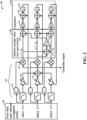
- the DAC output signals are delayed "(z-?)" as shown at block 214, to compensate for delay in the low-pass filter.
- Multipliers including 213) multiply the compensated output (low-pass filtered, corrected Y) with the individual DAC outputs.
- These error indicators contain part of the input signal times STF (transfer function), and on average may be the same for all three indicators.
- the average of the three error signals is generated at 222 and 223 (e.g., added and divided by three), and then subtracted from each error indicator as shown at 221. What is left is (on average) the last term of Equation 13, Equation 14 and Equation 15, which are indicators of the error values.
- Three individual first order control loops with integrator circuitry minimize these error values by adapting the error correction actuators, and provide an output that is fed back to the variable gain circuits, such as at 212, and used to provide the corrected output from adder 215 (e.g., as an ADC input).
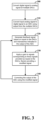
- FIG. 3 is a flow diagram for an approach to converting analog signals to digital signals and related error compensation, as may be implemented in accordance with one or more embodiments.
- a digital signal is converted to an analog signal at multiple DACs.
- An input analog signal is converted signal in an ADC at block 310, using the analog output from the multiple DACs.
- a feedback signal is generated based on input signals provided to the DACs and mismatches indicated in the output of the ADC, which correspond to an analog mismatch in an output of the DACs.
- a gain is applied to signals corresponding to those provided as inputs to the DACs at block 330.
- the output of the ADC is corrected using the modified signal. This output may, for example, be provided for use at block 320, as shown via the arrow in the figure.
- FIG. 4 shows another apparatus 400, for compensating for errors in an ADC.
- the apparatus 400 includes a 2-bit (4-level) DAC 410 that is steered with a 3-bits thermometer code D[2:0] provided to a random selector circuit 420, such as by using a pseudorandom binary sequence (PRBS). Static DAC element errors are indicated by ⁇ p/n0 [2:0].
- the D[2:0] thermometer code may be generated internally or provided as an input from an external source.
- the levels -1*e and +1*e can be made in three ways, based on random selection, resulting in D*[2:0].
- the output of the DAC is combined with an analog input signal and provided to an analog transfer function circuit 430, which may be partly linear or non-linear, and includes an ADC circuit.
- the digital output of the analog transfer function circuit is provided along with the D*[2:0] output of the random selector circuit 420 as inputs for a DAC element estimation and correction circuit 440, which may operate as noted above to provide correction relative to respective values generated in the DAC 410.
- Figure 5 shows a DAC element estimation and correction circuit 500, in accordance with another example embodiment.
- Individual bits D*[2:0] are multiplied with 1 +/- a correction factor, where the correction factors may compensate for ⁇ p/n0 [2:0] errors.
- the corrected values are combined with an input 501 generated by an analog to digital conversion circuit, using a digital combining function/circuit 520.
- the circuit 500 may be implemented for circuit 440 in Figure 4 , with the input D*[2:0] provided by random selection circuit 420 and the input 501 provided by the analog transfer function circuit 430.
- the output of the combining function Y cor is the corrected output and may be used for further processing.
- the outputs of the correlators 531, 532 and 533 provide a measure of how one single DAC element influences a combined output signal. There may be a strong correlation, since the corrected output Y cor is (partly) constructed from D*[2:0]. This correlation may be (on average) common for each correlator output, since the DAC element selection is pseudo random. This common correlation can be removed by subtracting the average output value from each correlator output, with the average output value being generated at 550 and 552 and subtraction respectively carried out for correlations 531, 532 and 533 at 561, 562 and 563. The output of the correlators 531, 532 and 533 (with common correlation subtracted) are fed to integrators with a small integrator gain.
- the integrator outputs are used to steer the correction factors which multiply with D*[2:0].
- the correction values should be such that all correlator outputs are 'balanced' on average, so there is on average no difference between the correlator outputs.
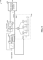
- Figure 6 shows another apparatus 600 for correcting ADC errors, in accordance with another example embodiment.
- the apparatus 600 is similar to apparatus 400 of Figure 4 , with a DAC 610, random selector circuit 620, an analog transfer function circuit 630, and a DAC element estimation and correction circuit 640.
- the analog transfer function circuit 630 includes summations node, where the DAC signal is subtracted from the input signal, followed by an analog loop filter, the output of which is quantized.
- the quantizer has a relatively low resolution. The resolution for a certain frequency band can be increased by an oversampled quantizer clock and a filter transfer of the loop filter. Any error in the feedback will result in a 1-on-1 error on the digital output. In this sigma-delta case, D*[2:0] can be used as the actual digital output signal (uncompensated).
- Figure 7 shows a DAC element estimation and correction circuit 700, in accordance with another example embodiment.
- the circuit 700 may, for example, be implemented for a sigma-delta case such as via circuit 640 in Figure 6 , and in a manner similar to that shown and described with Figure 5 (with similarly numbered componentry). Corrected values are combined with an input 701 generated by an analog to digital conversion circuit, using a digital combining function/circuit 720.
- the circuit 700 further includes optional filter circuit 730 and delay circuit 740, with the filter circuit filtering the output Y cor which is correlated with the individual D*[2:0] bits using multipliers 731, 732 and 733.
- the average output value from each correlator output is generated at 750/752 and subtracted respectively from the output of correlators 731, 732 and 733 at 761, 762 and 763, and provided to integrators 770.
- the integrator outputs are used to steer the correction factors which multiply with D*[2:0].
- both inputs to the digital combining function/circuit 720 are D*[2:0], utilizing the compensated output and ignoring input 701.
- the compensated signal is filtered in such an instance, due to quantization noise.
- the Band-pass or low-pass filter filters the quantization noise out.
- strong signals are filtered, mitigating reductions in convergence accuracy of the error estimation system that may occur due to strong signals. This approach may improve estimation accuracy, and with that the convergence speed.
- Figure 8 shows another apparatus 800 for correcting ADC errors, in accordance with another example embodiment.
- the apparatus 800 is also similar to apparatus 400 of Figure 4 , with a DAC 810, random selector circuit 820, analog transfer function circuit (with an ADC) 830, and a DAC element estimation and correction circuit 840.
- An analog input signal is quantized to the digital domain in two steps, first via coarse digitization at block 821 (e.g., into 4 levels), and via fine digitization at analog transfer function circuit 830.
- a resulting digital code is subtracted from the input signal via DAC 810 and a subtractor 831, and is quantized further with a fine ADC 832.
- An output code is constructed by adding the coarse ADC code and fine ADC code, within the DAC element estimation and correction circuit 840. In some implementations, the linearity of the fine ADC is relaxed, since the input signal is small (despite being visible in the resulting output code).
- Figure 9 shows another DAC element estimation and correction circuit 900, in accordance with another example embodiment.
- the circuit 900 may, for example, be implemented as circuit 840 in Figure 8 , and in a manner similar to that shown and described with Figure 5 and with similarly numbered componentry.
- Digital combining function/circuit 920 combines input 901 with corrected input D[2:0], multipliers 931, 932 and 933 correlate the output Y cor with the inputs.
- the correlated outputs are averaged via averaging circuitry 950/952, with the average being subtracted from the correlated outputs by subtracting circuitry 961, 962 and 963, the output of which is provided to integrators 970 to provide respective feedback signals for compensating each respective input component as shown.
- the coarse codes can be calibrated with variable gains before adding the coarse code with the fine code.
- circuits or circuitry which may be illustrated as or using terms such as blocks, modules, device, system, unit, controller, converter, integrator, and/or other circuit-type depictions (e.g., reference numerals 112, 114, 122, 124, 130 and 140 of Figure 1 , depict a block/module as described herein).
- circuits or circuitry are used together with other elements to exemplify how certain embodiments may be carried out in the form or structures, steps, functions, operations, activities, etc.
- one or more modules are discrete logic circuits or programmable logic circuits configured and arranged for implementing these operations/activities, as may be carried out in the approaches shown in Figures 1-9 .
- a programmable circuit is one or more computer circuits, including memory circuitry for storing and accessing a program to be executed as a set (or sets) of instructions (and/or to be used as configuration data to define how the programmable circuit is to perform), and an algorithm or process as described in connection with error estimation herein, such as shown in and described in connection with Figure 3 , is used by the programmable circuit to perform the related steps, functions, operations, activities, etc.
- the instructions (and/or configuration data) can be configured for implementation in logic circuitry, with the instructions (whether characterized in the form of object code, firmware or software) stored in and accessible from a memory (circuit).
- a memory accessible from a memory (circuit).
- the adjectives "first” and “second” are not used to connote any description of the structure or to provide any substantive meaning; rather, such adjectives are merely used for English-language antecedence to differentiate one such similarly-named structure from another similarly-named structure (e.g., "first circuit configured to combine " is interpreted as “circuit configured to combine").
Landscapes
- Engineering & Computer Science (AREA)
- Theoretical Computer Science (AREA)
- Physics & Mathematics (AREA)
- Nonlinear Science (AREA)
- Analogue/Digital Conversion (AREA)
- Compression, Expansion, Code Conversion, And Decoders (AREA)
Claims (5)
- Appareil de compensation d'erreur (100), l'appareil (100) comprenant :un circuit convertisseur analogique-numérique, CAN, (130) configuré et disposé de manière à convertir un signal analogique appliqué à l'entrée du CAN en un signal numérique (501 ; 701 ; 901) au niveau de la sortie du CAN ;une pluralité de circuits convertisseurs numérique-analogique, CNA, (110, 120), chaque CNA (110, 120) étant configuré et disposé pour convertir une partie respective d'un code de thermomètre brouillé (D*[2:0]) qui est générée à la suite du brassage d'un code de thermomètre correspondant au signal (501, 701, 901) à la sortie du CAN (130) et qui est appliquée à l'entrée numérique du CNA (110, 120) en un signal analogique respectif au niveau de la sortie du CNA (110, 120) ; etun circuit de compensation (200 ; 500 ; 700 ; 900) configuré et disposé de manière à corriger le signal numérique (501; 701 ; 901) à la sortie du CAN (130) par :pour chaque CNA (110, 120), génération d'un signal de rétroaction respectif indicatif d'une non-concordance entre le signal analogique respectif au niveau de la sortie du CNA (110, 120), tel que converti en un signal numérique correspondant par le CAN (130) et la partie respective du code de thermomètre brouillé (D*[2:0]) fournie au CNA (110, 120) ;pour chaque CNA (110, 120), application d'un gain respectif à l'entrée numérique du CNA (110, 120) en fonction du signal de rétroaction respectif pour le CNA (110, 120), en fournissant ainsi un signal numérique modifié respectif ;
etgénération d'une sortie corrigée (Ycor) en fonction d'une combinaison du signal numérique (510 ; 701 ; 901) au niveau de la sortie du CAN (130) et des signaux numériques modifiés respectifs de chaque CNA (110, 120) ; (110, 120) ;la génération du signal de rétroaction respectif incluant :pour chaque CNA (110, 120), la génération d'une corrélation respective de la partie respective du code de thermomètre brouillé (D*[2:0]) fournie au CNA (110, 120) avec la sortie corrigée (Ycor),pour chaque CNA (110, 120), la soustraction d'une valeur moyennée correspondant à la moyenne des corrélations respectives de tous les CNA (110, 120) depuis la corrélation respective du CNA (110, 120) pour obtenir une corrélation respective avec la corrélation commune soustraite,pour chaque CNA (110, 120), la génération du signal de rétroaction respectif en fonction de la corrélation respective avec la corrélation commune soustraite. - Appareil (100) selon l'une quelconque des revendications précédentes, dans lequel le circuit de compensation (130) inclut, pour chaque entrée numérique du CNA respectif (110, 120), un amplificateur de gain variable (214) et un circuit de rétroaction configuré pour appliquer un gain variable à l'entrée numérique utilisée pour la génération du signal de rétroaction.
- Appareil (100) selon l'une quelconque des revendications précédentes, dans lequel la soustraction d'une valeur moyennée, correspondant à la moyenne des corrélations respectives de tous les CNA (110, 120), inclut une combinaison du résultat de la soustraction avec le signal de rétroaction.
- Appareil (100) selon l'une quelconque des revendications précédentes, dans lequel l'application des gains respectifs inclut, pour certains respectifs des CNA (110, 120), une application de gains différents à des entrées différentes parmi les entrées des CNA (110, 120), chaque gain étant personnalisés à une non-concordance de la sortie du CNA (110, 120) par rapport à la sortie des autres CNA (110, 120).
- Procédé de compensation d'erreur utilisant un appareil de compensation d'erreur selon la revendication 1, le procédé comprenant :la conversion au moyen du CAN (130) d'un signal analogique appliqué à l'entrée du CAN (130) en un signal numérique (501 ; 701 ; 901) à la sortie du CAN (130) ;le brouillage du code de thermomètre (D[2:0]) correspondant au signal numérique (501 ; 701 ; 901) à la sortie du CAN (130) pour obtenir le code de thermomètre brouillé (D*[2:0]) ;pour chaque CNA (110, 120), la conversion de la partie respective du code de thermomètre brouillé (D*[2:0]) en un signal analogique respectif au niveau de la sortie du CNA (110, 120) ; et la correction du signal numérique (501 ; 701 ; 901) à la sortie du CAN (130) au moyen du circuit de compensation (200 ; 500 ; 700 ; 900) par :pour chaque CNA (110, 120), génération d'un signal de rétroaction respectif indicatif d'une non-concordance entre le signal analogique respectif au niveau de la sortie du CNA (110, 120), tel que converti en le signal numérique correspondant par le CAN (130) et la partie respective du code de thermomètre brouillé (D*[2:0]) fournie au CNA (110, 120) ;pour chaque CNA (110, 120), application du gain respectif à l'entrée numérique du CNA (110, 120) en fonction du signal de rétroaction respectif pour la CNA (110, 120), en fournissant ainsi le signal numérique modifié respectif ; etla génération de la sortie corrigée (Ycor) en fonction d'une combinaison du signal numérique (501 ; 701 ; 901) au niveau de la sortie du CAN (130) et des signaux numériques modifiés respectifs de chaque CNA (110, 120) ;la génération du signal de rétroaction respectif incluant :pour chaque CNA (110, 120), la génération de la corrélation respective de la partie respective du signal numérique fournie au CNA (110, 120) avec la sortie corrigée (Ycor) ;pour chaque CNA (110, 120), la soustraction de la valeur moyennée correspondant à la moyenne des corrélations respectives de tous les CNA (110, 120) depuis la corrélation respective du CNA (110, 120) pour obtenir la corrélation respective avec la corrélation commune soustraite ;pour chaque CNA (110, 120), la génération du signal de rétroaction respectif en fonction de la corrélation respective avec la corrélation commune soustraite.
Applications Claiming Priority (1)
| Application Number | Priority Date | Filing Date | Title |
|---|---|---|---|
| US16/157,355 US10541699B1 (en) | 2018-10-11 | 2018-10-11 | Signal processing and conversion |
Publications (2)
| Publication Number | Publication Date |
|---|---|
| EP3637619A1 EP3637619A1 (fr) | 2020-04-15 |
| EP3637619B1 true EP3637619B1 (fr) | 2025-04-23 |
Family
ID=68137896
Family Applications (1)
| Application Number | Title | Priority Date | Filing Date |
|---|---|---|---|
| EP19201272.2A Active EP3637619B1 (fr) | 2018-10-11 | 2019-10-03 | Traitement et conversion de signaux |
Country Status (3)
| Country | Link |
|---|---|
| US (1) | US10541699B1 (fr) |
| EP (1) | EP3637619B1 (fr) |
| CN (1) | CN111049521B (fr) |
Families Citing this family (7)
| Publication number | Priority date | Publication date | Assignee | Title |
|---|---|---|---|---|
| WO2022035342A1 (fr) * | 2020-08-13 | 2022-02-17 | Huawei Technologies Co., Ltd. | Appareil de traitement de signal destiné à être utilisé dans une communication optique |
| EP4220962A1 (fr) * | 2022-01-27 | 2023-08-02 | Nxp B.V. | Compensation d'erreur adc libre de réarrangeur |
| US12015510B2 (en) | 2022-05-27 | 2024-06-18 | International Business Machines Corporation | Transmitter with uniform driver segment activity |
| US12113542B2 (en) * | 2022-08-19 | 2024-10-08 | Avago Technologies International Sales Pte. Limited | Calibration detector with two offset compensation loops |
| US12525986B2 (en) * | 2023-04-25 | 2026-01-13 | Texas Instruments Incorporated | Digital to analog conversion |
| EP4637036A1 (fr) | 2024-04-19 | 2025-10-22 | Nxp B.V. | Correction d'erreur de convertisseur analogique-numérique |
| US20260066919A1 (en) * | 2024-09-04 | 2026-03-05 | Nxp B.V. | High-Speed Continuous-Time Delta-Sigma Modulator Including an Amplifier with Limited Gain |
Family Cites Families (11)
| Publication number | Priority date | Publication date | Assignee | Title |
|---|---|---|---|---|
| FI107664B (fi) * | 1999-09-03 | 2001-09-14 | Nokia Mobile Phones Ltd | Delta-sigma-modulaattori, jossa on kaksivaiheinen kvantisointi, sekä menetelmä kaksivaiheisen kvantisoinnin käyttämiseksi delta-sigma-modulaatiossa |
| US6639530B2 (en) * | 2001-11-06 | 2003-10-28 | Broadcom, Corp | Modulation of an analog signal into a digital representation thereof |
| DE10255354B3 (de) * | 2002-11-27 | 2004-03-04 | Infineon Technologies Ag | A/D-Wandler mit minimiertem Umschaltfehler |
| CN100539425C (zh) * | 2003-06-27 | 2009-09-09 | 奥普蒂科伦公司 | 模拟-数字转换器 |
| US7176819B1 (en) * | 2005-09-08 | 2007-02-13 | Agilent Technologies, Inc. | Precision low noise-delta-sigma ADC with AC feed forward and merged coarse and fine results |
| US8228221B2 (en) * | 2010-09-28 | 2012-07-24 | Taiwan Semiconductor Manufacturing Co., Ltd. | Method and apparatus for calibrating sigma-delta modulator |
| US9077571B2 (en) * | 2011-09-09 | 2015-07-07 | Nxp B.V. | Adaptive equalizer and/or antenna tuning |
| CN103312647B (zh) * | 2012-03-08 | 2017-07-04 | 英特尔德国有限责任公司 | 用于精细rf收发器直流偏移校准的方法 |
| US9998130B2 (en) * | 2016-07-06 | 2018-06-12 | Hrl Laboratories, Llc | Method to perform convolutions between arbitrary vectors using clusters of weakly coupled oscillators |
| US9787316B2 (en) * | 2015-09-14 | 2017-10-10 | Mediatek Inc. | System for conversion between analog domain and digital domain with mismatch error shaping |
| DE102016101741B3 (de) * | 2016-02-01 | 2017-07-13 | Infineon Technologies Ag | Hybride digitale/analoge Rauschformung bei der Sigma-Delta-Wandlung |
-
2018
- 2018-10-11 US US16/157,355 patent/US10541699B1/en active Active
-
2019
- 2019-10-03 EP EP19201272.2A patent/EP3637619B1/fr active Active
- 2019-10-11 CN CN201910966955.5A patent/CN111049521B/zh active Active
Also Published As
| Publication number | Publication date |
|---|---|
| EP3637619A1 (fr) | 2020-04-15 |
| CN111049521A (zh) | 2020-04-21 |
| CN111049521B (zh) | 2024-09-17 |
| US10541699B1 (en) | 2020-01-21 |
Similar Documents
| Publication | Publication Date | Title |
|---|---|---|
| EP3637619B1 (fr) | Traitement et conversion de signaux | |
| US12126351B2 (en) | Shuffler-free ADC error compensation | |
| US8803715B2 (en) | Sigma delta modulator including digital to analog coverter (DAC) calibration | |
| US6734818B2 (en) | Digital cancellation of D/A converter noise in pipelined A/D converters | |
| US9584146B2 (en) | System and method for measuring the DC-transfer characteristic of an analog-to-digital converter | |
| EP2930849B1 (fr) | Estimation des erreurs de désadaptation statique de convertisseur numérique-analogique | |
| US9843337B1 (en) | Background flash offset calibration in continuous-time delta-sigma ADCS | |
| US8314727B2 (en) | Converter | |
| CN105471435B (zh) | 分段式数模转换器 | |
| CN212969607U (zh) | ∑-δ模数转换器电路 | |
| US11522553B2 (en) | Sigma-delta analog-to-digital converter circuit with real time correction for digital-to-analog converter mismatch error | |
| US8653996B2 (en) | Stability correction for a shuffler of a Σ-delta ADC | |
| WO2018064720A1 (fr) | Dispositif, système et procédé de conversion numérique-analogique | |
| Shakya et al. | Efficient calibration of feedback DAC in delta sigma modulators | |
| Wang et al. | Digital correlation technique for the estimation and correction of DAC errors in multibit MASH | |
| Runge et al. | A digital compensation method canceling static and non-linear time-variant feedback DAC errors in ΣΔ analog-to-digital converters | |
| EP2381578A1 (fr) | Convertisseur sigma-delta | |
| US9246509B1 (en) | Methods and apparatus for offline mismatch removal in sigma delta analog-to-digital converters | |
| US11038522B1 (en) | Offset compensation in ADC circuitry | |
| Wang et al. | Digital estimation and correction of DAC errors in multibit ΔΣ ADCs | |
| CN118694367A (zh) | 无混洗器的adc误差补偿 | |
| Runge et al. | Correlation Based Time-Variant DAC Error Estimation in Continuous-Time∑ Δ ADCs With Pseudo Random Noise | |
| Bal et al. | A real time multi-bit DAC mismatch estimation & correction technique for wideband continuous time sigma delta modulators | |
| CN120512138A (zh) | Delta-Sigma ADC的静态误差校准方法 | |
| Wang et al. | Digital correlation technique for the estimation and correction of DAC errors in multibit mash/spl Delta//spl Sigma/ADCs |
Legal Events
| Date | Code | Title | Description |
|---|---|---|---|
| PUAI | Public reference made under article 153(3) epc to a published international application that has entered the european phase |
Free format text: ORIGINAL CODE: 0009012 |
|
| STAA | Information on the status of an ep patent application or granted ep patent |
Free format text: STATUS: THE APPLICATION HAS BEEN PUBLISHED |
|
| AK | Designated contracting states |
Kind code of ref document: A1 Designated state(s): AL AT BE BG CH CY CZ DE DK EE ES FI FR GB GR HR HU IE IS IT LI LT LU LV MC MK MT NL NO PL PT RO RS SE SI SK SM TR |
|
| AX | Request for extension of the european patent |
Extension state: BA ME |
|
| STAA | Information on the status of an ep patent application or granted ep patent |
Free format text: STATUS: REQUEST FOR EXAMINATION WAS MADE |
|
| 17P | Request for examination filed |
Effective date: 20201015 |
|
| RBV | Designated contracting states (corrected) |
Designated state(s): AL AT BE BG CH CY CZ DE DK EE ES FI FR GB GR HR HU IE IS IT LI LT LU LV MC MK MT NL NO PL PT RO RS SE SI SK SM TR |
|
| STAA | Information on the status of an ep patent application or granted ep patent |
Free format text: STATUS: EXAMINATION IS IN PROGRESS |
|
| 17Q | First examination report despatched |
Effective date: 20211221 |
|
| GRAP | Despatch of communication of intention to grant a patent |
Free format text: ORIGINAL CODE: EPIDOSNIGR1 |
|
| STAA | Information on the status of an ep patent application or granted ep patent |
Free format text: STATUS: GRANT OF PATENT IS INTENDED |
|
| RIC1 | Information provided on ipc code assigned before grant |
Ipc: H03M 1/14 20060101ALN20241220BHEP Ipc: H03M 1/12 20060101ALN20241220BHEP Ipc: H03M 1/10 20060101ALI20241220BHEP Ipc: H03M 3/00 20060101AFI20241220BHEP |
|
| RIC1 | Information provided on ipc code assigned before grant |
Ipc: H03M 1/14 20060101ALN20250106BHEP Ipc: H03M 1/12 20060101ALN20250106BHEP Ipc: H03M 1/10 20060101ALI20250106BHEP Ipc: H03M 3/00 20060101AFI20250106BHEP |
|
| INTG | Intention to grant announced |
Effective date: 20250123 |
|
| GRAS | Grant fee paid |
Free format text: ORIGINAL CODE: EPIDOSNIGR3 |
|
| GRAA | (expected) grant |
Free format text: ORIGINAL CODE: 0009210 |
|
| STAA | Information on the status of an ep patent application or granted ep patent |
Free format text: STATUS: THE PATENT HAS BEEN GRANTED |
|
| AK | Designated contracting states |
Kind code of ref document: B1 Designated state(s): AL AT BE BG CH CY CZ DE DK EE ES FI FR GB GR HR HU IE IS IT LI LT LU LV MC MK MT NL NO PL PT RO RS SE SI SK SM TR |
|
| REG | Reference to a national code |
Ref country code: GB Ref legal event code: FG4D |
|
| REG | Reference to a national code |
Ref country code: CH Ref legal event code: EP |
|
| REG | Reference to a national code |
Ref country code: DE Ref legal event code: R096 Ref document number: 602019068935 Country of ref document: DE |
|
| REG | Reference to a national code |
Ref country code: IE Ref legal event code: FG4D |
|
| REG | Reference to a national code |
Ref country code: NL Ref legal event code: MP Effective date: 20250423 |
|
| PG25 | Lapsed in a contracting state [announced via postgrant information from national office to epo] |
Ref country code: NL Free format text: LAPSE BECAUSE OF FAILURE TO SUBMIT A TRANSLATION OF THE DESCRIPTION OR TO PAY THE FEE WITHIN THE PRESCRIBED TIME-LIMIT Effective date: 20250423 |
|
| REG | Reference to a national code |
Ref country code: AT Ref legal event code: MK05 Ref document number: 1788803 Country of ref document: AT Kind code of ref document: T Effective date: 20250423 |
|
| PG25 | Lapsed in a contracting state [announced via postgrant information from national office to epo] |
Ref country code: ES Free format text: LAPSE BECAUSE OF FAILURE TO SUBMIT A TRANSLATION OF THE DESCRIPTION OR TO PAY THE FEE WITHIN THE PRESCRIBED TIME-LIMIT Effective date: 20250423 Ref country code: FI Free format text: LAPSE BECAUSE OF FAILURE TO SUBMIT A TRANSLATION OF THE DESCRIPTION OR TO PAY THE FEE WITHIN THE PRESCRIBED TIME-LIMIT Effective date: 20250423 Ref country code: PT Free format text: LAPSE BECAUSE OF FAILURE TO SUBMIT A TRANSLATION OF THE DESCRIPTION OR TO PAY THE FEE WITHIN THE PRESCRIBED TIME-LIMIT Effective date: 20250825 |
|
| REG | Reference to a national code |
Ref country code: LT Ref legal event code: MG9D |
|
| PG25 | Lapsed in a contracting state [announced via postgrant information from national office to epo] |
Ref country code: NO Free format text: LAPSE BECAUSE OF FAILURE TO SUBMIT A TRANSLATION OF THE DESCRIPTION OR TO PAY THE FEE WITHIN THE PRESCRIBED TIME-LIMIT Effective date: 20250723 Ref country code: GR Free format text: LAPSE BECAUSE OF FAILURE TO SUBMIT A TRANSLATION OF THE DESCRIPTION OR TO PAY THE FEE WITHIN THE PRESCRIBED TIME-LIMIT Effective date: 20250724 |
|
| PG25 | Lapsed in a contracting state [announced via postgrant information from national office to epo] |
Ref country code: PL Free format text: LAPSE BECAUSE OF FAILURE TO SUBMIT A TRANSLATION OF THE DESCRIPTION OR TO PAY THE FEE WITHIN THE PRESCRIBED TIME-LIMIT Effective date: 20250423 |
|
| PG25 | Lapsed in a contracting state [announced via postgrant information from national office to epo] |
Ref country code: BG Free format text: LAPSE BECAUSE OF FAILURE TO SUBMIT A TRANSLATION OF THE DESCRIPTION OR TO PAY THE FEE WITHIN THE PRESCRIBED TIME-LIMIT Effective date: 20250423 |
|
| PG25 | Lapsed in a contracting state [announced via postgrant information from national office to epo] |
Ref country code: HR Free format text: LAPSE BECAUSE OF FAILURE TO SUBMIT A TRANSLATION OF THE DESCRIPTION OR TO PAY THE FEE WITHIN THE PRESCRIBED TIME-LIMIT Effective date: 20250423 |
|
| PG25 | Lapsed in a contracting state [announced via postgrant information from national office to epo] |
Ref country code: AT Free format text: LAPSE BECAUSE OF FAILURE TO SUBMIT A TRANSLATION OF THE DESCRIPTION OR TO PAY THE FEE WITHIN THE PRESCRIBED TIME-LIMIT Effective date: 20250423 |
|
| PGFP | Annual fee paid to national office [announced via postgrant information from national office to epo] |
Ref country code: FR Payment date: 20250924 Year of fee payment: 7 |
|
| PG25 | Lapsed in a contracting state [announced via postgrant information from national office to epo] |
Ref country code: RS Free format text: LAPSE BECAUSE OF FAILURE TO SUBMIT A TRANSLATION OF THE DESCRIPTION OR TO PAY THE FEE WITHIN THE PRESCRIBED TIME-LIMIT Effective date: 20250723 |
|
| PG25 | Lapsed in a contracting state [announced via postgrant information from national office to epo] |
Ref country code: IS Free format text: LAPSE BECAUSE OF FAILURE TO SUBMIT A TRANSLATION OF THE DESCRIPTION OR TO PAY THE FEE WITHIN THE PRESCRIBED TIME-LIMIT Effective date: 20250823 |
|
| PG25 | Lapsed in a contracting state [announced via postgrant information from national office to epo] |
Ref country code: LV Free format text: LAPSE BECAUSE OF FAILURE TO SUBMIT A TRANSLATION OF THE DESCRIPTION OR TO PAY THE FEE WITHIN THE PRESCRIBED TIME-LIMIT Effective date: 20250423 |
|
| PGFP | Annual fee paid to national office [announced via postgrant information from national office to epo] |
Ref country code: DE Payment date: 20250923 Year of fee payment: 7 |
|
| PG25 | Lapsed in a contracting state [announced via postgrant information from national office to epo] |
Ref country code: DK Free format text: LAPSE BECAUSE OF FAILURE TO SUBMIT A TRANSLATION OF THE DESCRIPTION OR TO PAY THE FEE WITHIN THE PRESCRIBED TIME-LIMIT Effective date: 20250423 Ref country code: SM Free format text: LAPSE BECAUSE OF FAILURE TO SUBMIT A TRANSLATION OF THE DESCRIPTION OR TO PAY THE FEE WITHIN THE PRESCRIBED TIME-LIMIT Effective date: 20250423 |
|
| PG25 | Lapsed in a contracting state [announced via postgrant information from national office to epo] |
Ref country code: CZ Free format text: LAPSE BECAUSE OF FAILURE TO SUBMIT A TRANSLATION OF THE DESCRIPTION OR TO PAY THE FEE WITHIN THE PRESCRIBED TIME-LIMIT Effective date: 20250423 |
|
| PG25 | Lapsed in a contracting state [announced via postgrant information from national office to epo] |
Ref country code: EE Free format text: LAPSE BECAUSE OF FAILURE TO SUBMIT A TRANSLATION OF THE DESCRIPTION OR TO PAY THE FEE WITHIN THE PRESCRIBED TIME-LIMIT Effective date: 20250423 |
|
| REG | Reference to a national code |
Ref country code: DE Ref legal event code: R097 Ref document number: 602019068935 Country of ref document: DE |
|
| PG25 | Lapsed in a contracting state [announced via postgrant information from national office to epo] |
Ref country code: RO Free format text: LAPSE BECAUSE OF FAILURE TO SUBMIT A TRANSLATION OF THE DESCRIPTION OR TO PAY THE FEE WITHIN THE PRESCRIBED TIME-LIMIT Effective date: 20250423 Ref country code: SK Free format text: LAPSE BECAUSE OF FAILURE TO SUBMIT A TRANSLATION OF THE DESCRIPTION OR TO PAY THE FEE WITHIN THE PRESCRIBED TIME-LIMIT Effective date: 20250423 |
|
| PG25 | Lapsed in a contracting state [announced via postgrant information from national office to epo] |
Ref country code: IT Free format text: LAPSE BECAUSE OF FAILURE TO SUBMIT A TRANSLATION OF THE DESCRIPTION OR TO PAY THE FEE WITHIN THE PRESCRIBED TIME-LIMIT Effective date: 20250423 |
|
| PLBE | No opposition filed within time limit |
Free format text: ORIGINAL CODE: 0009261 |
|
| STAA | Information on the status of an ep patent application or granted ep patent |
Free format text: STATUS: NO OPPOSITION FILED WITHIN TIME LIMIT |
|
| REG | Reference to a national code |
Ref country code: CH Ref legal event code: L10 Free format text: ST27 STATUS EVENT CODE: U-0-0-L10-L00 (AS PROVIDED BY THE NATIONAL OFFICE) Effective date: 20260304 |
|
| 26N | No opposition filed |
Effective date: 20260126 |