EP3637760B1 - Vorrichtung zur fotoelektrischen umwandlung, bildlesevorrichtung, bilderzeugungsvorrichtung und verfahren zur fotoelektrischen umwandlung - Google Patents
Vorrichtung zur fotoelektrischen umwandlung, bildlesevorrichtung, bilderzeugungsvorrichtung und verfahren zur fotoelektrischen umwandlung Download PDFInfo
- Publication number
- EP3637760B1 EP3637760B1 EP19213636.4A EP19213636A EP3637760B1 EP 3637760 B1 EP3637760 B1 EP 3637760B1 EP 19213636 A EP19213636 A EP 19213636A EP 3637760 B1 EP3637760 B1 EP 3637760B1
- Authority
- EP
- European Patent Office
- Prior art keywords
- offset
- light receiving
- receiving elements
- photoelectric conversion
- signal
- Prior art date
- Legal status (The legal status is an assumption and is not a legal conclusion. Google has not performed a legal analysis and makes no representation as to the accuracy of the status listed.)
- Active
Links
Images








Classifications
-
- H—ELECTRICITY
- H04—ELECTRIC COMMUNICATION TECHNIQUE
- H04N—PICTORIAL COMMUNICATION, e.g. TELEVISION
- H04N1/00—Scanning, transmission or reproduction of documents or the like, e.g. facsimile transmission; Details thereof
- H04N1/04—Scanning arrangements, i.e. arrangements for the displacement of active reading or reproducing elements relative to the original or reproducing medium, or vice versa
- H04N1/19—Scanning arrangements, i.e. arrangements for the displacement of active reading or reproducing elements relative to the original or reproducing medium, or vice versa using multi-element arrays
- H04N1/191—Scanning arrangements, i.e. arrangements for the displacement of active reading or reproducing elements relative to the original or reproducing medium, or vice versa using multi-element arrays the array comprising a one-dimensional [1D] array
- H04N1/192—Simultaneously or substantially simultaneously scanning picture elements on one main scanning line
- H04N1/193—Simultaneously or substantially simultaneously scanning picture elements on one main scanning line using electrically scanned linear arrays, e.g. linear CCD arrays
-
- H—ELECTRICITY
- H04—ELECTRIC COMMUNICATION TECHNIQUE
- H04N—PICTORIAL COMMUNICATION, e.g. TELEVISION
- H04N25/00—Circuitry of solid-state image sensors [SSIS]; Control thereof
- H04N25/60—Noise processing, e.g. detecting, correcting, reducing or removing noise
-
- H—ELECTRICITY
- H04—ELECTRIC COMMUNICATION TECHNIQUE
- H04N—PICTORIAL COMMUNICATION, e.g. TELEVISION
- H04N25/00—Circuitry of solid-state image sensors [SSIS]; Control thereof
- H04N25/60—Noise processing, e.g. detecting, correcting, reducing or removing noise
- H04N25/67—Noise processing, e.g. detecting, correcting, reducing or removing noise applied to fixed-pattern noise, e.g. non-uniformity of response
- H04N25/671—Noise processing, e.g. detecting, correcting, reducing or removing noise applied to fixed-pattern noise, e.g. non-uniformity of response for non-uniformity detection or correction
-
- H—ELECTRICITY
- H04—ELECTRIC COMMUNICATION TECHNIQUE
- H04N—PICTORIAL COMMUNICATION, e.g. TELEVISION
- H04N25/00—Circuitry of solid-state image sensors [SSIS]; Control thereof
- H04N25/70—SSIS architectures; Circuits associated therewith
- H04N25/701—Line sensors
- H04N25/7013—Line sensors using abutted sensors forming a long line
-
- H—ELECTRICITY
- H04—ELECTRIC COMMUNICATION TECHNIQUE
- H04N—PICTORIAL COMMUNICATION, e.g. TELEVISION
- H04N25/00—Circuitry of solid-state image sensors [SSIS]; Control thereof
- H04N25/70—SSIS architectures; Circuits associated therewith
- H04N25/709—Circuitry for control of the power supply
-
- H—ELECTRICITY
- H04—ELECTRIC COMMUNICATION TECHNIQUE
- H04N—PICTORIAL COMMUNICATION, e.g. TELEVISION
- H04N25/00—Circuitry of solid-state image sensors [SSIS]; Control thereof
- H04N25/70—SSIS architectures; Circuits associated therewith
- H04N25/76—Addressed sensors, e.g. MOS or CMOS sensors
- H04N25/78—Readout circuits for addressed sensors, e.g. output amplifiers or A/D converters
Definitions
- the present invention relates to photoelectric conversion devices, image reading apparatuses, image forming apparatuses and methods of photoelectric conversion.
- a pixel signal output from a photoelectric conversion unit of an image sensor is converted into a digital signal by an A/D converter and is output to a downstream stage.
- a solid-state imaging apparatus that includes, in a clamp system, a black-level detection circuit that detects a minimum black level of a serial signal and a clamp-level setting circuit that sets a clamp level based on the minimum black level.
- the set clamp level is, after analog conversion, fed back to a clamp circuit in a column processing circuit or an analog front-end circuit, and the black level of a signal that passes through is changed there.
- US 2012/212657 A1 discloses an image sensor with A/D-converter and individual offset compensation per column
- DE 10 2011 087124 A1 discloses a combination of offset compensation and A/D-conversion in an image sensor.
- the present invention has an object to provide a photoelectric conversion device that is capable of accurately performing A/D conversion by a plurality of A/D conversion units on an electric signal output from each of a plurality of light receiving elements that perform photoelectric conversion.
- FIG. 1 is a block diagram illustrating a photoelectric conversion device 10 and its periphery.
- the photoelectric conversion device 10 is a CMOS linear sensor that includes a photoelectric conversion unit 12, a signal processing unit 14, a timing controller (timing generator (TG)) 16, a parallel-to-serial converter 17, a digital amplifier 18, and an LVDS 19, and operates in accordance with the control of a CPU 11, for example.
- TG timing generator
- the photoelectric conversion unit 12 includes a plurality of light receiving elements (photodiodes) 120 that are arrayed in one direction and each convert a light signal into an electrical signal.
- Each of the light receiving elements 120 may include a circuit element such as a transistor that transfers electrical charges, and have all the functions as a pixel that performs photoelectric conversion and outputs a signal.
- the light receiving element 120 may be described as a pixel.
- the photoelectric conversion unit 12 may be configured, by including a plurality of light receiving elements (photodiodes) that are arrayed in the one direction for each color of R, G, and B, and causing columns each of which contains three (or six) light receiving elements of R, G, and B to output a photoelectric converted signal, for example.
- the light receiving element 120 performs photoelectric conversion on reflected light from a document and output the result as an analog image signal. In the following description, substantially the same configurations are given the same reference signs.
- the signal processing unit 14 includes an offset giving unit 15 and a plurality of A/D converters (A/D conversion units) 140, for example.
- the offset giving unit 15 includes a plurality of programmable gain amplifiers (PGAs) 150 that amplify (including when the gain is one) the respective analog signals output from the photoelectric conversion unit 12 and output the amplified signals to the respective A/D converters 140.
- the offset giving unit 15 gives an offset voltage of a certain level, without flowing a steady current, to the electrical signals output from the light receiving elements 120, before being input into the respective A/D converters 140, which will be described later.
- the A/D converters 140 are arrayed in the one direction along the light receiving elements 120, convert the analog signals output from the respective PGAs 150 into digital signals, and output the digital signals through a plurality of systems in which a single processing system is defined for each pixel (or each column), for example.
- the parallel-to-serial converter 17 serializes a plurality of parallel-processed digital signals output from the signal processing unit 14, and outputs the serialized signal to the digital amplifier 18 of a downstream stage.
- the timing controller 16 generates timing control signals necessary to drive various units constituting the photoelectric conversion device 10.
- the digital amplifier 18 performs digital amplification on the serial signal output from the parallel-to-serial converter 17, and outputs the amplified serial signal to the LVDS 19.
- the LVDS 19 receives the serial signal that is input from the digital amplifier 18 and outputs the received signal to an external device of a downstream stage as low voltage differential signaling (LVDS).
- LVDS low voltage differential signaling
- FIGS. 2A and 2B are diagrams illustrating the relation between an offset and image data after A/D conversion according to a comparative example.
- an offset voltage is applied to a signal line in an upstream stage thereof.
- the offset voltage is affected by wiring impedance, and the offset voltage holds a declining distribution, for example. Consequently, the image data after A/D conversion also is to hold a declining distribution. Furthermore, because the offset voltage of the column on the right-hand side in the pixel array direction is lowered, it may lead to the saturation of the signal on the black side of the A/D conversion unit. In general, because the line sensor is of a larger pixel size as compared to an area sensor and is formed in a shape longer in one direction, it is susceptible to the wiring impedance.
- FIG. 3 is a block diagram illustrating the detail and the periphery of the offset giving unit 15.
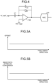
- FIG. 4 is a diagram illustrating the detail of a periphery of the PGA 150.
- the offset giving unit 15 includes a plurality of PGAs 150 as in the foregoing.
- the offset generator 152 generates the offset voltage necessary to prevent the saturation of the signal on the black side of the A/D converter 140, which is set such that the signal is not saturated even when noise arises on the signal. Because the non-inverting input (the non-inverting input terminal) of each of the PGAs 150 is configured, for example, as a gate of a MOS transistor and is of high impedance, a steady current does not flow in the wiring 154. Consequently, the offset voltages applied to the non-inverting inputs of the respective PGAs 150 are substantially the same. Thus, the current that steadily flows in the wiring 154 is substantially zero, and therefore, even when the offset voltage is supplied from the offset generator 152 in the array direction (left-to-right direction) of the light receiving elements 120, the voltage does not drop.
- the PGA 150 when a reset level (V_rst) is input from the light receiving element 120 into an inverting input (an inverting input terminal), the SW1 is turned on, the inverting input terminal and an output terminal are short-circuited, and the inverting input terminal and the output terminal are both at a voltage level of Vpga.
- V_sig signal level
- FIG. 5A is a diagram illustrating an offset voltage output from each of the PGAs 150 that are arrayed in the pixel array direction
- FIG. 5B is a diagram illustrating the result of A/D conversion that each of a plurality of A/D converters 140 performed the A/D conversion on an image signal of uniform density.
- the offset voltage given by the respective PGAs 150 is of a fixed voltage (Vpga).
- the photoelectric conversion device 10 can apply a substantially identical offset voltage to each pixel (or each column), and thus it can also prevent the saturation of the signal on the black side of the A/D converter 140 due to the drop of the offset voltage.
- FIGS. 6A and 6B are diagrams illustrating the relation between a reference voltage of an A/D converter and image data after A/D conversion according to a comparative example.
- the reference voltage of a plurality of A/D converters is supplied from one end in the pixel array direction toward the other end by wiring, because the load of the A/D converter is large and a large current to some extent flows, the reference voltage of the A/D converter may vary by the impedance of the wiring.
- Vrefp is a reference voltage on the top side (the upper side) of the A/D converter
- Vrefn is a reference voltage on the bottom side (the lower side).
- the image data after A/D conversion results in an ever-increasing distribution, and thus the black level is to hold an ever-increasing distribution.
- FIG. 7 is a block diagram illustrating the detail and the periphery of the offset giving unit 15 (an offset giving unit 15a) according to a first modification.
- the offset giving unit 15a includes the PGAs 150, the offset generator 152, the wiring 154, and a load 156.
- a reference voltage generator (a reference voltage source) 142 generates a reference voltage (Vrefp, Vrefn) for each of the A/D converters 140, and applies the reference voltage to the respective A/D converters 140 through wiring 144 (first wiring).
- the offset generator 152 and the reference voltage generator 142 are disposed on one end side of the array of the light receiving elements 120, and the load 156 is disposed on the other end side of the array of the light receiving elements 120.
- the load 156 is connected to the wiring 154, and is a pseudo-load that functions such that the current by the offset voltage generated by the offset generator 152 steadily flows in the wiring 154. That is, when the reference voltage varies depending on the length of the wiring 144 from the reference voltage generator 142, the load 156 makes the current steadily flow into the wiring 154 from the offset generator 152 by being connected to the wiring 154 and varies the offset voltage depending on the length of the wiring 154 from the offset generator 152 so as to offset the variation of the reference voltage.
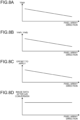
- FIGS. 8A to 8D are diagrams illustrating an example of the operation of the photoelectric conversion device 10 that includes the offset giving unit 15a illustrated in FIG. 7 .
- the offset voltage Vpga of the wiring 154 holds a distribution declining from the left-hand side in the pixel array direction toward the right-hand side.
- the reference voltage (Vrefp, Vrefn) holds a distribution declining from the left-hand side in the pixel array direction toward the right-hand side.
- the offset voltage applied to each PGA 150 also holds a distribution declining from the left-hand side in the pixel array direction toward the right-hand side.
- the load 156 forms a distribution of the offset voltage of the wiring 154 so as to offset the distribution of the reference voltage of the wiring 144. That is, when a distribution arises in the reference voltage of the wiring 144, the offset giving unit 15a makes the distribution of the offset voltage arise in the wiring 154.
- FIG. 8D when A/D conversion is performed on an image signal of uniform density, pieces of the image data from the respective A/D converters 140 after the A/D conversion are substantially identical.
- Vpga Vrefn + ⁇ ( ⁇ is a value that prevents the image signal from being below Vrefn even when noise occurs in a pixel circuit and other parts), the saturation of the signal on the bottom side of the A/D converter 140 is prevented.
- FIG. 9 is a block diagram illustrating the detail and the periphery of the offset giving unit 15 (an offset giving unit 15b) according to the preferred embodiment of the invention.
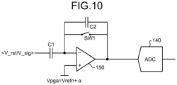
- FIG. 10 is a diagram illustrating the detail of a periphery of the PGA 150 in the offset giving unit 15b.
- the offset giving unit 15b includes the PGAs 150 and a plurality of offset generators 158.
- the reference voltage generator 142 generates the reference voltage (Vrefp, Vrefn) for the A/D converters 140, and applies the reference voltage to the respective A/D converters 140 through the wiring 144 (the first wiring).
- the reference voltage generator 142 further applies a certain reference voltage to the offset generators 158 through the wiring 144.
- the offset generators 158 each input, by using the reference voltage applied from the reference voltage generator 142, a certain offset voltage to the non-inverting input terminals of the respective PGAs 150.
- the offset generators 158 each generate the offset voltage by making a certain amount of shift in voltage with respect to the reference voltage that is applied to the respective A/D converters 140 through the wiring 144.
- FIGS. 11A to 11D are diagrams illustrating an example of the operation of the photoelectric conversion device 10 that includes the offset giving unit 15b illustrated in FIG. 9 .
- the offset voltage that is applied to the image signals output from the respective light receiving elements 120 is also lowered in the same manner. Consequently, in the photoelectric conversion device 10 that includes the offset giving unit 15b, as the same as the operation that is illustrated in FIGS. 8A to 8D , when A/D conversion is performed on image signals of uniform density, pieces of the image data from the A/D converters 140 after the A/D conversion are substantially identical.
- the photoelectric conversion device 10 includes the light receiving elements 120 that are arrayed in the one direction for each color of R, G, and B, a single column contains three light receiving elements 120 of R, G, and B, and the A/D conversion is performed, for each column, on a photoelectric converted signal, for example.
- the gain of the corresponding PGA 150 may be switched for each color.
- FIGS. 12A and 12B are diagrams illustrating an example of signal levels, which may arise when the gain is switched for each color, on the black side of the A/D converter.
- FIG. 12A illustrates an example of a state that the signal level on the black side of the A/D converter 140 is not saturated.
- FIG. 12B illustrates an example of a state that the signal level on the black side of the A/D converter 140 is saturated.
- the gain before the A/D conversion is different for each color, it is conceivable that the signal on the black side is saturated at the input of the A/D converter 140.
- the setting gain of the PGA 150 is different for each color and the noise width of the black level is different for each color, if the offset level in each color is made identical, the saturation in the color of a small gain can be prevented by applying an offset voltage Vrefn + ⁇ , but in the color of a large gain, the black level may be saturated to the bottom side even when the offset voltage Vrefn + ⁇ is applied. That is, when the black level is saturated to the bottom side, the gradation on the black side cannot be ensured.
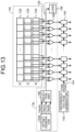
- FIG. 13 is a block diagram illustrating the detail and the periphery of the offset giving unit 15 (an offset giving unit 15c) that switches the offset voltage for each color according to a second modification.
- a photoelectric conversion unit 12a includes the light receiving elements 120 arrayed in the one direction for each color of R, G, and B of receiving light.
- the offset giving unit 15c includes the PGAs 150, an offset generator 152a, a selection unit 159, the wiring 154, and the load 156.
- the A/D converters 140 perform A/D conversion on electrical signals output from the respective light receiving elements 120 that receive light of different colors.
- the offset generator 152a generates different offset voltages Ofs(R), Ofs(G), and Ofs(B) for each color of R, G, and B, respectively, and outputs them to the selection unit 159.
- the selection unit 159 selects, out of Ofs(R), Ofs(G), and Ofs(B), an offset voltage corresponding to the light receiving element 120 that received the light in any of the colors of R, G, and B in a column outputting the image signal.
- the selection unit 159 may be configured as a switching unit that switches the offset voltages that the offset giving unit 15c gives (or the offset voltages that the offset generator 152a generates) for each color received by the light receiving elements 120.
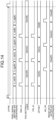
- FIG. 14 is a timing chart illustrating operation timing of the photoelectric conversion device 10 that includes the offset giving unit 15c. As illustrated in FIG. 14 , it is assumed that image signals (pixel signals) on which the light receiving elements 120 performed photoelectric conversion are output to the PGAs 150 in order of R, G, and B. LSYNC is a line synchronization signal. Gain_ch is a gain switching signal. Ofs_ch is an offset switching signal. AD_CK is a clock signal for A/D conversion in the A/D converters 140.
- the timing controller 16 switches, for the PGAs 150, the gain to the gain for R, Gain(R), at the timing that a reset level V_rst(R) of the light receiving elements 120 for R is output.
- the timing controller 16 controls the selection unit 159 so as to switch the offset voltage of the PGA 150 to an offset voltage for R, Ofs(R).
- the timing controller 16 makes, at the timing that an image signal for R, V_sig(R), is being output, the A/D converters 140 perform A/D conversion and generate image data, Data(R).
- the photoelectric conversion device 10 performs the same operation for G and B also.
- FIGS. 15A and 15B are diagrams illustrating an example of signal levels on the black side of the A/D converters 140 when the photoelectric conversion device 10 including the offset giving unit 15c switches the gain for each color. For example, when the gain for G out of R, G, and B is small and the gain for R is large, the photoelectric conversion device 10 including the offset giving unit 15c adds Ofs(G) at the time the signal of G is input as illustrated in FIG. 15A , and adds Ofs(R) at the time the signal of R is input as illustrated in FIG. 15B .
- the photoelectric conversion device 10 including the offset giving unit 15c can change the offset level for each color, even when the gain of the PGAs 150 is switched and the noise width of the black level is different for each color, this configuration can prevent the saturation of the signal level on the black side.
- FIG. 16 is a block diagram illustrating an overview of an image forming apparatus 50 provided with an image reading apparatus 60 including the photoelectric conversion device 10.
- the image forming apparatus 50 is a copying machine and a multifunction peripheral (MFP) that includes the image reading apparatus 60 and an image forming unit 70, for example.
- MFP multifunction peripheral
- the image reading apparatus 60 includes the photoelectric conversion device 10, an LED driver (LED_DRV) 600, and an LED 602, for example.
- the LED driver 600 drives the LED 602, in synchronization with a line synchronization signal that the timing controller 16 outputs, for example.
- the LED 602 irradiates a document with light.
- the light receiving elements 120 receive reflection light from the document, generate electrical charges, and start accumulating the electrical charges.
- the photoelectric conversion device 10 then outputs image data to the image forming unit 70 after performing parallel-to-serial conversion and others.
- the image forming unit 70 includes a processing unit 80 and a printer engine 82.
- the processing unit 80 and the printer engine 82 are connected through an interface (I/F) 84.
- the processing unit 80 includes an LVDS 800, an image processor 802, and the CPU 11.
- the CPU 11 executes programs stored in a memory and others, and controls various units constituting the image forming apparatus 50 such as the photoelectric conversion device 10.
- the photoelectric conversion device 10 outputs, to the LVDS 800, image data of an image that the image reading apparatus 60 reads, a line synchronization signal, a transmission clock, and other signals, for example.
- the LVDS 800 converts the received image data, the line synchronization signal, the transmission clock, and other signals into 10-bit parallel data.
- the image processor 802 performs image processing by using the converted 10-bit data, and outputs image data and other signals to the printer engine 82.
- the printer engine 82 prints by using the received image data.
- Processing circuitry includes a programmed processor, as a processor includes circuitry.
- a processing circuit also includes devices such as an application specific integrated circuit (ASIC), digital signal processor (DSP), field programmable gate array (FPGA) and conventional circuit components arranged to perform the recited functions.
- ASIC application specific integrated circuit
- DSP digital signal processor
- FPGA field programmable gate array
Landscapes
- Engineering & Computer Science (AREA)
- Multimedia (AREA)
- Signal Processing (AREA)
- Facsimile Heads (AREA)
- Transforming Light Signals Into Electric Signals (AREA)
- Solid State Image Pick-Up Elements (AREA)
Claims (6)
- Photoelektrische Umwandlungsvorrichtung (10), die umfasst:eine Vielzahl von Lichtempfangselementen (120), die in einer Richtung angeordnet sind und jeweils ein Lichtsignal in ein elektrisches Signal V_sig umwandeln;eine Vielzahl von A/D-Wandlereinheiten (140), die eine A/D-Wandlung der von den Lichtempfangselementen (120) ausgegebenen elektrischen Signale V_sig durchführen; undeine Offset-Gebereinheit (15b), die so konfiguriert ist, dass sie den elektrischen Signalen V_sig, die von den Lichtempfangselementen (120) ausgegeben werden, eine Offset-Spannung Vpga aufgibt, bevor die elektrischen Signale V_sig in die A/D-Wandlereinheiten (140) eingegeben werden,dadurch gekennzeichnet, dass:die A/D-Wandlereinheiten (140) in der einen Richtung entlang der Lichtempfangselemente (120) angeordnet sind und über eine erste Verdrahtung (144), die sich in der einen Richtung von einer Referenzspannungsquelle (142) erstreckt, mit einer Referenzspannung Vrefn versorgt werden, die an einer Endseite der Anordnung angeordnet sind, unddie Offset-geberinheit (15b) weiterhin umfasst:mehrere Offset-Generatoren (158), die jeweils die Offset-Spannung Vpga erzeugen, deren Spannung um einen Betrag α in Bezug auf die Referenzspannung Vrefn verschoben ist, die durch die erste Verdrahtung (144) an die A/D-Wandlereinheiten (140) und an die mehreren Generatoren (158) angelegt wird, wobei der Betrag α ein Wert ist, der verhindert, dass das Bildsignal unter die Referenzspannung Vrefn fällt, undeine Vielzahl von Verstärkern (150), die jeweilsüber ihren jeweiligen nicht-invertierenden Eingangsanschluss die vom jeweiligen Offset-Generator (158) erzeugte Offset-Spannung Vpga empfangen,über ihren jeweiligen invertierenden Eingangsanschluss das von den Lichtempfangselementen (120) ausgegebene elektrische Signal V_sig empfangen, unddas elektrische Signal an die jeweilige A/D-Wandlereinheit (140) ausgeben.
- Photoelektrische Umwandlungsvorrichtung (10) nach Anspruch 1, wobeidie Lichtempfangselemente (120) für jede Farbe des Empfangslichts in einer Richtung angeordnet sind, unddie A/D-Wandlereinheiten (140) eine A/D-Wandlung der elektrischen Signale durchführen, die von den Lichtempfangselementen (120) ausgegeben werden, die Licht unterschiedlicher Farben empfangen.
- Photoelektrische Umwandlungsvorrichtung (10) nach Anspruch 2, die weiterhin eine Schalteinheit (159) umfasst, die zum Schalten von Offsetspannungen konfiguriert ist, die die Offset-Gebereinheit (15b) für jede Farbe liefert, die das Lichtempfangselement (120) empfängt.
- Bildlesegerät (60), das die fotoelektrische Umwandlungsvorrichtung (10) nach einem der Ansprüche 1 bis 3 umfasst.
- Bilderzeugungsgerät (50), das umfasst:das Bildlesegerät (60) nach Anspruch 4; undeine Bilderzeugungseinheit (70), die ein Bild basierend auf Bilddaten erzeugt, die von der Bildlesevorrichtung (60) gelesen werden.
- Verfahren zur fotoelektrischen Umwandlung, das in einer fotoelektrischen Umwandlungsvorrichtung (10) durchgeführt wird, das Folgende umfasst:eine Vielzahl von Lichtempfangselementen (120), die in einer Richtung angeordnet sind und jeweils ein Lichtsignal in ein elektrisches Signal umwandeln; undeine Vielzahl von A/D-Wandlereinheiten (140), die eine A/D-Wandlung der von den Lichtempfangselementen (120) ausgegebenen elektrischen Signale V_sig durchführen,wobei das Verfahren Folgendes umfasst:Anlegen einer Offsetspannung Vpga an die von den Lichtempfangselementen (120) ausgegebenen elektrischen Signale V_sig, bevor die elektrischen Signale V_sig in die A/D-Wandlereinheiten (140) eingegeben werden;gekennzeichnet durch:Anlegen einer Referenzspannung Vrefn an die A/D-Wandlereinheiten (140), die in der einen Richtung entlang der Lichtempfangselemente (120) angeordnet sind, über eine erste Verdrahtung (144), die sich in der einen Richtung von einer Referenzspannungsquelle (142) erstreckt, die an einer Endseite der Anordnung angeordnet ist, undErzeugen einer Offset-Spannung Vpga durch jeden von mehreren Offset-Generatoren (158), die um einen Spannungsbetrag α in Bezug auf die Referenzspannung Vrefn verschoben ist, die an die A/D-Wandlereinheiten (140) und an die mehreren Generatoren (158) angelegt wird, über die erste Verdrahtung (144), wobei der Betrag α ein Wert ist, der verhindert, dass das Bildsignal unter der Referenzspannung Vref n liegt,Empfangen der vom jeweiligen Offsetgenerator (158) erzeugten Offsetspannung Vpga durch jeden aus einer Vielzahl von Verstärkern (150) über seinen jeweiligen nicht-invertierenden Eingangsanschluss,Empfangen der von den Lichtempfangselementen (120) ausgegebenen elektrischen Signale V_sig durch jeden der mehreren Verstärker (150) über seinen jeweiligen invertierenden Eingangsanschluss, undAusgeben des elektrischen Signals durch jeden der mehreren Verstärker (150) an die jeweilige A/D-Wandlereinheit (140).
Applications Claiming Priority (2)
| Application Number | Priority Date | Filing Date | Title |
|---|---|---|---|
| JP2015121471A JP6544070B2 (ja) | 2015-06-16 | 2015-06-16 | 光電変換素子、画像読取装置及び画像形成装置 |
| EP16174603.7A EP3107280A3 (de) | 2015-06-16 | 2016-06-15 | Vorrichtung zur fotoelektrischen umwandlung, bildlesevorrichtung, bilderzeugungsvorrichtung und verfahren zur fotoelektrischen umwandlung |
Related Parent Applications (1)
| Application Number | Title | Priority Date | Filing Date |
|---|---|---|---|
| EP16174603.7A Division EP3107280A3 (de) | 2015-06-16 | 2016-06-15 | Vorrichtung zur fotoelektrischen umwandlung, bildlesevorrichtung, bilderzeugungsvorrichtung und verfahren zur fotoelektrischen umwandlung |
Publications (2)
| Publication Number | Publication Date |
|---|---|
| EP3637760A1 EP3637760A1 (de) | 2020-04-15 |
| EP3637760B1 true EP3637760B1 (de) | 2024-07-31 |
Family
ID=56134200
Family Applications (2)
| Application Number | Title | Priority Date | Filing Date |
|---|---|---|---|
| EP19213636.4A Active EP3637760B1 (de) | 2015-06-16 | 2016-06-15 | Vorrichtung zur fotoelektrischen umwandlung, bildlesevorrichtung, bilderzeugungsvorrichtung und verfahren zur fotoelektrischen umwandlung |
| EP16174603.7A Withdrawn EP3107280A3 (de) | 2015-06-16 | 2016-06-15 | Vorrichtung zur fotoelektrischen umwandlung, bildlesevorrichtung, bilderzeugungsvorrichtung und verfahren zur fotoelektrischen umwandlung |
Family Applications After (1)
| Application Number | Title | Priority Date | Filing Date |
|---|---|---|---|
| EP16174603.7A Withdrawn EP3107280A3 (de) | 2015-06-16 | 2016-06-15 | Vorrichtung zur fotoelektrischen umwandlung, bildlesevorrichtung, bilderzeugungsvorrichtung und verfahren zur fotoelektrischen umwandlung |
Country Status (3)
| Country | Link |
|---|---|
| US (2) | US10356272B2 (de) |
| EP (2) | EP3637760B1 (de) |
| JP (1) | JP6544070B2 (de) |
Families Citing this family (24)
| Publication number | Priority date | Publication date | Assignee | Title |
|---|---|---|---|---|
| JP6432332B2 (ja) * | 2014-12-15 | 2018-12-05 | 株式会社リコー | 光電変換素子、画像読取装置及び画像形成装置 |
| JP6699305B2 (ja) | 2016-04-07 | 2020-05-27 | 株式会社リコー | 信号処理装置、光電変換素子、画像読取装置、画像形成装置及び信号処理方法 |
| US10182177B2 (en) | 2016-04-15 | 2019-01-15 | Ricoh Company, Ltd. | Signal processing device, image scanning device, image forming apparatus, and method of controlling the same |
| JP6822096B2 (ja) | 2016-11-24 | 2021-01-27 | 株式会社リコー | 光電変換装置、光電変換方法及び画像形成装置 |
| JP6880709B2 (ja) | 2016-12-20 | 2021-06-02 | 株式会社リコー | 光電変換装置、光電変換方法及び画像形成装置 |
| US10542184B2 (en) | 2017-01-25 | 2020-01-21 | Ricoh Company, Ltd. | Photoelectric conversion device, defective pixel determining method, image forming apparatus, and recording medium |
| JP6946983B2 (ja) | 2017-11-30 | 2021-10-13 | 株式会社リコー | 位置検出装置、画像読取装置、画像形成装置、プログラムおよび位置検出方法 |
| JP7056176B2 (ja) | 2018-01-26 | 2022-04-19 | 株式会社リコー | 位置検出装置、画像形成装置、および位置検出方法 |
| JP7043852B2 (ja) | 2018-01-26 | 2022-03-30 | 株式会社リコー | 位置検出装置、画像形成装置、および方法 |
| JP2019129514A (ja) | 2018-01-26 | 2019-08-01 | 株式会社リコー | 画像読取装置、画像形成装置および濃度補正方法 |
| JP7159568B2 (ja) | 2018-02-23 | 2022-10-25 | 株式会社リコー | 光電変換素子、画像読取装置、および画像形成装置 |
| JP7010131B2 (ja) | 2018-04-24 | 2022-01-26 | 株式会社リコー | 色検査装置、画像形成装置、色検査方法およびプログラム |
| JP7081286B2 (ja) | 2018-04-27 | 2022-06-07 | 株式会社リコー | 読取装置、画像形成装置、情報検出方法、およびプログラム |
| CN110830670A (zh) | 2018-08-10 | 2020-02-21 | 株式会社理光 | 读取装置、图像形成装置、真伪判定系统及读取方法 |
| CN110830675B (zh) | 2018-08-10 | 2022-05-03 | 株式会社理光 | 读取装置、图像形成装置及读取方法 |
| JP7115206B2 (ja) | 2018-10-11 | 2022-08-09 | 株式会社リコー | 原稿サイズ検出装置、画像読取装置、画像形成装置、及び原稿サイズ検出方法 |
| JP7183682B2 (ja) | 2018-10-12 | 2022-12-06 | 株式会社リコー | 読取装置、画像読取装置、画像形成装置、及び読取方法 |
| JP7314752B2 (ja) | 2019-09-30 | 2023-07-26 | 株式会社リコー | 光電変換素子、読取装置、画像処理装置および光電変換素子の製造方法 |
| JP7400480B2 (ja) | 2020-01-14 | 2023-12-19 | 株式会社リコー | 画像読取装置および画像読取方法 |
| JP7592974B2 (ja) | 2020-03-05 | 2024-12-03 | 株式会社リコー | 読取装置、画像処理装置および特徴量検出方法 |
| JP7452268B2 (ja) | 2020-06-08 | 2024-03-19 | 株式会社リコー | 位置検出装置、画像形成装置および位置検出方法 |
| JP7468176B2 (ja) | 2020-06-17 | 2024-04-16 | 株式会社リコー | 画像処理装置および画像読取方法 |
| JP7559377B2 (ja) | 2020-06-25 | 2024-10-02 | 株式会社リコー | 固体撮像素子、読取装置、画像処理装置および制御方法 |
| JP7593019B2 (ja) | 2020-09-16 | 2024-12-03 | 株式会社リコー | 画像形成装置、及び画像形成方法 |
Family Cites Families (45)
| Publication number | Priority date | Publication date | Assignee | Title |
|---|---|---|---|---|
| US6344877B1 (en) * | 1997-06-12 | 2002-02-05 | International Business Machines Corporation | Image sensor with dummy pixel or dummy pixel array |
| US6838651B1 (en) * | 2002-03-28 | 2005-01-04 | Ess Technology, Inc. | High sensitivity snap shot CMOS image sensor |
| US7408683B2 (en) | 2002-07-15 | 2008-08-05 | Brother Kogyo Kabushiki Kaisha | Image sensor for reading image and image reading apparatus including the image sensor |
| JP2004048549A (ja) | 2002-07-15 | 2004-02-12 | Brother Ind Ltd | イメージセンサ及びそれを用いた画像読取装置 |
| JP2005101985A (ja) | 2003-09-25 | 2005-04-14 | Sony Corp | 固体撮像装置および画像入力装置 |
| JP2006109349A (ja) * | 2004-10-08 | 2006-04-20 | Ricoh Co Ltd | 定電流回路及びその定電流回路を使用したシステム電源装置 |
| US7630103B2 (en) | 2005-03-16 | 2009-12-08 | Kabushiki Kaisha Toshiba | Image reading apparatus and image forming apparatus |
| JP4565567B2 (ja) | 2006-02-07 | 2010-10-20 | 株式会社リコー | アナログ信号バッファ、アナログ信号処理システム、画像読取装置、及び画像形成装置 |
| JP4971834B2 (ja) * | 2007-03-01 | 2012-07-11 | キヤノン株式会社 | 撮像装置及び撮像システム |
| JP4699417B2 (ja) | 2007-04-16 | 2011-06-08 | 株式会社リコー | アナログ処理回路およびアナログ集積回路装置および画像読取装置および画像形成装置 |
| JP2008271159A (ja) * | 2007-04-19 | 2008-11-06 | Matsushita Electric Ind Co Ltd | 固体撮像装置 |
| JP4353275B2 (ja) * | 2007-05-22 | 2009-10-28 | セイコーエプソン株式会社 | アナログフロントエンド回路及び電子機器 |
| US7561090B1 (en) * | 2008-01-03 | 2009-07-14 | The Boeing Company | Focal plane array with serial, variable bit width analog to digital converter |
| JP5347341B2 (ja) | 2008-06-06 | 2013-11-20 | ソニー株式会社 | 固体撮像装置、撮像装置、電子機器、ad変換装置、ad変換方法 |
| JP5444795B2 (ja) | 2008-07-29 | 2014-03-19 | 株式会社リコー | 画像読み取り装置、画像形成装置、振幅調整方法、及びコンピュータプログラム |
| JP2010103911A (ja) | 2008-10-27 | 2010-05-06 | Canon Inc | 画像読取装置 |
| JP5206423B2 (ja) | 2009-01-07 | 2013-06-12 | 株式会社リコー | 画像読み取り装置、画像形成装置、及びサンプル・ホールド制御方法 |
| JP2011024109A (ja) * | 2009-07-17 | 2011-02-03 | Panasonic Corp | 固体撮像装置およびそれを備えるカメラ |
| JP5326911B2 (ja) | 2009-07-30 | 2013-10-30 | 株式会社リコー | スペクトラム拡散クロックジェネレータ、回路装置、画像読取装置、画像形成装置、及びスペクトラム拡散クロック生成方法 |
| JP5454019B2 (ja) | 2009-09-02 | 2014-03-26 | 株式会社リコー | 光電変換素子、センサ制御回路、画像読取装置、及び画像形成装置 |
| JP5476876B2 (ja) | 2009-09-11 | 2014-04-23 | 株式会社リコー | センサ駆動回路、ドライバ装置、画像読取装置、及び画像形成装置 |
| JP5493980B2 (ja) * | 2010-02-19 | 2014-05-14 | ソニー株式会社 | 固体撮像素子、およびカメラシステム |
| JP5633860B2 (ja) | 2010-07-06 | 2014-12-03 | 株式会社リコー | アナログ信号バッファおよび画像読取装置 |
| JP5115602B2 (ja) | 2010-08-06 | 2013-01-09 | ソニー株式会社 | 半導体装置およびその制御方法 |
| JP5716346B2 (ja) | 2010-10-13 | 2015-05-13 | 株式会社リコー | 信号バッファ回路とセンサ制御基板と画像読取装置および画像形成装置 |
| KR20120058057A (ko) * | 2010-11-29 | 2012-06-07 | 삼성전자주식회사 | 오프셋 제거 회로, 샘플링 회로 및 이미지 센서 |
| US8405747B2 (en) * | 2011-02-17 | 2013-03-26 | Omnivision Technologies, Inc. | Analog row black level calibration for CMOS image sensor |
| JP5724463B2 (ja) | 2011-03-03 | 2015-05-27 | 株式会社リコー | 信号処理回路と画像読取装置および画像形成装置 |
| JP2012237780A (ja) * | 2011-05-10 | 2012-12-06 | Konica Minolta Business Technologies Inc | 画像形成装置 |
| JP6226508B2 (ja) | 2011-09-13 | 2017-11-08 | 株式会社リコー | 画像読取装置、画像形成装置及び画像読取方法 |
| JP6051654B2 (ja) | 2012-07-25 | 2016-12-27 | 株式会社リコー | 画像読取装置、及び画像形成装置 |
| KR101570562B1 (ko) | 2012-12-28 | 2015-11-19 | 제일모직주식회사 | 폴리아미드 수지, 이의 제조방법 및 이를 포함하는 성형품 |
| JP6146015B2 (ja) | 2013-01-18 | 2017-06-14 | 株式会社リコー | 光電変換素子、画像読取装置及び画像形成装置 |
| JP6127536B2 (ja) | 2013-01-24 | 2017-05-17 | 株式会社リコー | 画像読取装置、画像形成装置及び画像読取方法 |
| JP6149408B2 (ja) | 2013-01-29 | 2017-06-21 | 株式会社リコー | 固体撮像素子、画像読取装置及び画像形成装置 |
| JP6205885B2 (ja) | 2013-06-18 | 2017-10-04 | 株式会社リコー | 光電変換素子、画像読取装置、画像形成装置及び画像読取方法 |
| JP6260135B2 (ja) | 2013-08-06 | 2018-01-17 | 株式会社リコー | 光電変換素子、画像読取装置及び画像形成装置 |
| JP6383143B2 (ja) | 2013-10-08 | 2018-08-29 | 株式会社リコー | 撮像素子、画像読取装置、画像形成装置及び撮像方法 |
| JP6287058B2 (ja) | 2013-10-24 | 2018-03-07 | 株式会社リコー | 縮小光学系用の光電変換素子、画像読取装置、画像形成装置及び画像読取方法 |
| JP6225682B2 (ja) | 2013-12-11 | 2017-11-08 | 株式会社リコー | 撮像素子、画像読取装置及び画像形成装置 |
| JP6281304B2 (ja) | 2014-02-04 | 2018-02-21 | 株式会社リコー | 撮像素子、画像読取装置及び画像形成装置 |
| JP6519997B2 (ja) | 2014-07-04 | 2019-05-29 | 株式会社リコー | 光電変換素子、画像読取装置及び画像形成装置 |
| JP6451104B2 (ja) | 2014-07-04 | 2019-01-16 | 株式会社リコー | 光電変換素子、画像読取装置、画像形成装置及び信号制御方法 |
| JP6549366B2 (ja) | 2014-09-19 | 2019-07-24 | 株式会社リコー | 光電変換素子、画像読取装置及び画像形成装置 |
| JP2017126833A (ja) * | 2016-01-12 | 2017-07-20 | 株式会社リコー | 光電変換素子、画像読取装置、画像形成装置及び画像読取方法 |
-
2015
- 2015-06-16 JP JP2015121471A patent/JP6544070B2/ja active Active
-
2016
- 2016-06-08 US US15/176,395 patent/US10356272B2/en active Active
- 2016-06-15 EP EP19213636.4A patent/EP3637760B1/de active Active
- 2016-06-15 EP EP16174603.7A patent/EP3107280A3/de not_active Withdrawn
-
2019
- 2019-05-31 US US16/427,946 patent/US10554849B2/en active Active
Also Published As
| Publication number | Publication date |
|---|---|
| US20190289163A1 (en) | 2019-09-19 |
| EP3637760A1 (de) | 2020-04-15 |
| EP3107280A3 (de) | 2017-02-22 |
| US10554849B2 (en) | 2020-02-04 |
| EP3107280A2 (de) | 2016-12-21 |
| JP6544070B2 (ja) | 2019-07-17 |
| JP2017011339A (ja) | 2017-01-12 |
| US20160373604A1 (en) | 2016-12-22 |
| US10356272B2 (en) | 2019-07-16 |
Similar Documents
| Publication | Publication Date | Title |
|---|---|---|
| US10554849B2 (en) | Photoelectric conversion device, image reading apparatus, image forming apparatus, and method of photoelectric conversion | |
| US11019293B2 (en) | Photoelectric conversion element, image reading device, image forming apparatus, and signal control method | |
| US10298866B2 (en) | Photoelectric conversion element, image reading device, image forming apparatus, image reading method, and computer-readable recording medium | |
| JP4699417B2 (ja) | アナログ処理回路およびアナログ集積回路装置および画像読取装置および画像形成装置 | |
| US9429470B2 (en) | Opto-electronic converter, image reading device, and image forming apparatus | |
| US10721373B2 (en) | Image sensing device, image reading device, image forming apparatus and image sensing method | |
| US9628654B2 (en) | Processing device, image reading device, image forming apparatus, and processing method | |
| JP6699305B2 (ja) | 信号処理装置、光電変換素子、画像読取装置、画像形成装置及び信号処理方法 | |
| US9762826B2 (en) | Photoelectric conversion element, image reading device, image forming apparatus, and photoelectric conversion method | |
| US8692920B2 (en) | Solid-state imaging apparatus, A/D converter, and control method thereof | |
| US7656329B2 (en) | Time-interleaved analog-to-digital conversion apparatus | |
| US8339495B2 (en) | Solid-state image pickup apparatus and method for driving solid-state image pickup apparatus | |
| EP2552117B1 (de) | Fotoelektrischer Wandler, Bildlesevorrichtung und Bildleseverfahren | |
| JP6295667B2 (ja) | A/d変換器、撮像素子、画像読取装置及び画像形成装置 | |
| JP4121981B2 (ja) | 画像読取装置 | |
| JP6409364B2 (ja) | 光電変換素子、画像読取装置、画像形成装置、調整方法及び調整プログラム | |
| US8593324B2 (en) | Analog-to-digital converting circuit and analog-to-digital converting method | |
| JP2006217453A (ja) | 映像信号処理装置 |
Legal Events
| Date | Code | Title | Description |
|---|---|---|---|
| PUAI | Public reference made under article 153(3) epc to a published international application that has entered the european phase |
Free format text: ORIGINAL CODE: 0009012 |
|
| STAA | Information on the status of an ep patent application or granted ep patent |
Free format text: STATUS: REQUEST FOR EXAMINATION WAS MADE |
|
| 17P | Request for examination filed |
Effective date: 20191204 |
|
| AC | Divisional application: reference to earlier application |
Ref document number: 3107280 Country of ref document: EP Kind code of ref document: P |
|
| AK | Designated contracting states |
Kind code of ref document: A1 Designated state(s): AL AT BE BG CH CY CZ DE DK EE ES FI FR GB GR HR HU IE IS IT LI LT LU LV MC MK MT NL NO PL PT RO RS SE SI SK SM TR |
|
| STAA | Information on the status of an ep patent application or granted ep patent |
Free format text: STATUS: EXAMINATION IS IN PROGRESS |
|
| 17Q | First examination report despatched |
Effective date: 20210615 |
|
| REG | Reference to a national code |
Ref country code: DE Ref legal event code: R079 Free format text: PREVIOUS MAIN CLASS: H04N0005369000 Ipc: H04N0025630000 Ref country code: DE Ref legal event code: R079 Ref document number: 602016088712 Country of ref document: DE Free format text: PREVIOUS MAIN CLASS: H04N0005369000 Ipc: H04N0025630000 |
|
| GRAP | Despatch of communication of intention to grant a patent |
Free format text: ORIGINAL CODE: EPIDOSNIGR1 |
|
| STAA | Information on the status of an ep patent application or granted ep patent |
Free format text: STATUS: GRANT OF PATENT IS INTENDED |
|
| RIC1 | Information provided on ipc code assigned before grant |
Ipc: H04N 25/78 20230101ALI20240129BHEP Ipc: H04N 25/60 20230101ALI20240129BHEP Ipc: H04N 1/193 20060101ALI20240129BHEP Ipc: H04N 25/75 20230101ALI20240129BHEP Ipc: H04N 25/701 20230101ALI20240129BHEP Ipc: H04N 25/671 20230101ALI20240129BHEP Ipc: H04N 25/63 20230101AFI20240129BHEP |
|
| INTG | Intention to grant announced |
Effective date: 20240222 |
|
| P01 | Opt-out of the competence of the unified patent court (upc) registered |
Effective date: 20240418 |
|
| GRAS | Grant fee paid |
Free format text: ORIGINAL CODE: EPIDOSNIGR3 |
|
| GRAA | (expected) grant |
Free format text: ORIGINAL CODE: 0009210 |
|
| STAA | Information on the status of an ep patent application or granted ep patent |
Free format text: STATUS: THE PATENT HAS BEEN GRANTED |
|
| AC | Divisional application: reference to earlier application |
Ref document number: 3107280 Country of ref document: EP Kind code of ref document: P |
|
| AK | Designated contracting states |
Kind code of ref document: B1 Designated state(s): AL AT BE BG CH CY CZ DE DK EE ES FI FR GB GR HR HU IE IS IT LI LT LU LV MC MK MT NL NO PL PT RO RS SE SI SK SM TR |
|
| REG | Reference to a national code |
Ref country code: CH Ref legal event code: EP Ref country code: GB Ref legal event code: FG4D |
|
| REG | Reference to a national code |
Ref country code: DE Ref legal event code: R096 Ref document number: 602016088712 Country of ref document: DE |
|
| REG | Reference to a national code |
Ref country code: IE Ref legal event code: FG4D |
|
| REG | Reference to a national code |
Ref country code: NL Ref legal event code: FP |
|
| REG | Reference to a national code |
Ref country code: LT Ref legal event code: MG9D |
|
| PG25 | Lapsed in a contracting state [announced via postgrant information from national office to epo] |
Ref country code: PT Free format text: LAPSE BECAUSE OF FAILURE TO SUBMIT A TRANSLATION OF THE DESCRIPTION OR TO PAY THE FEE WITHIN THE PRESCRIBED TIME-LIMIT Effective date: 20241202 |
|
| REG | Reference to a national code |
Ref country code: AT Ref legal event code: MK05 Ref document number: 1709673 Country of ref document: AT Kind code of ref document: T Effective date: 20240731 |
|
| PG25 | Lapsed in a contracting state [announced via postgrant information from national office to epo] |
Ref country code: PT Free format text: LAPSE BECAUSE OF FAILURE TO SUBMIT A TRANSLATION OF THE DESCRIPTION OR TO PAY THE FEE WITHIN THE PRESCRIBED TIME-LIMIT Effective date: 20241202 |
|
| PG25 | Lapsed in a contracting state [announced via postgrant information from national office to epo] |
Ref country code: NO Free format text: LAPSE BECAUSE OF FAILURE TO SUBMIT A TRANSLATION OF THE DESCRIPTION OR TO PAY THE FEE WITHIN THE PRESCRIBED TIME-LIMIT Effective date: 20241031 |
|
| PG25 | Lapsed in a contracting state [announced via postgrant information from national office to epo] |
Ref country code: FI Free format text: LAPSE BECAUSE OF FAILURE TO SUBMIT A TRANSLATION OF THE DESCRIPTION OR TO PAY THE FEE WITHIN THE PRESCRIBED TIME-LIMIT Effective date: 20240731 Ref country code: GR Free format text: LAPSE BECAUSE OF FAILURE TO SUBMIT A TRANSLATION OF THE DESCRIPTION OR TO PAY THE FEE WITHIN THE PRESCRIBED TIME-LIMIT Effective date: 20241101 Ref country code: PL Free format text: LAPSE BECAUSE OF FAILURE TO SUBMIT A TRANSLATION OF THE DESCRIPTION OR TO PAY THE FEE WITHIN THE PRESCRIBED TIME-LIMIT Effective date: 20240731 |
|
| PG25 | Lapsed in a contracting state [announced via postgrant information from national office to epo] |
Ref country code: BG Free format text: LAPSE BECAUSE OF FAILURE TO SUBMIT A TRANSLATION OF THE DESCRIPTION OR TO PAY THE FEE WITHIN THE PRESCRIBED TIME-LIMIT Effective date: 20240731 |
|
| PG25 | Lapsed in a contracting state [announced via postgrant information from national office to epo] |
Ref country code: LV Free format text: LAPSE BECAUSE OF FAILURE TO SUBMIT A TRANSLATION OF THE DESCRIPTION OR TO PAY THE FEE WITHIN THE PRESCRIBED TIME-LIMIT Effective date: 20240731 |
|
| PG25 | Lapsed in a contracting state [announced via postgrant information from national office to epo] |
Ref country code: IS Free format text: LAPSE BECAUSE OF FAILURE TO SUBMIT A TRANSLATION OF THE DESCRIPTION OR TO PAY THE FEE WITHIN THE PRESCRIBED TIME-LIMIT Effective date: 20241130 Ref country code: AT Free format text: LAPSE BECAUSE OF FAILURE TO SUBMIT A TRANSLATION OF THE DESCRIPTION OR TO PAY THE FEE WITHIN THE PRESCRIBED TIME-LIMIT Effective date: 20240731 |
|
| PG25 | Lapsed in a contracting state [announced via postgrant information from national office to epo] |
Ref country code: HR Free format text: LAPSE BECAUSE OF FAILURE TO SUBMIT A TRANSLATION OF THE DESCRIPTION OR TO PAY THE FEE WITHIN THE PRESCRIBED TIME-LIMIT Effective date: 20240731 |
|
| PG25 | Lapsed in a contracting state [announced via postgrant information from national office to epo] |
Ref country code: ES Free format text: LAPSE BECAUSE OF FAILURE TO SUBMIT A TRANSLATION OF THE DESCRIPTION OR TO PAY THE FEE WITHIN THE PRESCRIBED TIME-LIMIT Effective date: 20240731 Ref country code: RS Free format text: LAPSE BECAUSE OF FAILURE TO SUBMIT A TRANSLATION OF THE DESCRIPTION OR TO PAY THE FEE WITHIN THE PRESCRIBED TIME-LIMIT Effective date: 20241031 |
|
| PG25 | Lapsed in a contracting state [announced via postgrant information from national office to epo] |
Ref country code: RS Free format text: LAPSE BECAUSE OF FAILURE TO SUBMIT A TRANSLATION OF THE DESCRIPTION OR TO PAY THE FEE WITHIN THE PRESCRIBED TIME-LIMIT Effective date: 20241031 Ref country code: PL Free format text: LAPSE BECAUSE OF FAILURE TO SUBMIT A TRANSLATION OF THE DESCRIPTION OR TO PAY THE FEE WITHIN THE PRESCRIBED TIME-LIMIT Effective date: 20240731 Ref country code: NO Free format text: LAPSE BECAUSE OF FAILURE TO SUBMIT A TRANSLATION OF THE DESCRIPTION OR TO PAY THE FEE WITHIN THE PRESCRIBED TIME-LIMIT Effective date: 20241031 Ref country code: LV Free format text: LAPSE BECAUSE OF FAILURE TO SUBMIT A TRANSLATION OF THE DESCRIPTION OR TO PAY THE FEE WITHIN THE PRESCRIBED TIME-LIMIT Effective date: 20240731 Ref country code: IS Free format text: LAPSE BECAUSE OF FAILURE TO SUBMIT A TRANSLATION OF THE DESCRIPTION OR TO PAY THE FEE WITHIN THE PRESCRIBED TIME-LIMIT Effective date: 20241130 Ref country code: HR Free format text: LAPSE BECAUSE OF FAILURE TO SUBMIT A TRANSLATION OF THE DESCRIPTION OR TO PAY THE FEE WITHIN THE PRESCRIBED TIME-LIMIT Effective date: 20240731 Ref country code: GR Free format text: LAPSE BECAUSE OF FAILURE TO SUBMIT A TRANSLATION OF THE DESCRIPTION OR TO PAY THE FEE WITHIN THE PRESCRIBED TIME-LIMIT Effective date: 20241101 Ref country code: FI Free format text: LAPSE BECAUSE OF FAILURE TO SUBMIT A TRANSLATION OF THE DESCRIPTION OR TO PAY THE FEE WITHIN THE PRESCRIBED TIME-LIMIT Effective date: 20240731 Ref country code: ES Free format text: LAPSE BECAUSE OF FAILURE TO SUBMIT A TRANSLATION OF THE DESCRIPTION OR TO PAY THE FEE WITHIN THE PRESCRIBED TIME-LIMIT Effective date: 20240731 Ref country code: BG Free format text: LAPSE BECAUSE OF FAILURE TO SUBMIT A TRANSLATION OF THE DESCRIPTION OR TO PAY THE FEE WITHIN THE PRESCRIBED TIME-LIMIT Effective date: 20240731 Ref country code: AT Free format text: LAPSE BECAUSE OF FAILURE TO SUBMIT A TRANSLATION OF THE DESCRIPTION OR TO PAY THE FEE WITHIN THE PRESCRIBED TIME-LIMIT Effective date: 20240731 |
|
| PG25 | Lapsed in a contracting state [announced via postgrant information from national office to epo] |
Ref country code: DK Free format text: LAPSE BECAUSE OF FAILURE TO SUBMIT A TRANSLATION OF THE DESCRIPTION OR TO PAY THE FEE WITHIN THE PRESCRIBED TIME-LIMIT Effective date: 20240731 Ref country code: RO Free format text: LAPSE BECAUSE OF FAILURE TO SUBMIT A TRANSLATION OF THE DESCRIPTION OR TO PAY THE FEE WITHIN THE PRESCRIBED TIME-LIMIT Effective date: 20240731 Ref country code: SM Free format text: LAPSE BECAUSE OF FAILURE TO SUBMIT A TRANSLATION OF THE DESCRIPTION OR TO PAY THE FEE WITHIN THE PRESCRIBED TIME-LIMIT Effective date: 20240731 |
|
| PG25 | Lapsed in a contracting state [announced via postgrant information from national office to epo] |
Ref country code: EE Free format text: LAPSE BECAUSE OF FAILURE TO SUBMIT A TRANSLATION OF THE DESCRIPTION OR TO PAY THE FEE WITHIN THE PRESCRIBED TIME-LIMIT Effective date: 20240731 |
|
| PG25 | Lapsed in a contracting state [announced via postgrant information from national office to epo] |
Ref country code: CZ Free format text: LAPSE BECAUSE OF FAILURE TO SUBMIT A TRANSLATION OF THE DESCRIPTION OR TO PAY THE FEE WITHIN THE PRESCRIBED TIME-LIMIT Effective date: 20240731 |
|
| PG25 | Lapsed in a contracting state [announced via postgrant information from national office to epo] |
Ref country code: IT Free format text: LAPSE BECAUSE OF FAILURE TO SUBMIT A TRANSLATION OF THE DESCRIPTION OR TO PAY THE FEE WITHIN THE PRESCRIBED TIME-LIMIT Effective date: 20240731 Ref country code: SK Free format text: LAPSE BECAUSE OF FAILURE TO SUBMIT A TRANSLATION OF THE DESCRIPTION OR TO PAY THE FEE WITHIN THE PRESCRIBED TIME-LIMIT Effective date: 20240731 |
|
| REG | Reference to a national code |
Ref country code: DE Ref legal event code: R097 Ref document number: 602016088712 Country of ref document: DE |
|
| PLBE | No opposition filed within time limit |
Free format text: ORIGINAL CODE: 0009261 |
|
| STAA | Information on the status of an ep patent application or granted ep patent |
Free format text: STATUS: NO OPPOSITION FILED WITHIN TIME LIMIT |
|
| 26N | No opposition filed |
Effective date: 20250501 |
|
| PGFP | Annual fee paid to national office [announced via postgrant information from national office to epo] |
Ref country code: DE Payment date: 20250618 Year of fee payment: 10 |
|
| PGFP | Annual fee paid to national office [announced via postgrant information from national office to epo] |
Ref country code: GB Payment date: 20250618 Year of fee payment: 10 |
|
| PGFP | Annual fee paid to national office [announced via postgrant information from national office to epo] |
Ref country code: NL Payment date: 20250618 Year of fee payment: 10 |
|
| PGFP | Annual fee paid to national office [announced via postgrant information from national office to epo] |
Ref country code: FR Payment date: 20250626 Year of fee payment: 10 |
|
| PG25 | Lapsed in a contracting state [announced via postgrant information from national office to epo] |
Ref country code: SE Free format text: LAPSE BECAUSE OF FAILURE TO SUBMIT A TRANSLATION OF THE DESCRIPTION OR TO PAY THE FEE WITHIN THE PRESCRIBED TIME-LIMIT Effective date: 20240731 |
|
| REG | Reference to a national code |
Ref country code: CH Ref legal event code: H13 Free format text: ST27 STATUS EVENT CODE: U-0-0-H10-H13 (AS PROVIDED BY THE NATIONAL OFFICE) Effective date: 20260127 |
|
| PG25 | Lapsed in a contracting state [announced via postgrant information from national office to epo] |
Ref country code: MC Free format text: LAPSE BECAUSE OF FAILURE TO SUBMIT A TRANSLATION OF THE DESCRIPTION OR TO PAY THE FEE WITHIN THE PRESCRIBED TIME-LIMIT Effective date: 20240731 |
|
| PG25 | Lapsed in a contracting state [announced via postgrant information from national office to epo] |
Ref country code: LU Free format text: LAPSE BECAUSE OF NON-PAYMENT OF DUE FEES Effective date: 20250615 |
|
| REG | Reference to a national code |
Ref country code: BE Ref legal event code: MM Effective date: 20250630 |
|
| PG25 | Lapsed in a contracting state [announced via postgrant information from national office to epo] |
Ref country code: IE Free format text: LAPSE BECAUSE OF NON-PAYMENT OF DUE FEES Effective date: 20250615 |
|
| PG25 | Lapsed in a contracting state [announced via postgrant information from national office to epo] |
Ref country code: BE Free format text: LAPSE BECAUSE OF NON-PAYMENT OF DUE FEES Effective date: 20250630 |
|
| PG25 | Lapsed in a contracting state [announced via postgrant information from national office to epo] |
Ref country code: CH Free format text: LAPSE BECAUSE OF NON-PAYMENT OF DUE FEES Effective date: 20250630 |