EP3637954A1 - Dispositif de chauffage par induction ayant une structure de réduction de contrainte de commutation améliorée - Google Patents
Dispositif de chauffage par induction ayant une structure de réduction de contrainte de commutation améliorée Download PDFInfo
- Publication number
- EP3637954A1 EP3637954A1 EP19167355.7A EP19167355A EP3637954A1 EP 3637954 A1 EP3637954 A1 EP 3637954A1 EP 19167355 A EP19167355 A EP 19167355A EP 3637954 A1 EP3637954 A1 EP 3637954A1
- Authority
- EP
- European Patent Office
- Prior art keywords
- current
- semiconductor switch
- driving unit
- unit
- magnitude
- Prior art date
- Legal status (The legal status is an assumption and is not a legal conclusion. Google has not performed a legal analysis and makes no representation as to the accuracy of the status listed.)
- Granted
Links
Images



Classifications
-
- H—ELECTRICITY
- H05—ELECTRIC TECHNIQUES NOT OTHERWISE PROVIDED FOR
- H05B—ELECTRIC HEATING; ELECTRIC LIGHT SOURCES NOT OTHERWISE PROVIDED FOR; CIRCUIT ARRANGEMENTS FOR ELECTRIC LIGHT SOURCES, IN GENERAL
- H05B6/00—Heating by electric, magnetic or electromagnetic fields
- H05B6/02—Induction heating
- H05B6/06—Control, e.g. of temperature, of power
-
- H—ELECTRICITY
- H05—ELECTRIC TECHNIQUES NOT OTHERWISE PROVIDED FOR
- H05B—ELECTRIC HEATING; ELECTRIC LIGHT SOURCES NOT OTHERWISE PROVIDED FOR; CIRCUIT ARRANGEMENTS FOR ELECTRIC LIGHT SOURCES, IN GENERAL
- H05B6/00—Heating by electric, magnetic or electromagnetic fields
- H05B6/02—Induction heating
- H05B6/06—Control, e.g. of temperature, of power
- H05B6/062—Control, e.g. of temperature, of power for cooking plates or the like
-
- H—ELECTRICITY
- H05—ELECTRIC TECHNIQUES NOT OTHERWISE PROVIDED FOR
- H05B—ELECTRIC HEATING; ELECTRIC LIGHT SOURCES NOT OTHERWISE PROVIDED FOR; CIRCUIT ARRANGEMENTS FOR ELECTRIC LIGHT SOURCES, IN GENERAL
- H05B6/00—Heating by electric, magnetic or electromagnetic fields
- H05B6/02—Induction heating
- H05B6/06—Control, e.g. of temperature, of power
- H05B6/062—Control, e.g. of temperature, of power for cooking plates or the like
- H05B6/065—Control, e.g. of temperature, of power for cooking plates or the like using coordinated control of multiple induction coils
-
- H—ELECTRICITY
- H05—ELECTRIC TECHNIQUES NOT OTHERWISE PROVIDED FOR
- H05B—ELECTRIC HEATING; ELECTRIC LIGHT SOURCES NOT OTHERWISE PROVIDED FOR; CIRCUIT ARRANGEMENTS FOR ELECTRIC LIGHT SOURCES, IN GENERAL
- H05B6/00—Heating by electric, magnetic or electromagnetic fields
- H05B6/02—Induction heating
- H05B6/04—Sources of current
-
- H—ELECTRICITY
- H05—ELECTRIC TECHNIQUES NOT OTHERWISE PROVIDED FOR
- H05B—ELECTRIC HEATING; ELECTRIC LIGHT SOURCES NOT OTHERWISE PROVIDED FOR; CIRCUIT ARRANGEMENTS FOR ELECTRIC LIGHT SOURCES, IN GENERAL
- H05B6/00—Heating by electric, magnetic or electromagnetic fields
- H05B6/02—Induction heating
- H05B6/10—Induction heating apparatus, other than furnaces, for specific applications
- H05B6/12—Cooking devices
- H05B6/1209—Cooking devices induction cooking plates or the like and devices to be used in combination with them
Definitions
- a gas range uses gas as fuel to heat food.
- cooking devices may use electricity to heat a cooking vessel such as an object to be heated, for example, a pot.
- an induction heating device i.e., a ZONE FREE type induction heating device
- a ZONE FREE type induction heating device may inductively heat the target object regardless of a size and a position of a target object in an area where the plurality of working coils exist.
- FIG. 1 is a schematic view explaining a ZONE FREE type induction heating device in related art.
- FIG. 1 The reference numerals used in FIG. 1 are applied only to FIG. 1 .
- a ZONE FREE type induction heating device 10 includes a structure in which the semiconductor switches T1 to Tn for coil switching are connected for each of a plurality of induction coils L1 to Ln in order to control an individual output of the plurality of induction coils L1 to Ln. That is, in order to control the output of each of the induction coils L1 to Ln, there is a need to separately turn on / turn off the semiconductor switches T1 to Tn.
- a switch stress is instantaneously applied to the corresponding semiconductor switch T1 according to a counter electromotive force formula (L*di/dt; L is an inductance and di is a resonance current change amount, and dt is a time change amount) related to an induction coil, a voltage spike or a damage may be generated according to an increase in a heating value.
- This application describes an induction heating device capable of an independent output control for a plurality of working coils.
- This application also describes an induction heating device capable of reducing switch stress without a Free Wheeling Diode.
- This application also describes an induction heating device capable of solving a noise problem that occurs in a relay switching operation and reducing a circuit volume by removing a relay and a Free Wheeling Diode.
- an induction heating device includes a working coil unit including a first working coil and a second working coil that are connected electrically in parallel, an inverter unit configured to perform a switching operation by applying a resonance current to at least one of the first working coil or the second working coil, an inverter driving unit connected to the inverter unit and configured to control the switching operation of the inverter unit, a first semiconductor switch connected to the first working coil and configured to turn on and turn off the first working coil, a first semiconductor switch driving unit connected to the first semiconductor switch and configured to control the first semiconductor switch, an over-current protection unit that is connected to the first semiconductor switch, that is configured to generate first information based on a current that flows in the first semiconductor switch, and that is configured to, based on the first information, determine whether to turn on or off the inverter driving unit, and a control unit.
- the control unit is configured to receive the first information from the over-current protection unit, and determine, based on the first information, whether to block or unblock a
- Implementations according to this aspect may include one or more of the following features.
- the over-current protection unit may be configured to, based on the first information indicating that a magnitude of the current that flows in the first semiconductor switch is greater than or equal to a preset over-current magnitude, turn off the inverter driving unit, where the control unit may be further configured to, based on the first information indicating that the magnitude of the current that flows in the first semiconductor switch is greater than or equal to the preset over-current magnitude, block the pulse signal to the inverter driving unit and turn off the first semiconductor switch driving unit.
- control unit may be further configured to, based on the over-current protection unit having turned off the inverter driving unit, block the pulse signal to the inverter driving unit and turn off the first semiconductor switch driving unit.
- the over-current protection unit may include: a first current transformer configured to convert a magnitude of a current that flows between the first working coil and the first semiconductor switch; a rectifier configured to receive a magnitude-converted current from the first current transformer and rectify the magnitude-converted current; an RC filter configured to receive a rectified current from the rectifier and reduce a noise of the rectified current; and a comparator.
- the comparator may be configured to: receive a noise-reduced current from the RC filter, compare a magnitude of the noise-reduced current with a preset over-current magnitude; generate the first information based on a comparison result of the magnitude of the noise-reduced current with the preset over-current magnitude; based on the first information, determine whether to turn on or off the inverter driving unit; and provide the first information to the control unit.
- control unit may be further configured to, based on the comparator having turned off the inverter driving unit, block the pulse signal to the inverter driving unit and turn off the first semiconductor switch driving unit.
- the first current transformer includes a primary coil connected between the first working coil and the first semiconductor switch and a secondary coil connected to the rectifier.
- the over-current protection unit may include: a first shunt resistor connected between the first semiconductor switch and a ground; a rectifier configured to rectify a voltage applied to the first shunt resistor; an RC filter configured to receive a rectified voltage from the rectifier and configured to reduce a noise of the rectified voltage; and a comparator.
- the comparator may be configured to: receive a noise-reduced voltage from the RC filter; compare a magnitude of the noise-reduced voltage with a preset over-voltage magnitude; generate the first information based on a comparison result of the magnitude of the noise-reduced voltage with the preset over-voltage magnitude; based on the first information, determine whether to turn on or off the inverter driving unit; and provide the first information to the control unit.
- control unit may be further configured to, based on the over-current protection unit having turned off the first sub-inverter driving unit and the second sub-inverter driving unit, block the first pulse signal and the second pulse signal and turn off the first semiconductor switch driving unit.
- the induction heating device may further include a second semiconductor switch connected to the second working coil and configured to turn on and turn off the second working coil, and a second semiconductor switch driving unit connected to the second semiconductor switch and configured to control the second semiconductor switch.
- the over-current protection unit may be configured to, based on a first current flowing in the first semiconductor switch and a second current flowing in the second semiconductor switch, simultaneously or sequentially generate the first information and the second information.
- the control unit may be configured to, based on a first current flowing in the first semiconductor switch and a second current flowing in the second semiconductor switch, simultaneously or sequentially receive the first information and the second information from the over-current protection unit.
- the over-current protection unit may be configured to, based on the first current flowing in the first semiconductor switch and the second current flowing in the second semiconductor switch, simultaneously generate the first information and the second information.
- the control unit may be configured to, based on the first current flowing in the first semiconductor switch and the second current flowing in the second semiconductor switch, simultaneously receive the first information and the second information from the over-current protection unit.
- the induction heating device may reduce noise which may occur in the relay switching operation by performing an output control operation on the working coil by using the semiconductor switch instead of the relay, and by removing the relay and the Free Wheeling Diode, it may be possible to reduce the circuit volume.
- the induction heating device may enable independent output control with regard to the plurality of working coils by independently dividing the plurality of working coils and turning-on or turning-off each working coil at a high speed through the semiconductor switch and the control unit.
- the induction heating device may reduce the switch stress without the Free Wheeling Diode by firstly turning-off the inverter driving unit before turning-off the pulse signal and the semiconductor switch driving unit.
- the switch stress reduction through the switch stress reduction, a prevention of occurrence of a voltage spike and a heating value reduction of the semiconductor switch may be possible, and a product lifespan and reliability may be improved.
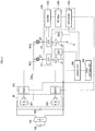
- FIG. 2 is a block view illustrating an example of an induction heating device.
- an induction heating device 1 may include a power supply unit 100, a rectifying unit 150, an inverter unit IV, an inverter driving unit IVD, the first and second working coils WC1 and WC2, the first and second semiconductor switches S1 and S2, the first and second semiconductor switch driving units SD1 and SD2, an over-current protection unit 230, a control unit 250, an input interface 350.
- the power supply unit 100 may output the alternating current power to provide it to the rectifying unit 150, and may be, for example, a commercial power supply.
- the rectifying unit 150 may rectify the alternating current power supplied from the power supply unit 100 to convert a supplied alternating current power to the direct current power.
- a direct current power rectified by the rectifying unit 150 and the direct current link capacitor 200 in FIG. 3 can be supplied to the inverter unit IV.
- the inverter unit IV may perform a switching operation to apply a resonance current to at least one of the first and second working coils WC1 and WC2.
- the inverter unit IV may receive the direct current power from the rectifying unit 150 to perform the switching operation. That is, the inverter unit IV may receive a direct current power that is rectified by the rectifying unit 150 and the ripple is reduced by the direct current link capacitor 200 in FIG. 3 .
- the switching operation can be controlled by the inverter driving unit IVD and it is possible to apply the resonant current to at least one of the first and second working coils WC1 and WC2 through the switching operation. That is, the inverter unit IV can drive a corresponding working coil by providing the resonance current to at least one of the first and second working coils WC1 and WC2, and accordingly, the corresponding working coil performs an induction heating operation.
- the inverter unit IV may include a plurality of switching elements (for example, the first and second switching elements (SV1 and SV2 in FIG. 3 ) to perform the switching operation, and each of the plurality of switching elements may include, for example, an insulated gate bipolar mode transistor (IGBT), but is not limited thereto.
- IGBT insulated gate bipolar mode transistor
- the plurality of switching elements can be turned-on and turned-off alternately by the switching signal received from the inverter driving unit IVD.
- the alternating current of a high frequency (that is, the resonance current) can be generated by the switching operation of the plurality of switching elements, and a generated alternating current of a high frequency can be applied to any one of the first and second working coils WC1 and WC2.
- the inverter driving unit IVD may be controlled by the control unit 250 and may turn on or turn off the switching element provided in the inverter unit IV (i.e., the first and second switching elements SV1 and SV2 in FIG. 3 ).
- the inverter driving unit IVD can receive a pulse signal from the control unit 250, and can generate a switching signal based on a received pulse signal.
- the inverter driving unit IVD can control the switching operation of the switching element provided in the inverter unit IV by providing a generated switching signal to the inverter unit IV.
- the first and second working coils WC1 and WC2 may be connected in parallel with each other.
- first and second working coils WC1 and WC2 may be connected in parallel with each other to form a working coil unit, and may be applied with the resonance current from the inverter unit IV.
- a driving mode of the induction heating device 1 is an induction heating mode
- an eddy current may be generated between the corresponding working coil and a target object, so that the object can be heated.
- a magnetic field may be generated in the corresponding working coil by the alternating current of the high frequency applied from the inverter unit IV to at least one of the first and second working coils WC1 and WC2.
- a current flows also in a coil inside a target object corresponded to the corresponding working coil, and the target object can be charged by the current that flows in the coil inside the target object.
- each working coil can be turned-on or turned-off at the high speed by a corresponding semiconductor switch.
- a flow of the resonance current applied from the inverter unit to the working coil is unblocked or blocked by the semiconductor switch, respectively.
- the first and second semiconductor switches S1 and S2 may be connected to the first and second working coils WC1 and WC2 respectively in order to turn on or turn off the first and second working coils WC1 and WC2, respectively.
- the first semiconductor switch S1 may be connected to the first working coil WC1 to turn on or turn off the first working coil WC1
- the second semiconductor switch S2 may be connected to the second working coil WC2 to turn on or turn off the second working coil WC2.
- the first semiconductor switch S1 may be connected to the first semiconductor switch driving unit SD1 and can be controlled (i.e., turned-on or turned-off) by the first semiconductor switch driving unit SD1.
- the second semiconductor switch S2 may be connected to the second semiconductor switch driving unit SD2 and may be controlled (i.e., turned-on or turned-off) by the second semiconductor switch driving unit SD2.
- the auxiliary power supply may have a single output structure (i.e., an output terminal).
- the auxiliary power supply can supply a power to the first and second semiconductor switches S1 and S2 with a single output.
- the auxiliary power supply can reduce the number of pins required for connection with the first and second semiconductor switches S1 and S2, as compared with other multiple output structures.
- the auxiliary power supply may be designed in a dual output structure (a structure in which each output terminal outputs it by dividing the single output capacity into a capacity of a preset reference capacity or less).
- the auxiliary power supply may include, for example, a Switched mode power supply (SMPS), but is not limited thereto.
- SMPS Switched mode power supply
- the first semiconductor switch driving unit SD1 may be connected to the first semiconductor switch S1 to control a driving of the first semiconductor switch S1.
- the first semiconductor switch driving unit SD1 can turn on or turn off the first semiconductor switch S1 and can be controlled by the control unit 250.
- the second semiconductor switch driving unit SD2 may turn on or turn off the second semiconductor switch S2, and may be controlled by the control unit 250.
- the control unit 250 can control the operation of the inverter driving unit IVD and the first and second semiconductor switch driving units SD1 and SD2, respectively.
- control unit 250 can control the inverter driving unit IVD that turns-on or turns-off the switching element (i.e., the first and second switching elements SV1 and SV2 in FIG. 3 ) provided in the inverter unit IV to indirectly control the switching operation of the inverter unit IV.
- the control unit 250 can indirectly control an operation of the first semiconductor switch S1 by controlling the first semiconductor switch driving unit SD1 and can indirectly control an operation of the second semiconductor switch S2 by controlling the second semiconductor switch driving unit SD2.
- the control unit 250 can generate various pulse signals through a Pulse Width Modulation (PWM) function, and can provide a generated pulse signal to the inverter driving unit IVD.
- PWM Pulse Width Modulation
- a control signal that the control unit 250 provides to the first and second semiconductor switch driving units SD1 and SD2 may also be a form of a pulse signal, and a specific matter thereof will be omitted.
- turning-off the pulse signal may include maintaining the pulse signal at a low level (for example, '0'), or not providing the pulse signal itself.
- the control unit 250 may turn off the pulse signal provided to the inverter driving unit IVD and the semiconductor switch driving unit (for example, the first semiconductor switch driving unit SD1), and thus, a specific matter thereof will be described later.
- the induction heating device 1 may have a wireless power transmission function.
- a technology that supplies a power wirelessly is developed and applied to many electronic devices.
- a battery may be charged by just placing it on a charging pad without connecting a separate charging connector.
- the electronic device to which the wireless power transmission is applied does not require a wire cord or a charging device, such that there may be an advantage in improving portability and reducing size/weight.
- control unit 250 can control the driving mode of the induction heating device 1, i.e., the induction heating mode or the wireless power transmission mode.
- the driving mode of the induction heating device 1 is set to the wireless power transmission mode by the control unit 250, at least one of the first and second working coils WC1 and WC2 is driven to wirelessly transmit the power to the target object.
- the number of working coils driven by the control of the control unit 250 can be determined, and an amount of transmitted power or a heating intensity of the induction heating device 1 can be changed depending on the number of the driven working coils.
- the control unit 250 can control an output intensity of the working coils WC1 and WC2 by adjusting a pulse width of the control signal provided to the semiconductor switches S1 and S2.
- control unit 250 may determine whether the target object is a magnetic body or a non-magnetic body based on the detection value.
- control unit 250 may perform the target object detection function as an example.
- the driving of the induction heating device 1 can be started. Conversely, when the user touches the power supply button for certain time in a state in which the induction heating device 1 is being driven, the driving of the induction heating device 1 may be ended.
- the user can set a driving time of the induction heating device 1 by touching the timer adjustment button (+, -).
- the control unit 250 may terminate the driving of the induction heating device 1 when driving time that the user sets has elapsed.
- the induction heating device 1 can be driven in the wireless power transmission mode.
- control unit 250 can determine the type of the target object, and can grasp the charging mode of the target object based on the received device information.
- control unit 250 can control the frequency of the inverter unit IV by controlling the inverter driving unit IVD according to a confirmed charging mode. For example, in the case of the high speed charging mode, the control unit 250 can adjust the frequency so that a larger magnitude of resonance current is applied to the working coil in accordance with the switching operation of the inverter unit IV.
- the over-current protection unit 230 may be connected to the first and second semiconductor switches S1 and S2.
- the induction heating device 1 can have the above-mentioned feature and configuration.
- the first current transformer CT1 may include a primary coil connected between the first working coil WC1 and the first semiconductor switch S1 and a secondary coil connected to the rectifier 233.
- the primary coil has the larger number of windings than the secondary coil, and thus, the magnitude of the current applied to the primary coil (i.e., the current I2 that flows between the second working coil WC2 and the second semiconductor switch S2) may be greater than the magnitude of the current applied to the secondary coil (i.e., the current provided to the rectifier 233).
- the rectifier 233 may receive a magnitude-converted current from at least one of the first and second current transformers CT1 and CT2 and can rectify a received current. In some implementations, the rectifier 233 may provide a rectified current to the RC filter 236.
- the comparator 239 may receive the noise-reduced current from the RC filter 236 and compare the magnitude of the received current with a preset over-current magnitude to generate an analysis result and determine turning off or not turning off of the inverter driving unit IVD based on the analysis result, and provide the analysis result to a control unit 250.
- the over-current protection unit 230 may continuously observe an occurrence or not of an over-current of the first semiconductor switch S1 by analyzing the current that flows in the first semiconductor switch S1 again.
- the over-current protection unit 230 may simultaneously analyze the current that flows in both the first and second semiconductor switches S1 and S2, and may sequentially analyze each current. Accordingly, the first analysis result indicates that the magnitude of the noise-reduced current received from the RC filter 236 is less than the magnitude of the preset over-current in the state in which the current simultaneously flows in the first and second semiconductor switches S1 and S2, the over-current protection unit 230 may analyze the current I2 that flows in the second semiconductor switch S2, not the first semiconductor switch S1. Alternatively, it is also possible to simultaneously analyze the current that flows in the first and second semiconductor switches S1 and S2.
- control unit 250 may receive the first analysis result from the comparator 239, and turn off the pulse signal provided to the inverter driving unit IVD and the first semiconductor switch driving unit SD1 based on the received first analysis result.
- an example of the over-current protection unit and the control unit of FIG. 3 may reduce the switch stress.
- FIG. 5 and FIG. 6 a characteristic and a configuration of another example of an over-current protection unit 230 will be described in more specifically.
- the first shunt resistor SR1 may be connected between a first semiconductor switch S1 and a ground G.
- the second shunt resistor SR2 may be connected between a second semiconductor switch S2 and a ground G.
- a resistance value of the second shunt resistor SR2 may also be very small.
- the RC filter 236 may receive the rectified voltage from the rectifier 233 and can remove or reduce noise of a received voltage.
- the RC filter 236 may provide a noise-reduced voltage to a comparator 239.
- the "noise-reduced" voltage may mean a noise-removed voltage in which some or all of the noise in a certain frequency range is removed from the rectified voltage from the rectifier 233 by the RC filter 236.
- the comparator 239 may receive the noise-reduced voltage from the RC filter 236, and compare a magnitude of a received voltage with a preset over-voltage magnitude to generate an analysis result, and determined turning off or not turning off of an inverter driving unit IVD based on the analysis result, and provide the analysis result to a control unit 250.
- the comparator 239 may generate the first analysis result, and provide the generated analysis result to the control unit 250.
- the comparator 239 may generate the second analysis result, and provide the generated second analysis result to the control unit 250.
- the over-current protection unit 230 can continuously observe an occurrence or not of an over-current of the first semiconductor switch S1 by analyzing the current I1 that flows in the first semiconductor switch S1 again.
- the over-current protection unit 230 may simultaneously analyze the current that flows in both the first and second semiconductor switches S1 and S2, and may sequentially analyze each current. Accordingly, when the first analysis result indicates that the magnitude of the noise-reduced voltage received from the RC filter 236 is less than the preset over-voltage magnitude in the state in which the current flows in the first and second semiconductor switches S1 and S2 simultaneously, the over-current protection unit 230 may also analyze the current I2 that flows in the second semiconductor switch S2, not the first semiconductor switch S1. Alternatively, the over-current protection unit 230 may also analyze the current that flows in the first and second semiconductor switches S1 and S2 simultaneously.
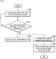
- the comparator 239 may firstly turn off the inverter driving unit IVD to stop a driving of the inverter unit IV, and the supply of the over-current, which was provided to the first semiconductor switch S1, may be stopped. Accordingly, even when the control unit 250 turns-off the pulse signal provided to the inverter driving unit IVD and the first semiconductor switch driving unit SD1, the switch stress applied to the first semiconductor switch S1 is reduced, a voltage spike or a damage according to an increase in a heaving value can be prevented.
- the induction heating device 1 can address a noise problem that can occur in a switching operation of the relays by performing an output control operation on the working coil by using the semiconductor switch instead of a relay, and as a result, it is possible to improve a user satisfaction.
- a use convenience can be improved.
Landscapes
- Physics & Mathematics (AREA)
- Electromagnetism (AREA)
- Inverter Devices (AREA)
Applications Claiming Priority (1)
| Application Number | Priority Date | Filing Date | Title |
|---|---|---|---|
| KR1020180120562A KR102626705B1 (ko) | 2018-10-10 | 2018-10-10 | 스위치 스트레스 저감 구조가 개선된 유도 가열 장치 |
Publications (2)
| Publication Number | Publication Date |
|---|---|
| EP3637954A1 true EP3637954A1 (fr) | 2020-04-15 |
| EP3637954B1 EP3637954B1 (fr) | 2022-08-10 |
Family
ID=66092216
Family Applications (1)
| Application Number | Title | Priority Date | Filing Date |
|---|---|---|---|
| EP19167355.7A Active EP3637954B1 (fr) | 2018-10-10 | 2019-04-04 | Dispositif de chauffage par induction ayant une structure de réduction de contrainte de commutation améliorée |
Country Status (3)
| Country | Link |
|---|---|
| US (1) | US11304267B2 (fr) |
| EP (1) | EP3637954B1 (fr) |
| KR (1) | KR102626705B1 (fr) |
Cited By (1)
| Publication number | Priority date | Publication date | Assignee | Title |
|---|---|---|---|---|
| EP4017215A1 (fr) * | 2020-12-17 | 2022-06-22 | Techrein Co., Ltd | Appareil à portée d'induction pour la détection de récipients |
Families Citing this family (1)
| Publication number | Priority date | Publication date | Assignee | Title |
|---|---|---|---|---|
| US11909226B2 (en) * | 2019-05-21 | 2024-02-20 | General Electric Company | Wireless power transmission apparatus with multiple primary coils and adjacent coil muting |
Citations (5)
| Publication number | Priority date | Publication date | Assignee | Title |
|---|---|---|---|---|
| FR2275105A1 (fr) * | 1974-06-17 | 1976-01-09 | Matsushita Electric Industrial Co Ltd | Appareil de chauffage a induction |
| JP4074206B2 (ja) * | 2003-02-21 | 2008-04-09 | 株式会社ダイヘン | 電磁誘導加熱調理器 |
| CN204014137U (zh) * | 2014-08-07 | 2014-12-10 | 佛山市顺德区美的电热电器制造有限公司 | 具备过流保护功能的烹饪设备 |
| US20150250027A1 (en) * | 2012-10-30 | 2015-09-03 | Koshiro Takano | Induction heating cooker |
| EP3364717A1 (fr) * | 2017-02-20 | 2018-08-22 | Samsung Electronics Co., Ltd. | Appareil de cuisson et son procédé de commande |
Family Cites Families (3)
| Publication number | Priority date | Publication date | Assignee | Title |
|---|---|---|---|---|
| JP2004362796A (ja) * | 2003-06-02 | 2004-12-24 | Matsushita Electric Ind Co Ltd | 電磁調理器 |
| DE102014206458A1 (de) | 2014-04-03 | 2015-10-08 | E.G.O. Elektro-Gerätebau GmbH | Induktionsheizvorrichtung und Induktionskochfeld |
| KR102758304B1 (ko) * | 2017-01-03 | 2025-01-23 | 삼성전자주식회사 | 조리장치, 및 그 제어방법 |
-
2018
- 2018-10-10 KR KR1020180120562A patent/KR102626705B1/ko active Active
-
2019
- 2019-03-14 US US16/353,655 patent/US11304267B2/en active Active
- 2019-04-04 EP EP19167355.7A patent/EP3637954B1/fr active Active
Patent Citations (5)
| Publication number | Priority date | Publication date | Assignee | Title |
|---|---|---|---|---|
| FR2275105A1 (fr) * | 1974-06-17 | 1976-01-09 | Matsushita Electric Industrial Co Ltd | Appareil de chauffage a induction |
| JP4074206B2 (ja) * | 2003-02-21 | 2008-04-09 | 株式会社ダイヘン | 電磁誘導加熱調理器 |
| US20150250027A1 (en) * | 2012-10-30 | 2015-09-03 | Koshiro Takano | Induction heating cooker |
| CN204014137U (zh) * | 2014-08-07 | 2014-12-10 | 佛山市顺德区美的电热电器制造有限公司 | 具备过流保护功能的烹饪设备 |
| EP3364717A1 (fr) * | 2017-02-20 | 2018-08-22 | Samsung Electronics Co., Ltd. | Appareil de cuisson et son procédé de commande |
Cited By (2)
| Publication number | Priority date | Publication date | Assignee | Title |
|---|---|---|---|---|
| EP4017215A1 (fr) * | 2020-12-17 | 2022-06-22 | Techrein Co., Ltd | Appareil à portée d'induction pour la détection de récipients |
| US12520388B2 (en) | 2020-12-17 | 2026-01-06 | Techrein CO., LTD | Inducting range apparatus for detecting container |
Also Published As
| Publication number | Publication date |
|---|---|
| KR102626705B1 (ko) | 2024-01-17 |
| KR20200040528A (ko) | 2020-04-20 |
| US20200120762A1 (en) | 2020-04-16 |
| EP3637954B1 (fr) | 2022-08-10 |
| US11304267B2 (en) | 2022-04-12 |
Similar Documents
| Publication | Publication Date | Title |
|---|---|---|
| EP3678453B1 (fr) | Appareil de transmission d'énergie sans fil et de chauffage par induction à algorithme de commande amélioré | |
| US11533787B2 (en) | Induction heating and wireless power transferring device having improved target object detection algorithm | |
| US11395378B2 (en) | Induction heating device having improved interference noise removal function and power control function | |
| US11064576B2 (en) | Induction heating and wireless power transferring device having improved resonant current detection accuracy | |
| US11064575B2 (en) | Induction heating device having improved target object detection accuracy and induction heating system including the same | |
| US12295085B2 (en) | Induction heating device with improved control algorithm | |
| US11419188B2 (en) | Induction heating and wireless power transmitting apparatus having improved circuit structure | |
| WO2016172916A1 (fr) | Commande du côté émetteur de systèmes de transfert de puissance sans fil sans utiliser d'informations de couplage mutuel ni de rétroaction sans fil | |
| KR102082507B1 (ko) | 제어 알고리즘 및 회로 구조가 개선된 유도 가열 장치 | |
| KR20190043985A (ko) | 대상체 검출 정확도가 개선된 유도 가열 장치 및 이를 포함하는 유도 가열 시스템 | |
| EP3637954B1 (fr) | Dispositif de chauffage par induction ayant une structure de réduction de contrainte de commutation améliorée | |
| KR102040219B1 (ko) | 간섭 소음 제거 및 출력 제어 기능이 개선된 유도 가열 장치 | |
| KR20090005142U (ko) | 유도가열 조리기 | |
| US12476494B2 (en) | Induction heating and wireless power transmitting apparatus having control algorithm | |
| KR20190043984A (ko) | 공진 전류 검출 정확도가 개선된 유도 가열 및 무선 전력 전송 장치 |
Legal Events
| Date | Code | Title | Description |
|---|---|---|---|
| PUAI | Public reference made under article 153(3) epc to a published international application that has entered the european phase |
Free format text: ORIGINAL CODE: 0009012 |
|
| STAA | Information on the status of an ep patent application or granted ep patent |
Free format text: STATUS: THE APPLICATION HAS BEEN PUBLISHED |
|
| STAA | Information on the status of an ep patent application or granted ep patent |
Free format text: STATUS: REQUEST FOR EXAMINATION WAS MADE |
|
| AK | Designated contracting states |
Kind code of ref document: A1 Designated state(s): AL AT BE BG CH CY CZ DE DK EE ES FI FR GB GR HR HU IE IS IT LI LT LU LV MC MK MT NL NO PL PT RO RS SE SI SK SM TR |
|
| AX | Request for extension of the european patent |
Extension state: BA ME |
|
| 17P | Request for examination filed |
Effective date: 20200330 |
|
| RBV | Designated contracting states (corrected) |
Designated state(s): AL AT BE BG CH CY CZ DE DK EE ES FI FR GB GR HR HU IE IS IT LI LT LU LV MC MK MT NL NO PL PT RO RS SE SI SK SM TR |
|
| STAA | Information on the status of an ep patent application or granted ep patent |
Free format text: STATUS: EXAMINATION IS IN PROGRESS |
|
| 17Q | First examination report despatched |
Effective date: 20210210 |
|
| GRAP | Despatch of communication of intention to grant a patent |
Free format text: ORIGINAL CODE: EPIDOSNIGR1 |
|
| STAA | Information on the status of an ep patent application or granted ep patent |
Free format text: STATUS: GRANT OF PATENT IS INTENDED |
|
| INTG | Intention to grant announced |
Effective date: 20220421 |
|
| GRAS | Grant fee paid |
Free format text: ORIGINAL CODE: EPIDOSNIGR3 |
|
| GRAA | (expected) grant |
Free format text: ORIGINAL CODE: 0009210 |
|
| STAA | Information on the status of an ep patent application or granted ep patent |
Free format text: STATUS: THE PATENT HAS BEEN GRANTED |
|
| AK | Designated contracting states |
Kind code of ref document: B1 Designated state(s): AL AT BE BG CH CY CZ DE DK EE ES FI FR GB GR HR HU IE IS IT LI LT LU LV MC MK MT NL NO PL PT RO RS SE SI SK SM TR |
|
| REG | Reference to a national code |
Ref country code: AT Ref legal event code: REF Ref document number: 1511511 Country of ref document: AT Kind code of ref document: T Effective date: 20220815 Ref country code: CH Ref legal event code: EP |
|
| REG | Reference to a national code |
Ref country code: IE Ref legal event code: FG4D |
|
| REG | Reference to a national code |
Ref country code: DE Ref legal event code: R096 Ref document number: 602019017959 Country of ref document: DE |
|
| REG | Reference to a national code |
Ref country code: NL Ref legal event code: MP Effective date: 20220810 |
|
| REG | Reference to a national code |
Ref country code: LT Ref legal event code: MG9D |
|
| PG25 | Lapsed in a contracting state [announced via postgrant information from national office to epo] |
Ref country code: SE Free format text: LAPSE BECAUSE OF FAILURE TO SUBMIT A TRANSLATION OF THE DESCRIPTION OR TO PAY THE FEE WITHIN THE PRESCRIBED TIME-LIMIT Effective date: 20220810 Ref country code: RS Free format text: LAPSE BECAUSE OF FAILURE TO SUBMIT A TRANSLATION OF THE DESCRIPTION OR TO PAY THE FEE WITHIN THE PRESCRIBED TIME-LIMIT Effective date: 20220810 Ref country code: PT Free format text: LAPSE BECAUSE OF FAILURE TO SUBMIT A TRANSLATION OF THE DESCRIPTION OR TO PAY THE FEE WITHIN THE PRESCRIBED TIME-LIMIT Effective date: 20221212 Ref country code: NO Free format text: LAPSE BECAUSE OF FAILURE TO SUBMIT A TRANSLATION OF THE DESCRIPTION OR TO PAY THE FEE WITHIN THE PRESCRIBED TIME-LIMIT Effective date: 20221110 Ref country code: NL Free format text: LAPSE BECAUSE OF FAILURE TO SUBMIT A TRANSLATION OF THE DESCRIPTION OR TO PAY THE FEE WITHIN THE PRESCRIBED TIME-LIMIT Effective date: 20220810 Ref country code: LV Free format text: LAPSE BECAUSE OF FAILURE TO SUBMIT A TRANSLATION OF THE DESCRIPTION OR TO PAY THE FEE WITHIN THE PRESCRIBED TIME-LIMIT Effective date: 20220810 Ref country code: LT Free format text: LAPSE BECAUSE OF FAILURE TO SUBMIT A TRANSLATION OF THE DESCRIPTION OR TO PAY THE FEE WITHIN THE PRESCRIBED TIME-LIMIT Effective date: 20220810 Ref country code: FI Free format text: LAPSE BECAUSE OF FAILURE TO SUBMIT A TRANSLATION OF THE DESCRIPTION OR TO PAY THE FEE WITHIN THE PRESCRIBED TIME-LIMIT Effective date: 20220810 |
|
| REG | Reference to a national code |
Ref country code: AT Ref legal event code: MK05 Ref document number: 1511511 Country of ref document: AT Kind code of ref document: T Effective date: 20220810 |
|
| PG25 | Lapsed in a contracting state [announced via postgrant information from national office to epo] |
Ref country code: PL Free format text: LAPSE BECAUSE OF FAILURE TO SUBMIT A TRANSLATION OF THE DESCRIPTION OR TO PAY THE FEE WITHIN THE PRESCRIBED TIME-LIMIT Effective date: 20220810 Ref country code: IS Free format text: LAPSE BECAUSE OF FAILURE TO SUBMIT A TRANSLATION OF THE DESCRIPTION OR TO PAY THE FEE WITHIN THE PRESCRIBED TIME-LIMIT Effective date: 20221210 Ref country code: HR Free format text: LAPSE BECAUSE OF FAILURE TO SUBMIT A TRANSLATION OF THE DESCRIPTION OR TO PAY THE FEE WITHIN THE PRESCRIBED TIME-LIMIT Effective date: 20220810 Ref country code: GR Free format text: LAPSE BECAUSE OF FAILURE TO SUBMIT A TRANSLATION OF THE DESCRIPTION OR TO PAY THE FEE WITHIN THE PRESCRIBED TIME-LIMIT Effective date: 20221111 |
|
| PG25 | Lapsed in a contracting state [announced via postgrant information from national office to epo] |
Ref country code: SM Free format text: LAPSE BECAUSE OF FAILURE TO SUBMIT A TRANSLATION OF THE DESCRIPTION OR TO PAY THE FEE WITHIN THE PRESCRIBED TIME-LIMIT Effective date: 20220810 Ref country code: RO Free format text: LAPSE BECAUSE OF FAILURE TO SUBMIT A TRANSLATION OF THE DESCRIPTION OR TO PAY THE FEE WITHIN THE PRESCRIBED TIME-LIMIT Effective date: 20220810 Ref country code: ES Free format text: LAPSE BECAUSE OF FAILURE TO SUBMIT A TRANSLATION OF THE DESCRIPTION OR TO PAY THE FEE WITHIN THE PRESCRIBED TIME-LIMIT Effective date: 20220810 Ref country code: DK Free format text: LAPSE BECAUSE OF FAILURE TO SUBMIT A TRANSLATION OF THE DESCRIPTION OR TO PAY THE FEE WITHIN THE PRESCRIBED TIME-LIMIT Effective date: 20220810 Ref country code: CZ Free format text: LAPSE BECAUSE OF FAILURE TO SUBMIT A TRANSLATION OF THE DESCRIPTION OR TO PAY THE FEE WITHIN THE PRESCRIBED TIME-LIMIT Effective date: 20220810 Ref country code: AT Free format text: LAPSE BECAUSE OF FAILURE TO SUBMIT A TRANSLATION OF THE DESCRIPTION OR TO PAY THE FEE WITHIN THE PRESCRIBED TIME-LIMIT Effective date: 20220810 |
|
| REG | Reference to a national code |
Ref country code: DE Ref legal event code: R097 Ref document number: 602019017959 Country of ref document: DE |
|
| PG25 | Lapsed in a contracting state [announced via postgrant information from national office to epo] |
Ref country code: SK Free format text: LAPSE BECAUSE OF FAILURE TO SUBMIT A TRANSLATION OF THE DESCRIPTION OR TO PAY THE FEE WITHIN THE PRESCRIBED TIME-LIMIT Effective date: 20220810 Ref country code: EE Free format text: LAPSE BECAUSE OF FAILURE TO SUBMIT A TRANSLATION OF THE DESCRIPTION OR TO PAY THE FEE WITHIN THE PRESCRIBED TIME-LIMIT Effective date: 20220810 |
|
| PLBE | No opposition filed within time limit |
Free format text: ORIGINAL CODE: 0009261 |
|
| STAA | Information on the status of an ep patent application or granted ep patent |
Free format text: STATUS: NO OPPOSITION FILED WITHIN TIME LIMIT |
|
| PG25 | Lapsed in a contracting state [announced via postgrant information from national office to epo] |
Ref country code: AL Free format text: LAPSE BECAUSE OF FAILURE TO SUBMIT A TRANSLATION OF THE DESCRIPTION OR TO PAY THE FEE WITHIN THE PRESCRIBED TIME-LIMIT Effective date: 20220810 |
|
| 26N | No opposition filed |
Effective date: 20230511 |
|
| PG25 | Lapsed in a contracting state [announced via postgrant information from national office to epo] |
Ref country code: SI Free format text: LAPSE BECAUSE OF FAILURE TO SUBMIT A TRANSLATION OF THE DESCRIPTION OR TO PAY THE FEE WITHIN THE PRESCRIBED TIME-LIMIT Effective date: 20220810 |
|
| REG | Reference to a national code |
Ref country code: CH Ref legal event code: PL |
|
| GBPC | Gb: european patent ceased through non-payment of renewal fee |
Effective date: 20230404 |
|
| PG25 | Lapsed in a contracting state [announced via postgrant information from national office to epo] |
Ref country code: LU Free format text: LAPSE BECAUSE OF NON-PAYMENT OF DUE FEES Effective date: 20230404 |
|
| REG | Reference to a national code |
Ref country code: BE Ref legal event code: MM Effective date: 20230430 |
|
| PG25 | Lapsed in a contracting state [announced via postgrant information from national office to epo] |
Ref country code: MC Free format text: LAPSE BECAUSE OF FAILURE TO SUBMIT A TRANSLATION OF THE DESCRIPTION OR TO PAY THE FEE WITHIN THE PRESCRIBED TIME-LIMIT Effective date: 20220810 |
|
| PG25 | Lapsed in a contracting state [announced via postgrant information from national office to epo] |
Ref country code: GB Free format text: LAPSE BECAUSE OF NON-PAYMENT OF DUE FEES Effective date: 20230404 |
|
| PG25 | Lapsed in a contracting state [announced via postgrant information from national office to epo] |
Ref country code: MC Free format text: LAPSE BECAUSE OF FAILURE TO SUBMIT A TRANSLATION OF THE DESCRIPTION OR TO PAY THE FEE WITHIN THE PRESCRIBED TIME-LIMIT Effective date: 20220810 Ref country code: LI Free format text: LAPSE BECAUSE OF NON-PAYMENT OF DUE FEES Effective date: 20230430 Ref country code: GB Free format text: LAPSE BECAUSE OF NON-PAYMENT OF DUE FEES Effective date: 20230404 Ref country code: FR Free format text: LAPSE BECAUSE OF NON-PAYMENT OF DUE FEES Effective date: 20230430 Ref country code: CH Free format text: LAPSE BECAUSE OF NON-PAYMENT OF DUE FEES Effective date: 20230430 |
|
| REG | Reference to a national code |
Ref country code: IE Ref legal event code: MM4A |
|
| PG25 | Lapsed in a contracting state [announced via postgrant information from national office to epo] |
Ref country code: BE Free format text: LAPSE BECAUSE OF NON-PAYMENT OF DUE FEES Effective date: 20230430 |
|
| PG25 | Lapsed in a contracting state [announced via postgrant information from national office to epo] |
Ref country code: IE Free format text: LAPSE BECAUSE OF NON-PAYMENT OF DUE FEES Effective date: 20230404 |
|
| PG25 | Lapsed in a contracting state [announced via postgrant information from national office to epo] |
Ref country code: IE Free format text: LAPSE BECAUSE OF NON-PAYMENT OF DUE FEES Effective date: 20230404 |
|
| PG25 | Lapsed in a contracting state [announced via postgrant information from national office to epo] |
Ref country code: IT Free format text: LAPSE BECAUSE OF FAILURE TO SUBMIT A TRANSLATION OF THE DESCRIPTION OR TO PAY THE FEE WITHIN THE PRESCRIBED TIME-LIMIT Effective date: 20220810 |
|
| PG25 | Lapsed in a contracting state [announced via postgrant information from national office to epo] |
Ref country code: BG Free format text: LAPSE BECAUSE OF FAILURE TO SUBMIT A TRANSLATION OF THE DESCRIPTION OR TO PAY THE FEE WITHIN THE PRESCRIBED TIME-LIMIT Effective date: 20220810 |
|
| PG25 | Lapsed in a contracting state [announced via postgrant information from national office to epo] |
Ref country code: BG Free format text: LAPSE BECAUSE OF FAILURE TO SUBMIT A TRANSLATION OF THE DESCRIPTION OR TO PAY THE FEE WITHIN THE PRESCRIBED TIME-LIMIT Effective date: 20220810 |
|
| PGFP | Annual fee paid to national office [announced via postgrant information from national office to epo] |
Ref country code: DE Payment date: 20250305 Year of fee payment: 7 |
|
| PG25 | Lapsed in a contracting state [announced via postgrant information from national office to epo] |
Ref country code: CY Free format text: LAPSE BECAUSE OF FAILURE TO SUBMIT A TRANSLATION OF THE DESCRIPTION OR TO PAY THE FEE WITHIN THE PRESCRIBED TIME-LIMIT; INVALID AB INITIO Effective date: 20190404 |
|
| PG25 | Lapsed in a contracting state [announced via postgrant information from national office to epo] |
Ref country code: HU Free format text: LAPSE BECAUSE OF FAILURE TO SUBMIT A TRANSLATION OF THE DESCRIPTION OR TO PAY THE FEE WITHIN THE PRESCRIBED TIME-LIMIT; INVALID AB INITIO Effective date: 20190404 |
|
| PG25 | Lapsed in a contracting state [announced via postgrant information from national office to epo] |
Ref country code: TR Free format text: LAPSE BECAUSE OF FAILURE TO SUBMIT A TRANSLATION OF THE DESCRIPTION OR TO PAY THE FEE WITHIN THE PRESCRIBED TIME-LIMIT Effective date: 20220810 |