EP3640967A1 - Klystron - Google Patents
Klystron Download PDFInfo
- Publication number
- EP3640967A1 EP3640967A1 EP17913844.1A EP17913844A EP3640967A1 EP 3640967 A1 EP3640967 A1 EP 3640967A1 EP 17913844 A EP17913844 A EP 17913844A EP 3640967 A1 EP3640967 A1 EP 3640967A1
- Authority
- EP
- European Patent Office
- Prior art keywords
- cavities
- cavity
- resonant
- electrons
- klystron
- Prior art date
- Legal status (The legal status is an assumption and is not a legal conclusion. Google has not performed a legal analysis and makes no representation as to the accuracy of the status listed.)
- Pending
Links
- 230000008878 coupling Effects 0.000 claims description 5
- 238000010168 coupling process Methods 0.000 claims description 5
- 238000005859 coupling reaction Methods 0.000 claims description 5
- 238000011144 upstream manufacturing Methods 0.000 claims description 3
- 230000003993 interaction Effects 0.000 description 15
- 238000006243 chemical reaction Methods 0.000 description 8
- 239000000470 constituent Substances 0.000 description 6
- 230000000694 effects Effects 0.000 description 5
- RYGMFSIKBFXOCR-UHFFFAOYSA-N Copper Chemical compound [Cu] RYGMFSIKBFXOCR-UHFFFAOYSA-N 0.000 description 1
- 229910052802 copper Inorganic materials 0.000 description 1
- 239000010949 copper Substances 0.000 description 1
- 210000000554 iris Anatomy 0.000 description 1
- 230000004048 modification Effects 0.000 description 1
- 238000012986 modification Methods 0.000 description 1
- 230000001846 repelling effect Effects 0.000 description 1
- 230000007480 spreading Effects 0.000 description 1
- 238000006467 substitution reaction Methods 0.000 description 1
Images


Classifications
-
- H—ELECTRICITY
- H01—ELECTRIC ELEMENTS
- H01J—ELECTRIC DISCHARGE TUBES OR DISCHARGE LAMPS
- H01J23/00—Details of transit-time tubes of the types covered by group H01J25/00
- H01J23/02—Electrodes; Magnetic control means; Screens
- H01J23/08—Focusing arrangements, e.g. for concentrating stream of electrons, for preventing spreading of stream
-
- H—ELECTRICITY
- H01—ELECTRIC ELEMENTS
- H01J—ELECTRIC DISCHARGE TUBES OR DISCHARGE LAMPS
- H01J25/00—Transit-time tubes, e.g. klystrons, travelling-wave tubes, magnetrons
- H01J25/02—Tubes with electron stream modulated in velocity or density in a modulator zone and thereafter giving up energy in an inducing zone, the zones being associated with one or more resonators
- H01J25/10—Klystrons, i.e. tubes having two or more resonators, without reflection of the electron stream, and in which the stream is modulated mainly by velocity in the zone of the input resonator
-
- H—ELECTRICITY
- H01—ELECTRIC ELEMENTS
- H01J—ELECTRIC DISCHARGE TUBES OR DISCHARGE LAMPS
- H01J23/00—Details of transit-time tubes of the types covered by group H01J25/00
- H01J23/02—Electrodes; Magnetic control means; Screens
- H01J23/027—Collectors
-
- H—ELECTRICITY
- H01—ELECTRIC ELEMENTS
- H01J—ELECTRIC DISCHARGE TUBES OR DISCHARGE LAMPS
- H01J23/00—Details of transit-time tubes of the types covered by group H01J25/00
- H01J23/12—Vessels; Containers
-
- H—ELECTRICITY
- H01—ELECTRIC ELEMENTS
- H01J—ELECTRIC DISCHARGE TUBES OR DISCHARGE LAMPS
- H01J23/00—Details of transit-time tubes of the types covered by group H01J25/00
- H01J23/16—Circuit elements, having distributed capacitance and inductance, structurally associated with the tube and interacting with the discharge
- H01J23/18—Resonators
- H01J23/20—Cavity resonators; Adjustment or tuning thereof
-
- H—ELECTRICITY
- H01—ELECTRIC ELEMENTS
- H01J—ELECTRIC DISCHARGE TUBES OR DISCHARGE LAMPS
- H01J23/00—Details of transit-time tubes of the types covered by group H01J25/00
- H01J23/16—Circuit elements, having distributed capacitance and inductance, structurally associated with the tube and interacting with the discharge
- H01J23/18—Resonators
- H01J23/22—Connections between resonators, e.g. strapping for connecting resonators of a magnetron
-
- H—ELECTRICITY
- H01—ELECTRIC ELEMENTS
- H01J—ELECTRIC DISCHARGE TUBES OR DISCHARGE LAMPS
- H01J25/00—Transit-time tubes, e.g. klystrons, travelling-wave tubes, magnetrons
- H01J25/02—Tubes with electron stream modulated in velocity or density in a modulator zone and thereafter giving up energy in an inducing zone, the zones being associated with one or more resonators
- H01J25/10—Klystrons, i.e. tubes having two or more resonators, without reflection of the electron stream, and in which the stream is modulated mainly by velocity in the zone of the input resonator
- H01J25/12—Klystrons, i.e. tubes having two or more resonators, without reflection of the electron stream, and in which the stream is modulated mainly by velocity in the zone of the input resonator with pencil-like electron stream in the axis of the resonators
Definitions
- the present invention relates generally to a klystron.
- a klystron is an electron tube used to amplify high-frequency power, and comprises an electron gun unit that emits electrons, input and output units of high-frequency power, a high-frequency interaction unit, and a collector that captures used electrons.
- the high-frequency interaction unit is composed of a plurality of resonant cavities arranged in the traveling direction of electrons.
- the resonant cavities include an input cavity that inputs high-frequency power, an output cavity that outputs high-frequency power, and a plurality of intermediate cavities between the input cavity and the output cavity.
- the electron gun unit and the high-frequency interaction unit, the plurality of resonant cavities constituting the high-frequency interaction unit, and the high-frequency interaction unit and the collector unit are connected by drift tubes, respectively.
- the electrons emitted from the electron gun unit pass through the input cavity, and are bunched by interacting with a plurality of intermediate cavities ahead of the input cavity.
- the kinetic energy of the bunched electrons is applied to the high frequency input from the input cavity, and the bunched electrons in the output cavity are decelerated to be extracted as high-frequency power amplified to the target output from the output unit.
- a klystron has problems that the bunched electrons tend to spread in the traveling direction since they repel each other due to space charge, and that the electrons cannot be uniformly decelerated by the output cavity and the efficiency of conversion into high-frequency power can hardly be improved since the speed of the electrons is varied.
- Patent Literature 1 JP S55-033718 A
- the problem to be solved by the present invention is to provide a klystron with improved efficiency of conversion to high-frequency power.
- a klystron comprises an electron gun unit that emits electrons, a plurality of resonant cavities including an input cavity, a plurality of intermediate cavities, and an output cavity that are sequentially located along the traveling direction of electrons from the electron gun unit, the plurality of intermediate cavities including a plurality of second harmonic cavities, a collector that captures electrons passing through the plurality of resonant cavities, and a plurality of drift tubes provided between the electron gun unit and the input cavity, between the plurality of resonant cavities, and between the output cavity and the collector.
- a first embodiment will be described hereinafter with reference to FIG. 1 to FIG. 3 .
- FIG. 1 is a cross-sectional view showing a schematic structure of a klystron 10.
- the klystron 10 comprises an electron gun unit A that emits electrons 11.
- the electron gun unit A comprises a cathode 12a that generates electrons 11, an anode 12b that accelerates electrons 11, and the like.
- a high-frequency interaction unit B is provided in front of the electron gun unit A located in the traveling direction of the electrons 11.
- the high-frequency interaction unit B comprises a cylindrical tube container 13 and a plurality of resonant cavities 14 formed in the tube container 13 and arranged along the traveling direction of the electrons 11.
- the high-frequency interaction unit B comprises, for example, ten resonant cavities 14a to 14j.
- a collector 15 that captures the electrons 11 having passed through the high-frequency interaction unit B (resonant cavities 14a to 14j) is provided in front of the high-frequency interaction unit B located in the traveling direction of the electrons 11.
- Drift tubes 16a to 16k are connected between the electron gun unit A and the high-frequency interaction portion B, between the plurality of resonant cavities 14a to 14j, and between the high-frequency interaction portion B and the collector 15, respectively.
- the tube container 13 constituting the resonant cavities 14a to 14j and the drift tubes 16a to 16k is formed of, for example, copper.
- an input unit 17 that inputs the high-frequency power is connected to the resonant cavity 14a located on the electron gun unit A side, of the plurality of resonant cavities 14a to 14j constituting the high-frequency interaction unit B, and an output unit 18 that outputs the high-frequency power is connected to the resonant cavity 14j located on the collector 15 side.
- the input unit 17 is a coaxial line
- the output unit 18 is a waveguide.
- the resonant cavity 14a located on the electron gun unit A side is an input cavity 19
- the resonant cavity 14j located on the collector 15 side is an output cavity 20
- a plurality of resonant cavities 14b to 14i located between the input cavity 19 and the output cavity 20 are intermediate cavities 21b to 21i.
- the drift tube 16a is provided between the electron gun unit A and the input cavity 19.
- the drift tube 16k is provided between the output cavity 20 and the collector 15.
- Each of the drift tubes 16b to 16j is provided between a pair of adjacent resonant cavities of the plurality of resonant cavities 14a to 14j.
- the intermediate cavities 21b to 21i include a plurality of fundamental wave cavities 22b, 22c, 22e, 22f, 22h, and 22i, and a plurality of second harmonic cavities 23d and 23g.
- the plurality of second harmonic cavities 23d and 23g are provided at arbitrary positions in the intermediate cavities 21b to 21i.
- a plurality of fundamental wave cavities 22b and 22c are interposed between the second harmonic cavity 23d on the side close to the electron gun unit A and the input cavity 19
- the plurality of fundamental wave cavities 22h and 22i are interposed between and the second harmonic cavity 23g on the side close to the collector 15 and the output cavity 20
- the plurality of fundamental wave cavities 22e and 22f are interposed between the second harmonic cavities 23d and 23g.
- the number of resonant cavities 14a to 14j is ten
- the number of intermediate cavities 21b to 21i is eight
- the number of second harmonic cavities 23d and 23g is two.
- second harmonic cavities 23d and 23g are provided at every two positions of the intermediate cavities 21b to 21i with respect to the traveling direction of the electrons 11. Therefore, the intermediate cavities 21b, 21c, 21e, 21f, 21h, and 21i are the fundamental wave cavities 22b, 22c, 22e, 22f, 22h, and 22i
- the intermediate cavities 21d and 21g are the second harmonic cavities 23d and 23g.
- FIG. 2 is a cross-sectional view showing a part of the tube container 13 of the klystron 10, showing the second harmonic cavities 23d, 23g, and the like.
- the second harmonic cavities 23d and 23g are formed to be smaller in shape than the fundamental wave cavities 22b, 22c, 22e, 22f, 22h, and 22i that are the intermediate cavities 21b, 21c, 21e, 21f, 21h, and 21i other than the second harmonic cavities 23d and 23g.
- the second harmonic cavities 23d and 23g have a smaller outer diameter OD, a narrower width in the traveling direction of electrons, and a smaller cavity volume than the fundamental wave cavities 22b, 22c, 22e, 22f, 22h, and 22i, and an opening width of the gap (opening) 24 communicating with the interior of the drift tubes 16a to 16k is also formed to be small.
- FIG. 3 is a cross-sectional view showing a part of the tube container 13 of the klystron 10, illustrating the interval between the resonant cavities 14a to 14j.
- FIG. 3 shows the relationship between the resonant cavities 14e and 14f representing the resonant cavities 14a to 14j, but the relationship between the other resonant cavities 14a to 14e and 14f to 14j is the same.
- the resonant cavities 14e and 14f (14a to 14j) have a gap 24 communicating with the interior of the drift tubes 16e to 16g (16b to 16j).
- the distance L between the centers of the gaps 24 of the resonant cavities 14e and 14f (14a to 14j) adjacent via the drift tube 16f (16b to 16j) is the distance between the resonant cavities 14e and 14f (i.e., the distance between a pair of adjacent resonant cavities 14 of the resonant cavities 14a to 14j).
- the distance L is desirably 0.05 to 0.08 times the reduced plasma wavelength representing the wavelength.
- the electrons 11 emitted from the electron gun unit A pass through the resonant cavity 14a (input cavity 19) on the electron gun unit A side having an input unit 17 for high-frequency power, and interacts with the plurality of resonant cavities 14b to 14j (the plurality of intermediate cavities 21b to 21i and the output cavity 20) in front of the resonant cavity 14a and are bunched.
- the bunched electrons 11 are decelerated in the resonant cavity 14j (output cavity 20) on the collector 15 side, and are extracted from the output unit 18 as the high-frequency power amplified to a target output.
- the plurality of resonant cavities 14b to 14j include the plurality of second harmonic cavities 23d and 23g and, the second harmonic generated in the second harmonic cavities 23d and 23g is therefore superimposed on the fundamental wave, and the effect of bunching the electrons 11 is enhanced.
- the bunched electrons repel each other due to space charge and the electrons can easily spread in the traveling direction since the degree of gathering of the electrons in each resonant cavity is large, and the electrons cannot be uniformly decelerated with a resonant cavity (output cavity) connected to the output unit and the efficiency of conversion into high-frequency power can hardly be improved since the speed of electrons is varied.
- the electrons 11 can be gradually bunched by, for example, ten resonant cavities 14a to 14j.
- the total number of the resonant cavities 14a to 14j is desirably ten or more in order to gradually bunch the electrons 11.
- the intermediate cavities 21b to 21i can include a plurality of second harmonic cavities 23d and 23g by using, for example, ten resonant cavities 14a to 14j, and the effect of bunching the electrons 11 can be further enhanced.
- the total length of the klystron 10 can be shortened by using the plurality of second harmonic cavities 23d and 23g.
- the plurality of intermediate cavities 21b to 21i are arranged along the traveling direction of the electrons 11. Two or more intermediate cavities 21 are interposed between the second harmonic cavity 23 on the upstream side and the second harmonic cavity 23 on the downstream side, in the traveling direction of the electrons 11. Of the plurality of intermediate cavities 21b to 21i, the plurality of intermediate cavities 21 (fundamental wave cavities 22) other than the plurality of second harmonic cavities 23 include the two or more intermediate cavities 21.
- the plurality of second harmonic cavities 23d and 23g are provided at positions where the plurality of intermediate cavities 21e and 21f are provided between the second harmonic cavity 23d on the upstream side and the second harmonic cavity 23g on the downstream side, in the traveling direction of the electron 11, of the positions of the plurality of intermediate cavities 21b to 21i.
- the effect of bunching the electrons 11 can be further enhanced.
- the plurality of second harmonic cavities 23d and 23g can be arranged at equal intervals in the plurality of intermediate cavities 21b to 21i, and the effect of bunching the electrons 11 can be further enhanced.
- the diameter (inner diameter) D of the drift tubes 16d, 16e, 16g, and 16h adjacent to the second harmonic cavities 23d and 23g is desirably set to half or less of diameter (inner diameter) at which the electromagnetic wave of TE11 mode of the second harmonic is a cutoff frequency.
- the distance L between the centers of the gaps 24 of the resonant cavities 14a to 14j adjacent via the drift tubes 16b to 16j is set to 0.05 to 0.08 times the reduced plasma wavelength representing the wavelength thereof and the arrangement of the resonant cavities 14a to 14j can be thereby optimized.
- the second harmonic cavity 23 It is arbitrarily determined which of the resonant cavities 14a to 14j is used as the second harmonic cavity 23, and three or more second harmonic cavities 23 may be used.
- the plurality of intermediate cavities 21 include three or more second harmonic cavities 23, two or more intermediate cavities 21 (fundamental wave cavities 22) are desirably interposed between a pair of adjacent second harmonic cavities 23.
- a klystron 10 of the second embodiment will be described with reference to FIG. 4 .
- the same constituent elements as those of the first embodiment will be denoted by the same referential numerals, and descriptions of the constituent elements and the advantages will be omitted.
- FIG. 4 is a cross-sectional view showing a tube container 13 and a collector 15 of the klystron 10 of the second embodiment, illustrating diameters of drift tubes 16h to 16k.
- the total number of the resonant cavities 14a to 14j is referred to as n
- D8 ⁇ D9 ⁇ D10 ⁇ Dc the diameters of the drift tubes 16h to 16k
- the bunched electrons 11 can be gradually expanded in the diameter direction of the drift tubes 16h to 16k and the electrons 11 can be prevented from spreading in the traveling direction by repelling caused by the space charge, by using the drift tubes 16h to 16k that satisfy formula (1), and the efficiency of conversion into high-frequency power can be thereby easily improved.
- Gradually increasing the diameter of the drift tube 16 toward the side closer to the collector 15 is not limited to the drift tubes 16h to 16k located on the side closer to the collector 15, but any number of drift tubes of the drift tubes 16a to 16k may be gradually widened toward the collector 15.
- a klystron 10 of a third embodiment will be described with reference to FIG. 5 .
- the same constituent elements as those of each embodiment will be denoted by the same referential numerals, and descriptions of the constituent elements and the advantages will be omitted.
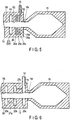
- FIG. 5 is a cross-sectional view showing a tube container 13 and a collector 15 of a klystron 10 of the third embodiment, and shows cavity cells 25a to 25c and the like.
- the resonant cavity 14j that is the output cavity 20 has three or more cavity cells 25.
- the output cavity 20 has three cavity cells 25a to 25c.
- the respective cavity cells 25a to 25c are electrically coupled by irises 26a and 26b provided along the tube axis of the klystron 10.
- the electrical coupling between the resonant cavity 14j and the electrons 11 can be enhanced by using the cavity cells 25a to 25c that are electrically coupled to each other as the resonant cavity 14j, the efficiency of conversion into high-frequency power can easily be improved.
- a klystron 10 of a fourth embodiment will be described with reference to FIG. 6 .
- the same constituent elements as those of each of the embodiments will be denoted by the same referential numerals, and descriptions of the constituent elements and the advantages will be omitted.
- FIG. 6 is a cross-sectional view showing a tube container 13 and a collector 15 of the klystron 10 of the fourth embodiment, and shows cavity cells 25a to 25c and the like.
- the cavity cells 25a to 25c are electrically coupled by coupling holes 27a and 27b provided on the wall surfaces of the cavity cells 25a to 25c.
- the shapes of the coupling holes 27a and 27b are arbitrarily determined.
- the cavity cells 25a to 25c electrically coupled to each other can be used as the resonant cavity 14j (output cavity 20). In this case, too, since the electrical coupling between the resonant cavity 14j and the electrons 11 can be enhanced, the efficiency of conversion into high-frequency power can easily be improved.
- the klystron 10 wherein spread of the bunched electrons 11 in the traveling direction is suppressed by the resonant cavities 14a to 14j, the speed is made uniform, and the efficiency of conversion into high-frequency power is thereby improved, can be provided.
Landscapes
- Microwave Tubes (AREA)
Applications Claiming Priority (2)
| Application Number | Priority Date | Filing Date | Title |
|---|---|---|---|
| JP2017115927A JP7011370B2 (ja) | 2017-06-13 | 2017-06-13 | クライストロン |
| PCT/JP2017/046311 WO2018230018A1 (ja) | 2017-06-13 | 2017-12-25 | クライストロン |
Publications (2)
| Publication Number | Publication Date |
|---|---|
| EP3640967A1 true EP3640967A1 (de) | 2020-04-22 |
| EP3640967A4 EP3640967A4 (de) | 2021-06-23 |
Family
ID=64660241
Family Applications (1)
| Application Number | Title | Priority Date | Filing Date |
|---|---|---|---|
| EP17913844.1A Pending EP3640967A4 (de) | 2017-06-13 | 2017-12-25 | Klystron |
Country Status (6)
| Country | Link |
|---|---|
| US (1) | US20200118782A1 (de) |
| EP (1) | EP3640967A4 (de) |
| JP (1) | JP7011370B2 (de) |
| KR (1) | KR20200009050A (de) |
| CN (1) | CN110753988A (de) |
| WO (1) | WO2018230018A1 (de) |
Families Citing this family (5)
| Publication number | Priority date | Publication date | Assignee | Title |
|---|---|---|---|---|
| CN111785598B (zh) * | 2020-07-23 | 2023-08-08 | 中国舰船研究设计中心 | 一种间隙宽度渐变的分布式输出谐振腔 |
| JP7635095B2 (ja) * | 2021-08-18 | 2025-02-25 | キヤノン電子管デバイス株式会社 | クライストロン |
| CN113725053B (zh) * | 2021-09-02 | 2024-03-26 | 中国科学院空天信息创新研究院 | 平面级联速调管 |
| CN115866870B (zh) * | 2022-06-17 | 2025-08-22 | 上海科技大学 | 光阴极超导射频电子枪 |
| CN118553576B (zh) * | 2024-05-15 | 2026-04-17 | 电子科技大学 | 一种基于混合模式谐振腔实现高效率紧凑型速调管的方法 |
Family Cites Families (13)
| Publication number | Priority date | Publication date | Assignee | Title |
|---|---|---|---|---|
| US2963605A (en) * | 1954-11-04 | 1960-12-06 | Varian Associates | Ion draining structures |
| US3548246A (en) * | 1966-09-29 | 1970-12-15 | Gen Electric | Biconical log periodic amplifier |
| FR2153585A5 (de) * | 1971-09-16 | 1973-05-04 | Thomson Csf | |
| JPS5010552A (de) * | 1973-05-24 | 1975-02-03 | ||
| JPS592137B2 (ja) | 1978-09-01 | 1984-01-17 | 株式会社東芝 | 直進形クライストロン |
| US4931695A (en) * | 1988-06-02 | 1990-06-05 | Litton Systems, Inc. | High performance extended interaction output circuit |
| JP3075741B2 (ja) * | 1990-11-22 | 2000-08-14 | 株式会社東芝 | 多空胴直進形クライストロン |
| GB9724960D0 (en) * | 1997-11-27 | 1998-01-28 | Eev Ltd | Electron beam tubes |
| FR2786022B1 (fr) * | 1998-11-18 | 2001-03-09 | Thomson Tubes Electroniques | Tube electronique multifaisceau a interception des electrons minimisee |
| JP4533588B2 (ja) * | 2003-02-19 | 2010-09-01 | 株式会社東芝 | クライストロン装置 |
| JP5377234B2 (ja) * | 2009-11-05 | 2013-12-25 | 株式会社東芝 | クライストロン装置 |
| CN104157538A (zh) * | 2014-08-19 | 2014-11-19 | 中国科学院电子学研究所 | 托卡马克装置用高功率连续波速调管 |
| US9697978B2 (en) * | 2015-06-17 | 2017-07-04 | The Board Of Trustees Of The Leland Stanford Junior University | Multi-frequency klystron designed for high efficiency |
-
2017
- 2017-06-13 JP JP2017115927A patent/JP7011370B2/ja active Active
- 2017-12-25 KR KR1020197037243A patent/KR20200009050A/ko not_active Ceased
- 2017-12-25 CN CN201780091971.3A patent/CN110753988A/zh active Pending
- 2017-12-25 EP EP17913844.1A patent/EP3640967A4/de active Pending
- 2017-12-25 WO PCT/JP2017/046311 patent/WO2018230018A1/ja not_active Ceased
-
2019
- 2019-12-13 US US16/713,123 patent/US20200118782A1/en not_active Abandoned
Also Published As
| Publication number | Publication date |
|---|---|
| CN110753988A (zh) | 2020-02-04 |
| US20200118782A1 (en) | 2020-04-16 |
| JP2019003766A (ja) | 2019-01-10 |
| EP3640967A4 (de) | 2021-06-23 |
| WO2018230018A1 (ja) | 2018-12-20 |
| JP7011370B2 (ja) | 2022-01-26 |
| KR20200009050A (ko) | 2020-01-29 |
Similar Documents
| Publication | Publication Date | Title |
|---|---|---|
| EP3640967A1 (de) | Klystron | |
| KR101723876B1 (ko) | 접혀진 형상의 도파관 및 이를 포함하는 진행파관기 | |
| CN106128911B (zh) | 一种用于行波管的矩形慢波线 | |
| CN101651074A (zh) | 一种脊加载曲折波导慢波线 | |
| CN102509686B (zh) | 回旋行波管用宽带多波导输出装置 | |
| WO2011022643A2 (en) | Crossed field device | |
| CN102324363A (zh) | 一种脊加载曲折矩形槽波导慢波线 | |
| CN101770919B (zh) | 一种用于行波管的慢波线 | |
| EP3392899B1 (de) | Langsamwellenschaltung und wanderfeldröhre | |
| CN202855699U (zh) | 一种曲折波导慢波线 | |
| CN102013375B (zh) | 一种适用于卷绕双梳齿慢波结构的能量耦合装置 | |
| CN110112046A (zh) | 一种半矩形环螺旋线慢波结构 | |
| CN102915898A (zh) | 一种曲折波导慢波线 | |
| US3243735A (en) | Delay line for travelling wave tubes | |
| JP4991266B2 (ja) | マルチビームクライストロン | |
| CN119297061A (zh) | 加载二次谐波腔的低磁场高效率同轴相对论速调管振荡器 | |
| JP7032222B2 (ja) | クライストロン | |
| CN202150438U (zh) | 一种脊加载曲折矩形槽波导慢波线 | |
| JP5016904B2 (ja) | マルチビームクライストロン | |
| US3400297A (en) | Traveling-wave type electron tube utilizing interaction between beam and te20 waveguide mode | |
| Shu et al. | High-order overmoded based multiple sheet electron beam devices | |
| CN201663142U (zh) | 一种用于行波管的慢波线 | |
| WO2015063519A1 (en) | Waveguide | |
| JP5377234B2 (ja) | クライストロン装置 | |
| RU135203U1 (ru) | Импульсный двухкаскадный моноблочный усилитель мощности свч на амплитронах |
Legal Events
| Date | Code | Title | Description |
|---|---|---|---|
| STAA | Information on the status of an ep patent application or granted ep patent |
Free format text: STATUS: THE INTERNATIONAL PUBLICATION HAS BEEN MADE |
|
| PUAI | Public reference made under article 153(3) epc to a published international application that has entered the european phase |
Free format text: ORIGINAL CODE: 0009012 |
|
| STAA | Information on the status of an ep patent application or granted ep patent |
Free format text: STATUS: REQUEST FOR EXAMINATION WAS MADE |
|
| 17P | Request for examination filed |
Effective date: 20191213 |
|
| AK | Designated contracting states |
Kind code of ref document: A1 Designated state(s): AL AT BE BG CH CY CZ DE DK EE ES FI FR GB GR HR HU IE IS IT LI LT LU LV MC MK MT NL NO PL PT RO RS SE SI SK SM TR |
|
| AX | Request for extension of the european patent |
Extension state: BA ME |
|
| DAV | Request for validation of the european patent (deleted) | ||
| DAX | Request for extension of the european patent (deleted) | ||
| RIC1 | Information provided on ipc code assigned before grant |
Ipc: H01J 23/22 20060101ALI20210205BHEP Ipc: H01J 23/12 20060101ALI20210205BHEP Ipc: H01J 23/08 20060101ALI20210205BHEP Ipc: H01J 25/12 20060101ALI20210205BHEP Ipc: H01J 23/20 20060101AFI20210205BHEP |
|
| A4 | Supplementary search report drawn up and despatched |
Effective date: 20210525 |
|
| RIC1 | Information provided on ipc code assigned before grant |
Ipc: H01J 23/20 20060101AFI20210518BHEP Ipc: H01J 23/08 20060101ALI20210518BHEP Ipc: H01J 23/12 20060101ALI20210518BHEP Ipc: H01J 23/22 20060101ALI20210518BHEP Ipc: H01J 25/12 20060101ALI20210518BHEP |