EP3640982B1 - Amplicateur doherty basé sur une carte de circuit imprimé avec des éléments de réseau d'adaptation d'impédance intégrés dans la carte de circuit imprimé - Google Patents
Amplicateur doherty basé sur une carte de circuit imprimé avec des éléments de réseau d'adaptation d'impédance intégrés dans la carte de circuit imprimé Download PDFInfo
- Publication number
- EP3640982B1 EP3640982B1 EP19207270.0A EP19207270A EP3640982B1 EP 3640982 B1 EP3640982 B1 EP 3640982B1 EP 19207270 A EP19207270 A EP 19207270A EP 3640982 B1 EP3640982 B1 EP 3640982B1
- Authority
- EP
- European Patent Office
- Prior art keywords
- layer
- embedded
- circuit board
- doherty amplifier
- composite fiber
- Prior art date
- Legal status (The legal status is an assumption and is not a legal conclusion. Google has not performed a legal analysis and makes no representation as to the accuracy of the status listed.)
- Active
Links
Images




Classifications
-
- H—ELECTRICITY
- H05—ELECTRIC TECHNIQUES NOT OTHERWISE PROVIDED FOR
- H05K—PRINTED CIRCUITS; CASINGS OR CONSTRUCTIONAL DETAILS OF ELECTRIC APPARATUS; MANUFACTURE OF ASSEMBLAGES OF ELECTRICAL COMPONENTS
- H05K1/00—Printed circuits
- H05K1/02—Details
- H05K1/0213—Electrical arrangements not otherwise provided for
-
- H—ELECTRICITY
- H05—ELECTRIC TECHNIQUES NOT OTHERWISE PROVIDED FOR
- H05K—PRINTED CIRCUITS; CASINGS OR CONSTRUCTIONAL DETAILS OF ELECTRIC APPARATUS; MANUFACTURE OF ASSEMBLAGES OF ELECTRICAL COMPONENTS
- H05K1/00—Printed circuits
- H05K1/02—Details
- H05K1/0213—Electrical arrangements not otherwise provided for
- H05K1/0237—High frequency adaptations
- H05K1/024—Dielectric details, e.g. changing the dielectric material around a transmission line
-
- H—ELECTRICITY
- H05—ELECTRIC TECHNIQUES NOT OTHERWISE PROVIDED FOR
- H05K—PRINTED CIRCUITS; CASINGS OR CONSTRUCTIONAL DETAILS OF ELECTRIC APPARATUS; MANUFACTURE OF ASSEMBLAGES OF ELECTRICAL COMPONENTS
- H05K1/00—Printed circuits
- H05K1/02—Details
- H05K1/0213—Electrical arrangements not otherwise provided for
- H05K1/0237—High frequency adaptations
- H05K1/0243—Printed circuits associated with mounted high frequency components
-
- H—ELECTRICITY
- H05—ELECTRIC TECHNIQUES NOT OTHERWISE PROVIDED FOR
- H05K—PRINTED CIRCUITS; CASINGS OR CONSTRUCTIONAL DETAILS OF ELECTRIC APPARATUS; MANUFACTURE OF ASSEMBLAGES OF ELECTRICAL COMPONENTS
- H05K1/00—Printed circuits
- H05K1/02—Details
- H05K1/0213—Electrical arrangements not otherwise provided for
- H05K1/0237—High frequency adaptations
- H05K1/025—Impedance arrangements, e.g. impedance matching, reduction of parasitic impedance
-
- H—ELECTRICITY
- H05—ELECTRIC TECHNIQUES NOT OTHERWISE PROVIDED FOR
- H05K—PRINTED CIRCUITS; CASINGS OR CONSTRUCTIONAL DETAILS OF ELECTRIC APPARATUS; MANUFACTURE OF ASSEMBLAGES OF ELECTRICAL COMPONENTS
- H05K1/00—Printed circuits
- H05K1/02—Details
- H05K1/0296—Conductive pattern lay-out details not covered by sub groups H05K1/02 - H05K1/0295
- H05K1/0298—Multilayer circuits
-
- H—ELECTRICITY
- H05—ELECTRIC TECHNIQUES NOT OTHERWISE PROVIDED FOR
- H05K—PRINTED CIRCUITS; CASINGS OR CONSTRUCTIONAL DETAILS OF ELECTRIC APPARATUS; MANUFACTURE OF ASSEMBLAGES OF ELECTRICAL COMPONENTS
- H05K1/00—Printed circuits
- H05K1/02—Details
- H05K1/03—Use of materials for the substrate
- H05K1/0313—Organic insulating material
- H05K1/0353—Organic insulating material consisting of two or more materials, e.g. two or more polymers, polymer + filler, + reinforcement
- H05K1/0366—Organic insulating material consisting of two or more materials, e.g. two or more polymers, polymer + filler, + reinforcement reinforced, e.g. by fibres, fabrics
-
- H—ELECTRICITY
- H05—ELECTRIC TECHNIQUES NOT OTHERWISE PROVIDED FOR
- H05K—PRINTED CIRCUITS; CASINGS OR CONSTRUCTIONAL DETAILS OF ELECTRIC APPARATUS; MANUFACTURE OF ASSEMBLAGES OF ELECTRICAL COMPONENTS
- H05K1/00—Printed circuits
- H05K1/02—Details
- H05K1/11—Printed elements for providing electric connections to or between printed circuits
- H05K1/111—Pads for surface mounting, e.g. lay-out
-
- H—ELECTRICITY
- H05—ELECTRIC TECHNIQUES NOT OTHERWISE PROVIDED FOR
- H05K—PRINTED CIRCUITS; CASINGS OR CONSTRUCTIONAL DETAILS OF ELECTRIC APPARATUS; MANUFACTURE OF ASSEMBLAGES OF ELECTRICAL COMPONENTS
- H05K1/00—Printed circuits
- H05K1/02—Details
- H05K1/11—Printed elements for providing electric connections to or between printed circuits
- H05K1/115—Via connections; Lands around holes or via connections
-
- H—ELECTRICITY
- H05—ELECTRIC TECHNIQUES NOT OTHERWISE PROVIDED FOR
- H05K—PRINTED CIRCUITS; CASINGS OR CONSTRUCTIONAL DETAILS OF ELECTRIC APPARATUS; MANUFACTURE OF ASSEMBLAGES OF ELECTRICAL COMPONENTS
- H05K1/00—Printed circuits
- H05K1/16—Printed circuits incorporating printed electric components, e.g. printed resistors, capacitors or inductors
- H05K1/162—Printed circuits incorporating printed electric components, e.g. printed resistors, capacitors or inductors incorporating printed capacitors
-
- H—ELECTRICITY
- H05—ELECTRIC TECHNIQUES NOT OTHERWISE PROVIDED FOR
- H05K—PRINTED CIRCUITS; CASINGS OR CONSTRUCTIONAL DETAILS OF ELECTRIC APPARATUS; MANUFACTURE OF ASSEMBLAGES OF ELECTRICAL COMPONENTS
- H05K1/00—Printed circuits
- H05K1/18—Printed circuits structurally associated with non-printed electric components
- H05K1/182—Printed circuits structurally associated with non-printed electric components associated with components mounted in printed circuit boards [PCB], e.g. insert-mounted components [IMC]
- H05K1/183—Printed circuits structurally associated with non-printed electric components associated with components mounted in printed circuit boards [PCB], e.g. insert-mounted components [IMC] associated with components mounted in and supported by recessed areas of the PCBs
-
- H—ELECTRICITY
- H10—SEMICONDUCTOR DEVICES; ELECTRIC SOLID-STATE DEVICES NOT OTHERWISE PROVIDED FOR
- H10W—GENERIC PACKAGES, INTERCONNECTIONS, CONNECTORS OR OTHER CONSTRUCTIONAL DETAILS OF DEVICES COVERED BY CLASS H10
- H10W20/00—Interconnections in chips, wafers or substrates
- H10W20/40—Interconnections external to wafers or substrates, e.g. back-end-of-line [BEOL] metallisations or vias connecting to gate electrodes
- H10W20/45—Interconnections external to wafers or substrates, e.g. back-end-of-line [BEOL] metallisations or vias connecting to gate electrodes characterised by their insulating parts
- H10W20/48—Insulating materials thereof
-
- H—ELECTRICITY
- H10—SEMICONDUCTOR DEVICES; ELECTRIC SOLID-STATE DEVICES NOT OTHERWISE PROVIDED FOR
- H10W—GENERIC PACKAGES, INTERCONNECTIONS, CONNECTORS OR OTHER CONSTRUCTIONAL DETAILS OF DEVICES COVERED BY CLASS H10
- H10W20/00—Interconnections in chips, wafers or substrates
- H10W20/40—Interconnections external to wafers or substrates, e.g. back-end-of-line [BEOL] metallisations or vias connecting to gate electrodes
- H10W20/49—Adaptable interconnections, e.g. fuses or antifuses
-
- H—ELECTRICITY
- H10—SEMICONDUCTOR DEVICES; ELECTRIC SOLID-STATE DEVICES NOT OTHERWISE PROVIDED FOR
- H10W—GENERIC PACKAGES, INTERCONNECTIONS, CONNECTORS OR OTHER CONSTRUCTIONAL DETAILS OF DEVICES COVERED BY CLASS H10
- H10W44/00—Electrical arrangements for controlling or matching impedance
- H10W44/20—Electrical arrangements for controlling or matching impedance at high-frequency [HF] or radio frequency [RF]
-
- H—ELECTRICITY
- H10—SEMICONDUCTOR DEVICES; ELECTRIC SOLID-STATE DEVICES NOT OTHERWISE PROVIDED FOR
- H10W—GENERIC PACKAGES, INTERCONNECTIONS, CONNECTORS OR OTHER CONSTRUCTIONAL DETAILS OF DEVICES COVERED BY CLASS H10
- H10W70/00—Package substrates; Interposers; Redistribution layers [RDL]
- H10W70/60—Insulating or insulated package substrates; Interposers; Redistribution layers
-
- H—ELECTRICITY
- H10—SEMICONDUCTOR DEVICES; ELECTRIC SOLID-STATE DEVICES NOT OTHERWISE PROVIDED FOR
- H10W—GENERIC PACKAGES, INTERCONNECTIONS, CONNECTORS OR OTHER CONSTRUCTIONAL DETAILS OF DEVICES COVERED BY CLASS H10
- H10W70/00—Package substrates; Interposers; Redistribution layers [RDL]
- H10W70/60—Insulating or insulated package substrates; Interposers; Redistribution layers
- H10W70/62—Insulating or insulated package substrates; Interposers; Redistribution layers characterised by their interconnections
- H10W70/63—Vias, e.g. via plugs
- H10W70/635—Through-vias
-
- H—ELECTRICITY
- H10—SEMICONDUCTOR DEVICES; ELECTRIC SOLID-STATE DEVICES NOT OTHERWISE PROVIDED FOR
- H10W—GENERIC PACKAGES, INTERCONNECTIONS, CONNECTORS OR OTHER CONSTRUCTIONAL DETAILS OF DEVICES COVERED BY CLASS H10
- H10W70/00—Package substrates; Interposers; Redistribution layers [RDL]
- H10W70/60—Insulating or insulated package substrates; Interposers; Redistribution layers
- H10W70/62—Insulating or insulated package substrates; Interposers; Redistribution layers characterised by their interconnections
- H10W70/65—Shapes or dispositions of interconnections
- H10W70/658—Shapes or dispositions of interconnections for devices provided for in groups H10D8/00 - H10D48/00
-
- H—ELECTRICITY
- H10—SEMICONDUCTOR DEVICES; ELECTRIC SOLID-STATE DEVICES NOT OTHERWISE PROVIDED FOR
- H10W—GENERIC PACKAGES, INTERCONNECTIONS, CONNECTORS OR OTHER CONSTRUCTIONAL DETAILS OF DEVICES COVERED BY CLASS H10
- H10W70/00—Package substrates; Interposers; Redistribution layers [RDL]
- H10W70/60—Insulating or insulated package substrates; Interposers; Redistribution layers
- H10W70/67—Insulating or insulated package substrates; Interposers; Redistribution layers characterised by their insulating layers or insulating parts
- H10W70/68—Shapes or dispositions thereof
-
- H—ELECTRICITY
- H10—SEMICONDUCTOR DEVICES; ELECTRIC SOLID-STATE DEVICES NOT OTHERWISE PROVIDED FOR
- H10W—GENERIC PACKAGES, INTERCONNECTIONS, CONNECTORS OR OTHER CONSTRUCTIONAL DETAILS OF DEVICES COVERED BY CLASS H10
- H10W70/00—Package substrates; Interposers; Redistribution layers [RDL]
- H10W70/60—Insulating or insulated package substrates; Interposers; Redistribution layers
- H10W70/67—Insulating or insulated package substrates; Interposers; Redistribution layers characterised by their insulating layers or insulating parts
- H10W70/68—Shapes or dispositions thereof
- H10W70/685—Shapes or dispositions thereof comprising multiple insulating layers
-
- H—ELECTRICITY
- H10—SEMICONDUCTOR DEVICES; ELECTRIC SOLID-STATE DEVICES NOT OTHERWISE PROVIDED FOR
- H10W—GENERIC PACKAGES, INTERCONNECTIONS, CONNECTORS OR OTHER CONSTRUCTIONAL DETAILS OF DEVICES COVERED BY CLASS H10
- H10W72/00—Interconnections or connectors in packages
- H10W72/90—Bond pads, in general
-
- H—ELECTRICITY
- H05—ELECTRIC TECHNIQUES NOT OTHERWISE PROVIDED FOR
- H05K—PRINTED CIRCUITS; CASINGS OR CONSTRUCTIONAL DETAILS OF ELECTRIC APPARATUS; MANUFACTURE OF ASSEMBLAGES OF ELECTRICAL COMPONENTS
- H05K1/00—Printed circuits
- H05K1/02—Details
- H05K1/0213—Electrical arrangements not otherwise provided for
- H05K1/0216—Reduction of cross-talk, noise or electromagnetic interference
- H05K1/023—Reduction of cross-talk, noise or electromagnetic interference using auxiliary mounted passive components or auxiliary substances
- H05K1/0231—Capacitors or dielectric substances
-
- H—ELECTRICITY
- H05—ELECTRIC TECHNIQUES NOT OTHERWISE PROVIDED FOR
- H05K—PRINTED CIRCUITS; CASINGS OR CONSTRUCTIONAL DETAILS OF ELECTRIC APPARATUS; MANUFACTURE OF ASSEMBLAGES OF ELECTRICAL COMPONENTS
- H05K1/00—Printed circuits
- H05K1/02—Details
- H05K1/14—Structural association of two or more printed circuits
- H05K1/144—Stacked arrangements of planar printed circuit boards
-
- H—ELECTRICITY
- H05—ELECTRIC TECHNIQUES NOT OTHERWISE PROVIDED FOR
- H05K—PRINTED CIRCUITS; CASINGS OR CONSTRUCTIONAL DETAILS OF ELECTRIC APPARATUS; MANUFACTURE OF ASSEMBLAGES OF ELECTRICAL COMPONENTS
- H05K2201/00—Indexing scheme relating to printed circuits covered by H05K1/00
- H05K2201/10—Details of components or other objects attached to or integrated in a printed circuit board
- H05K2201/10007—Types of components
- H05K2201/10015—Non-printed capacitor
-
- H—ELECTRICITY
- H05—ELECTRIC TECHNIQUES NOT OTHERWISE PROVIDED FOR
- H05K—PRINTED CIRCUITS; CASINGS OR CONSTRUCTIONAL DETAILS OF ELECTRIC APPARATUS; MANUFACTURE OF ASSEMBLAGES OF ELECTRICAL COMPONENTS
- H05K2201/00—Indexing scheme relating to printed circuits covered by H05K1/00
- H05K2201/10—Details of components or other objects attached to or integrated in a printed circuit board
- H05K2201/10007—Types of components
- H05K2201/1003—Non-printed inductor
-
- H—ELECTRICITY
- H05—ELECTRIC TECHNIQUES NOT OTHERWISE PROVIDED FOR
- H05K—PRINTED CIRCUITS; CASINGS OR CONSTRUCTIONAL DETAILS OF ELECTRIC APPARATUS; MANUFACTURE OF ASSEMBLAGES OF ELECTRICAL COMPONENTS
- H05K2201/00—Indexing scheme relating to printed circuits covered by H05K1/00
- H05K2201/10—Details of components or other objects attached to or integrated in a printed circuit board
- H05K2201/10007—Types of components
- H05K2201/10166—Transistor
-
- H—ELECTRICITY
- H05—ELECTRIC TECHNIQUES NOT OTHERWISE PROVIDED FOR
- H05K—PRINTED CIRCUITS; CASINGS OR CONSTRUCTIONAL DETAILS OF ELECTRIC APPARATUS; MANUFACTURE OF ASSEMBLAGES OF ELECTRICAL COMPONENTS
- H05K2203/00—Indexing scheme relating to apparatus or processes for manufacturing printed circuits covered by H05K3/00
- H05K2203/04—Soldering or other types of metallurgic bonding
- H05K2203/049—Wire bonding
-
- H—ELECTRICITY
- H05—ELECTRIC TECHNIQUES NOT OTHERWISE PROVIDED FOR
- H05K—PRINTED CIRCUITS; CASINGS OR CONSTRUCTIONAL DETAILS OF ELECTRIC APPARATUS; MANUFACTURE OF ASSEMBLAGES OF ELECTRICAL COMPONENTS
- H05K3/00—Apparatus or processes for manufacturing printed circuits
- H05K3/40—Forming printed elements for providing electric connections to or between printed circuits
- H05K3/42—Plated through-holes or plated via connections
- H05K3/421—Blind plated via connections
-
- H—ELECTRICITY
- H05—ELECTRIC TECHNIQUES NOT OTHERWISE PROVIDED FOR
- H05K—PRINTED CIRCUITS; CASINGS OR CONSTRUCTIONAL DETAILS OF ELECTRIC APPARATUS; MANUFACTURE OF ASSEMBLAGES OF ELECTRICAL COMPONENTS
- H05K3/00—Apparatus or processes for manufacturing printed circuits
- H05K3/40—Forming printed elements for providing electric connections to or between printed circuits
- H05K3/42—Plated through-holes or plated via connections
- H05K3/429—Plated through-holes specially for multilayer circuits, e.g. having connections to inner circuit layers
-
- H—ELECTRICITY
- H10—SEMICONDUCTOR DEVICES; ELECTRIC SOLID-STATE DEVICES NOT OTHERWISE PROVIDED FOR
- H10W—GENERIC PACKAGES, INTERCONNECTIONS, CONNECTORS OR OTHER CONSTRUCTIONAL DETAILS OF DEVICES COVERED BY CLASS H10
- H10W44/00—Electrical arrangements for controlling or matching impedance
- H10W44/20—Electrical arrangements for controlling or matching impedance at high-frequency [HF] or radio frequency [RF]
- H10W44/203—Electrical connections
- H10W44/216—Waveguides, e.g. strip lines
-
- H—ELECTRICITY
- H10—SEMICONDUCTOR DEVICES; ELECTRIC SOLID-STATE DEVICES NOT OTHERWISE PROVIDED FOR
- H10W—GENERIC PACKAGES, INTERCONNECTIONS, CONNECTORS OR OTHER CONSTRUCTIONAL DETAILS OF DEVICES COVERED BY CLASS H10
- H10W44/00—Electrical arrangements for controlling or matching impedance
- H10W44/20—Electrical arrangements for controlling or matching impedance at high-frequency [HF] or radio frequency [RF]
- H10W44/226—Electrical arrangements for controlling or matching impedance at high-frequency [HF] or radio frequency [RF] for HF amplifiers
- H10W44/234—Arrangements for impedance matching
-
- H—ELECTRICITY
- H10—SEMICONDUCTOR DEVICES; ELECTRIC SOLID-STATE DEVICES NOT OTHERWISE PROVIDED FOR
- H10W—GENERIC PACKAGES, INTERCONNECTIONS, CONNECTORS OR OTHER CONSTRUCTIONAL DETAILS OF DEVICES COVERED BY CLASS H10
- H10W72/00—Interconnections or connectors in packages
- H10W72/50—Bond wires
- H10W72/541—Dispositions of bond wires
- H10W72/5445—Dispositions of bond wires being orthogonal to a side surface of the chip, e.g. parallel arrangements
-
- H—ELECTRICITY
- H10—SEMICONDUCTOR DEVICES; ELECTRIC SOLID-STATE DEVICES NOT OTHERWISE PROVIDED FOR
- H10W—GENERIC PACKAGES, INTERCONNECTIONS, CONNECTORS OR OTHER CONSTRUCTIONAL DETAILS OF DEVICES COVERED BY CLASS H10
- H10W72/00—Interconnections or connectors in packages
- H10W72/50—Bond wires
- H10W72/541—Dispositions of bond wires
- H10W72/547—Dispositions of multiple bond wires
- H10W72/5475—Dispositions of multiple bond wires multiple bond wires connected to common bond pads at both ends of the wires
-
- H—ELECTRICITY
- H10—SEMICONDUCTOR DEVICES; ELECTRIC SOLID-STATE DEVICES NOT OTHERWISE PROVIDED FOR
- H10W—GENERIC PACKAGES, INTERCONNECTIONS, CONNECTORS OR OTHER CONSTRUCTIONAL DETAILS OF DEVICES COVERED BY CLASS H10
- H10W90/00—Package configurations
- H10W90/401—Package configurations characterised by multiple insulating or insulated package substrates, interposers or RDLs
Definitions
- the present application relates to Doherty amplifiers and related assemblies.
- Ceramic air-cavity and plastic air-cavity/overmold packages are widely used for RF/microwave discrete power transistors. Both types of packages provide a reliable and easy-to-handle handle mechanical design. However, ceramic air-cavity and plastic air-cavity/overmold packages are difficult to design in an electrical sense due to their stack-up and predetermined physical dimensions.
- RF transistors are commonly packaged with input and output matching networks. These input and output matching networks are typically provided by discrete reactive components, i.e., capacitors and inductors.
- an output matching network for an RF transistor may be provided from a discrete capacitor that is mounted to the package substrate. The RF transistor is connected to the capacitor by inductive bond wires.
- the parameters of the output matching network can be tailored to match the output impedance of the packaged device to a fixed value (e.g., 50 ohms).
- a high pass topology which is designed to propagate higher frequency signals and to shunt lower frequency signals.
- Parasitic capacitances, inductances, and resistances in the conventional input/output matching network configurations described above detrimentally impact the performance and/or power consumption of the packaged RF device.
- These parasitic effects are attributed to mutual inductance and capacitive coupling between the bond wires and the associated bond pads. High-frequency effects also influence the behaviour of the input/output matching network. The physical arrangement of the bond wires can be altered to mitigate this phenomena, but only with limited success.
- patent application document WO 03/037048 A1 describes a multilayer RF amplifier module.
- Patent application document US2004/0012938A1 describes an interconnect module with reduced power distribution impedance.
- US2013/0256858 A1 describes a PCB based RF-power package window frame relevant to Doherty amplifiers.
- the semiconductor package includes a metal baseplate having a die attach region and a peripheral region, a transistor die having a reference terminal attached to the die attach region and an RF terminal facing away from the baseplate, and a multilayer circuit board having a first side attached to the peripheral region and a second side facing away from the baseplate.
- the multilayer circuit board includes two embedded electrically conductive layers that are separated from the first and second sides by layers of composite fiber, and an embedded dielectric layer disposed between the two embedded electrically conductive layers.
- the embedded dielectric layer has a higher dielectric constant than the layers of composite fiber.
- the semiconductor assembly includes a metal baseplate having a die attach region and a peripheral region, a transistor die having a reference terminal attached to the die attach region and an RF terminal facing away from the baseplate, a global printed circuit board, and a multilayer circuit board having a first side attached to the peripheral region and a second side facing away from the baseplate.
- the multilayer circuit board includes two embedded electrically conductive layers that are separated from the first and second sides by layers of composite fiber, an embedded dielectric layer disposed between the two embedded electrically conductive layers, and an RF impedance matching network having one or more reactive components formed in one of the two embedded electrically conductive layers.
- the embedded dielectric layer has a higher dielectric constant than the embedded electrically conductive layers.
- the multilayer circuit board connects the RF terminal of the transistor die to the global printed circuit board.
- the package design is treated as part of the electrical design of the system instead of a just a mechanical component.
- the package includes a multilayer printed circuit board.
- the multi-layer circuit board can include a minimum of four layers, two of which are ground layers and two of which are signal layers. The signal and ground layers can be interleaved with one another to reduce interference and improve performance.
- Various RF components can be embedded within the multi-layer circuit board using the embedded signal layer. Examples of these RF components include integrated harmonics resonators, balanced power combiner networks, etc. In this way, fewer external components are needed and space efficiency of the package is improved.
- Embodiments of a multilayer circuit board described herein include an embedded dielectric layer that is disposed between embedded signal and ground layers. This design allows for the formation of embedded RF components with advantageous electrical characteristics.
- the embedded dielectric layer has a substantially higher dielectric constant than typical PCB materials that are used to separate and insulate the various layers.
- the embedded dielectric layer may be formed from a polymer laminate material with a dielectric constant of between 4 and 30 and a thickness from 2 ⁇ m to 24 ⁇ m.
- typical PCB dielectric layers have a dielectric constant of 3.7 and a typical minimum thickness of 100 ⁇ m.
- an embedded capacitor with a capacitance value of at least 100 pF (picofarads) is formed in the multilayer circuit board.
- a capacitor of this magnitude is not achievable using conventionally known PCB materials (e.g., composite fiber) as the interlayer dielectric while maintaining typical package size constraints, e.g., 10 mm x 7 mm.
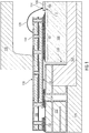
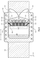
- FIG. 1 illustrates a partial sectional view of a semiconductor package, according to an embodiment.
- the semiconductor package includes a metal baseplate 100 having a die attach region 102 and a peripheral region 104, a transistor die 106 attached to the die attach region 102 of the baseplate 100, a multilayer circuit board 108 such as a PCB for providing electrical connections to the transistor die 106, and an optional lid 110 for enclosing the transistor die 106.
- the baseplate 100 is made of an electrically and thermally conductive material such as Cu, CPC (copper, copper-molybendum, copper laminate structure), CuW, etc.
- the transistor die 106 attached to the baseplate 100 is a power transistor die such as an RF amplifier die.
- the transistor die 106 can be an LDMOS (laterally diffused metal oxide semiconductor), vertical power MOSFET (metal oxide semiconductor field effect transistor) or GaN RF power transistor die.
- the transistor die 106 has a reference terminal 112 such as a source or emitter terminal attached to the die attach region 102 and an RF terminal 114 such as a drain or collector terminal facing away from the baseplate 100.
- the control (gate) terminal of the transistor die is out of view in Figure 1 .
- More than one transistor die can be attached to the baseplate 100, e.g., in the case of a Doherty amplifier in which a main and one or more peaking amplifiers can be attached to the baseplate 100.
- the multilayer circuit board 108 has a first side 116 attached to the peripheral region 104 of the baseplate 100 and a second side 118 facing away from the baseplate 100.
- the multilayer circuit board 108 extends beyond an exterior sidewall 120 of the baseplate 100 for attachment to another circuit board 122.
- the semiconductor package is connected to a global printed circuit board 122.
- the global printed circuit board 122 is part of a sub-system or system that incorporates the semiconductor package as a constituent component. Other semiconductor devices that are part of this sub-system or system can be connected to the global printed circuit board 122 as well.
- This global printed circuit board 122 can have a recessed region for receiving the baseplate 100 of the semiconductor package.
- a metal slug 124 can be disposed in the recess for enhancing the thermal and electrical conduction between the global printed circuit board 122 and the multilayer circuit board 108.
- the global printed circuit board 122 may include a heatsink 126 containing aluminium or copper, for example, which attaches to the baseplate 100 of the semiconductor package.
- the RF terminal 114 of the transistor die 106 is electrically connected to the multilayer circuit board 108, which in turn is connected to the global printed circuit board 122.
- an electrically conductive bond wire 128 forms a direct electrical connection between the RF terminal 114 of the transistor die 106 and a first bond pad 130 that is disposed on the second side 118 of the multilayer circuit board 108.
- the multilayer circuit board 108 further includes two pads 132, 134 disposed on the first side 116 of the multilayer circuit board. The first pad 132 directly faces and electrically connects to a signal pad of the global printed circuit board 122, and thus forms a signal connection between the two.
- the second pad 134 directly faces and electrically connects to a ground pad of the global printed circuit board 122 (as well as the baseplate 100), and thus forms a ground connection between the two.
- the multilayer circuit board 108 contains conductive signal layers and via structures that connect the first bond pad 130 and the second bond pad 132. Using these conductive layers, the multilayer circuit board 108 connects the RF terminal 114 of the transistor die 106 to the global printed circuit board 122.
- an RF impedance matching network can be embedded in the multilayer circuit board 108 and coupled to the RF terminal 114 of the transistor die 106 so as to match the impedance of the packaged device to a desired value (e.g., 50 ohms).
- the multilayer circuit board 108 includes a number of conductive layers. According to an embodiment, the multilayer circuit board 108 has four electrically conductive layers: a first signal layer 136; a first ground layer 138; a second signal layer 140; and a second ground layer 142. Each of these layers is formed from a standard conductive material, such as copper.
- the first signal layer 136 is disposed at the second side 118 of the multilayer circuit board 108 and the second ground layer 142 is disposed at the first side 116 of the multilayer circuit board 108.
- first signal layer 136 and the second ground layer 142 are disposed at outer, opposing sides of the multilayer circuit board 108.
- disposed at the first side or “disposed at the second side,” as the case may be, refers to the fact that outer side of the particular element is coextensive with the first or second side of the multilayer circuit board.
- the first ground layer 138 and the second signal layer 140 are embedded in the multilayer circuit board.
- embedded refers to the fact that the particular element is incorporated into the structure of the multilayer circuit board 108 and is separated from both the first side 116 and the second side 118 by another element or layer.
- the multilayer circuit board 108 includes a first embedded layer 144 disposed between the first signal layer 136 and the first ground layer 138. The first embedded layer 144 and the first signal layer 136 separate the first ground layer 138 from the second surface 118.
- the multilayer circuit board 108 includes a second embedded layer 146 disposed between the second signal layer 140 and the second ground layer 142.
- the second embedded layer 146 and the second ground layer 142 separate the second signal layer 140 from the first surface 116.
- the first embedded layer 144 and the second embedded layer 146 are formed from an insulative pre-impregnated composite fiber material, such as polytetrafluoroethylene, FR-1, FR-2, FR-3, FR-4, FR-5, FR-6, G-10, CEM-1, CEM-2, CEM-3, CEM-4, CEM-5, etc.
- the first and second embedded layers 144, 146 have a thickness of at least 75 ⁇ m and according to one embodiment, have a thickness of about 100 ⁇ m.
- the multilayer circuit board 108 further includes an embedded dielectric layer 148 disposed between the first ground layer 138 and the second signal layer 140.
- the first ground layer 138 and the second signal layer 140 are thus arranged in a parallel plate-capacitor configuration.
- the embedded dielectric layer 148 directly contacts the first ground layer 138 and the second signal layer 140.
- the embedded dielectric layer 148 is formed from a polymer capacitance laminate material with a high dielectric constant, e.g., between 4 and 30, and more particularly above 10 in some embodiments.
- the embedded dielectric layer 148 may have a thickness of between 2 ⁇ m and 50 ⁇ m, and more particularly between 2 ⁇ m and 24 ⁇ m is some embodiments.
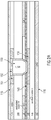
- the multilayer circuit board 108 also includes via structures for connecting and/or providing electrical access to various components. More particularly, Fig. 2A depicts an insulated signal via 150 for connecting sections of the first and second signal layers 136, 140 together.
- the insulated signal via 150 extends through the first embedded layer 144. Similar structures can be used to connect any two layers together.
- the insulated signal via 150 may include a cap 152 such as a copper cap in the case of a copper via and a top pad 154 adjacent the cap 152 in the first (uppermost) signal layer 136.
- the bottom of the insulated signal via 150 includes a conductive pad 156 that contacts a portion of the second signal layer 140.
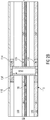
- Figure 2B illustrates a sectional view of an insulated path via 158 that extends from the first side 116 to the second side 118 and extends through all of the layers disposed between.
- the insulated path via 158 electrically contacts the second ground layer 142 by a conductive pad 156 and the first ground layer 138 by another conductive pad 156.
- the insulated path via 158 extends to the second side 118 in a region of the multilayer circuit board 108 that is a devoid of the first signal layer 136.
- the first and second ground layers 138, 142 are connected together and are electrically accessible at the second side 118 of the multilayer circuit board 108 by one of the conductive pads 156.
- a ground terminal of the multilayer circuit board 108 can be formed by the caps 220 on both sides of the multilayer circuit board 108.
- the circuit includes the transistor die 106 previously discussed with reference to Fig. 1 .
- the drain terminal of the transistor die 106 is electrically connected to the multilayer circuit board 108 by the electrically conductive bond wire 128 previously discussed with reference to Fig. 1 .
- the bond wire 128 connects to a first bond pad 154 of the multilayer circuit board 108, which may be formed in the first signal layer 136 and is represented by a first transmission line TL1 in the circuit schematic.
- the bond wire 128 is connected, via the first bond pad 154, to a shunt LC network 160 that is provided by the multilayer circuit board 108.
- the shunt LC network 160 includes reactive components that are configured to transform the output impedance of the circuit to a desired matching value (e.g., 50 ohms).
- the shunt LC network 160 includes a second transmission line TL2, which schematically represents one of the insulated signal vias 150 previously described.
- the second transmission line TL2 electrically connects the first transmission line TL1 (i.e., the top level bond pad) to an embedded reactive component that is integrated in multilayer circuit board 108.
- this embedded reactive component is an embedded capacitor C1.
- the positive electrode of the embedded capacitor C1 is formed by a first isolated section of the second signal layer 140, and the ground electrode of the first capacitor is formed by a first isolated section of the first ground layer 138.
- the embedded dielectric layer 148 is disposed between the two electrodes, i.e., so as to form a parallel plate capacitor described with reference to Fig. 2
- the first transmission line TL1 and the second transmission line TL2 are connected to a third transmission line TL3, which may be provided by another isolated section of the first signal layer 136.
- the third transmission line TL3 connects to a package terminal, which in turn may be connected to the global circuit board 122 described with reference to Fig. 1 .
- FIG. 4 an exemplary circuit topology is depicted, according to another embodiment.
- the circuit topology of Fig. 4 may be substantially similar or identical to that of Fig. 3 with the exception that the shunt LC network 160 is configured with a shunt inductor 162 and a radial stub 164.
- one of the insulated signal vias 150 connects the first transmission line TL1 (i.e., the top level bond pad) to a shunt inductor 162.
- the shunt inductor 162 may be provided by a linear strip of the second signal layer 140.
- the shunt inductor 162 connects to an open-circuit radial stub 164.
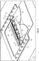
- a physical layout of the semiconductor package of Fig. 4 is depicted.
- similarly numbered elements refer to corresponding circuit elements schematically represented in Fig. 4 .
- a plurality of the bond wires 128 extend directly between the transistor die 106 and a plurality of bond pads 154 that are formed in the first signal layer 136. These bond pads 154 are electrically connected to the second signal layer 140 by insulated signal vias 150.
- the shunt inductor 162 and the open-circuit radial stub 164 are formed in the second signal layer 140 and connect to the bond pads 154 (and to the bond wires 128) by the insulated signal vias 150.
- the multilayer circuit board 108 may include a plurality of insulated path vias 158 as described with reference to Fig. 2B of the present Specification. These insulated path vias 158 are electrically connected to the ground layers to provide improved electrical isolation.
- radial stubs are used as open-circuit % wave terminations in RF circuits and have enhanced broadband frequency response.
- a radial stub can be formed on the top layer as a microstripline component (i.e., a thin flat conductor which is parallel to a ground plane).
- the relatively low equivalent dielectric constant in this kind of PCB 2 layer substrate means that compact radial stubs are not possible for certain frequency bands. That is, in conventional PCB 2 layer substrates, package area can become the gating factor for the radial stub.
- the presently configured multilayer circuit board 108 allows for the radial stub 164 to be configured as a stripline component (i.e., a flat strip of metal which is sandwiched between two parallel ground planes) with a relatively compact design.
- the embedded capacitance material substantially increases the capacitance per unit area of the stripline components and this leads a very compact radial stub layout.
- a layout of 2 mm 2 for the embedded component provides a capacitance of 100 pF, and this layout can be easily integrated inside a typical package outline of 10 mm x 7 mm (i.e., 70 mm 2 ).
- the radial stub layout area needed to achieve 100 pF is 200 mm 2 , and this size component cannot be integrated within a 10 mm x 7 mm package outline.
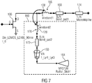
- FIG. 7 an exemplary circuit topology is depicted, according to another embodiment.
- the circuit of Fig. 7 differs from the circuit of Fig. 4 with respect to the configuration of the bond wires 128. More particularly, the bond wires 128 are configured with two separate branches. A first branch 166 of the bond wires 128 is directly connected between the RF terminal of the transistor die 106 and a first bond pad 168, which may be provided by a first isolated portion of the first signal layer 136 in the manner previously discussed. The first bond pad 168 is connected to an output node of the multilayer circuit board 108 by a length of microstripline 174.
- a second branch 170 of the bond wires 128 is directly connected between the RF terminal of the transistor die 106 and a second bond pad 172, which may be provided by a second isolated portion of the first signal layer 136 that is electrically disconnected from the first bond pad 168.
- An insulated signal via 150 connects the second bond pad 172 to the radial stub 164.
- a set of the first bond pads 168 may be arranged in a similar manner as the bond pads 154 shown in Figs. 5 and 6 .
- Another set of the second bond pads 172 may be disposed on either side of the first bond pads 168. That is, the first bond pads 168 may be disposed between the second bond pads 172.
- a plurality of insulated path vias 158 that are electrically grounded may be disposed between the first bond pads 168 and the second bond pads 172 to provide increased electrical shielding between the two.
- the first branch 166 of the bond wires 128 extends in a first direction D1 between the transistor die 106 and the first bond pads 168.
- the first direction D1 extends left to right, and represents a direction of the shortest path between the RF terminal 114 of the transistor die 106 and the first bond pads 168.
- the second branch 170 of the bond wires 128 extends in a second direction that is non-parallel to the first direction. That is, the second direction is disposed at an angle relative first direction.
- the second branch 170 of the bond wires 128 form an acute angle with the first branch 166 of the bond wires 128.
- This arrangement increases the separation distance between the first and second branches 176, 170 and consequently reduces the mutual inductance between the various bonding wires. As a result, parasitic effects are mitigated. Different orientations may be achieved, depending on the positioning of the bond pads 154.
- FIG. 10 an exemplary circuit topology is depicted, according to another embodiment.
- the circuit of Fig. 10 has a substantially similar topology to the circuit of Fig. 4 , with the exception that an additional capacitor 178 is incorporated into the output matching network to improve the linearity of the system by providing a low frequency termination.
- a low frequency termination capacitor can be provided outside of the package using a discrete component.
- this arrangement suffers from the drawback that the parasitic inductance and capacitance of the external electrical connections (e.g., bond wires) to the additional capacitor degrade the bandwidth of the low frequency termination by as much as 100 MHz to 200 MHz.
- the capacitor is disposed as close to the transistor as possible to mitigate these parasitic effects.
- the multilayer circuit board 108 design described herein allows for the additional capacitor 178 to be implemented as a discrete capacitor formed on or in the multilayer circuit board 108 very close to the transistor die 106. That is, the low frequency capacitor can incorporated into the device package. As a result, the bandwidth of the low frequency termination is improved.
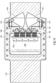
- the additional capacitor 178 is implemented as a surface-mount capacitor, i.e., a discrete capacitor with lower facing terminals that directly contact a bond pad, and is bonded to the second side 118 of the multilayer circuit board 108.
- the multilayer circuit board includes 108 a third bond pad 180 which is formed by a third isolated portion of the first signal layer 136.
- the third bond pad 180 is electrically disconnected from the other bond pads 154.
- a positive electrode of the low frequency termination capacitor 178 is electrically connected to at least one of the embedded reactive components (i.e., the shunt inductor 162 and the radial stub 164 in the embodiment of Figs. 11-12 ) by an insulated signal via 150.
- the negative electrode of the low frequency termination capacitor 178 is connected to electrical ground by one of the path vias 158.
- the multilayer circuit board 108 described herein provides the circuit topology of Fig. 10 in a space efficient manner by providing the radial stub 164 embedded within the multilayer circuit board 108 while using overlapping surface area on the top surface of the multilayer circuit board 108 for the low frequency termination capacitor 178.
- the low frequency termination capacitor 178 is combined with the circuit and corresponding layouts described with reference to Figs. 4-6 . However, this is just one example. Alternatively, the low frequency termination capacitor 178 could be combined with different configurations, such as the circuit and corresponding layouts described with reference to Figs. 7-9 .
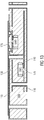
- the multilayer circuit board 108 may be configured similarly as the multilayer circuit board described with reference to Figs. 11 and 12 , with the exception that the low frequency termination capacitor 178 is disposed inside of the multilayer circuit board108 instead of on the upper surface.
- the low frequency termination capacitor 178 is an ultra-thin surface mount device. These devices can be embedded into the multilayer circuit board 108 during the fabrication process. More particularly, an ultra-thin surface mount device can be embedded in one or both of the embedded layers 144, 146, during the lamination process that forms these layers. Isolated sections of the signal and/or ground layers can be formed to provide bonding locations for the ultra-thin surface mount device.
- the insulated signal vias 150 and path vias 158 described herein can be used to connect these bonding locations with external bond pads.
Landscapes
- Engineering & Computer Science (AREA)
- Microelectronics & Electronic Packaging (AREA)
- Production Of Multi-Layered Print Wiring Board (AREA)
- Microwave Amplifiers (AREA)
Claims (14)
- Amplificateur Doherty, comprenant :une plaque de base métallique (100) ayant une région d'attache de puce (102) et une région périphérique (104) ;un amplificateur principal et un ou plusieurs amplificateurs de crête, dans lequel chaque amplificateur comprend un puce de transistor (106) attachée à la région d'attache de puce (102), chaque puce de transistor incluant au moins une borne RF (114) faisant face à l'opposé de la plaque de base (100) ;une carte de circuit imprimé à couches multiples (108) comprenant :une première face (116) attachée à la région périphérique (104) ;une seconde face (118) faisant face à l'opposé de la plaque de base (100) ;une première couche électriquement conductrice encastrée (138) qui est séparée de la seconde face (118) par une première couche de fibre composite encastrée (144) ;une seconde couche électriquement conductrice encastrée (140) qui est séparée de la première face (116) par une seconde couche de fibre composite encastrée (146) ; etune couche diélectrique encastrée (148) qui est disposée entre les première et seconde couches électriquement conductrices encastrées (144, 146), et qui a une constante diélectrique plus élevée que l'une ou l'autre des première et seconde couches de fibre composite encastrées (144, 146) ;un réseau d'adaptation d'impédance RF qui est électriquement connecté à une borne RF (114) d'au moins une des puces de transistor d'amplificateur (106), et qui comprend un ou plusieurs composants réactifs (C1, L1) formés à partir d'au moins une des couches électriquement conductrices encastrées.
- Amplificateur Doherty selon la revendication 1, dans lequel la carte de circuit imprimé à couches multiples (108) comprend en outre :une première couche de signal électriquement conductrice (136) disposée sur la seconde face (118) ; etune seconde couche de mise à la terre électriquement conductrice (142) disposée sur la première face (116) ; etdans lequel la première couche électriquement conductrice encastrée est une première couche de mise à la terre ; etdans lequel la seconde couche électriquement conductrice encastrée est une seconde couche de signal.
- Amplificateur Doherty selon la revendication 2, dans lequel :la première couche de fibre composite (144) sépare la première couche de signal (136) de la première couche de mise à la terre (138) ;la seconde couche de fibre composite (146) sépare la seconde couche de signal (140) de la seconde couche de mise à la terre (142) ; etdans lequel l'épaisseur de la couche diélectrique encastrée (148) est inférieure à l'épaisseur de la première couche de fibre composite encastrée (144) et inférieure à l'épaisseur de la seconde couche de fibre composite encastrée (146).
- Amplificateur Doherty selon la revendication 1, dans lequel la couche diélectrique encastrée (148) a une constante diélectrique d'entre 4 et 30, et dans lequel chacune des première et seconde couches de fibre composite encastrées (144, 146) a une constante diélectrique de 3,7 ou moins.
- Amplificateur Doherty selon la revendication 1, dans lequel la couche diélectrique encastrée (148) est formée à partir d'un matériau stratifié polymère, et dans lequel les première et seconde couches de fibre composite encastrées (144, 146) sont formées à partir d'au moins un de : FR-1, FR-2, FR-3, FR-4, FR-5, FR-6, G-10, CEM-1, CEM-2, CEM-3, CEM-4, CEM-5.
- Amplificateur Doherty selon la revendication 1, dans lequel la couche diélectrique encastrée (148) a une épaisseur d'entre 4 µm et 50 µm, et dans lequel chacune des première et seconde couches de fibre composite encastrées (144, 146) a une épaisseur d'au moins 75 µm.
- Amplificateur Doherty selon la revendication 2, dans lequel :la carte de circuit imprimé à couches multiples (108) comprend en outre un premier trou d'interconnexion électriquement conducteur (150) s'étendant à travers la première couche de fibre composite encastrée (144) et connecté à un première plage de contact (154) ;la première plage de contact (154) est formée par une section isolée de la première couche de signal (136) ; etchacun des un ou plusieurs composants réactifs (C1, L1) est électriquement connecté au premier trou d'interconnexion (150) et comprend une section isolée de la seconde couche de signal (140).
- Amplificateur Doherty selon la revendication 7, dans lequel :les un ou plusieurs composants réactifs (C1, L1) comprennent un premier condensateur (C1) ayant une électrode positive et une électrode de mise à la terre ;l'électrode positive est formée par une première section isolée de la seconde couche de signal (140) ; etl'électrode de mise à la terre est formée par une première section isolée de la première couche de mise à la terre (138).
- Amplificateur Doherty selon la revendication 7, dans lequel les un ou plusieurs composants réactifs (C1, L1) comprennent :une inductance de shuntage (162) comprenant une bande linéaire de la seconde couche de signal (140) ; etun bout radial de circuit ouvert (164) connecté à l'inductance de shuntage (162) et comprenant une portion de forme radiale de la seconde couche de signal (140).
- Amplificateur Doherty selon la revendication 9, comprenant en outre un premier ensemble (166) de fils de contact (128) directement connectés entre la borne RF (114) et la première plage de contact (154).
- Amplificateur Doherty selon la revendication 10, comprenant en outre :une deuxième plage de contact (172) formée par une portion isolée de la première couche de signal (136) ; etun second ensemble (170) de fils de contact (128) directement connectés entre la borne RF (114) et la deuxième plage de contact (172), dans lequel :le premier ensemble de fils de contact (18) s'étend dans une première direction entre la borne RF (114) et la première plage de contact (154),le second ensemble de fils de contact (128) s'étend dans une seconde direction entre la borne RF (114) et la deuxième plage de contact (172), etla seconde direction est non parallèle à la première direction.
- Amplificateur Doherty selon la revendication 7, comprenant en outre un condensateur distinct (178) formé sur ou dans la plaque de base (100) et connecté aux un ou plusieurs composants réactifs (C1, L1).
- Amplificateur Doherty selon la revendication 12, dans lequel :la carte de circuit imprimé à couches multiples (108) comprend une troisième plage de contact (180) formée par une portion isolée de la première couche de signal (136) ;le condensateur distinct (178) est un condensateur pour montage en surface qui est directement monté sur la troisième plage de contact (180) ; etla troisième plage de contact (180) est électriquement connectée aux un ou plusieurs composants réactifs (C1, L1) par un second trou d'interconnexion électriquement conducteur s'étendant à travers la première couche de fibre composite encastrée (144).
- Ensemble à amplificateur Doherty, comprenant :l'amplificateur Doherty selon la revendication 1 ; etune carte de circuit imprimé globale (122),dans lequel la carte de circuit imprimé à couches multiples (108) connecte les bornes RF (114) des puces de transistor d'amplificateur respective (106) à la carte de circuit imprimé globale.
Applications Claiming Priority (3)
| Application Number | Priority Date | Filing Date | Title |
|---|---|---|---|
| US15/046,923 US10225922B2 (en) | 2016-02-18 | 2016-02-18 | PCB based semiconductor package with impedance matching network elements integrated therein |
| PCT/EP2017/053424 WO2017140737A1 (fr) | 2016-02-18 | 2017-02-15 | Boîtier de semi-conducteur à base de pcb avec éléments de réseau d'adaptation d'impédance intégrés dedans |
| EP17705143.0A EP3398206B1 (fr) | 2016-02-18 | 2017-02-15 | Boîtier semi-conducteur incluant un circuit imprimé dans lequel des éléments de réseau d'adaptation d'impédance sont intégrés |
Related Parent Applications (2)
| Application Number | Title | Priority Date | Filing Date |
|---|---|---|---|
| EP17705143.0A Division EP3398206B1 (fr) | 2016-02-18 | 2017-02-15 | Boîtier semi-conducteur incluant un circuit imprimé dans lequel des éléments de réseau d'adaptation d'impédance sont intégrés |
| EP17705143.0A Division-Into EP3398206B1 (fr) | 2016-02-18 | 2017-02-15 | Boîtier semi-conducteur incluant un circuit imprimé dans lequel des éléments de réseau d'adaptation d'impédance sont intégrés |
Publications (2)
| Publication Number | Publication Date |
|---|---|
| EP3640982A1 EP3640982A1 (fr) | 2020-04-22 |
| EP3640982B1 true EP3640982B1 (fr) | 2021-01-13 |
Family
ID=58044093
Family Applications (2)
| Application Number | Title | Priority Date | Filing Date |
|---|---|---|---|
| EP19207270.0A Active EP3640982B1 (fr) | 2016-02-18 | 2017-02-15 | Amplicateur doherty basé sur une carte de circuit imprimé avec des éléments de réseau d'adaptation d'impédance intégrés dans la carte de circuit imprimé |
| EP17705143.0A Active EP3398206B1 (fr) | 2016-02-18 | 2017-02-15 | Boîtier semi-conducteur incluant un circuit imprimé dans lequel des éléments de réseau d'adaptation d'impédance sont intégrés |
Family Applications After (1)
| Application Number | Title | Priority Date | Filing Date |
|---|---|---|---|
| EP17705143.0A Active EP3398206B1 (fr) | 2016-02-18 | 2017-02-15 | Boîtier semi-conducteur incluant un circuit imprimé dans lequel des éléments de réseau d'adaptation d'impédance sont intégrés |
Country Status (5)
| Country | Link |
|---|---|
| US (3) | US10225922B2 (fr) |
| EP (2) | EP3640982B1 (fr) |
| KR (1) | KR102093572B1 (fr) |
| CN (1) | CN108701683B (fr) |
| WO (1) | WO2017140737A1 (fr) |
Families Citing this family (14)
| Publication number | Priority date | Publication date | Assignee | Title |
|---|---|---|---|---|
| US20170325327A1 (en) * | 2016-04-07 | 2017-11-09 | Massachusetts Institute Of Technology | Printed circuit board for high power components |
| US10141303B1 (en) * | 2017-09-20 | 2018-11-27 | Cree, Inc. | RF amplifier package with biasing strip |
| US12283555B2 (en) | 2018-03-23 | 2025-04-22 | Analog Devices International Unlimited Company | Semiconductor packages |
| JP2020205519A (ja) * | 2019-06-17 | 2020-12-24 | 株式会社村田製作所 | 回路基板、インダクタおよび無線装置 |
| US11503704B2 (en) * | 2019-12-30 | 2022-11-15 | General Electric Company | Systems and methods for hybrid glass and organic packaging for radio frequency electronics |
| US12500562B2 (en) | 2020-04-03 | 2025-12-16 | Macom Technology Solutions Holdings, Inc. | RF amplifier devices and methods of manufacturing including modularized designs with flip chip interconnections |
| US11356070B2 (en) | 2020-06-01 | 2022-06-07 | Wolfspeed, Inc. | RF amplifiers having shielded transmission line structures |
| US11670605B2 (en) | 2020-04-03 | 2023-06-06 | Wolfspeed, Inc. | RF amplifier devices including interconnect structures and methods of manufacturing |
| US11837457B2 (en) | 2020-09-11 | 2023-12-05 | Wolfspeed, Inc. | Packaging for RF transistor amplifiers |
| US12166003B2 (en) | 2020-04-03 | 2024-12-10 | Macom Technology Solutions Holdings, Inc. | RF amplifier devices including top side contacts and methods of manufacturing |
| US12100630B2 (en) | 2020-11-13 | 2024-09-24 | Macom Technology Solutions Holdings, Inc. | Packaged RF power device with PCB routing outside protective member |
| US20230344393A1 (en) * | 2022-04-08 | 2023-10-26 | Skyworks Solutions, Inc. | Power amplifier systems with frequency response compensation |
| EP4343831A1 (fr) * | 2022-09-25 | 2024-03-27 | Wolfspeed, Inc. | Transistor à effet de champ à capacité série intégrée |
| CN117812804A (zh) * | 2022-09-26 | 2024-04-02 | 鹏鼎控股(深圳)股份有限公司 | 电路板及其制造方法 |
Family Cites Families (45)
| Publication number | Priority date | Publication date | Assignee | Title |
|---|---|---|---|---|
| US3986196A (en) | 1975-06-30 | 1976-10-12 | Varian Associates | Through-substrate source contact for microwave FET |
| JPH07123177B2 (ja) * | 1986-08-29 | 1995-12-25 | 日立化成工業株式会社 | 高周波回路用基板の製造法 |
| US5067004A (en) * | 1989-12-13 | 1991-11-19 | Digital Equipment Corporation | Module for interconnecting integrated circuits |
| DE69318879T2 (de) | 1992-04-03 | 1998-10-08 | Matsushita Electric Ind Co Ltd | Keramisches Mehrschicht-Substrat für hohe Frequenzen |
| JPH06295962A (ja) | 1992-10-20 | 1994-10-21 | Ibiden Co Ltd | 電子部品搭載用基板およびその製造方法並びに電子部品搭載装置 |
| US5622588A (en) | 1995-02-02 | 1997-04-22 | Hestia Technologies, Inc. | Methods of making multi-tier laminate substrates for electronic device packaging |
| US5597643A (en) | 1995-03-13 | 1997-01-28 | Hestia Technologies, Inc. | Multi-tier laminate substrate with internal heat spreader |
| US5609889A (en) | 1995-05-26 | 1997-03-11 | Hestia Technologies, Inc. | Apparatus for encapsulating electronic packages |
| US5843808A (en) | 1996-01-11 | 1998-12-01 | Asat, Limited | Structure and method for automated assembly of a tab grid array package |
| JPH10242377A (ja) | 1997-02-25 | 1998-09-11 | Hitachi Ltd | 高周波電力増幅器モジュール |
| US5973389A (en) | 1997-04-22 | 1999-10-26 | International Business Machines Corporation | Semiconductor chip carrier assembly |
| JP3732927B2 (ja) * | 1997-07-31 | 2006-01-11 | 京セラ株式会社 | 多層配線基板 |
| US6691296B1 (en) * | 1998-02-02 | 2004-02-10 | Matsushita Electric Industrial Co., Ltd. | Circuit board design aiding |
| US6329713B1 (en) | 1998-10-21 | 2001-12-11 | International Business Machines Corporation | Integrated circuit chip carrier assembly comprising a stiffener attached to a dielectric substrate |
| JP3214472B2 (ja) * | 1998-12-04 | 2001-10-02 | 日本電気株式会社 | 多層プリント回路基板 |
| US6261868B1 (en) | 1999-04-02 | 2001-07-17 | Motorola, Inc. | Semiconductor component and method for manufacturing the semiconductor component |
| JP3232562B2 (ja) * | 1999-10-22 | 2001-11-26 | 日本電気株式会社 | 電磁干渉抑制部品および電磁干渉抑制回路 |
| EP1265466A3 (fr) * | 2001-06-05 | 2004-07-21 | Dai Nippon Printing Co., Ltd. | Procédé de fabrication d'un panneau à circuit muni d'éléments passifs et panneau à circuit muni d'éléments passifs |
| US6511866B1 (en) | 2001-07-12 | 2003-01-28 | Rjr Polymers, Inc. | Use of diverse materials in air-cavity packaging of electronic devices |
| US6847527B2 (en) | 2001-08-24 | 2005-01-25 | 3M Innovative Properties Company | Interconnect module with reduced power distribution impedance |
| JP2003068571A (ja) * | 2001-08-27 | 2003-03-07 | Nec Corp | 可変コンデンサおよび可変インダクタ並びにそれらを備えた高周波回路モジュール |
| JP4079699B2 (ja) * | 2001-09-28 | 2008-04-23 | 富士通株式会社 | 多層配線回路基板 |
| US6633005B2 (en) | 2001-10-22 | 2003-10-14 | Micro Mobio Corporation | Multilayer RF amplifier module |
| JP2003179181A (ja) | 2001-12-11 | 2003-06-27 | Ngk Spark Plug Co Ltd | 樹脂製配線基板 |
| JP3813098B2 (ja) | 2002-02-14 | 2006-08-23 | 三菱電機株式会社 | 電力用半導体モジュール |
| DE10223035A1 (de) | 2002-05-22 | 2003-12-04 | Infineon Technologies Ag | Elektronisches Bauteil mit Hohlraumgehäuse, insbesondere Hochfrequenz-Leistungsmodul |
| US7298046B2 (en) | 2003-01-10 | 2007-11-20 | Kyocera America, Inc. | Semiconductor package having non-ceramic based window frame |
| US7446411B2 (en) | 2005-10-24 | 2008-11-04 | Freescale Semiconductor, Inc. | Semiconductor structure and method of assembly |
| US8238116B2 (en) | 2007-04-13 | 2012-08-07 | Avx Corporation | Land grid feedthrough low ESL technology |
| US7728774B2 (en) | 2008-07-07 | 2010-06-01 | International Business Machines Corporation | Radio frequency (RF) integrated circuit (IC) packages having characteristics suitable for mass production |
| WO2010144792A1 (fr) * | 2009-06-11 | 2010-12-16 | Rogers Corporation | Matériaux diélectriques, procédés de fabrication de sous-ensembles à partir de ceux-ci et sous-ensembles formés à partir de ceux-ci |
| US8013429B2 (en) | 2009-07-14 | 2011-09-06 | Infineon Technologies Ag | Air cavity package with copper heat sink and ceramic window frame |
| US8110915B2 (en) | 2009-10-16 | 2012-02-07 | Infineon Technologies Ag | Open cavity leadless surface mountable package for high power RF applications |
| JP5146627B2 (ja) * | 2011-02-15 | 2013-02-20 | 株式会社村田製作所 | 多層配線基板およびその製造方法 |
| JP5784722B2 (ja) * | 2011-06-29 | 2015-09-24 | 日本碍子株式会社 | 大容量モジュールの周辺回路用の回路基板、及び当該回路基板を用いる周辺回路を含む大容量モジュール |
| JP5765174B2 (ja) | 2011-09-30 | 2015-08-19 | 富士通株式会社 | 電子装置 |
| US8907467B2 (en) | 2012-03-28 | 2014-12-09 | Infineon Technologies Ag | PCB based RF-power package window frame |
| KR20130113032A (ko) * | 2012-04-05 | 2013-10-15 | 에스케이하이닉스 주식회사 | 반도체 기판, 이를 갖는 반도체 칩 및 적층 반도체 패키지 |
| KR20140008871A (ko) * | 2012-07-12 | 2014-01-22 | 삼성전기주식회사 | 빌드업 절연필름용 에폭시 수지 조성물, 이로부터 제조된 절연 필름 및 이를 구비한 다층 인쇄회로기판 |
| US9196958B2 (en) * | 2012-07-26 | 2015-11-24 | Apple Inc. | Antenna structures and shield layers on packaged wireless circuits |
| JP2014060244A (ja) * | 2012-09-18 | 2014-04-03 | Sony Corp | 多層プリント配線基板 |
| CN103795384B (zh) * | 2012-10-31 | 2017-04-19 | 台达电子企业管理(上海)有限公司 | 开关电路封装模块 |
| KR101442354B1 (ko) | 2012-12-21 | 2014-09-17 | 삼성전기주식회사 | 예비 공간 변환기 및 이를 이용하여 제조된 공간 변환기, 그리고 상기 공간 변환기를 구비하는 반도체 소자 검사 장치 |
| CN104066265A (zh) * | 2013-03-22 | 2014-09-24 | 叶云照 | 多层印刷电路板结构 |
| US9629246B2 (en) * | 2015-07-28 | 2017-04-18 | Infineon Technologies Ag | PCB based semiconductor package having integrated electrical functionality |
-
2016
- 2016-02-18 US US15/046,923 patent/US10225922B2/en active Active
-
2017
- 2017-02-15 EP EP19207270.0A patent/EP3640982B1/fr active Active
- 2017-02-15 CN CN201780012179.4A patent/CN108701683B/zh active Active
- 2017-02-15 KR KR1020187025730A patent/KR102093572B1/ko active Active
- 2017-02-15 EP EP17705143.0A patent/EP3398206B1/fr active Active
- 2017-02-15 WO PCT/EP2017/053424 patent/WO2017140737A1/fr not_active Ceased
-
2018
- 2018-12-04 US US16/209,018 patent/US10575394B2/en active Active
-
2019
- 2019-12-31 US US16/731,370 patent/US10743404B2/en active Active
Non-Patent Citations (1)
| Title |
|---|
| None * |
Also Published As
| Publication number | Publication date |
|---|---|
| US20200137877A1 (en) | 2020-04-30 |
| US20190110358A1 (en) | 2019-04-11 |
| US10575394B2 (en) | 2020-02-25 |
| EP3640982A1 (fr) | 2020-04-22 |
| EP3398206B1 (fr) | 2019-12-11 |
| US10743404B2 (en) | 2020-08-11 |
| EP3398206A1 (fr) | 2018-11-07 |
| KR20180114097A (ko) | 2018-10-17 |
| KR102093572B1 (ko) | 2020-03-25 |
| US20170245359A1 (en) | 2017-08-24 |
| US10225922B2 (en) | 2019-03-05 |
| CN108701683A (zh) | 2018-10-23 |
| WO2017140737A1 (fr) | 2017-08-24 |
| CN108701683B (zh) | 2021-08-13 |
Similar Documents
| Publication | Publication Date | Title |
|---|---|---|
| EP3640982B1 (fr) | Amplicateur doherty basé sur une carte de circuit imprimé avec des éléments de réseau d'adaptation d'impédance intégrés dans la carte de circuit imprimé | |
| CN109994436B (zh) | 具有集成电气功能的基于pcb的半导体封装 | |
| EP3096353B1 (fr) | Dispositif de circuit de sortie d'un amplificateur rf avec une piste intégrée pour la circulation du courant | |
| US9820401B2 (en) | Packaged RF power transistor device having next to each other a ground and a video lead for connecting a decoupling capacitor, RF power amplifier | |
| CN103681635B (zh) | 具有阻抗匹配电路的半导体装置及其制造方法 | |
| US9799599B2 (en) | Matching techniques for wide-bandgap power transistors | |
| EP3213411B1 (fr) | Réseau d'adaptation de sortie ayant un seul composant condensateur combiné en série et shunt | |
| EP2722880B1 (fr) | Circuit amplificateur en boîtier | |
| US20200251393A1 (en) | Package and semiconductor device | |
| US20240292520A1 (en) | Matching circuit board and semiconductor device | |
| JP7747177B2 (ja) | 電子部品及び回路装置 | |
| US20250125286A1 (en) | Semiconductor device | |
| US20200343616A1 (en) | Frequency selective capacitively tuned ground bonds for high isolation in rf devices | |
| JP2004282171A (ja) | 広帯域直流成分除去回路及びその組立方法 | |
| WO2006072984A1 (fr) | Amplificateur a semi-conducteur | |
| HK1196462A (en) | Improved matching techniques for wide-bandgap power transistors |
Legal Events
| Date | Code | Title | Description |
|---|---|---|---|
| PUAI | Public reference made under article 153(3) epc to a published international application that has entered the european phase |
Free format text: ORIGINAL CODE: 0009012 |
|
| STAA | Information on the status of an ep patent application or granted ep patent |
Free format text: STATUS: THE APPLICATION HAS BEEN PUBLISHED |
|
| AC | Divisional application: reference to earlier application |
Ref document number: 3398206 Country of ref document: EP Kind code of ref document: P |
|
| AK | Designated contracting states |
Kind code of ref document: A1 Designated state(s): AL AT BE BG CH CY CZ DE DK EE ES FI FR GB GR HR HU IE IS IT LI LT LU LV MC MK MT NL NO PL PT RO RS SE SI SK SM TR |
|
| STAA | Information on the status of an ep patent application or granted ep patent |
Free format text: STATUS: REQUEST FOR EXAMINATION WAS MADE |
|
| 17P | Request for examination filed |
Effective date: 20200615 |
|
| RBV | Designated contracting states (corrected) |
Designated state(s): AL AT BE BG CH CY CZ DE DK EE ES FI FR GB GR HR HU IE IS IT LI LT LU LV MC MK MT NL NO PL PT RO RS SE SI SK SM TR |
|
| RIC1 | Information provided on ipc code assigned before grant |
Ipc: H05K 1/16 20060101ALI20200626BHEP Ipc: H05K 1/02 20060101ALI20200626BHEP Ipc: H05K 1/11 20060101ALI20200626BHEP Ipc: H01L 23/498 20060101ALI20200626BHEP Ipc: H01L 23/66 20060101AFI20200626BHEP Ipc: H01L 23/13 20060101ALI20200626BHEP |
|
| GRAP | Despatch of communication of intention to grant a patent |
Free format text: ORIGINAL CODE: EPIDOSNIGR1 |
|
| STAA | Information on the status of an ep patent application or granted ep patent |
Free format text: STATUS: GRANT OF PATENT IS INTENDED |
|
| INTG | Intention to grant announced |
Effective date: 20200812 |
|
| GRAS | Grant fee paid |
Free format text: ORIGINAL CODE: EPIDOSNIGR3 |
|
| GRAA | (expected) grant |
Free format text: ORIGINAL CODE: 0009210 |
|
| STAA | Information on the status of an ep patent application or granted ep patent |
Free format text: STATUS: THE PATENT HAS BEEN GRANTED |
|
| AC | Divisional application: reference to earlier application |
Ref document number: 3398206 Country of ref document: EP Kind code of ref document: P |
|
| AK | Designated contracting states |
Kind code of ref document: B1 Designated state(s): AL AT BE BG CH CY CZ DE DK EE ES FI FR GB GR HR HU IE IS IT LI LT LU LV MC MK MT NL NO PL PT RO RS SE SI SK SM TR |
|
| REG | Reference to a national code |
Ref country code: GB Ref legal event code: FG4D |
|
| REG | Reference to a national code |
Ref country code: CH Ref legal event code: EP |
|
| REG | Reference to a national code |
Ref country code: IE Ref legal event code: FG4D |
|
| REG | Reference to a national code |
Ref country code: DE Ref legal event code: R096 Ref document number: 602017031542 Country of ref document: DE |
|
| REG | Reference to a national code |
Ref country code: AT Ref legal event code: REF Ref document number: 1355183 Country of ref document: AT Kind code of ref document: T Effective date: 20210215 |
|
| REG | Reference to a national code |
Ref country code: FI Ref legal event code: FGE |
|
| REG | Reference to a national code |
Ref country code: SE Ref legal event code: TRGR |
|
| REG | Reference to a national code |
Ref country code: AT Ref legal event code: MK05 Ref document number: 1355183 Country of ref document: AT Kind code of ref document: T Effective date: 20210113 |
|
| REG | Reference to a national code |
Ref country code: NL Ref legal event code: MP Effective date: 20210113 |
|
| REG | Reference to a national code |
Ref country code: LT Ref legal event code: MG9D |
|
| PG25 | Lapsed in a contracting state [announced via postgrant information from national office to epo] |
Ref country code: HR Free format text: LAPSE BECAUSE OF FAILURE TO SUBMIT A TRANSLATION OF THE DESCRIPTION OR TO PAY THE FEE WITHIN THE PRESCRIBED TIME-LIMIT Effective date: 20210113 Ref country code: BG Free format text: LAPSE BECAUSE OF FAILURE TO SUBMIT A TRANSLATION OF THE DESCRIPTION OR TO PAY THE FEE WITHIN THE PRESCRIBED TIME-LIMIT Effective date: 20210413 Ref country code: GR Free format text: LAPSE BECAUSE OF FAILURE TO SUBMIT A TRANSLATION OF THE DESCRIPTION OR TO PAY THE FEE WITHIN THE PRESCRIBED TIME-LIMIT Effective date: 20210414 Ref country code: NO Free format text: LAPSE BECAUSE OF FAILURE TO SUBMIT A TRANSLATION OF THE DESCRIPTION OR TO PAY THE FEE WITHIN THE PRESCRIBED TIME-LIMIT Effective date: 20210413 Ref country code: PT Free format text: LAPSE BECAUSE OF FAILURE TO SUBMIT A TRANSLATION OF THE DESCRIPTION OR TO PAY THE FEE WITHIN THE PRESCRIBED TIME-LIMIT Effective date: 20210513 Ref country code: LT Free format text: LAPSE BECAUSE OF FAILURE TO SUBMIT A TRANSLATION OF THE DESCRIPTION OR TO PAY THE FEE WITHIN THE PRESCRIBED TIME-LIMIT Effective date: 20210113 |
|
| PG25 | Lapsed in a contracting state [announced via postgrant information from national office to epo] |
Ref country code: RS Free format text: LAPSE BECAUSE OF FAILURE TO SUBMIT A TRANSLATION OF THE DESCRIPTION OR TO PAY THE FEE WITHIN THE PRESCRIBED TIME-LIMIT Effective date: 20210113 Ref country code: AT Free format text: LAPSE BECAUSE OF FAILURE TO SUBMIT A TRANSLATION OF THE DESCRIPTION OR TO PAY THE FEE WITHIN THE PRESCRIBED TIME-LIMIT Effective date: 20210113 Ref country code: PL Free format text: LAPSE BECAUSE OF FAILURE TO SUBMIT A TRANSLATION OF THE DESCRIPTION OR TO PAY THE FEE WITHIN THE PRESCRIBED TIME-LIMIT Effective date: 20210113 Ref country code: LV Free format text: LAPSE BECAUSE OF FAILURE TO SUBMIT A TRANSLATION OF THE DESCRIPTION OR TO PAY THE FEE WITHIN THE PRESCRIBED TIME-LIMIT Effective date: 20210113 |
|
| PG25 | Lapsed in a contracting state [announced via postgrant information from national office to epo] |
Ref country code: IS Free format text: LAPSE BECAUSE OF FAILURE TO SUBMIT A TRANSLATION OF THE DESCRIPTION OR TO PAY THE FEE WITHIN THE PRESCRIBED TIME-LIMIT Effective date: 20210513 |
|
| REG | Reference to a national code |
Ref country code: DE Ref legal event code: R097 Ref document number: 602017031542 Country of ref document: DE |
|
| REG | Reference to a national code |
Ref country code: BE Ref legal event code: MM Effective date: 20210228 |
|
| PG25 | Lapsed in a contracting state [announced via postgrant information from national office to epo] |
Ref country code: LI Free format text: LAPSE BECAUSE OF NON-PAYMENT OF DUE FEES Effective date: 20210228 Ref country code: MC Free format text: LAPSE BECAUSE OF FAILURE TO SUBMIT A TRANSLATION OF THE DESCRIPTION OR TO PAY THE FEE WITHIN THE PRESCRIBED TIME-LIMIT Effective date: 20210113 Ref country code: LU Free format text: LAPSE BECAUSE OF NON-PAYMENT OF DUE FEES Effective date: 20210215 Ref country code: CZ Free format text: LAPSE BECAUSE OF FAILURE TO SUBMIT A TRANSLATION OF THE DESCRIPTION OR TO PAY THE FEE WITHIN THE PRESCRIBED TIME-LIMIT Effective date: 20210113 Ref country code: EE Free format text: LAPSE BECAUSE OF FAILURE TO SUBMIT A TRANSLATION OF THE DESCRIPTION OR TO PAY THE FEE WITHIN THE PRESCRIBED TIME-LIMIT Effective date: 20210113 Ref country code: CH Free format text: LAPSE BECAUSE OF NON-PAYMENT OF DUE FEES Effective date: 20210228 Ref country code: SM Free format text: LAPSE BECAUSE OF FAILURE TO SUBMIT A TRANSLATION OF THE DESCRIPTION OR TO PAY THE FEE WITHIN THE PRESCRIBED TIME-LIMIT Effective date: 20210113 |
|
| PLBE | No opposition filed within time limit |
Free format text: ORIGINAL CODE: 0009261 |
|
| STAA | Information on the status of an ep patent application or granted ep patent |
Free format text: STATUS: NO OPPOSITION FILED WITHIN TIME LIMIT |
|
| PG25 | Lapsed in a contracting state [announced via postgrant information from national office to epo] |
Ref country code: DK Free format text: LAPSE BECAUSE OF FAILURE TO SUBMIT A TRANSLATION OF THE DESCRIPTION OR TO PAY THE FEE WITHIN THE PRESCRIBED TIME-LIMIT Effective date: 20210113 Ref country code: SK Free format text: LAPSE BECAUSE OF FAILURE TO SUBMIT A TRANSLATION OF THE DESCRIPTION OR TO PAY THE FEE WITHIN THE PRESCRIBED TIME-LIMIT Effective date: 20210113 Ref country code: RO Free format text: LAPSE BECAUSE OF FAILURE TO SUBMIT A TRANSLATION OF THE DESCRIPTION OR TO PAY THE FEE WITHIN THE PRESCRIBED TIME-LIMIT Effective date: 20210113 |
|
| 26N | No opposition filed |
Effective date: 20211014 |
|
| GBPC | Gb: european patent ceased through non-payment of renewal fee |
Effective date: 20210413 |
|
| PG25 | Lapsed in a contracting state [announced via postgrant information from national office to epo] |
Ref country code: IE Free format text: LAPSE BECAUSE OF NON-PAYMENT OF DUE FEES Effective date: 20210215 Ref country code: AL Free format text: LAPSE BECAUSE OF FAILURE TO SUBMIT A TRANSLATION OF THE DESCRIPTION OR TO PAY THE FEE WITHIN THE PRESCRIBED TIME-LIMIT Effective date: 20210113 Ref country code: GB Free format text: LAPSE BECAUSE OF NON-PAYMENT OF DUE FEES Effective date: 20210413 Ref country code: FR Free format text: LAPSE BECAUSE OF NON-PAYMENT OF DUE FEES Effective date: 20210313 Ref country code: ES Free format text: LAPSE BECAUSE OF FAILURE TO SUBMIT A TRANSLATION OF THE DESCRIPTION OR TO PAY THE FEE WITHIN THE PRESCRIBED TIME-LIMIT Effective date: 20210113 |
|
| PG25 | Lapsed in a contracting state [announced via postgrant information from national office to epo] |
Ref country code: SI Free format text: LAPSE BECAUSE OF FAILURE TO SUBMIT A TRANSLATION OF THE DESCRIPTION OR TO PAY THE FEE WITHIN THE PRESCRIBED TIME-LIMIT Effective date: 20210113 |
|
| PG25 | Lapsed in a contracting state [announced via postgrant information from national office to epo] |
Ref country code: IS Free format text: LAPSE BECAUSE OF FAILURE TO SUBMIT A TRANSLATION OF THE DESCRIPTION OR TO PAY THE FEE WITHIN THE PRESCRIBED TIME-LIMIT Effective date: 20210513 |
|
| PG25 | Lapsed in a contracting state [announced via postgrant information from national office to epo] |
Ref country code: BE Free format text: LAPSE BECAUSE OF NON-PAYMENT OF DUE FEES Effective date: 20210228 |
|
| REG | Reference to a national code |
Ref country code: DE Ref legal event code: R081 Ref document number: 602017031542 Country of ref document: DE Owner name: WOLFSPEED, INC., DURHAM, US Free format text: FORMER OWNER: CREE, INC., DURHAM, N.C., US Ref country code: DE Ref legal event code: R081 Ref document number: 602017031542 Country of ref document: DE Owner name: MACOM TECHNOLOGY SOLUTIONS HOLDINGS, INC., LOW, US Free format text: FORMER OWNER: CREE, INC., DURHAM, N.C., US |
|
| PG25 | Lapsed in a contracting state [announced via postgrant information from national office to epo] |
Ref country code: NL Free format text: LAPSE BECAUSE OF NON-PAYMENT OF DUE FEES Effective date: 20210113 Ref country code: CY Free format text: LAPSE BECAUSE OF FAILURE TO SUBMIT A TRANSLATION OF THE DESCRIPTION OR TO PAY THE FEE WITHIN THE PRESCRIBED TIME-LIMIT Effective date: 20210113 |
|
| P01 | Opt-out of the competence of the unified patent court (upc) registered |
Effective date: 20230801 |
|
| PG25 | Lapsed in a contracting state [announced via postgrant information from national office to epo] |
Ref country code: HU Free format text: LAPSE BECAUSE OF FAILURE TO SUBMIT A TRANSLATION OF THE DESCRIPTION OR TO PAY THE FEE WITHIN THE PRESCRIBED TIME-LIMIT; INVALID AB INITIO Effective date: 20170215 |
|
| PG25 | Lapsed in a contracting state [announced via postgrant information from national office to epo] |
Ref country code: MK Free format text: LAPSE BECAUSE OF FAILURE TO SUBMIT A TRANSLATION OF THE DESCRIPTION OR TO PAY THE FEE WITHIN THE PRESCRIBED TIME-LIMIT Effective date: 20210113 |
|
| PG25 | Lapsed in a contracting state [announced via postgrant information from national office to epo] |
Ref country code: MT Free format text: LAPSE BECAUSE OF FAILURE TO SUBMIT A TRANSLATION OF THE DESCRIPTION OR TO PAY THE FEE WITHIN THE PRESCRIBED TIME-LIMIT Effective date: 20210113 |
|
| REG | Reference to a national code |
Ref country code: FI Ref legal event code: PCE Owner name: MACOM TECHNOLOGY SOLUTIONS HOLDINGS, INC. |
|
| REG | Reference to a national code |
Ref country code: DE Ref legal event code: R079 Ref document number: 602017031542 Country of ref document: DE Free format text: PREVIOUS MAIN CLASS: H01L0023660000 Ipc: H10W0044200000 |
|
| PG25 | Lapsed in a contracting state [announced via postgrant information from national office to epo] |
Ref country code: TR Free format text: LAPSE BECAUSE OF FAILURE TO SUBMIT A TRANSLATION OF THE DESCRIPTION OR TO PAY THE FEE WITHIN THE PRESCRIBED TIME-LIMIT Effective date: 20210113 |
|
| REG | Reference to a national code |
Ref country code: DE Ref legal event code: R081 Ref document number: 602017031542 Country of ref document: DE Owner name: MACOM TECHNOLOGY SOLUTIONS HOLDINGS, INC., LOW, US Free format text: FORMER OWNER: WOLFSPEED, INC., DURHAM, NC, US |
|
| PGFP | Annual fee paid to national office [announced via postgrant information from national office to epo] |
Ref country code: SE Payment date: 20260223 Year of fee payment: 10 |
|
| PGFP | Annual fee paid to national office [announced via postgrant information from national office to epo] |
Ref country code: DE Payment date: 20260220 Year of fee payment: 10 |
|
| PGFP | Annual fee paid to national office [announced via postgrant information from national office to epo] |
Ref country code: FI Payment date: 20260220 Year of fee payment: 10 Ref country code: IT Payment date: 20260220 Year of fee payment: 10 |