EP3642152B1 - Procédé de realisation d'un trou traversant dans une couche de matériau structurel - Google Patents
Procédé de realisation d'un trou traversant dans une couche de matériau structurel Download PDFInfo
- Publication number
- EP3642152B1 EP3642152B1 EP18746773.3A EP18746773A EP3642152B1 EP 3642152 B1 EP3642152 B1 EP 3642152B1 EP 18746773 A EP18746773 A EP 18746773A EP 3642152 B1 EP3642152 B1 EP 3642152B1
- Authority
- EP
- European Patent Office
- Prior art keywords
- main side
- recess
- positive photoresist
- layer
- structural material
- Prior art date
- Legal status (The legal status is an assumption and is not a legal conclusion. Google has not performed a legal analysis and makes no representation as to the accuracy of the status listed.)
- Active
Links
Images


Classifications
-
- B—PERFORMING OPERATIONS; TRANSPORTING
- B81—MICROSTRUCTURAL TECHNOLOGY
- B81C—PROCESSES OR APPARATUS SPECIALLY ADAPTED FOR THE MANUFACTURE OR TREATMENT OF MICROSTRUCTURAL DEVICES OR SYSTEMS
- B81C1/00—Manufacture or treatment of devices or systems in or on a substrate
- B81C1/00015—Manufacture or treatment of devices or systems in or on a substrate for manufacturing microsystems
- B81C1/00023—Manufacture or treatment of devices or systems in or on a substrate for manufacturing microsystems without movable or flexible elements
- B81C1/00087—Holes
-
- B—PERFORMING OPERATIONS; TRANSPORTING
- B81—MICROSTRUCTURAL TECHNOLOGY
- B81C—PROCESSES OR APPARATUS SPECIALLY ADAPTED FOR THE MANUFACTURE OR TREATMENT OF MICROSTRUCTURAL DEVICES OR SYSTEMS
- B81C1/00—Manufacture or treatment of devices or systems in or on a substrate
- B81C1/00015—Manufacture or treatment of devices or systems in or on a substrate for manufacturing microsystems
- B81C1/00134—Manufacture or treatment of devices or systems in or on a substrate for manufacturing microsystems comprising flexible or deformable structures
- B81C1/0015—Cantilevers
-
- B—PERFORMING OPERATIONS; TRANSPORTING
- B81—MICROSTRUCTURAL TECHNOLOGY
- B81B—MICROSTRUCTURAL DEVICES OR SYSTEMS, e.g. MICROMECHANICAL DEVICES
- B81B2201/00—Specific applications of microelectromechanical systems
- B81B2201/05—Microfluidics
- B81B2201/057—Micropipets, dropformers
-
- B—PERFORMING OPERATIONS; TRANSPORTING
- B81—MICROSTRUCTURAL TECHNOLOGY
- B81B—MICROSTRUCTURAL DEVICES OR SYSTEMS, e.g. MICROMECHANICAL DEVICES
- B81B2201/00—Specific applications of microelectromechanical systems
- B81B2201/12—STM or AFM microtips
-
- B—PERFORMING OPERATIONS; TRANSPORTING
- B81—MICROSTRUCTURAL TECHNOLOGY
- B81B—MICROSTRUCTURAL DEVICES OR SYSTEMS, e.g. MICROMECHANICAL DEVICES
- B81B2203/00—Basic microelectromechanical structures
- B81B2203/01—Suspended structures, i.e. structures allowing a movement
- B81B2203/0118—Cantilevers
-
- B—PERFORMING OPERATIONS; TRANSPORTING
- B81—MICROSTRUCTURAL TECHNOLOGY
- B81B—MICROSTRUCTURAL DEVICES OR SYSTEMS, e.g. MICROMECHANICAL DEVICES
- B81B2203/00—Basic microelectromechanical structures
- B81B2203/03—Static structures
- B81B2203/0353—Holes
-
- B—PERFORMING OPERATIONS; TRANSPORTING
- B81—MICROSTRUCTURAL TECHNOLOGY
- B81C—PROCESSES OR APPARATUS SPECIALLY ADAPTED FOR THE MANUFACTURE OR TREATMENT OF MICROSTRUCTURAL DEVICES OR SYSTEMS
- B81C2201/00—Manufacture or treatment of microstructural devices or systems
- B81C2201/01—Manufacture or treatment of microstructural devices or systems in or on a substrate
- B81C2201/0101—Shaping material; Structuring the bulk substrate or layers on the substrate; Film patterning
- B81C2201/0128—Processes for removing material
- B81C2201/013—Etching
- B81C2201/0132—Dry etching, i.e. plasma etching, barrel etching, reactive ion etching [RIE], sputter etching or ion milling
-
- B—PERFORMING OPERATIONS; TRANSPORTING
- B81—MICROSTRUCTURAL TECHNOLOGY
- B81C—PROCESSES OR APPARATUS SPECIALLY ADAPTED FOR THE MANUFACTURE OR TREATMENT OF MICROSTRUCTURAL DEVICES OR SYSTEMS
- B81C2201/00—Manufacture or treatment of microstructural devices or systems
- B81C2201/01—Manufacture or treatment of microstructural devices or systems in or on a substrate
- B81C2201/0101—Shaping material; Structuring the bulk substrate or layers on the substrate; Film patterning
- B81C2201/0128—Processes for removing material
- B81C2201/013—Etching
- B81C2201/0133—Wet etching
-
- B—PERFORMING OPERATIONS; TRANSPORTING
- B81—MICROSTRUCTURAL TECHNOLOGY
- B81C—PROCESSES OR APPARATUS SPECIALLY ADAPTED FOR THE MANUFACTURE OR TREATMENT OF MICROSTRUCTURAL DEVICES OR SYSTEMS
- B81C2201/00—Manufacture or treatment of microstructural devices or systems
- B81C2201/01—Manufacture or treatment of microstructural devices or systems in or on a substrate
- B81C2201/0101—Shaping material; Structuring the bulk substrate or layers on the substrate; Film patterning
- B81C2201/0156—Lithographic techniques
- B81C2201/0159—Lithographic techniques not provided for in B81C2201/0157
Definitions
- the present invention relates to a method of providing a MEMS device comprising a through-hole in a layer of structural material using a multitude of MEMS method steps.
- MEMS method steps are providing a layer (by growing or deposition) and etching (such as RIE).
- etching such as RIE
- Various applications require the presence of holes in a layer of material.
- It describes a method of providing a MEMS device comprising a through-hole in a layer of structural material using a multitude of MEMS method steps, wherein an intermediate product is subjected to a plurality of MEMS method steps, said intermediate product
- the object of the present invention is to provide a method for manufacturing MEMS devices comprising through-holes of a desired size for a variety of different material.
- the present invention provides a method of providing a MEMS device comprising a through-hole in a layer of structural material using a multitude of MEMS method steps wherein an intermediate product is subjected to a plurality of MEMS method steps, said intermediate product
- the structural material is formed around the location where a hole is to be provided. It has been found that this provides a versatile manner of manufacturing a wide variety of MEMS devices with holes of arbitrary size and with a wide range of structural materials. This is for example useful when creating a hole in a tip of a probe. While currently corner lithography is possible by selective etching, the present method is relatively independent on the specific material type of the body. This allows for a wider range of materials suitable for use as a substrate.
- the method allows the formation of differently sized holes, such as relatively large holes and/or with relative easy compared to existing methods. This done by varying the amount of depolymerization, for which several parameters are available, such as the duration of the exposure with light, the wavelength of the light, and the intensity of the light.
- the duration of the exposure to light and the light intensity advantage can be taken from the fact that light is absorbed by the layer of positive photoresist.
- the intensity of the light and hence the degree of depolymerization depends on the depth of penetration.
- a further advantage of the present method is that the mask is formed in situ, with no alignment being required.
- structural material which may also be referred to as wall material, refers to its structural use in the MEMS device.
- structural material in a probe comprising a cantilever with a hollow channel, it may be the material of the cantilever beam and tip.
- the substrate body is a crystalline substrate.
- the crystalline substrate is for example a semi-conductor material such as silicon.
- the through-hole is a through-hole in a tip of a cantilever of a probe.
- the probe may be used for introducing a substance in a cell or for removing material from a cell.
- the probe may also be a probe for performing a measurement, such as an AFM probe (Atomic Force Microscopy Probe) .
- the intermediate product comprises
- a centrally located through-hole may be provided that is located centrally in the recess of the structural material.
- a through-hole may be of arbitrary size, depending on the degree of depolymerization of the photoresist, making the method very versatile.
- substrate body material is removed at the location of the recess so as to expose the structural material at the through-hole.
- the body material may remain in place over part of the MEMS device so as to provide strength to the MEMS device.
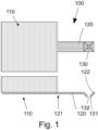
- Fig. 1 shows a probe 100 as can be manufactured using the method according to the invention in top view (top) and cross-sectional view (bottom), both views being vertically aligned.
- the probe 100 comprises a probe body section 110 and a cantilever 120.
- the cantilever 120 has a proximal end 121 connected to the probe body section 110 and a distal cantilever end 122.
- the distal cantilever end 122 comprises a pyramidal tip 130 comprising a pyramidal tip end 131 comprising a central through-hole 132.
- This probe is described in " Nanoscale dispensing of liquids through cantilevered probes" (A. Meister et al. Microelectronic Engineering 67-6° (2003) 644-650 ) and its manufacture is replicated using the method according to the present invention, as will be illustrated below.
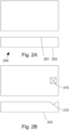
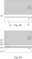
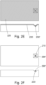
- Fig. 2A to Fig. 2K show in top view and cross-sectional view a method of manufacturing the probe 100 of Fig. 1 .
- the method according to the present invention allows for a multitude of through-holes 132 and hence probes 100 to be manufactured at once, but the figures will show one probe 100 in the making only.
- a silicon wafer 200 (a crystalline substrate, which will provide body 260) having a thickness of 380 um is shown ( Fig. 2A ) in top view.
- the silicon wafer 200 is of (1,0,C) silicon. If a pyramidal tip with three faces is desired, (1,1,1) silicon may be used instead.
- pyramidal recesses 210 (further on called pits; only one shown, singulars are used in the remainder of the figure description) is etched by wet anisotropic etching of the silicon using 25% KOH ( Fig. 2B ).
- the pyramidal pit 210 is 10 um by 10 um.
- a thin layer of first material 220 (300 nm), here silicon nitride, is deposited ( Fig. 2C ) on the silicon wafer 200 comprising a pyramidal pit 210 ( Fig. 2C ) using Low Pressure Chemical Deposition (LPCVD) so as to result in an intermediate product, having a first main side 201 and a second main side 202.
- first material 220 here silicon nitride
- the intermediate product is provided with a layer of positive photoresist (OiR 907-17 photoresist available from FujiFilm), that polymerizes so as to yield a polymerized layer of positive photoresist 290 ( Fig. 2D ). It has an outer surface 291 and an inner surface 292 adjacent to the first layer.
- a layer of positive photoresist (OiR 907-17 photoresist available from FujiFilm)
- the polymerized layer is subjected to light at the first main side 201 for a duration and with an intensity that causes depolymerization of the positive photoresist, exposing and thus depolymerizing the outer surface 291 more strongly than photoresist further from the outer surface 291, and in particular the photoresist in the bottom section of the pit 210, in accordance with physical law of the absorption of light.
- OPD 4262 developer available from FujiFilm
- relatively less strongly depolymerized positive photoresist 290' remains in the bottom section of the pit 210 ( Fig. 2E ) closest to the second main side 202.
- the silicon nitride of the first layer 220 is etched away using Reactive Ion Etching (RTE), using the remainging relatively less strongly depolymerized photoresist 290' as a mask.
- RTE Reactive Ion Etching
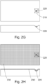
- the less strongly depolymerized positive photoresist is removed using plasma etching ( Fig. 2G ).
- the silicon of the body is oxidised (wet oxidation at 1000°C), using the silicon nitride areas as a mask ( Fig. 2H ), resulting in a wall layer 230 of silicon dioxide.
- Silicon nitride is selectively removed by wet chemical etching (hot phosphoric acid), resulting in hole 231 in the wall layer 230 ( Fig. 2I ).
- TMAH Tetramethylammonium hydroxide
- an intermediate body comprising an etched first layer exposing the substrate body material may be provided with a structural material by deposition, allowing a greater choice of structural material as it does not depend on the chemical conversion of the substrate body material.
- the structural material will have a thickness that is less than the thickness of the first layer, allowing the first layer to be etched chemically so as to form the through-hole.
Landscapes
- Engineering & Computer Science (AREA)
- Manufacturing & Machinery (AREA)
- Microelectronics & Electronic Packaging (AREA)
- Chemical & Material Sciences (AREA)
- Analytical Chemistry (AREA)
- Micromachines (AREA)
Claims (5)
- Procédé pour fournir un dispositif MEMS comprenant un trou traversant (132) dans une couche de matériau structurel (220) à l'aide d'une multitude d'étapes de procédés MEMS, dans lequel un produit intermédiaire est soumis à une pluralité d'étapes de procédés MEMS, ledit produit intermédiaire- définissant une première face principale (201) et une seconde face principale (202), et- comprenant au moins initialement un corps de substrat ayant un renfoncement (210) au niveau de la première face principale (201), ledit renfoncement (210) comprenant une section inférieure et une section supérieure relativement éloignée de la deuxième face principale (202), la section inférieure étant une section de renfoncement qui est la plus proche de la deuxième face principale (202), et la section supérieure étant une section du renfoncement (210) la plus proche de la première face principale (201) ;dans laquelle les étapes de la méthode comprennent les étapes suivantes- fournir à la première face principale (201) du substrat intermédiaire une couche polymérique de photorésine positive, ladite couche polymérique présentant une surface extérieure (291) orientée à l'opposé du corps et une surface intérieure (292) orientée vers le corps,- exposer à la lumière la couche polymère de photorésine positive dans une direction allant de la surface extérieure (291) de la photorésine positive vers le corps du substrat intermédiaire, ce qui donne une couche exposée de photorésine positive comprenant- photorésine positive relativement fortement dépolymérisée dans la section supérieure du renfoncement (210) tout en laissant- photorésine positive relativement moins fortement dépolymérisée dans la section inférieure du renfoncement (210) ;- retirer la photorésine positive relativement fortement dépolymérisée tout en laissant la photorésine positive relativement moins fortement dépolymérisée dans la section inférieure du renfoncement (210) du corps de manière à fournir une zone protégée ;- fournir un matériau structurel sur la première face principale (201) jusqu'à la zone protégée ;- graver sélectivement dans la zone protégée pour dégager le trou traversant (132) dans le matériau structurel.
- Procédé selon la revendication 1, dans lequel le corps de substrat est un substrat cristallin.
- Procédé selon la revendication 1 ou 2, dans lequel le trou traversant (132) est un trou traversant (132) dans une pointe d'un cantilever d'une sonde (100).
- Le procédé selon l'une quelconque des revendications précédentes, dans lequel le produit intermédiaire comprend- le corps (260) comprenant un matériau de corps, et- une première couche (220) d'un premier matériau (220) différent du matériau du corps au niveau de la première face principale (201) ;dans lequel- après l'étape consistant à retirer la photorésine positive relativement fortement dépolymérisée tout en laissant la photorésine positive relativement moins fortement dépolymérisée dans la section inférieure du renfoncement (210) du corps, la première couche (220) est gravée en utilisant la photorésine relativement moins fortement dépolymérisée comme masque, tout en laissant une première zone de premier matériau (220) sur le dessus du matériau du corps exposé - l'étape consistant à fournir un matériau structurel sur la première face principale (201) comprend la croissance de la couche de matériau structurel (230) par conversion du matériau du corps exposé du substrat en matériau structurel d'une composition différente du matériau du corps du substrat en utilisant au moins l'un du premier matériau restant et de la photorésine relativement moins fortement dépolymérisée en tant que masque, et- l'étape consistant à graver la zone protégée comprend en retirant ledit premier matériau restant (220).
- Procédé selon l'une quelconque des revendications précédentes, dans lequel le matériau de corps du substrat est retiré à l'emplacement du renfoncement (210) de manière à exposer le matériau structurel (230) au niveau du trou traversant (132).
Applications Claiming Priority (2)
| Application Number | Priority Date | Filing Date | Title |
|---|---|---|---|
| NL2019090A NL2019090B1 (en) | 2017-06-19 | 2017-06-19 | A method of providing a plurality of through-holes in a layer of structural material |
| PCT/NL2018/050396 WO2018236211A1 (fr) | 2017-06-19 | 2018-06-18 | Procédé de fourniture d'une pluralité de trous traversants dans une couche de matériau structural |
Publications (2)
| Publication Number | Publication Date |
|---|---|
| EP3642152A1 EP3642152A1 (fr) | 2020-04-29 |
| EP3642152B1 true EP3642152B1 (fr) | 2024-09-25 |
Family
ID=63042084
Family Applications (1)
| Application Number | Title | Priority Date | Filing Date |
|---|---|---|---|
| EP18746773.3A Active EP3642152B1 (fr) | 2017-06-19 | 2018-06-18 | Procédé de realisation d'un trou traversant dans une couche de matériau structurel |
Country Status (5)
| Country | Link |
|---|---|
| US (1) | US11174155B2 (fr) |
| EP (1) | EP3642152B1 (fr) |
| CN (1) | CN110831891B (fr) |
| NL (1) | NL2019090B1 (fr) |
| WO (1) | WO2018236211A1 (fr) |
Families Citing this family (1)
| Publication number | Priority date | Publication date | Assignee | Title |
|---|---|---|---|---|
| NL2026676B1 (en) * | 2020-10-15 | 2022-06-14 | Cytosurge Ag | A method of manufacturing a micro-fluidic probe |
Family Cites Families (8)
| Publication number | Priority date | Publication date | Assignee | Title |
|---|---|---|---|---|
| JP2869279B2 (ja) * | 1992-09-16 | 1999-03-10 | 三菱電機株式会社 | 半導体レーザダイオード及びその製造方法並びに半導体レーザダイオードアレイ |
| JP3079993B2 (ja) * | 1996-03-27 | 2000-08-21 | 日本電気株式会社 | 真空マイクロデバイスおよびその製造方法 |
| CN1599939B (zh) * | 2002-01-15 | 2010-08-11 | 国际商业机器公司 | 形成微观结构的方法 |
| US7181958B2 (en) * | 2003-12-15 | 2007-02-27 | University Of South Florida | High aspect ratio tip atomic force microscopy cantilevers and method of manufacture |
| US20070122313A1 (en) | 2005-11-30 | 2007-05-31 | Zhiyong Li | Nanochannel apparatus and method of fabricating |
| JP6164085B2 (ja) * | 2011-03-31 | 2017-07-19 | デクセリアルズ株式会社 | 光学素子、表示装置および入力装置 |
| EP3210937B1 (fr) * | 2016-02-25 | 2018-09-05 | SmartTip B.V. | Procédé de fabrication d'une pluralité de trous traversants dans une couche |
| CN106335871A (zh) * | 2016-08-30 | 2017-01-18 | 北京遥测技术研究所 | 一种硅基mems微纳通孔结构的制作方法 |
-
2017
- 2017-06-19 NL NL2019090A patent/NL2019090B1/nl active
-
2018
- 2018-06-18 CN CN201880040104.1A patent/CN110831891B/zh active Active
- 2018-06-18 EP EP18746773.3A patent/EP3642152B1/fr active Active
- 2018-06-18 US US16/619,512 patent/US11174155B2/en active Active
- 2018-06-18 WO PCT/NL2018/050396 patent/WO2018236211A1/fr not_active Ceased
Also Published As
| Publication number | Publication date |
|---|---|
| CN110831891A (zh) | 2020-02-21 |
| US11174155B2 (en) | 2021-11-16 |
| NL2019090B1 (en) | 2018-12-27 |
| WO2018236211A1 (fr) | 2018-12-27 |
| EP3642152A1 (fr) | 2020-04-29 |
| US20200165125A1 (en) | 2020-05-28 |
| CN110831891B (zh) | 2024-01-09 |
Similar Documents
| Publication | Publication Date | Title |
|---|---|---|
| DE102017112403A1 (de) | Mikroelektromechanische vorrichtung und ein verfahren zum herstellen einer mikroelektromechanischen vorrichtung | |
| WO2008046682A1 (fr) | procédé de construction d'un composant micromécanique doté d'un recouvrement en couche mince | |
| EP3642152B1 (fr) | Procédé de realisation d'un trou traversant dans une couche de matériau structurel | |
| Westerik et al. | Sidewall patterning—a new wafer-scale method for accurate patterning of vertical silicon structures | |
| CN103086321A (zh) | 一种在(111)型硅片上制作单晶硅纳米长针尖的方法 | |
| JP5078058B2 (ja) | モールド及びモールドの作製方法 | |
| US10804103B2 (en) | Microassembly of heterogeneous materials | |
| JP2010014857A (ja) | マイクロレンズモールド製造方法、マイクロレンズモールド、マイクロレンズ | |
| EP1594799A2 (fr) | Procede pour realiser un dispositif micromecanique et dispositif | |
| Tseng et al. | Sub-20 nm Si fins with high aspect ratio via pattern transfer using fullerene-based spin-on-carbon hard masks | |
| JP6305647B2 (ja) | 電気機械デバイスを製造するための方法及び対応するデバイス | |
| NL2026730B1 (en) | A method of manufacturing a MEMS device | |
| DE102016216870B4 (de) | Verfahren zum Herstellen eines mikromechanischen Bauteils mit einer freigestellten Drucksensoreinrichtung | |
| Zhang et al. | Batch fabrication of cantilever array aperture probes for scanning near-field optical microscopy | |
| DE10244785A1 (de) | Verfahren und mikromechanisches Bauelement | |
| US20140127508A1 (en) | High aspect ratio polymer elongate and one-dimensional micro structure fabrication | |
| Pinti et al. | Fabrication of Hybrid Micro-Nanofluidic Devices With Centimeter Long Ultra-Low Aspect Ratio Nanochannels | |
| Kant et al. | Suspended microstructures made using silicon migration | |
| KR102453534B1 (ko) | 미세 패턴의 제조 방법 및 이에 의해 제조된 미세 패턴 | |
| DE102012213305A1 (de) | Verfahren zur Herstellung eines MEMS-Bauelements mit einer Membranstruktur und Bauteil mit einem solchen MEMS-Bauelement | |
| JP2005014203A (ja) | マイクロデバイス及びその製造方法 | |
| KR101337568B1 (ko) | 마이크로 그리드 구조체 제조방법 | |
| Brown | Nanoscale Strain Gauges in Flexible Polymer for Biological Cell Force Measurement | |
| DE102020100244A1 (de) | Verfahren zur Herstellung eines Membran-Bauelements und ein Membran-Bauelement | |
| Lodhi et al. | Integrating 3D-Printed Metal and Polymer Geometries with CMOS Microdevices toward MEMS High-Resolution Lateral Force Sensing |
Legal Events
| Date | Code | Title | Description |
|---|---|---|---|
| STAA | Information on the status of an ep patent application or granted ep patent |
Free format text: STATUS: UNKNOWN |
|
| STAA | Information on the status of an ep patent application or granted ep patent |
Free format text: STATUS: THE INTERNATIONAL PUBLICATION HAS BEEN MADE |
|
| PUAI | Public reference made under article 153(3) epc to a published international application that has entered the european phase |
Free format text: ORIGINAL CODE: 0009012 |
|
| STAA | Information on the status of an ep patent application or granted ep patent |
Free format text: STATUS: REQUEST FOR EXAMINATION WAS MADE |
|
| 17P | Request for examination filed |
Effective date: 20191107 |
|
| AK | Designated contracting states |
Kind code of ref document: A1 Designated state(s): AL AT BE BG CH CY CZ DE DK EE ES FI FR GB GR HR HU IE IS IT LI LT LU LV MC MK MT NL NO PL PT RO RS SE SI SK SM TR |
|
| AX | Request for extension of the european patent |
Extension state: BA ME |
|
| DAV | Request for validation of the european patent (deleted) | ||
| DAX | Request for extension of the european patent (deleted) | ||
| STAA | Information on the status of an ep patent application or granted ep patent |
Free format text: STATUS: EXAMINATION IS IN PROGRESS |
|
| 17Q | First examination report despatched |
Effective date: 20210908 |
|
| GRAP | Despatch of communication of intention to grant a patent |
Free format text: ORIGINAL CODE: EPIDOSNIGR1 |
|
| STAA | Information on the status of an ep patent application or granted ep patent |
Free format text: STATUS: GRANT OF PATENT IS INTENDED |
|
| INTG | Intention to grant announced |
Effective date: 20230918 |
|
| GRAJ | Information related to disapproval of communication of intention to grant by the applicant or resumption of examination proceedings by the epo deleted |
Free format text: ORIGINAL CODE: EPIDOSDIGR1 |
|
| STAA | Information on the status of an ep patent application or granted ep patent |
Free format text: STATUS: EXAMINATION IS IN PROGRESS |
|
| INTC | Intention to grant announced (deleted) | ||
| GRAP | Despatch of communication of intention to grant a patent |
Free format text: ORIGINAL CODE: EPIDOSNIGR1 |
|
| STAA | Information on the status of an ep patent application or granted ep patent |
Free format text: STATUS: GRANT OF PATENT IS INTENDED |
|
| INTG | Intention to grant announced |
Effective date: 20240529 |
|
| GRAS | Grant fee paid |
Free format text: ORIGINAL CODE: EPIDOSNIGR3 |
|
| GRAA | (expected) grant |
Free format text: ORIGINAL CODE: 0009210 |
|
| STAA | Information on the status of an ep patent application or granted ep patent |
Free format text: STATUS: THE PATENT HAS BEEN GRANTED |
|
| AK | Designated contracting states |
Kind code of ref document: B1 Designated state(s): AL AT BE BG CH CY CZ DE DK EE ES FI FR GB GR HR HU IE IS IT LI LT LU LV MC MK MT NL NO PL PT RO RS SE SI SK SM TR |
|
| REG | Reference to a national code |
Ref country code: GB Ref legal event code: FG4D |
|
| REG | Reference to a national code |
Ref country code: CH Ref legal event code: EP |
|
| P01 | Opt-out of the competence of the unified patent court (upc) registered |
Free format text: CASE NUMBER: APP_49673/2024 Effective date: 20240902 |
|
| REG | Reference to a national code |
Ref country code: DE Ref legal event code: R096 Ref document number: 602018074707 Country of ref document: DE |
|
| REG | Reference to a national code |
Ref country code: IE Ref legal event code: FG4D |
|
| REG | Reference to a national code |
Ref country code: LT Ref legal event code: MG9D |
|
| PG25 | Lapsed in a contracting state [announced via postgrant information from national office to epo] |
Ref country code: NO Free format text: LAPSE BECAUSE OF FAILURE TO SUBMIT A TRANSLATION OF THE DESCRIPTION OR TO PAY THE FEE WITHIN THE PRESCRIBED TIME-LIMIT Effective date: 20241225 |
|
| PG25 | Lapsed in a contracting state [announced via postgrant information from national office to epo] |
Ref country code: GR Free format text: LAPSE BECAUSE OF FAILURE TO SUBMIT A TRANSLATION OF THE DESCRIPTION OR TO PAY THE FEE WITHIN THE PRESCRIBED TIME-LIMIT Effective date: 20241226 Ref country code: FI Free format text: LAPSE BECAUSE OF FAILURE TO SUBMIT A TRANSLATION OF THE DESCRIPTION OR TO PAY THE FEE WITHIN THE PRESCRIBED TIME-LIMIT Effective date: 20240925 |
|
| PG25 | Lapsed in a contracting state [announced via postgrant information from national office to epo] |
Ref country code: BG Free format text: LAPSE BECAUSE OF FAILURE TO SUBMIT A TRANSLATION OF THE DESCRIPTION OR TO PAY THE FEE WITHIN THE PRESCRIBED TIME-LIMIT Effective date: 20240925 |
|
| PG25 | Lapsed in a contracting state [announced via postgrant information from national office to epo] |
Ref country code: LV Free format text: LAPSE BECAUSE OF FAILURE TO SUBMIT A TRANSLATION OF THE DESCRIPTION OR TO PAY THE FEE WITHIN THE PRESCRIBED TIME-LIMIT Effective date: 20240925 |
|
| PG25 | Lapsed in a contracting state [announced via postgrant information from national office to epo] |
Ref country code: RS Free format text: LAPSE BECAUSE OF FAILURE TO SUBMIT A TRANSLATION OF THE DESCRIPTION OR TO PAY THE FEE WITHIN THE PRESCRIBED TIME-LIMIT Effective date: 20241225 |
|
| REG | Reference to a national code |
Ref country code: NL Ref legal event code: MP Effective date: 20240925 |
|
| PG25 | Lapsed in a contracting state [announced via postgrant information from national office to epo] |
Ref country code: RS Free format text: LAPSE BECAUSE OF FAILURE TO SUBMIT A TRANSLATION OF THE DESCRIPTION OR TO PAY THE FEE WITHIN THE PRESCRIBED TIME-LIMIT Effective date: 20241225 Ref country code: NO Free format text: LAPSE BECAUSE OF FAILURE TO SUBMIT A TRANSLATION OF THE DESCRIPTION OR TO PAY THE FEE WITHIN THE PRESCRIBED TIME-LIMIT Effective date: 20241225 Ref country code: LV Free format text: LAPSE BECAUSE OF FAILURE TO SUBMIT A TRANSLATION OF THE DESCRIPTION OR TO PAY THE FEE WITHIN THE PRESCRIBED TIME-LIMIT Effective date: 20240925 Ref country code: GR Free format text: LAPSE BECAUSE OF FAILURE TO SUBMIT A TRANSLATION OF THE DESCRIPTION OR TO PAY THE FEE WITHIN THE PRESCRIBED TIME-LIMIT Effective date: 20241226 Ref country code: FI Free format text: LAPSE BECAUSE OF FAILURE TO SUBMIT A TRANSLATION OF THE DESCRIPTION OR TO PAY THE FEE WITHIN THE PRESCRIBED TIME-LIMIT Effective date: 20240925 Ref country code: BG Free format text: LAPSE BECAUSE OF FAILURE TO SUBMIT A TRANSLATION OF THE DESCRIPTION OR TO PAY THE FEE WITHIN THE PRESCRIBED TIME-LIMIT Effective date: 20240925 |
|
| REG | Reference to a national code |
Ref country code: AT Ref legal event code: MK05 Ref document number: 1726531 Country of ref document: AT Kind code of ref document: T Effective date: 20240925 |
|
| PG25 | Lapsed in a contracting state [announced via postgrant information from national office to epo] |
Ref country code: NL Free format text: LAPSE BECAUSE OF FAILURE TO SUBMIT A TRANSLATION OF THE DESCRIPTION OR TO PAY THE FEE WITHIN THE PRESCRIBED TIME-LIMIT Effective date: 20240925 |
|
| PG25 | Lapsed in a contracting state [announced via postgrant information from national office to epo] |
Ref country code: PT Free format text: LAPSE BECAUSE OF FAILURE TO SUBMIT A TRANSLATION OF THE DESCRIPTION OR TO PAY THE FEE WITHIN THE PRESCRIBED TIME-LIMIT Effective date: 20250127 Ref country code: IS Free format text: LAPSE BECAUSE OF FAILURE TO SUBMIT A TRANSLATION OF THE DESCRIPTION OR TO PAY THE FEE WITHIN THE PRESCRIBED TIME-LIMIT Effective date: 20250125 |
|
| PG25 | Lapsed in a contracting state [announced via postgrant information from national office to epo] |
Ref country code: RO Free format text: LAPSE BECAUSE OF FAILURE TO SUBMIT A TRANSLATION OF THE DESCRIPTION OR TO PAY THE FEE WITHIN THE PRESCRIBED TIME-LIMIT Effective date: 20240925 Ref country code: SM Free format text: LAPSE BECAUSE OF FAILURE TO SUBMIT A TRANSLATION OF THE DESCRIPTION OR TO PAY THE FEE WITHIN THE PRESCRIBED TIME-LIMIT Effective date: 20240925 |
|
| PG25 | Lapsed in a contracting state [announced via postgrant information from national office to epo] |
Ref country code: ES Free format text: LAPSE BECAUSE OF FAILURE TO SUBMIT A TRANSLATION OF THE DESCRIPTION OR TO PAY THE FEE WITHIN THE PRESCRIBED TIME-LIMIT Effective date: 20240925 |
|
| PG25 | Lapsed in a contracting state [announced via postgrant information from national office to epo] |
Ref country code: EE Free format text: LAPSE BECAUSE OF FAILURE TO SUBMIT A TRANSLATION OF THE DESCRIPTION OR TO PAY THE FEE WITHIN THE PRESCRIBED TIME-LIMIT Effective date: 20240925 Ref country code: AT Free format text: LAPSE BECAUSE OF FAILURE TO SUBMIT A TRANSLATION OF THE DESCRIPTION OR TO PAY THE FEE WITHIN THE PRESCRIBED TIME-LIMIT Effective date: 20240925 |
|
| PG25 | Lapsed in a contracting state [announced via postgrant information from national office to epo] |
Ref country code: PL Free format text: LAPSE BECAUSE OF FAILURE TO SUBMIT A TRANSLATION OF THE DESCRIPTION OR TO PAY THE FEE WITHIN THE PRESCRIBED TIME-LIMIT Effective date: 20240925 Ref country code: CZ Free format text: LAPSE BECAUSE OF FAILURE TO SUBMIT A TRANSLATION OF THE DESCRIPTION OR TO PAY THE FEE WITHIN THE PRESCRIBED TIME-LIMIT Effective date: 20240925 |
|
| PG25 | Lapsed in a contracting state [announced via postgrant information from national office to epo] |
Ref country code: IT Free format text: LAPSE BECAUSE OF FAILURE TO SUBMIT A TRANSLATION OF THE DESCRIPTION OR TO PAY THE FEE WITHIN THE PRESCRIBED TIME-LIMIT Effective date: 20240925 Ref country code: SK Free format text: LAPSE BECAUSE OF FAILURE TO SUBMIT A TRANSLATION OF THE DESCRIPTION OR TO PAY THE FEE WITHIN THE PRESCRIBED TIME-LIMIT Effective date: 20240925 |
|
| REG | Reference to a national code |
Ref country code: DE Ref legal event code: R097 Ref document number: 602018074707 Country of ref document: DE |
|
| PGFP | Annual fee paid to national office [announced via postgrant information from national office to epo] |
Ref country code: DE Payment date: 20250618 Year of fee payment: 8 |
|
| PG25 | Lapsed in a contracting state [announced via postgrant information from national office to epo] |
Ref country code: DK Free format text: LAPSE BECAUSE OF FAILURE TO SUBMIT A TRANSLATION OF THE DESCRIPTION OR TO PAY THE FEE WITHIN THE PRESCRIBED TIME-LIMIT Effective date: 20240925 |
|
| PGFP | Annual fee paid to national office [announced via postgrant information from national office to epo] |
Ref country code: GB Payment date: 20250618 Year of fee payment: 8 |
|
| PGFP | Annual fee paid to national office [announced via postgrant information from national office to epo] |
Ref country code: BE Payment date: 20250618 Year of fee payment: 8 |
|
| PGFP | Annual fee paid to national office [announced via postgrant information from national office to epo] |
Ref country code: FR Payment date: 20250626 Year of fee payment: 8 |
|
| PGFP | Annual fee paid to national office [announced via postgrant information from national office to epo] |
Ref country code: IE Payment date: 20250618 Year of fee payment: 8 |
|
| PLBE | No opposition filed within time limit |
Free format text: ORIGINAL CODE: 0009261 |
|
| STAA | Information on the status of an ep patent application or granted ep patent |
Free format text: STATUS: NO OPPOSITION FILED WITHIN TIME LIMIT |
|
| REG | Reference to a national code |
Ref country code: DE Ref legal event code: R082 Ref document number: 602018074707 Country of ref document: DE Representative=s name: RENTSCH LEGAL PARTNERS GMBH, DE |
|
| 26N | No opposition filed |
Effective date: 20250626 |
|
| PG25 | Lapsed in a contracting state [announced via postgrant information from national office to epo] |
Ref country code: SE Free format text: LAPSE BECAUSE OF FAILURE TO SUBMIT A TRANSLATION OF THE DESCRIPTION OR TO PAY THE FEE WITHIN THE PRESCRIBED TIME-LIMIT Effective date: 20240925 |
|
| PGFP | Annual fee paid to national office [announced via postgrant information from national office to epo] |
Ref country code: CH Payment date: 20250701 Year of fee payment: 8 |
|
| PG25 | Lapsed in a contracting state [announced via postgrant information from national office to epo] |
Ref country code: HR Free format text: LAPSE BECAUSE OF FAILURE TO SUBMIT A TRANSLATION OF THE DESCRIPTION OR TO PAY THE FEE WITHIN THE PRESCRIBED TIME-LIMIT Effective date: 20240925 |
|
| PG25 | Lapsed in a contracting state [announced via postgrant information from national office to epo] |
Ref country code: MC Free format text: LAPSE BECAUSE OF FAILURE TO SUBMIT A TRANSLATION OF THE DESCRIPTION OR TO PAY THE FEE WITHIN THE PRESCRIBED TIME-LIMIT Effective date: 20240925 |
|
| PG25 | Lapsed in a contracting state [announced via postgrant information from national office to epo] |
Ref country code: LU Free format text: LAPSE BECAUSE OF NON-PAYMENT OF DUE FEES Effective date: 20250618 |