EP3644384A1 - Tiefe homo-emittervorrichtungsstrukturen - Google Patents
Tiefe homo-emittervorrichtungsstrukturen Download PDFInfo
- Publication number
- EP3644384A1 EP3644384A1 EP19204284.4A EP19204284A EP3644384A1 EP 3644384 A1 EP3644384 A1 EP 3644384A1 EP 19204284 A EP19204284 A EP 19204284A EP 3644384 A1 EP3644384 A1 EP 3644384A1
- Authority
- EP
- European Patent Office
- Prior art keywords
- compound
- homo
- oled
- formula
- group
- Prior art date
- Legal status (The legal status is an assumption and is not a legal conclusion. Google has not performed a legal analysis and makes no representation as to the accuracy of the status listed.)
- Pending
Links
- 0 Cc(cccc1)c1-c1ccccc1* Chemical compound Cc(cccc1)c1-c1ccccc1* 0.000 description 27
- HYQBWCRBGGYLTL-UHFFFAOYSA-N CC(CO)(C(C)(C=C)N(C)C=N)c1c(C)cc(C)cc1 Chemical compound CC(CO)(C(C)(C=C)N(C)C=N)c1c(C)cc(C)cc1 HYQBWCRBGGYLTL-UHFFFAOYSA-N 0.000 description 1
Images


Classifications
-
- H—ELECTRICITY
- H10—SEMICONDUCTOR DEVICES; ELECTRIC SOLID-STATE DEVICES NOT OTHERWISE PROVIDED FOR
- H10K—ORGANIC ELECTRIC SOLID-STATE DEVICES
- H10K50/00—Organic light-emitting devices
- H10K50/10—OLEDs or polymer light-emitting diodes [PLED]
- H10K50/11—OLEDs or polymer light-emitting diodes [PLED] characterised by the electroluminescent [EL] layers
- H10K50/12—OLEDs or polymer light-emitting diodes [PLED] characterised by the electroluminescent [EL] layers comprising dopants
-
- H—ELECTRICITY
- H10—SEMICONDUCTOR DEVICES; ELECTRIC SOLID-STATE DEVICES NOT OTHERWISE PROVIDED FOR
- H10K—ORGANIC ELECTRIC SOLID-STATE DEVICES
- H10K50/00—Organic light-emitting devices
- H10K50/10—OLEDs or polymer light-emitting diodes [PLED]
- H10K50/11—OLEDs or polymer light-emitting diodes [PLED] characterised by the electroluminescent [EL] layers
-
- C—CHEMISTRY; METALLURGY
- C09—DYES; PAINTS; POLISHES; NATURAL RESINS; ADHESIVES; COMPOSITIONS NOT OTHERWISE PROVIDED FOR; APPLICATIONS OF MATERIALS NOT OTHERWISE PROVIDED FOR
- C09K—MATERIALS FOR MISCELLANEOUS APPLICATIONS, NOT PROVIDED FOR ELSEWHERE
- C09K11/00—Luminescent materials, e.g. electroluminescent or chemiluminescent
- C09K11/06—Luminescent materials, e.g. electroluminescent or chemiluminescent containing organic luminescent materials
-
- H—ELECTRICITY
- H10—SEMICONDUCTOR DEVICES; ELECTRIC SOLID-STATE DEVICES NOT OTHERWISE PROVIDED FOR
- H10K—ORGANIC ELECTRIC SOLID-STATE DEVICES
- H10K50/00—Organic light-emitting devices
- H10K50/10—OLEDs or polymer light-emitting diodes [PLED]
-
- H—ELECTRICITY
- H10—SEMICONDUCTOR DEVICES; ELECTRIC SOLID-STATE DEVICES NOT OTHERWISE PROVIDED FOR
- H10K—ORGANIC ELECTRIC SOLID-STATE DEVICES
- H10K50/00—Organic light-emitting devices
- H10K50/10—OLEDs or polymer light-emitting diodes [PLED]
- H10K50/18—Carrier blocking layers
-
- H—ELECTRICITY
- H10—SEMICONDUCTOR DEVICES; ELECTRIC SOLID-STATE DEVICES NOT OTHERWISE PROVIDED FOR
- H10K—ORGANIC ELECTRIC SOLID-STATE DEVICES
- H10K50/00—Organic light-emitting devices
- H10K50/80—Constructional details
- H10K50/805—Electrodes
- H10K50/81—Anodes
-
- H—ELECTRICITY
- H10—SEMICONDUCTOR DEVICES; ELECTRIC SOLID-STATE DEVICES NOT OTHERWISE PROVIDED FOR
- H10K—ORGANIC ELECTRIC SOLID-STATE DEVICES
- H10K50/00—Organic light-emitting devices
- H10K50/80—Constructional details
- H10K50/805—Electrodes
- H10K50/82—Cathodes
-
- H—ELECTRICITY
- H10—SEMICONDUCTOR DEVICES; ELECTRIC SOLID-STATE DEVICES NOT OTHERWISE PROVIDED FOR
- H10K—ORGANIC ELECTRIC SOLID-STATE DEVICES
- H10K59/00—Integrated devices, or assemblies of multiple devices, comprising at least one organic light-emitting element covered by group H10K50/00
- H10K59/90—Assemblies of multiple devices comprising at least one organic light-emitting element
-
- H—ELECTRICITY
- H10—SEMICONDUCTOR DEVICES; ELECTRIC SOLID-STATE DEVICES NOT OTHERWISE PROVIDED FOR
- H10K—ORGANIC ELECTRIC SOLID-STATE DEVICES
- H10K85/00—Organic materials used in the body or electrodes of devices covered by this subclass
- H10K85/30—Coordination compounds
- H10K85/341—Transition metal complexes, e.g. Ru(II)polypyridine complexes
- H10K85/342—Transition metal complexes, e.g. Ru(II)polypyridine complexes comprising iridium
-
- H—ELECTRICITY
- H10—SEMICONDUCTOR DEVICES; ELECTRIC SOLID-STATE DEVICES NOT OTHERWISE PROVIDED FOR
- H10K—ORGANIC ELECTRIC SOLID-STATE DEVICES
- H10K85/00—Organic materials used in the body or electrodes of devices covered by this subclass
- H10K85/60—Organic compounds having low molecular weight
- H10K85/649—Aromatic compounds comprising a hetero atom
- H10K85/654—Aromatic compounds comprising a hetero atom comprising only nitrogen as heteroatom
-
- H—ELECTRICITY
- H10—SEMICONDUCTOR DEVICES; ELECTRIC SOLID-STATE DEVICES NOT OTHERWISE PROVIDED FOR
- H10K—ORGANIC ELECTRIC SOLID-STATE DEVICES
- H10K85/00—Organic materials used in the body or electrodes of devices covered by this subclass
- H10K85/60—Organic compounds having low molecular weight
- H10K85/649—Aromatic compounds comprising a hetero atom
- H10K85/657—Polycyclic condensed heteroaromatic hydrocarbons
- H10K85/6572—Polycyclic condensed heteroaromatic hydrocarbons comprising only nitrogen in the heteroaromatic polycondensed ring system, e.g. phenanthroline or carbazole
-
- H—ELECTRICITY
- H10—SEMICONDUCTOR DEVICES; ELECTRIC SOLID-STATE DEVICES NOT OTHERWISE PROVIDED FOR
- H10K—ORGANIC ELECTRIC SOLID-STATE DEVICES
- H10K85/00—Organic materials used in the body or electrodes of devices covered by this subclass
- H10K85/60—Organic compounds having low molecular weight
- H10K85/649—Aromatic compounds comprising a hetero atom
- H10K85/657—Polycyclic condensed heteroaromatic hydrocarbons
- H10K85/6574—Polycyclic condensed heteroaromatic hydrocarbons comprising only oxygen in the heteroaromatic polycondensed ring system, e.g. cumarine dyes
-
- H—ELECTRICITY
- H10—SEMICONDUCTOR DEVICES; ELECTRIC SOLID-STATE DEVICES NOT OTHERWISE PROVIDED FOR
- H10K—ORGANIC ELECTRIC SOLID-STATE DEVICES
- H10K85/00—Organic materials used in the body or electrodes of devices covered by this subclass
- H10K85/60—Organic compounds having low molecular weight
- H10K85/649—Aromatic compounds comprising a hetero atom
- H10K85/657—Polycyclic condensed heteroaromatic hydrocarbons
- H10K85/6576—Polycyclic condensed heteroaromatic hydrocarbons comprising only sulfur in the heteroaromatic polycondensed ring system, e.g. benzothiophene
-
- C—CHEMISTRY; METALLURGY
- C09—DYES; PAINTS; POLISHES; NATURAL RESINS; ADHESIVES; COMPOSITIONS NOT OTHERWISE PROVIDED FOR; APPLICATIONS OF MATERIALS NOT OTHERWISE PROVIDED FOR
- C09K—MATERIALS FOR MISCELLANEOUS APPLICATIONS, NOT PROVIDED FOR ELSEWHERE
- C09K2211/00—Chemical nature of organic luminescent or tenebrescent compounds
- C09K2211/18—Metal complexes
- C09K2211/185—Metal complexes of the platinum group, i.e. Os, Ir, Pt, Ru, Rh or Pd
-
- H—ELECTRICITY
- H10—SEMICONDUCTOR DEVICES; ELECTRIC SOLID-STATE DEVICES NOT OTHERWISE PROVIDED FOR
- H10K—ORGANIC ELECTRIC SOLID-STATE DEVICES
- H10K2101/00—Properties of the organic materials covered by group H10K85/00
- H10K2101/30—Highest occupied molecular orbital [HOMO], lowest unoccupied molecular orbital [LUMO] or Fermi energy values
-
- H—ELECTRICITY
- H10—SEMICONDUCTOR DEVICES; ELECTRIC SOLID-STATE DEVICES NOT OTHERWISE PROVIDED FOR
- H10K—ORGANIC ELECTRIC SOLID-STATE DEVICES
- H10K2101/00—Properties of the organic materials covered by group H10K85/00
- H10K2101/40—Interrelation of parameters between multiple constituent active layers or sublayers, e.g. HOMO values in adjacent layers
-
- H—ELECTRICITY
- H10—SEMICONDUCTOR DEVICES; ELECTRIC SOLID-STATE DEVICES NOT OTHERWISE PROVIDED FOR
- H10K—ORGANIC ELECTRIC SOLID-STATE DEVICES
- H10K2101/00—Properties of the organic materials covered by group H10K85/00
- H10K2101/90—Multiple hosts in the emissive layer
-
- H—ELECTRICITY
- H10—SEMICONDUCTOR DEVICES; ELECTRIC SOLID-STATE DEVICES NOT OTHERWISE PROVIDED FOR
- H10K—ORGANIC ELECTRIC SOLID-STATE DEVICES
- H10K85/00—Organic materials used in the body or electrodes of devices covered by this subclass
- H10K85/60—Organic compounds having low molecular weight
- H10K85/649—Aromatic compounds comprising a hetero atom
- H10K85/657—Polycyclic condensed heteroaromatic hydrocarbons
Definitions
- the present invention relates to compounds for use as emitters, and devices, such as organic light emitting diodes, including the same.
- Opto-electronic devices that make use of organic materials are becoming increasingly desirable for a number of reasons. Many of the materials used to make such devices are relatively inexpensive, so organic opto-electronic devices have the potential for cost advantages over inorganic devices. In addition, the inherent properties of organic materials, such as their flexibility, may make them well suited for particular applications such as fabrication on a flexible substrate. Examples of organic opto-electronic devices include organic light emitting diodes/devices (OLEDs), organic phototransistors, organic photovoltaic cells, and organic photodetectors. For OLEDs, the organic materials may have performance advantages over conventional materials. For example, the wavelength at which an organic emissive layer emits light may generally be readily tuned with appropriate dopants.
- OLEDs make use of thin organic films that emit light when voltage is applied across the device. OLEDs are becoming an increasingly interesting technology for use in applications such as flat panel displays, illumination, and backlighting. Several OLED materials and configurations are described in U.S. Pat. Nos. 5,844,363 , 6,303,238 , and 5,707,745 , which are incorporated herein by reference in their entirety.
- phosphorescent emissive molecules are full color display. Industry standards for such a display call for pixels adapted to emit particular colors, referred to as "saturated" colors. In particular, these standards call for saturated red, green, and blue pixels.
- the OLED can be designed to emit white light. In conventional liquid crystal displays emission from a white backlight is filtered using absorption filters to produce red, green and blue emission. The same technique can also be used with OLEDs.
- the white OLED can be either a single EML device or a stack structure. Color may be measured using CIE coordinates, which are well known to the art.
- organic includes polymeric materials as well as small molecule organic materials that may be used to fabricate organic opto-electronic devices.
- Small molecule refers to any organic material that is not a polymer, and "small molecules” may actually be quite large. Small molecules may include repeat units in some circumstances. For example, using a long chain alkyl group as a substituent does not remove a molecule from the "small molecule” class. Small molecules may also be incorporated into polymers, for example as a pendent group on a polymer backbone or as a part of the backbone. Small molecules may also serve as the core moiety of a dendrimer, which consists of a series of chemical shells built on the core moiety.
- the core moiety of a dendrimer may be a fluorescent or phosphorescent small molecule emitter.
- a dendrimer may be a "small molecule,” and it is believed that all dendrimers currently used in the field of OLEDs are small molecules.
- top means furthest away from the substrate, while “bottom” means closest to the substrate.
- first layer is described as “disposed over” a second layer, the first layer is disposed further away from substrate. There may be other layers between the first and second layer, unless it is specified that the first layer is "in contact with” the second layer.
- a cathode may be described as “disposed over” an anode, even though there are various organic layers in between.
- a ligand may be referred to as "photoactive” when it is believed that the ligand directly contributes to the photoactive properties of an emissive material.
- a ligand may be referred to as "ancillary” when it is believed that the ligand does not contribute to the photoactive properties of an emissive material, although an ancillary ligand may alter the properties of a photoactive ligand.
- a first "Highest Occupied Molecular Orbital” (HOMO) or “Lowest Unoccupied Molecular Orbital” (LUMO) energy level is “greater than” or "higher than” a second HOMO or LUMO energy level if the first energy level is closer to the vacuum energy level.
- IP ionization potentials
- a higher HOMO energy level corresponds to an IP having a smaller absolute value (an IP that is less negative).
- a higher LUMO energy level corresponds to an electron affinity (EA) having a smaller absolute value (an EA that is less negative).
- the LUMO energy level of a material is higher than the HOMO energy level of the same material.
- a "higher” HOMO or LUMO energy level appears closer to the top of such a diagram than a "lower” HOMO or LUMO energy level.
- a first work function is "greater than” or “higher than” a second work function if the first work function has a higher absolute value. Because work functions are generally measured as negative numbers relative to vacuum level, this means that a "higher” work function is more negative. On a conventional energy level diagram, with the vacuum level at the top, a “higher” work function is illustrated as further away from the vacuum level in the downward direction. Thus, the definitions of HOMO and LUMO energy levels follow a different convention than work functions.
- an organic light emitting diode/device is also provided.
- the OLED can include an anode, a cathode, and an organic layer, disposed between the anode and the cathode.
- the organic light emitting device is incorporated into one or more device selected from a consumer product, an electronic component module, and/or a lighting panel.
- An embodiment of the disclosed subject matter may provide an organic light emitting diode (OLED) having an anode, a cathode, an emissive layer disposed between the anode and the cathode, and a hole blocking layer disposed between the emissive and the cathode.
- the emissive layer may include a phosphorescent dopant.
- the phosphorescent dopant may have an emission in 0.5% doped PMMA (Poly(methyl methacrylate)) thin film with a peak maximum wavelength that is greater than or equal to 600 nm at room temperature.
- the energy of a highest occupied molecular orbital (HOMO) of the phosphorescent dopant may be lower than or equal to -5.1 eV, and the energy of the HOMO of the hole blocking layer may be at least 0.1 eV lower than the energy of the HOMO of the phosphorescent dopant.
- HOMO highest occupied molecular orbital
- the peak maximum wavelength of the phosphorescent dopant may be greater than or equal to 610 nm, greater than or equal to 620 nm, greater than or equal to 630 nm, greater than or equal to 650 nm, greater than or equal to 700 nm, greater than or equal to 750 nm, or greater than or equal to 800 nm.
- the OLED may have the hole blocking layer disposed on the emissive layer.
- the energy of the HOMO of the phosphorescent dopant may be lower than or equal to -5.2 eV, lower than or equal to -5.3 eV, or lower than or equal to -5.4 eV.
- the energy of the HOMO of the hole blocking layer may be at least 0.2 eV lower than the energy of the HOMO of the phosphorescent dopant, at least 0.3 eV lower than the energy of the HOMO of the phosphorescent dopant, or at least 0.4 eV lower than the energy of the HOMO of the phosphorescent dopant.
- the hole blocking layer may include the compound of Formula I, which may be one or more of: and R 1 , R 2 and R 3 each may independently represent mono to the maximum allowable substitution, or no substitution.
- R 1 , R 2 and R 3 may be independently a hydrogen or deuterium, halogen, alkyl, cycloalkyl, heteroalkyl, heterocycloalkyl, arylalkyl, alkoxy, aryloxy, amino, silyl, alkenyl, cycloalkenyl, heteroalkenyl, alkynyl, aryl, heteroaryl, acyl, carboxylic acid, ether, ester, nitrile, isonitrile, sulfanyl, sulfinyl, sulfonyl, phosphino, and/or combinations thereof.
- Each X may be independently N, CH, or CR 3 .
- Y may be O, S, Se, NAr 4 , CAr 4 Ar 5 , and SiAr 4 Ar 5 .
- Each Ar 1 -Ar 5 may be independently selected from aryl, heteroaryl, and/or a combination thereof, and L may be a direct bond or a linker comprising at least one aromatic ring.
- Each R 1 , R 2 and R 3 may be independently a hydrogen or a substituent such as aryl, heteroaryl, and/or combinations thereof.
- Each X may be independently N, or CH.
- Y may be O, S, and/or NAr 4 .
- the compound of Formula I may be the only compound in the hole blocking layer.
- the compound of Formula I may be one or more of:
- the phosphorescent dopant may emit light from a triplet excited state to a ground singlet state in the device at room temperature.
- the phosphorescent dopant may be a metal coordination complex having a metal-carbon bond.
- the metal may be Ir, Os, Pt, Pd, Ag, Au, or Cu.
- the metal coordination complex may include a ligand having a chemical moiety of pyridazine, pyrimidine, pyrazine, and/or triazine.
- the metal coordination complex may have the formula of Ir(L A ) 3, Ir(L A )(L B ) 2 , Ir(L A ) 2 (L B ), Ir(L A ) 2 (L C ), or Ir(L A )(L B )(L C ), where L A , L B , and L C are different from each other.
- the metal coordination complex may have a formula of Pt(L A )(L B ), where L A , and L B can be same or different, and where L A , and L B may be optionally connected to form a tetradentate ligand.
- the metal coordination complex may be selected from: and and
- the metal coordination complex may be a Pt complex having a tetradentate ligand.
- the tetradentate ligand may have four coordination atoms selected from: (two anionic C, two neutral N); (one anionic C, one carbene C, one neutral N, and one anionic N); (two anionic C, one carbene C, one neutral N); (one anionic C, one anionic N, two neutral N); (one anionic C, one anionic O, two neutral N); (two carbene C, two anionic N).
- the electron blocking layer may include the compound of Formula II: where R 3 , R 4 , and R 5 may each independently represent mono to the maximum allowable substitution, or no substitution, where each R 3 , R 4 , and R 5 may be independently a hydrogen or a substituent selected from deuterium, halogen, alkyl, cycloalkyl, heteroalkyl, heterocycloalkyl, arylalkyl, alkoxy, aryloxy, amino, silyl, alkenyl, cycloalkenyl, heteroalkenyl, alkynyl, aryl, heteroaryl, acyl, carboxylic acid, ether, ester, nitrile, isonitrile, sulfanyl, sulfinyl, sulfonyl, phosphino, and/or combinations thereof, and where each Ar 5 and Ar 6 may be independently selected from aryl, heteroaryl, and/or combination thereof.
- R 3 , R 4 , and R 5 may independently
- the device may be at least one type selected from: a flat panel display, a computer monitor, a medical monitor, a television, a billboard, a light for interior or exterior illumination and/or signaling, a heads-up display, a fully or partially transparent display, a flexible display, a laser printer, a telephone, a mobile phone, a tablet, a phablet, a personal digital assistant (PDA), a wearable device, a laptop computer, a digital camera, a camcorder, a viewfinder, a micro-display having an active area with a primary diagonal of 2 inches or less, a 3-D display, a virtual reality or augmented reality display, a vehicle, a video wall comprising multiple displays tiled together, a theater or stadium screen, and a sign.
- PDA personal digital assistant
- an OLED comprises at least one organic layer disposed between and electrically connected to an anode and a cathode.
- the anode injects holes and the cathode injects electrons into the organic layer(s).
- the injected holes and electrons each migrate toward the oppositely charged electrode.
- an "exciton” which is a localized electron-hole pair having an excited energy state, is formed.
- Light is emitted when the exciton relaxes via a photoemissive mechanism.
- the exciton may be localized on an excimer or an exciplex. Non-radiative mechanisms, such as thermal relaxation, may also occur, but are generally considered undesirable.
- the initial OLEDs used emissive molecules that emitted light from their singlet states ("fluorescence") as disclosed, for example, in U.S. Pat. No. 4,769,292 , which is incorporated by reference in its entirety. Fluorescent emission generally occurs in a time frame of less than 10 nanoseconds.
- FIG. 1 shows an organic light emitting device 100.
- Device 100 may include a substrate 110, an anode 115, a hole injection layer 120, a hole transport layer 125, an electron blocking layer 130, an emissive layer 135, a hole blocking layer 140, an electron transport layer 145, an electron injection layer 150, a protective layer 155, a cathode 160, and a barrier layer 170.
- Cathode 160 is a compound cathode having a first conductive layer 162 and a second conductive layer 164.
- Device 100 may be fabricated by depositing the layers described, in order. The properties and functions of these various layers, as well as example materials, are described in more detail in US 7,279,704 at cols. 6-10, which are incorporated by reference.
- each of these layers are available.
- a flexible and transparent substrate-anode combination is disclosed in U.S. Pat. No. 5,844,363 , which is incorporated by reference in its entirety.
- An example of a p-doped hole transport layer is m-MTDATA doped with F 4 -TCNQ at a molar ratio of 50:1, as disclosed in U.S. Patent Application Publication No. 2003/0230980 , which is incorporated by reference in its entirety.
- Examples of emissive and host materials are disclosed in U.S. Pat. No. 6,303,238 to Thompson et al ., which is incorporated by reference in its entirety.
- An example of an n-doped electron transport layer is BPhen doped with Li at a molar ratio of 1:1, as disclosed in U.S. Patent Application Publication No. 2003/0230980 , which is incorporated by reference in its entirety.
- U.S. Pat. Nos. 5,703,436 and 5,707,745 which are incorporated by reference in their entireties, disclose examples of cathodes including compound cathodes having a thin layer of metal such as Mg:Ag with an overlying transparent, electrically-conductive, sputter-deposited ITO layer.
- the theory and use of blocking layers is described in more detail in U.S. Pat. No. 6,097,147 and U.S. Patent Application Publication No.
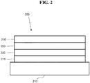
- FIG. 2 shows an inverted OLED 200.
- the device includes a substrate 210, a cathode 215, an emissive layer 220, a hole transport layer 225, and an anode 230.
- Device 200 may be fabricated by depositing the layers described, in order. Because the most common OLED configuration has a cathode disposed over the anode, and device 200 has cathode 215 disposed under anode 230, device 200 may be referred to as an "inverted" OLED. Materials similar to those described with respect to device 100 may be used in the corresponding layers of device 200.
- FIG. 2 provides one example of how some layers may be omitted from the structure of device 100.
- FIGS. 1 and 2 The simple layered structure illustrated in FIGS. 1 and 2 is provided by way of non-limiting example, and it is understood that embodiments of the invention may be used in connection with a wide variety of other structures.
- the specific materials and structures described are exemplary in nature, and other materials and structures may be used.
- Functional OLEDs may be achieved by combining the various layers described in different ways, or layers may be omitted entirely, based on design, performance, and cost factors. Other layers not specifically described may also be included. Materials other than those specifically described may be used. Although many of the examples provided herein describe various layers as comprising a single material, it is understood that combinations of materials, such as a mixture of host and dopant, or more generally a mixture, may be used. Also, the layers may have various sublayers.
- hole transport layer 225 transports holes and injects holes into emissive layer 220, and may be described as a hole transport layer or a hole injection layer.
- an OLED may be described as having an "organic layer" disposed between a cathode and an anode. This organic layer may comprise a single layer, or may further comprise multiple layers of different organic materials as described, for example, with respect to FIGS. 1 and 2 .
- OLEDs comprised of polymeric materials (PLEDs) such as disclosed in U.S. Pat. No. 5,247,190 to Friend et al. , which is incorporated by reference in its entirety.
- PLEDs polymeric materials
- OLEDs having a single organic layer may be used.
- OLEDs may be stacked, for example as described in U.S. Pat. No. 5,707,745 to Forrest et al , which is incorporated by reference in its entirety.
- the OLED structure may deviate from the simple layered structure illustrated in FIGS. 1 and 2 .
- the substrate may include an angled reflective surface to improve out-coupling, such as a mesa structure as described in U.S. Pat. No. 6,091,195 to Forrest et al. , and/or a pit structure as described in U.S. Pat. No. 5,834,893 to Bulovic et al. , which are incorporated by reference in their entireties.
- emissive layers or materials may include quantum dots.
- An "emissive layer” or “emissive material” as disclosed herein may include an organic emissive material and/or an emissive material that contains quantum dots or equivalent structures, unless indicated to the contrary explicitly or by context according to the understanding of one of skill in the art.
- Such an emissive layer may include only a quantum dot material which converts light emitted by a separate emissive material or other emitter, or it may also include the separate emissive material or other emitter, or it may emit light itself directly from the application of an electric current.
- a color altering layer, color filter, upconversion, or downconversion layer or structure may include a material containing quantum dots, though such layer may not be considered an "emissive layer" as disclosed herein.
- an "emissive layer” or material is one that emits an initial light, which may be altered by another layer such as a color filter or other color altering layer that does not itself emit an initial light within the device, but may re-emit altered light of a different spectra content based upon initial light emitted by the emissive layer.
- any of the layers of the various embodiments may be deposited by any suitable method.
- preferred methods include thermal evaporation, ink-jet, such as described in U.S. Pat. Nos. 6,013,982 and 6,087,196 , which are incorporated by reference in their entireties, organic vapor phase deposition (OVPD), such as described in U.S. Pat. No. 6,337,102 to Forrest et al. , which is incorporated by reference in its entirety, and deposition by organic vapor jet printing (OVJP), such as described in U.S. Pat. No. 7,431,968 , which is incorporated by reference in its entirety.
- OVPD organic vapor phase deposition
- OJP organic vapor jet printing
- Other suitable deposition methods include spin coating and other solution based processes.
- Solution based processes are preferably carried out in nitrogen or an inert atmosphere.
- preferred methods include thermal evaporation.
- Preferred patterning methods include deposition through a mask, cold welding such as described in U.S. Pat. Nos. 6,294,398 and 6,468,819 , which are incorporated by reference in their entireties, and patterning associated with some of the deposition methods such as ink-jet and OVJD. Other methods may also be used.
- the materials to be deposited may be modified to make them compatible with a particular deposition method. For example, substituents such as alkyl and aryl groups, branched or unbranched, and preferably containing at least 3 carbons, may be used in small molecules to enhance their ability to undergo solution processing.
- Such consumer products would include any kind of products that include one or more light source(s) and/or one or more of some type of visual displays.
- Some examples of such consumer products include flat panel displays, computer monitors, medical monitors, televisions, billboards, lights for interior or exterior illumination and/or signaling, heads-up displays, fully or partially transparent displays, flexible displays, laser printers, telephones, mobile phones, tablets, phablets, personal digital assistants (PDAs), wearable devices, laptop computers, digital cameras, camcorders, viewfinders, micro-displays (displays that are less than 2 inches diagonal), 3-D displays, virtual reality or augmented reality displays, vehicles, video walls comprising multiple displays tiled together, theater or stadium screen, and a sign.
- control mechanisms may be used to control devices fabricated in accordance with the present invention, including passive matrix and active matrix. Many of the devices are intended for use in a temperature range comfortable to humans, such as 18 C to 30 C, and more preferably at room temperature (20-25 C), but could be used outside this temperature range, for example, from -40 C to 80 C.
- the peak maximum wavelength of the phosphorescent dopant may be greater than or equal to 610 nm, greater than or equal to 620 nm, greater than or equal to 630 nm, greater than or equal to 650 nm, greater than or equal to 700 nm, greater than or equal to 750 nm, or greater than or equal to 800 nm.
- the hole blocking layer may include the compound of Formula I, which may be one or more of: and R 1 , R 2 and R 3 each may independently represent mono to the maximum allowable substitution, or no substitution.
- R 1 , R 2 and R 3 may be independently a hydrogen or deuterium, halogen, alkyl, cycloalkyl, heteroalkyl, heterocycloalkyl, arylalkyl, alkoxy, aryloxy, amino, silyl, alkenyl, cycloalkenyl, heteroalkenyl, alkynyl, aryl, heteroaryl, acyl, carboxylic acid, ether, ester, nitrile, isonitrile, sulfanyl, sulfinyl, sulfonyl, phosphino, and/or combinations thereof.
- Each X may be independently N, CH, or CR 3 .
- Y may be O, S, Se, NAr 4 , CAr 4 Ar 5 , SiAr 4 Ar 5 , Fluorene (C-Ar 1 Ar 2 ), and/or Silicon (Si-Ar 1 Ar 2 ), where Ar 1 and Ar 2 may be the same or different aryl groups.
- Each Ar 1 -Ar 5 may be independently selected from aryl, heteroaryl, and/or a combination thereof, and L may be a direct bond or a linker comprising at least one aromatic ring.
- Each R 1 , R 2 and R 3 may be independently a hydrogen or a substituent such as aryl, heteroaryl, and/or combinations thereof.
- Each X may be independently N, or CH.
- Y may be O, S, and/or NAr 4 .
- the compound of Formula I may be the only compound in the hole blocking layer.
- the compound of Formula I may be one or more of:
- the phosphorescent dopant may emit light from a triplet excited state to a ground singlet state in the device at room temperature.
- the phosphorescent dopant may be a metal coordination complex having a metal-carbon bond.
- the metal may be Ir, Os, Pt, Pd, Ag, Au, or Cu.
- the metal coordination complex may include a ligand having a chemical moiety of pyridazine, pyrimidine, pyrazine, and/or triazine.
- the metal coordination complex may have the formula of Ir(L A ) 3 , Ir(L A )(L B ) 2 , Ir(L A ) 2 (L B ), Ir(L A ) 2 (L C ), or Ir(L A )(L B )(L C ), where L A , L B , and L C are different from each other.
- the metal coordination complex may have a formula of Pt(L A )(L B ), where L A , and L B can be same or different, and where L A , and L B may be optionally connected to form a tetradentate ligand.
- the metal coordination complex may have a formula of Ir(L A ) 2 (L C ), where L A is selected from: where Lc is and where each R A , and R B may independently represent from mono substitution to the maximum possible number of substitution, or no substitution.
- Each R A , and R B may be independently selected from: hydrogen, deuterium, halogen, alkyl, cycloalkyl, heteroalkyl, heterocycloalkyl, arylalkyl, alkoxy, aryloxy, amino, silyl, alkenyl, cycloalkenyl, heteroalkenyl, alkynyl, aryl, heteroaryl, acyl, carboxylic acid, ether, ester, nitrile, isonitrile, sulfanyl, sulfinyl, sulfonyl, phosphino, and combinations thereof. Any two adjacent substituents of R A , and R B may be optionally fused or joined to form a ring or form
- the metal coordination complex may be selected from: and and
- the metal coordination complex may be a Pt complex having a tetradentate ligand.
- the tetradentate ligand may have four coordination atoms selected from: (two anionic C, two neutral N); (one anionic C, one carbene C, one neutral N, and one anionic N); (two anionic C, one carbene C, one neutral N); (one anionic C, one anionic N, two neutral N); (one anionic C, one anionic O, two neutral N); (two carbene C, two anionic N.
- the electron blocking layer may include the compound of Formula II: where R 3 , R 4 , and R 5 may each independently represent mono to the maximum allowable substitution, or no substitution, where each R 3 , R 4 , and R 5 may be independently a hydrogen or a substituent selected from deuterium, halogen, alkyl, cycloalkyl, heteroalkyl, heterocycloalkyl, arylalkyl, alkoxy, aryloxy, amino, silyl, alkenyl, cycloalkenyl, heteroalkenyl, alkynyl, aryl, heteroaryl, acyl, carboxylic acid, ether, ester, nitrile, isonitrile, sulfanyl, sulfinyl, sulfonyl, phosphino, and/or combinations thereof, and where each Ar 5 and Ar 6 may be independently selected from aryl, heteroaryl, and/or combination thereof.
- R 3 , R 4 , and R 5 may independently
- the electron blocking layer may include a compound selected from:
- the OLED has one or more characteristics selected from the group consisting of being flexible, being rollable, being foldable, being stretchable, and being curved. In some embodiments, the OLED is transparent or semi-transparent. In some embodiments, the OLED further comprises a layer comprising carbon nanotubes.
- the OLED further comprises a layer comprising a delayed fluorescent emitter.
- the OLED comprises a RGB pixel arrangement or white plus color filter pixel arrangement.
- the OLED is a mobile device, a hand held device, or a wearable device.
- the OLED is a display panel having less than 10 inch diagonal or 50 square inch area.
- the OLED is a display panel having at least 10 inch diagonal or 50 square inch area.
- the OLED is a lighting panel.
- the emissive region further comprises a host.
- the compound can be an emissive dopant.
- the compound can produce emissions via phosphorescence, fluorescence, thermally activated delayed fluorescence, i.e., TADF (also referred to as E-type delayed fluorescence), triplet-triplet annihilation, or combinations of these processes.
- TADF thermally activated delayed fluorescence
- the OLED disclosed herein can be incorporated into one or more of a consumer product, an electronic component module, and a lighting panel.
- the organic layer can be an emissive layer and the compound can be an emissive dopant in some embodiments, while the compound can be a non-emissive dopant in other embodiments.
- the organic layer can also include a host.
- a host In some embodiments, two or more hosts are preferred.
- the hosts used maybe a) bipolar, b) electron transporting, c) hole transporting or d) wide band gap materials that play little role in charge transport.
- the host can include a metal complex.
- the host can be an inorganic compound.
- a charge transport layer can be doped with conductivity dopants to substantially alter its density of charge carriers, which will in turn alter its conductivity.
- the conductivity is increased by generating charge carriers in the matrix material, and depending on the type of dopant, a change in the Fermi level of the semiconductor may also be achieved.
- Hole-transporting layer can be doped by p-type conductivity dopants and n-type conductivity dopants are used in the electron-transporting layer.
- a hole injecting/transporting material to be used in the present invention is not particularly limited, and any compound may be used as long as the compound is typically used as a hole injecting/transporting material.
- An electron blocking layer may be used to reduce the number of electrons and/or excitons that leave the emissive layer.
- the presence of such a blocking layer in a device may result in substantially higher efficiencies, and or longer lifetime, as compared to a similar device lacking a blocking layer.
- a blocking layer may be used to confine emission to a desired region of an OLED.
- the EBL material has a higher LUMO (closer to the vacuum level) and/or higher triplet energy than the emitter closest to the EBL interface.
- the EBL material has a higher LUMO (closer to the vacuum level) and or higher triplet energy than one or more of the hosts closest to the EBL interface.
- the compound used in EBL contains the same molecule or the same functional groups used as one of the hosts described below.
- the light emitting layer of the organic EL device of the present invention preferably contains at least a metal complex as light emitting material, and may contain a host material using the metal complex as a dopant material.
- the host material are not particularly limited, and any metal complexes or organic compounds may be used as long as the triplet energy of the host is larger than that of the dopant. Any host material may be used with any dopant so long as the triplet criteria is satisfied.
- a hole blocking layer may be used to reduce the number of holes and/or excitons that leave the emissive layer.
- the presence of such a blocking layer in a device may result in substantially higher efficiencies and/or longer lifetime as compared to a similar device lacking a blocking layer.
- a blocking layer may be used to confine emission to a desired region of an OLED.
- the HBL material has a lower HOMO (further from the vacuum level) and or higher triplet energy than the emitter closest to the HBL interface.
- the HBL material has a lower HOMO (further from the vacuum level) and or higher triplet energy than one or more of the hosts closest to the HBL interface.
- An electron transport layer may include a material capable of transporting electrons.
- the electron transport layer may be intrinsic (undoped), or doped. Doping may be used to enhance conductivity. Examples of the ETL material are not particularly limited, and any metal complexes or organic compounds may be used as long as they are typically used to transport electrons.
- the CGL plays an essential role in the performance, which is composed of an n-doped layer and a p-doped layer for injection of electrons and holes, respectively. Electrons and holes are supplied from the CGL and electrodes. The consumed electrons and holes in the CGL are refilled by the electrons and holes injected from the cathode and anode, respectively; then, the bipolar currents reach a steady state gradually.
- Typical CGL materials include n and p conductivity dopants used in the transport layers.
- Deep HOMO emitters may be PHOLED (phosphorescent organic light emitting diode) emitters with narrow spectrum, high LE / EQE (luminous efficacy/external quantum efficiency) ratio, long lifetime, and an EQE value above a predetermined amount.
- the narrow spectrum of the deep HOMO emitters may have full width at half maximum (FHWM) values of less than 50 nm, less than 45 nm, less than 40 nm, or the like. Due to narrow electroluminescent (EL) spectrum, the amount of photon emitting in invisible range over 670 nm may be minimized compared to conventional broad red emitters, and thus less photons losses may occur. Most of the emitted photons may be in the visible range, which may provide for higher luminance efficiency at the same EQE for the narrow EL emitters.
- FHWM full width at half maximum
- EL electroluminescent
- HOMO levels e.g., ⁇ -5.3 eV
- broad emitters e.g., ⁇ -5.1 eV
- Embodiments of the disclosed subject matter may provide a different approach for the efficient device structure architecture for deep HOMO emitters, such as for deep HOMO red emitters.
- narrow EL emitters may have deeper HOMO level (e.g., ⁇ 5.3 eV) when compared to the HOMO level for broad emitters (e.g., ⁇ 5.1 eV). This may cause different behavior of the emitter in the device, and different device structure architecture for deep HOMO emitters may be used.
- HOMO level e.g., ⁇ 5.3 eV
- broad emitters e.g., ⁇ 5.1 eV
- Embodiments of the disclosed subject matter provide designs for an efficient device structure for deep HOMO emitters.
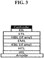
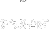
- a hole blocking layer (HBL) may affect the efficiency of deep HOMO RD1 emitter device, whereas an electron blocking layer (EBL) may not affect efficiency (e.g., as shown in examples 1, 2, 3, 4 of Table 2).
- HBL hole blocking layer
- EBL electron blocking layer
- the RD1 device may have a recombination zone close to the HBL side of EML (emissive layer).
- the HBL may improve RD1 device efficiency by preventing exciton quenching and electron leakage to the ETL (electron transport layer).
- the RD2 device may have a recombination zone (RZ) close to the EBL, and the EBL may improve device efficiency by prevention of exciton quenching and hole leakage to the HTL (hole transport layer).
- Deep HOMO RD1 may provide improved hole transport to the HBL side of EML, as there may be less hole trapping.
- the reference shallow HOMO RD2 may not provide enough hole transport through the EML, as there may be more hole trapping.
- the RZ may be localized so as to be in the proximity of EBL.
- Embodiments of the disclosed subject matter may provide for the combination of the deep HOMO emitter and HBL to provide improved device efficiency.
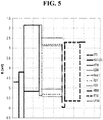
- Efficiency roll off with luminance increase may be a problem for phosphorescent devices, and reduction of efficiency roll-off may be important in order to provide increased device efficiency at higher luminances.
- EQE roll off may be calculated as ratio of EQE at 10 mA/cm 2 to EQE of 1 ma/cm 2 for the same device (see, e.g., last column in Table 2).
- Data in Table 2 and FIG. 6 shows that HBL may provide efficiency roll-off reduction for the RD1 deep HOMO emitter (see, e.g., Example 1 vs. Example 2 and Example 3 vs. Example 4 in Table 2) and may have no or minimal roll off effect on a device with an RD2 emitter (see, e.g., Example 6 vs. Example 5 and Example 7 vs. Example 8 in Table 2).
- All example devices were fabricated by high vacuum ( ⁇ 10 -7 Torr) thermal evaporation.
- the anode electrode was 1,150 ⁇ of indium tin oxide (ITO).
- the cathode was comprised of 10 ⁇ of Liq (8-hydroxyquinoline lithium) followed by 1,000 ⁇ of Al. All devices were encapsulated with a glass lid sealed with an epoxy resin in a nitrogen glove box ( ⁇ 1 ppm of H 2 O and O 2 ) immediately after fabrication, and a moisture getter was incorporated inside the package.
- HIL hole injection layer
- HTL hole transporting layer
- EBM electron blocking material
- EBL electron blocking layer
- EML an emissive layer
Landscapes
- Physics & Mathematics (AREA)
- Chemical & Material Sciences (AREA)
- Engineering & Computer Science (AREA)
- Materials Engineering (AREA)
- Optics & Photonics (AREA)
- Spectroscopy & Molecular Physics (AREA)
- Organic Chemistry (AREA)
- Crystallography & Structural Chemistry (AREA)
- Inorganic Chemistry (AREA)
- Electroluminescent Light Sources (AREA)
- Nanotechnology (AREA)
Applications Claiming Priority (2)
| Application Number | Priority Date | Filing Date | Title |
|---|---|---|---|
| US201862749290P | 2018-10-23 | 2018-10-23 | |
| US16/596,948 US11515482B2 (en) | 2018-10-23 | 2019-10-09 | Deep HOMO (highest occupied molecular orbital) emitter device structures |
Publications (1)
| Publication Number | Publication Date |
|---|---|
| EP3644384A1 true EP3644384A1 (de) | 2020-04-29 |
Family
ID=68296227
Family Applications (1)
| Application Number | Title | Priority Date | Filing Date |
|---|---|---|---|
| EP19204284.4A Pending EP3644384A1 (de) | 2018-10-23 | 2019-10-21 | Tiefe homo-emittervorrichtungsstrukturen |
Country Status (5)
| Country | Link |
|---|---|
| US (2) | US11515482B2 (de) |
| EP (1) | EP3644384A1 (de) |
| JP (2) | JP7381286B2 (de) |
| KR (2) | KR102755178B1 (de) |
| CN (3) | CN119907398A (de) |
Cited By (2)
| Publication number | Priority date | Publication date | Assignee | Title |
|---|---|---|---|---|
| EP3909964A3 (de) * | 2020-05-14 | 2022-02-16 | Samsung Electronics Co., Ltd. | Organometallische verbindung, organische lichtemittierende vorrichtung damit und elektronisches gerät mit der organischen lichtemittierenden vorrichtung |
| US12152042B2 (en) | 2020-05-14 | 2024-11-26 | Samsung Electronics Co., Ltd. | Organometallic compound, organic light-emitting device including the same, and electronic apparatus including the organic light-emitting device |
Families Citing this family (20)
| Publication number | Priority date | Publication date | Assignee | Title |
|---|---|---|---|---|
| US11217762B2 (en) * | 2018-11-30 | 2022-01-04 | Universal Display Corporation | Surface-plasmon-pumped light emitting devices |
| WO2021033724A1 (ja) | 2019-08-19 | 2021-02-25 | 出光興産株式会社 | 化合物、有機エレクトロルミネッセンス素子用材料、有機エレクトロルミネッセンス素子及び電子機器 |
| US11925105B2 (en) * | 2019-08-26 | 2024-03-05 | Universal Display Corporation | Organic electroluminescent materials and devices |
| KR20210050326A (ko) * | 2019-10-28 | 2021-05-07 | 삼성전자주식회사 | 유기금속 화합물, 이를 포함한 유기 발광 소자 및 이를 포함한 진단용 조성물 |
| CN111799385A (zh) * | 2020-07-21 | 2020-10-20 | 京东方科技集团股份有限公司 | 有机发光二极管器件及其制备方法、显示基板、显示装置 |
| CN111864095B (zh) * | 2020-07-23 | 2023-04-28 | 京东方科技集团股份有限公司 | 有机发光二极管结构、显示装置 |
| US12543492B2 (en) | 2020-09-09 | 2026-02-03 | Universal Display Corporation | Organic electroluminescent materials and devices |
| US12369488B2 (en) | 2020-09-09 | 2025-07-22 | Universal Display Corporation | Organic electroluminescent materials and devices |
| US12588352B2 (en) | 2020-10-20 | 2026-03-24 | Universal Display Corporation | Energy levels and device structures for plasmonic OLEDs |
| WO2022082764A1 (zh) * | 2020-10-23 | 2022-04-28 | 京东方科技集团股份有限公司 | 有机电致发光器件和显示装置 |
| KR102908391B1 (ko) * | 2021-02-22 | 2026-01-07 | 주식회사 엘지화학 | 신규한 화합물 및 이를 이용한 유기발광 소자 |
| JP2022128419A (ja) | 2021-02-22 | 2022-09-01 | ローム・アンド・ハース・エレクトロニック・マテリアルズ・コリア・リミテッド | 有機エレクトロルミネセント化合物、複数のホスト材料及びそれを含む有機エレクトロルミネセントデバイス |
| WO2022177398A1 (ko) * | 2021-02-22 | 2022-08-25 | 주식회사 엘지화학 | 신규한 화합물 및 이를 이용한 유기발광 소자 |
| WO2022220346A1 (ko) * | 2021-04-14 | 2022-10-20 | (주)피엔에이치테크 | 유기 화합물 및 이를 포함하는 유기발광소자 |
| US12473317B2 (en) | 2021-06-04 | 2025-11-18 | Universal Display Corporation | Organic electroluminescent materials and devices |
| CN116156984A (zh) * | 2021-11-13 | 2023-05-23 | 北京夏禾科技有限公司 | 一种有机电致发光器件 |
| EP4666820A1 (de) | 2023-02-17 | 2025-12-24 | Merck Patent GmbH | Materialien für organische elektrolumineszenzvorrichtungen |
| WO2025210013A1 (de) | 2024-04-04 | 2025-10-09 | Merck Patent Gmbh | Verbindungen für elektronische vorrichtungen, insbesondere verbindungen für oleds |
| WO2026017611A1 (en) | 2024-07-15 | 2026-01-22 | Merck Patent Gmbh | Organic light emitting device |
| CN119546049A (zh) * | 2024-11-27 | 2025-02-28 | 京东方科技集团股份有限公司 | 有机电致发光器件和显示面板 |
Citations (22)
| Publication number | Priority date | Publication date | Assignee | Title |
|---|---|---|---|---|
| US4769292A (en) | 1987-03-02 | 1988-09-06 | Eastman Kodak Company | Electroluminescent device with modified thin film luminescent zone |
| US5247190A (en) | 1989-04-20 | 1993-09-21 | Cambridge Research And Innovation Limited | Electroluminescent devices |
| US5703436A (en) | 1994-12-13 | 1997-12-30 | The Trustees Of Princeton University | Transparent contacts for organic devices |
| US5707745A (en) | 1994-12-13 | 1998-01-13 | The Trustees Of Princeton University | Multicolor organic light emitting devices |
| US5834893A (en) | 1996-12-23 | 1998-11-10 | The Trustees Of Princeton University | High efficiency organic light emitting devices with light directing structures |
| US5844363A (en) | 1997-01-23 | 1998-12-01 | The Trustees Of Princeton Univ. | Vacuum deposited, non-polymeric flexible organic light emitting devices |
| US6013982A (en) | 1996-12-23 | 2000-01-11 | The Trustees Of Princeton University | Multicolor display devices |
| US6087196A (en) | 1998-01-30 | 2000-07-11 | The Trustees Of Princeton University | Fabrication of organic semiconductor devices using ink jet printing |
| US6091195A (en) | 1997-02-03 | 2000-07-18 | The Trustees Of Princeton University | Displays having mesa pixel configuration |
| US6097147A (en) | 1998-09-14 | 2000-08-01 | The Trustees Of Princeton University | Structure for high efficiency electroluminescent device |
| US6294398B1 (en) | 1999-11-23 | 2001-09-25 | The Trustees Of Princeton University | Method for patterning devices |
| US6303238B1 (en) | 1997-12-01 | 2001-10-16 | The Trustees Of Princeton University | OLEDs doped with phosphorescent compounds |
| US6337102B1 (en) | 1997-11-17 | 2002-01-08 | The Trustees Of Princeton University | Low pressure vapor phase deposition of organic thin films |
| US20030230980A1 (en) | 2002-06-18 | 2003-12-18 | Forrest Stephen R | Very low voltage, high efficiency phosphorescent oled in a p-i-n structure |
| US20040174116A1 (en) | 2001-08-20 | 2004-09-09 | Lu Min-Hao Michael | Transparent electrodes |
| US20050112403A1 (en) * | 2003-11-25 | 2005-05-26 | Sang-Hyun Ju | Full color organic electroluminescent device |
| US7279704B2 (en) | 2004-05-18 | 2007-10-09 | The University Of Southern California | Complexes with tridentate ligands |
| US7431968B1 (en) | 2001-09-04 | 2008-10-07 | The Trustees Of Princeton University | Process and apparatus for organic vapor jet deposition |
| US20090191427A1 (en) * | 2008-01-30 | 2009-07-30 | Liang-Sheng Liao | Phosphorescent oled having double hole-blocking layers |
| US7968146B2 (en) | 2006-11-01 | 2011-06-28 | The Trustees Of Princeton University | Hybrid layers for use in coatings on electronic devices or other articles |
| US20150295197A1 (en) * | 2014-04-15 | 2015-10-15 | Universal Display Corporation | Efficient Organic Electroluminescent Devices |
| US20170229663A1 (en) | 2016-02-09 | 2017-08-10 | Universal Display Corporation | Organic electroluminescent materials and devices |
Family Cites Families (116)
| Publication number | Priority date | Publication date | Assignee | Title |
|---|---|---|---|---|
| US5061569A (en) | 1990-07-26 | 1991-10-29 | Eastman Kodak Company | Electroluminescent device with organic electroluminescent medium |
| DE69412567T2 (de) | 1993-11-01 | 1999-02-04 | Hodogaya Chemical Co., Ltd., Tokio/Tokyo | Aminverbindung und sie enthaltende Elektrolumineszenzvorrichtung |
| US6939625B2 (en) | 1996-06-25 | 2005-09-06 | Nôrthwestern University | Organic light-emitting diodes and methods for assembly and enhanced charge injection |
| US6528187B1 (en) | 1998-09-08 | 2003-03-04 | Fuji Photo Film Co., Ltd. | Material for luminescence element and luminescence element using the same |
| US6830828B2 (en) | 1998-09-14 | 2004-12-14 | The Trustees Of Princeton University | Organometallic complexes as phosphorescent emitters in organic LEDs |
| US6458475B1 (en) | 1999-11-24 | 2002-10-01 | The Trustee Of Princeton University | Organic light emitting diode having a blue phosphorescent molecule as an emitter |
| KR100377321B1 (ko) | 1999-12-31 | 2003-03-26 | 주식회사 엘지화학 | 피-형 반도체 성질을 갖는 유기 화합물을 포함하는 전기소자 |
| US20020121638A1 (en) | 2000-06-30 | 2002-09-05 | Vladimir Grushin | Electroluminescent iridium compounds with fluorinated phenylpyridines, phenylpyrimidines, and phenylquinolines and devices made with such compounds |
| JP2002050860A (ja) | 2000-08-04 | 2002-02-15 | Toray Eng Co Ltd | 実装方法および実装装置 |
| US6579630B2 (en) | 2000-12-07 | 2003-06-17 | Canon Kabushiki Kaisha | Deuterated semiconducting organic compounds used for opto-electronic devices |
| JP3812730B2 (ja) | 2001-02-01 | 2006-08-23 | 富士写真フイルム株式会社 | 遷移金属錯体及び発光素子 |
| JP4307000B2 (ja) | 2001-03-08 | 2009-08-05 | キヤノン株式会社 | 金属配位化合物、電界発光素子及び表示装置 |
| JP4310077B2 (ja) | 2001-06-19 | 2009-08-05 | キヤノン株式会社 | 金属配位化合物及び有機発光素子 |
| CN100440568C (zh) | 2001-06-20 | 2008-12-03 | 昭和电工株式会社 | 发光材料和有机发光装置 |
| US7250226B2 (en) | 2001-08-31 | 2007-07-31 | Nippon Hoso Kyokai | Phosphorescent compound, a phosphorescent composition and an organic light-emitting device |
| US6835469B2 (en) | 2001-10-17 | 2004-12-28 | The University Of Southern California | Phosphorescent compounds and devices comprising the same |
| US7166368B2 (en) | 2001-11-07 | 2007-01-23 | E. I. Du Pont De Nemours And Company | Electroluminescent platinum compounds and devices made with such compounds |
| US6863997B2 (en) | 2001-12-28 | 2005-03-08 | The Trustees Of Princeton University | White light emitting OLEDs from combined monomer and aggregate emission |
| KR100691543B1 (ko) | 2002-01-18 | 2007-03-09 | 주식회사 엘지화학 | 새로운 전자 수송용 물질 및 이를 이용한 유기 발광 소자 |
| US7189989B2 (en) | 2002-08-22 | 2007-03-13 | Fuji Photo Film Co., Ltd. | Light emitting element |
| CN100439469C (zh) | 2002-08-27 | 2008-12-03 | 富士胶片株式会社 | 有机金属配位化合物、有机el元件及有机el显示器 |
| US6687266B1 (en) | 2002-11-08 | 2004-02-03 | Universal Display Corporation | Organic light emitting materials and devices |
| JP4365196B2 (ja) | 2002-12-27 | 2009-11-18 | 富士フイルム株式会社 | 有機電界発光素子 |
| JP4365199B2 (ja) | 2002-12-27 | 2009-11-18 | 富士フイルム株式会社 | 有機電界発光素子 |
| KR101314034B1 (ko) | 2003-03-24 | 2013-10-02 | 유니버시티 오브 써던 캘리포니아 | Ir의 페닐-피라졸 착물 |
| US7090928B2 (en) | 2003-04-01 | 2006-08-15 | The University Of Southern California | Binuclear compounds |
| EP1717291A3 (de) | 2003-04-15 | 2007-03-21 | Merck Patent GmbH | Mischungen von organischen, zur Emission befähigten Halbleitern und Maxtrixmaterialien, deren Verwendung und diese Mischungen enthaltende Elektronikbauteile |
| US7029765B2 (en) | 2003-04-22 | 2006-04-18 | Universal Display Corporation | Organic light emitting devices having reduced pixel shrinkage |
| KR101032355B1 (ko) | 2003-05-29 | 2011-05-03 | 신닛테츠가가쿠 가부시키가이샤 | 유기 전계 발광 소자 |
| JP2005011610A (ja) | 2003-06-18 | 2005-01-13 | Nippon Steel Chem Co Ltd | 有機電界発光素子 |
| US20050025993A1 (en) | 2003-07-25 | 2005-02-03 | Thompson Mark E. | Materials and structures for enhancing the performance of organic light emitting devices |
| TWI390006B (zh) | 2003-08-07 | 2013-03-21 | Nippon Steel Chemical Co | Organic EL materials with aluminum clamps |
| DE10338550A1 (de) | 2003-08-19 | 2005-03-31 | Basf Ag | Übergangsmetallkomplexe mit Carbenliganden als Emitter für organische Licht-emittierende Dioden (OLEDs) |
| KR100543003B1 (ko) * | 2003-09-15 | 2006-01-20 | 삼성에스디아이 주식회사 | 풀칼라 유기 전계 발광 소자 및 그의 제조 방법 |
| US20060269780A1 (en) | 2003-09-25 | 2006-11-30 | Takayuki Fukumatsu | Organic electroluminescent device |
| JP4822687B2 (ja) | 2003-11-21 | 2011-11-24 | 富士フイルム株式会社 | 有機電界発光素子 |
| US7332232B2 (en) | 2004-02-03 | 2008-02-19 | Universal Display Corporation | OLEDs utilizing multidentate ligand systems |
| JP4992183B2 (ja) | 2004-02-10 | 2012-08-08 | 三菱化学株式会社 | 発光層形成材料及び有機電界発光素子 |
| KR100834327B1 (ko) | 2004-03-11 | 2008-06-02 | 미쓰비시 가가꾸 가부시키가이샤 | 전하 수송막용 조성물 및 이온 화합물, 이를 이용한 전하수송막 및 유기 전계 발광 장치, 및 유기 전계 발광 장치의제조 방법 및 전하 수송막의 제조 방법 |
| TW200531592A (en) | 2004-03-15 | 2005-09-16 | Nippon Steel Chemical Co | Organic electroluminescent device |
| JP4869565B2 (ja) | 2004-04-23 | 2012-02-08 | 富士フイルム株式会社 | 有機電界発光素子 |
| US7491823B2 (en) | 2004-05-18 | 2009-02-17 | The University Of Southern California | Luminescent compounds with carbene ligands |
| US7445855B2 (en) | 2004-05-18 | 2008-11-04 | The University Of Southern California | Cationic metal-carbene complexes |
| US7393599B2 (en) | 2004-05-18 | 2008-07-01 | The University Of Southern California | Luminescent compounds with carbene ligands |
| US7154114B2 (en) | 2004-05-18 | 2006-12-26 | Universal Display Corporation | Cyclometallated iridium carbene complexes for use as hosts |
| US7534505B2 (en) | 2004-05-18 | 2009-05-19 | The University Of Southern California | Organometallic compounds for use in electroluminescent devices |
| WO2005123873A1 (ja) | 2004-06-17 | 2005-12-29 | Konica Minolta Holdings, Inc. | 有機エレクトロルミネッセンス素子材料、有機エレクトロルミネッセンス素子、表示装置及び照明装置 |
| EP1893718B1 (de) | 2004-06-28 | 2018-10-03 | UDC Ireland Limited | Elektrolumineszente metallkomplexe mit triazolen und benzotriazolen |
| US20060008670A1 (en) | 2004-07-06 | 2006-01-12 | Chun Lin | Organic light emitting materials and devices |
| EP2178348B1 (de) | 2004-07-23 | 2012-11-21 | Konica Minolta Holdings, Inc. | Organisches elektrolumineszentes Element, Bildschirm und Beleuchtungseinheit |
| DE102004057072A1 (de) | 2004-11-25 | 2006-06-01 | Basf Ag | Verwendung von Übergangsmetall-Carbenkomplexen in organischen Licht-emittierenden Dioden (OLEDs) |
| JP2008526766A (ja) | 2004-12-30 | 2008-07-24 | イー・アイ・デュポン・ドウ・ヌムール・アンド・カンパニー | 有機金属錯体 |
| WO2006082742A1 (ja) | 2005-02-04 | 2006-08-10 | Konica Minolta Holdings, Inc. | 有機エレクトロルミネッセンス素子材料、有機エレクトロルミネッセンス素子、表示装置及び照明装置 |
| KR100803125B1 (ko) | 2005-03-08 | 2008-02-14 | 엘지전자 주식회사 | 적색 인광 화합물 및 이를 사용한 유기전계발광소자 |
| JP5125502B2 (ja) | 2005-03-16 | 2013-01-23 | コニカミノルタホールディングス株式会社 | 有機エレクトロルミネッセンス素子材料、有機エレクトロルミネッセンス素子 |
| DE102005014284A1 (de) | 2005-03-24 | 2006-09-28 | Basf Ag | Verwendung von Verbindungen, welche aromatische oder heteroaromatische über Carbonyl-Gruppen enthaltende Gruppen verbundene Ringe enthalten, als Matrixmaterialien in organischen Leuchtdioden |
| JPWO2006103874A1 (ja) | 2005-03-29 | 2008-09-04 | コニカミノルタホールディングス株式会社 | 有機エレクトロルミネッセンス素子材料、有機エレクトロルミネッセンス素子、表示装置及び照明装置 |
| WO2006114966A1 (ja) | 2005-04-18 | 2006-11-02 | Konica Minolta Holdings, Inc. | 有機エレクトロルミネッセンス素子、表示装置及び照明装置 |
| US7807275B2 (en) | 2005-04-21 | 2010-10-05 | Universal Display Corporation | Non-blocked phosphorescent OLEDs |
| JP4533796B2 (ja) | 2005-05-06 | 2010-09-01 | 富士フイルム株式会社 | 有機電界発光素子 |
| US9051344B2 (en) | 2005-05-06 | 2015-06-09 | Universal Display Corporation | Stability OLED materials and devices |
| US8007927B2 (en) | 2007-12-28 | 2011-08-30 | Universal Display Corporation | Dibenzothiophene-containing materials in phosphorescent light emitting diodes |
| EP2277978B1 (de) | 2005-05-31 | 2016-03-30 | Universal Display Corporation | Triphenylen wirtsmaterialien in phosphoreszierenden lichtemittierenden dioden. |
| JP4976288B2 (ja) | 2005-06-07 | 2012-07-18 | 新日鐵化学株式会社 | 有機金属錯体及びこれを用いた有機電界発光素子 |
| US7638072B2 (en) | 2005-06-27 | 2009-12-29 | E. I. Du Pont De Nemours And Company | Electrically conductive polymer compositions |
| WO2007004380A1 (ja) | 2005-07-01 | 2007-01-11 | Konica Minolta Holdings, Inc. | 有機エレクトロルミネッセンス素子材料、有機エレクトロルミネッセンス素子、表示装置及び照明装置 |
| WO2007028417A1 (en) | 2005-09-07 | 2007-03-15 | Technische Universität Braunschweig | Triplett emitter having condensed five-membered rings |
| JP4887731B2 (ja) | 2005-10-26 | 2012-02-29 | コニカミノルタホールディングス株式会社 | 有機エレクトロルミネッセンス素子、表示装置及び照明装置 |
| EP1956022B1 (de) | 2005-12-01 | 2012-07-25 | Nippon Steel Chemical Co., Ltd. | Verbindung für organisches elektrolumineszentes element und organisches elektrolumineszentes element |
| US20090295276A1 (en) | 2005-12-01 | 2009-12-03 | Tohru Asari | Organic Electroluminescent Device |
| KR102103062B1 (ko) | 2006-02-10 | 2020-04-22 | 유니버셜 디스플레이 코포레이션 | 시클로금속화 이미다조[1,2-f]페난트리딘 및 디이미다조[1,2-a:1',2'-c]퀴나졸린 리간드, 및 이의 등전자성 및 벤즈고리화된 유사체의 금속 착체 |
| JP4823730B2 (ja) | 2006-03-20 | 2011-11-24 | 新日鐵化学株式会社 | 発光層化合物及び有機電界発光素子 |
| EP2639231B1 (de) | 2006-04-26 | 2019-02-06 | Idemitsu Kosan Co., Ltd. | Aromatisches Aminderivat und organisches Elektrolumineszenzelement damit |
| JP5432523B2 (ja) | 2006-05-11 | 2014-03-05 | 出光興産株式会社 | 有機エレクトロルミネッセンス素子 |
| EP2034538B1 (de) | 2006-06-02 | 2013-10-09 | Idemitsu Kosan Co., Ltd. | Material für ein organisches elektrolumineszenzelement und das material verwendendes organisches elektrolumineszenzelement |
| KR20090040895A (ko) | 2006-08-23 | 2009-04-27 | 이데미쓰 고산 가부시키가이샤 | 방향족 아민 유도체 및 이들을 이용한 유기 전기발광 소자 |
| JP5589251B2 (ja) | 2006-09-21 | 2014-09-17 | コニカミノルタ株式会社 | 有機エレクトロルミネッセンス素子材料 |
| US20080102223A1 (en) | 2006-11-01 | 2008-05-01 | Sigurd Wagner | Hybrid layers for use in coatings on electronic devices or other articles |
| EP2080762B1 (de) | 2006-11-09 | 2016-09-14 | Nippon Steel & Sumikin Chemical Co., Ltd. | Verbindung für organische elektrolumineszenzvorrichtung und organische elektrolumineszenzvorrichtung |
| JP5133259B2 (ja) | 2006-11-24 | 2013-01-30 | 出光興産株式会社 | 芳香族アミン誘導体及びそれを用いた有機エレクトロルミネッセンス素子 |
| US8119255B2 (en) | 2006-12-08 | 2012-02-21 | Universal Display Corporation | Cross-linkable iridium complexes and organic light-emitting devices using the same |
| DE602008004738D1 (de) | 2007-02-23 | 2011-03-10 | Basf Se | Elektrolumineszente metallkomplexe mit benzotriazolen |
| CN101687893B (zh) | 2007-04-26 | 2014-01-22 | 巴斯夫欧洲公司 | 含有吩噻嗪s-氧化物或吩噻嗪s,s-二氧化物基团的硅烷及其在oled中的用途 |
| WO2008156879A1 (en) | 2007-06-20 | 2008-12-24 | Universal Display Corporation | Blue phosphorescent imidazophenanthridine materials |
| CN101720330B (zh) | 2007-06-22 | 2017-06-09 | Udc爱尔兰有限责任公司 | 发光Cu(I)络合物 |
| KR101577465B1 (ko) | 2007-07-05 | 2015-12-14 | 바스프 에스이 | 카르벤 전이 금속 착체 이미터, 및 디실릴카르바졸, 디실릴디벤조푸란, 디실릴디벤조티오펜, 디실릴디벤조포스폴, 디실릴디벤조티오펜 s-옥사이드 및 디실릴디벤조티오펜 s,s-디옥사이드로부터 선택된 1종 이상의 화합물을 포함하는 유기 발광 다이오드 |
| US20090045731A1 (en) | 2007-07-07 | 2009-02-19 | Idemitsu Kosan Co., Ltd. | Organic electroluminescence device and material for organic electroluminescence device |
| KR20100031723A (ko) | 2007-07-07 | 2010-03-24 | 이데미쓰 고산 가부시키가이샤 | 크리센 유도체 및 이를 이용한 유기 전계 발광 소자 |
| US8779655B2 (en) | 2007-07-07 | 2014-07-15 | Idemitsu Kosan Co., Ltd. | Organic electroluminescence device and material for organic electroluminescence device |
| WO2009008198A1 (ja) | 2007-07-07 | 2009-01-15 | Idemitsu Kosan Co., Ltd. | ナフタレン誘導体、有機el素子用材料及びそれを用いた有機el素子 |
| TW200909560A (en) | 2007-07-07 | 2009-03-01 | Idemitsu Kosan Co | Organic electroluminescence device and material for organic electroluminescence devcie |
| US8080658B2 (en) | 2007-07-10 | 2011-12-20 | Idemitsu Kosan Co., Ltd. | Material for organic electroluminescent element and organic electroluminescent element employing the same |
| WO2009008099A1 (ja) | 2007-07-10 | 2009-01-15 | Idemitsu Kosan Co., Ltd. | 有機エレクトロルミネッセンス素子用材料及びそれを用いた有機エレクトロルミネッセンス素子 |
| CN101688052A (zh) | 2007-07-27 | 2010-03-31 | E.I.内穆尔杜邦公司 | 包含无机纳米颗粒的导电聚合物的含水分散体 |
| CN101827834B (zh) | 2007-08-08 | 2015-11-25 | 通用显示公司 | 含苯并[9,10]菲的苯并稠合的噻吩或苯并稠合的呋喃化合物 |
| JP2009040728A (ja) | 2007-08-09 | 2009-02-26 | Canon Inc | 有機金属錯体及びこれを用いた有機発光素子 |
| EP2203461B1 (de) | 2007-10-17 | 2011-08-10 | Basf Se | Übergangsmetallkomplexe mit verbrückten carbenliganden und deren verwendung in oleds |
| US20090101870A1 (en) | 2007-10-22 | 2009-04-23 | E. I. Du Pont De Nemours And Company | Electron transport bi-layers and devices made with such bi-layers |
| US7914908B2 (en) | 2007-11-02 | 2011-03-29 | Global Oled Technology Llc | Organic electroluminescent device having an azatriphenylene derivative |
| DE102007053771A1 (de) | 2007-11-12 | 2009-05-14 | Merck Patent Gmbh | Organische Elektrolumineszenzvorrichtungen |
| EP2216313B1 (de) | 2007-11-15 | 2013-02-20 | Idemitsu Kosan Co., Ltd. | Benzochrysenderivat und organische elektrolumineszenzvorrichtung damit |
| WO2009066779A1 (ja) | 2007-11-22 | 2009-05-28 | Idemitsu Kosan Co., Ltd. | 有機el素子 |
| JP5390396B2 (ja) | 2007-11-22 | 2014-01-15 | 出光興産株式会社 | 有機el素子および有機el材料含有溶液 |
| WO2009073245A1 (en) | 2007-12-06 | 2009-06-11 | Universal Display Corporation | Light-emitting organometallic complexes |
| US8221905B2 (en) | 2007-12-28 | 2012-07-17 | Universal Display Corporation | Carbazole-containing materials in phosphorescent light emitting diodes |
| US8471248B2 (en) | 2008-02-12 | 2013-06-25 | Basf Se | Electroluminiscent metal complexes with dibenzo[f,h] quinoxalines |
| WO2010011390A2 (en) | 2008-05-07 | 2010-01-28 | The Trustees Of Princeton University | Hybrid layers for use in coatings on electronic devices or other articles |
| WO2012017751A1 (ja) | 2010-08-04 | 2012-02-09 | シャープ株式会社 | 有機発光素子、有機発光装置、および色変換方法 |
| JP5881116B2 (ja) | 2012-12-16 | 2016-03-09 | 国立大学法人信州大学 | 有機光電変換素子、および、有機薄膜太陽電池 |
| US10297762B2 (en) | 2014-07-09 | 2019-05-21 | Universal Display Corporation | Organic electroluminescent materials and devices |
| US10749113B2 (en) * | 2014-09-29 | 2020-08-18 | Universal Display Corporation | Organic electroluminescent materials and devices |
| US10361381B2 (en) * | 2015-09-03 | 2019-07-23 | Universal Display Corporation | Organic electroluminescent materials and devices |
| US10522776B2 (en) * | 2016-05-23 | 2019-12-31 | Universal Display Corporation | OLED device structures |
| US10340464B2 (en) * | 2016-11-10 | 2019-07-02 | Universal Display Corporation | Organic electroluminescent materials and devices |
| US10844085B2 (en) * | 2017-03-29 | 2020-11-24 | Universal Display Corporation | Organic electroluminescent materials and devices |
| US11276829B2 (en) * | 2017-03-31 | 2022-03-15 | Universal Display Corporation | Organic electroluminescent materials and devices |
-
2019
- 2019-10-09 US US16/596,948 patent/US11515482B2/en active Active
- 2019-10-16 JP JP2019189100A patent/JP7381286B2/ja active Active
- 2019-10-21 EP EP19204284.4A patent/EP3644384A1/de active Pending
- 2019-10-23 CN CN202510132298.XA patent/CN119907398A/zh active Pending
- 2019-10-23 CN CN201911012373.XA patent/CN111092164B/zh active Active
- 2019-10-23 CN CN202510132139.XA patent/CN119677314A/zh active Pending
- 2019-10-23 KR KR1020190132083A patent/KR102755178B1/ko active Active
-
2022
- 2022-10-25 US US17/972,727 patent/US20230108554A1/en active Pending
-
2023
- 2023-09-22 JP JP2023156586A patent/JP2023171829A/ja active Pending
-
2025
- 2025-01-09 KR KR1020250003242A patent/KR20250010736A/ko active Pending
Patent Citations (23)
| Publication number | Priority date | Publication date | Assignee | Title |
|---|---|---|---|---|
| US4769292A (en) | 1987-03-02 | 1988-09-06 | Eastman Kodak Company | Electroluminescent device with modified thin film luminescent zone |
| US5247190A (en) | 1989-04-20 | 1993-09-21 | Cambridge Research And Innovation Limited | Electroluminescent devices |
| US5703436A (en) | 1994-12-13 | 1997-12-30 | The Trustees Of Princeton University | Transparent contacts for organic devices |
| US5707745A (en) | 1994-12-13 | 1998-01-13 | The Trustees Of Princeton University | Multicolor organic light emitting devices |
| US5834893A (en) | 1996-12-23 | 1998-11-10 | The Trustees Of Princeton University | High efficiency organic light emitting devices with light directing structures |
| US6013982A (en) | 1996-12-23 | 2000-01-11 | The Trustees Of Princeton University | Multicolor display devices |
| US5844363A (en) | 1997-01-23 | 1998-12-01 | The Trustees Of Princeton Univ. | Vacuum deposited, non-polymeric flexible organic light emitting devices |
| US6091195A (en) | 1997-02-03 | 2000-07-18 | The Trustees Of Princeton University | Displays having mesa pixel configuration |
| US6337102B1 (en) | 1997-11-17 | 2002-01-08 | The Trustees Of Princeton University | Low pressure vapor phase deposition of organic thin films |
| US6303238B1 (en) | 1997-12-01 | 2001-10-16 | The Trustees Of Princeton University | OLEDs doped with phosphorescent compounds |
| US6087196A (en) | 1998-01-30 | 2000-07-11 | The Trustees Of Princeton University | Fabrication of organic semiconductor devices using ink jet printing |
| US6097147A (en) | 1998-09-14 | 2000-08-01 | The Trustees Of Princeton University | Structure for high efficiency electroluminescent device |
| US6294398B1 (en) | 1999-11-23 | 2001-09-25 | The Trustees Of Princeton University | Method for patterning devices |
| US6468819B1 (en) | 1999-11-23 | 2002-10-22 | The Trustees Of Princeton University | Method for patterning organic thin film devices using a die |
| US20040174116A1 (en) | 2001-08-20 | 2004-09-09 | Lu Min-Hao Michael | Transparent electrodes |
| US7431968B1 (en) | 2001-09-04 | 2008-10-07 | The Trustees Of Princeton University | Process and apparatus for organic vapor jet deposition |
| US20030230980A1 (en) | 2002-06-18 | 2003-12-18 | Forrest Stephen R | Very low voltage, high efficiency phosphorescent oled in a p-i-n structure |
| US20050112403A1 (en) * | 2003-11-25 | 2005-05-26 | Sang-Hyun Ju | Full color organic electroluminescent device |
| US7279704B2 (en) | 2004-05-18 | 2007-10-09 | The University Of Southern California | Complexes with tridentate ligands |
| US7968146B2 (en) | 2006-11-01 | 2011-06-28 | The Trustees Of Princeton University | Hybrid layers for use in coatings on electronic devices or other articles |
| US20090191427A1 (en) * | 2008-01-30 | 2009-07-30 | Liang-Sheng Liao | Phosphorescent oled having double hole-blocking layers |
| US20150295197A1 (en) * | 2014-04-15 | 2015-10-15 | Universal Display Corporation | Efficient Organic Electroluminescent Devices |
| US20170229663A1 (en) | 2016-02-09 | 2017-08-10 | Universal Display Corporation | Organic electroluminescent materials and devices |
Non-Patent Citations (2)
| Title |
|---|
| BALDO ET AL.: "Highly Efficient Phosphorescent Emission from Organic Electroluminescent Devices", NATURE, vol. 395, 1998, pages 151 - 154, XP001002103, DOI: 10.1038/25954 |
| BALDO ET AL.: "Very high-efficiency green organic light-emitting devices based on electrophosphorescence", APPL. PHYS. LETT., vol. 75, no. 3, 1999, pages 4 - 6, XP012023409, DOI: 10.1063/1.124258 |
Cited By (2)
| Publication number | Priority date | Publication date | Assignee | Title |
|---|---|---|---|---|
| EP3909964A3 (de) * | 2020-05-14 | 2022-02-16 | Samsung Electronics Co., Ltd. | Organometallische verbindung, organische lichtemittierende vorrichtung damit und elektronisches gerät mit der organischen lichtemittierenden vorrichtung |
| US12152042B2 (en) | 2020-05-14 | 2024-11-26 | Samsung Electronics Co., Ltd. | Organometallic compound, organic light-emitting device including the same, and electronic apparatus including the organic light-emitting device |
Also Published As
| Publication number | Publication date |
|---|---|
| JP2023171829A (ja) | 2023-12-05 |
| KR20200047376A (ko) | 2020-05-07 |
| JP7381286B2 (ja) | 2023-11-15 |
| US11515482B2 (en) | 2022-11-29 |
| CN119677314A (zh) | 2025-03-21 |
| US20200127212A1 (en) | 2020-04-23 |
| JP2020068380A (ja) | 2020-04-30 |
| US20230108554A1 (en) | 2023-04-06 |
| CN111092164B (zh) | 2025-03-11 |
| CN111092164A (zh) | 2020-05-01 |
| KR20250010736A (ko) | 2025-01-21 |
| KR102755178B1 (ko) | 2025-01-14 |
| CN119907398A (zh) | 2025-04-29 |
Similar Documents
| Publication | Publication Date | Title |
|---|---|---|
| EP3644384A1 (de) | Tiefe homo-emittervorrichtungsstrukturen | |
| US12593378B2 (en) | Organic electroluminescent materials and devices | |
| KR102376823B1 (ko) | 저휘도에서의 oled 디바이스 효율 감소 | |
| US11228010B2 (en) | Organic electroluminescent materials and devices | |
| US20230389410A1 (en) | Organic electroluminescent materials and devices | |
| US11700766B2 (en) | Host materials for electroluminescent devices | |
| US10975113B2 (en) | Organic electroluminescent materials and devices | |
| US11462697B2 (en) | Organic electroluminescent materials and devices | |
| US11145837B2 (en) | Color stable organic light emitting diode stack | |
| US12041846B2 (en) | Organic electroluminescent materials and devices | |
| EP3772118B1 (de) | Farbstabile mehrfarbige oled-vorrichtungsstrukturen | |
| US12588352B2 (en) | Energy levels and device structures for plasmonic OLEDs | |
| US20240164201A1 (en) | Organic electroluminescent materials and devices | |
| US20240099039A1 (en) | Use of singlet-triplet gap hosts for increasing stability of blue phosphorescent emission | |
| US20220352478A1 (en) | Organic eletroluminescent materials and devices | |
| US11214587B2 (en) | Organic electroluminescent materials and devices | |
| US20200295291A1 (en) | OLED WITH TRIPLET EMITTER AND EXCITED STATE LIFETIME LESS THAN 200 ns | |
| US20260101629A1 (en) | Sensitized organic light emitting device |
Legal Events
| Date | Code | Title | Description |
|---|---|---|---|
| PUAI | Public reference made under article 153(3) epc to a published international application that has entered the european phase |
Free format text: ORIGINAL CODE: 0009012 |
|
| STAA | Information on the status of an ep patent application or granted ep patent |
Free format text: STATUS: THE APPLICATION HAS BEEN PUBLISHED |
|
| AK | Designated contracting states |
Kind code of ref document: A1 Designated state(s): AL AT BE BG CH CY CZ DE DK EE ES FI FR GB GR HR HU IE IS IT LI LT LU LV MC MK MT NL NO PL PT RO RS SE SI SK SM TR |
|
| AX | Request for extension of the european patent |
Extension state: BA ME |
|
| STAA | Information on the status of an ep patent application or granted ep patent |
Free format text: STATUS: REQUEST FOR EXAMINATION WAS MADE |
|
| 17P | Request for examination filed |
Effective date: 20200929 |
|
| RBV | Designated contracting states (corrected) |
Designated state(s): AL AT BE BG CH CY CZ DE DK EE ES FI FR GB GR HR HU IE IS IT LI LT LU LV MC MK MT NL NO PL PT RO RS SE SI SK SM TR |
|
| STAA | Information on the status of an ep patent application or granted ep patent |
Free format text: STATUS: EXAMINATION IS IN PROGRESS |
|
| 17Q | First examination report despatched |
Effective date: 20220121 |
|
| RAP3 | Party data changed (applicant data changed or rights of an application transferred) |
Owner name: UNIVERSAL DISPLAY CORPORATION |
|
| REG | Reference to a national code |
Ref country code: DE Ref legal event code: R079 Free format text: PREVIOUS MAIN CLASS: H01L0051500000 Ipc: H10K0050110000 |
|
| RIC1 | Information provided on ipc code assigned before grant |
Ipc: H10K 50/18 20230101ALI20230810BHEP Ipc: H10K 50/11 20230101AFI20230810BHEP |
|
| GRAP | Despatch of communication of intention to grant a patent |
Free format text: ORIGINAL CODE: EPIDOSNIGR1 |
|
| STAA | Information on the status of an ep patent application or granted ep patent |
Free format text: STATUS: GRANT OF PATENT IS INTENDED |
|
| INTG | Intention to grant announced |
Effective date: 20231020 |
|
| GRAJ | Information related to disapproval of communication of intention to grant by the applicant or resumption of examination proceedings by the epo deleted |
Free format text: ORIGINAL CODE: EPIDOSDIGR1 |
|
| STAA | Information on the status of an ep patent application or granted ep patent |
Free format text: STATUS: EXAMINATION IS IN PROGRESS |
|
| INTC | Intention to grant announced (deleted) | ||
| GRAP | Despatch of communication of intention to grant a patent |
Free format text: ORIGINAL CODE: EPIDOSNIGR1 |
|
| STAA | Information on the status of an ep patent application or granted ep patent |
Free format text: STATUS: GRANT OF PATENT IS INTENDED |
|
| INTG | Intention to grant announced |
Effective date: 20260116 |
|
| P01 | Opt-out of the competence of the unified patent court (upc) registered |
Free format text: CASE NUMBER: UPC_APP_0003164_3644384/2026 Effective date: 20260129 |