EP3644584A1 - Structure coulissante de dispositif électronique - Google Patents
Structure coulissante de dispositif électronique Download PDFInfo
- Publication number
- EP3644584A1 EP3644584A1 EP19205399.9A EP19205399A EP3644584A1 EP 3644584 A1 EP3644584 A1 EP 3644584A1 EP 19205399 A EP19205399 A EP 19205399A EP 3644584 A1 EP3644584 A1 EP 3644584A1
- Authority
- EP
- European Patent Office
- Prior art keywords
- slide
- cover
- electronic device
- slide structure
- fixed
- Prior art date
- Legal status (The legal status is an assumption and is not a legal conclusion. Google has not performed a legal analysis and makes no representation as to the accuracy of the status listed.)
- Granted
Links
Images



Classifications
-
- H—ELECTRICITY
- H04—ELECTRIC COMMUNICATION TECHNIQUE
- H04M—TELEPHONIC COMMUNICATION
- H04M1/00—Substation equipment, e.g. for use by subscribers
- H04M1/02—Constructional features of telephone sets
- H04M1/0202—Portable telephone sets, e.g. cordless phones, mobile phones or bar type handsets
- H04M1/0206—Portable telephones comprising a plurality of mechanically joined movable body parts, e.g. hinged housings
- H04M1/0208—Portable telephones comprising a plurality of mechanically joined movable body parts, e.g. hinged housings characterized by the relative motions of the body parts
- H04M1/0235—Slidable or telescopic telephones, i.e. with a relative translation movement of the body parts; Telephones using a combination of translation and other relative motions of the body parts
-
- H—ELECTRICITY
- H04—ELECTRIC COMMUNICATION TECHNIQUE
- H04M—TELEPHONIC COMMUNICATION
- H04M1/00—Substation equipment, e.g. for use by subscribers
- H04M1/02—Constructional features of telephone sets
- H04M1/0202—Portable telephone sets, e.g. cordless phones, mobile phones or bar type handsets
- H04M1/0206—Portable telephones comprising a plurality of mechanically joined movable body parts, e.g. hinged housings
- H04M1/0208—Portable telephones comprising a plurality of mechanically joined movable body parts, e.g. hinged housings characterized by the relative motions of the body parts
- H04M1/0235—Slidable or telescopic telephones, i.e. with a relative translation movement of the body parts; Telephones using a combination of translation and other relative motions of the body parts
- H04M1/0237—Sliding mechanism with one degree of freedom
-
- G—PHYSICS
- G06—COMPUTING OR CALCULATING; COUNTING
- G06F—ELECTRIC DIGITAL DATA PROCESSING
- G06F1/00—Details not covered by groups G06F3/00 - G06F13/00 and G06F21/00
- G06F1/16—Constructional details or arrangements
- G06F1/1613—Constructional details or arrangements for portable computers
- G06F1/1615—Constructional details or arrangements for portable computers with several enclosures having relative motions, each enclosure supporting at least one I/O or computing function
- G06F1/1624—Constructional details or arrangements for portable computers with several enclosures having relative motions, each enclosure supporting at least one I/O or computing function with sliding enclosures, e.g. sliding keyboard or display
-
- H—ELECTRICITY
- H05—ELECTRIC TECHNIQUES NOT OTHERWISE PROVIDED FOR
- H05K—PRINTED CIRCUITS; CASINGS OR CONSTRUCTIONAL DETAILS OF ELECTRIC APPARATUS; MANUFACTURE OF ASSEMBLAGES OF ELECTRICAL COMPONENTS
- H05K5/00—Casings, cabinets or drawers for electric apparatus
- H05K5/0086—Casings, cabinets or drawers for electric apparatus portable, e.g. battery operated apparatus
-
- H—ELECTRICITY
- H05—ELECTRIC TECHNIQUES NOT OTHERWISE PROVIDED FOR
- H05K—PRINTED CIRCUITS; CASINGS OR CONSTRUCTIONAL DETAILS OF ELECTRIC APPARATUS; MANUFACTURE OF ASSEMBLAGES OF ELECTRICAL COMPONENTS
- H05K5/00—Casings, cabinets or drawers for electric apparatus
- H05K5/02—Details
- H05K5/03—Covers
-
- H—ELECTRICITY
- H04—ELECTRIC COMMUNICATION TECHNIQUE
- H04M—TELEPHONIC COMMUNICATION
- H04M1/00—Substation equipment, e.g. for use by subscribers
- H04M1/02—Constructional features of telephone sets
- H04M1/0202—Portable telephone sets, e.g. cordless phones, mobile phones or bar type handsets
- H04M1/026—Details of the structure or mounting of specific components
- H04M1/0262—Details of the structure or mounting of specific components for a battery compartment
-
- H—ELECTRICITY
- H04—ELECTRIC COMMUNICATION TECHNIQUE
- H04M—TELEPHONIC COMMUNICATION
- H04M1/00—Substation equipment, e.g. for use by subscribers
- H04M1/02—Constructional features of telephone sets
- H04M1/0202—Portable telephone sets, e.g. cordless phones, mobile phones or bar type handsets
- H04M1/026—Details of the structure or mounting of specific components
- H04M1/0264—Details of the structure or mounting of specific components for a camera module assembly
-
- H—ELECTRICITY
- H04—ELECTRIC COMMUNICATION TECHNIQUE
- H04M—TELEPHONIC COMMUNICATION
- H04M1/00—Substation equipment, e.g. for use by subscribers
- H04M1/02—Constructional features of telephone sets
- H04M1/0202—Portable telephone sets, e.g. cordless phones, mobile phones or bar type handsets
- H04M1/026—Details of the structure or mounting of specific components
- H04M1/0277—Details of the structure or mounting of specific components for a printed circuit board assembly
Definitions
- the present disclosure relates to the field of terminal technologies, and in particular, to a slide structure and an electronic device.
- Various embodiments of the present disclosure provide a slide structure, and an electronic device.
- a slide structure serves to affect a relative sliding movement between a first structure and a second structure of an electronic device and includes:
- the fixed member includes two side edges parallel to the sliding direction, and the first receiving space is formed between each of the side edges of the fixed member and the surface of the second cover, respectively.
- the fixed member is in a sheet shape; the fixed member is smooth on a surface away from the second cover; and the fixed member is thinner at the two side edges than at other parts so that the first receiving spaces are formed.
- the fitting member includes two cover portions mating with the two side edges; and the fitting member further includes a connection portion, and two ends of the connection portion are respectively connected with the two cover portions to form a U-shaped or H-shaped structure.
- connection portion is engaged with the fixed member to stop the sliding movement when the first structure and the second structure slide from a closed state to an open state.
- the cover portions are fixed to an edge of a preset recess in the first cover; where the cover portions partially overlap the preset recess so that the second receiving spaces are formed between the cover portions and the preset recess.
- an electronic device including:
- gaps between the first structure and the second structure at the first slide structure and the second slide structure in the thickness direction synergize with the preset length so that gaps in a thickness direction between the first structure and the second structure at two ends in a preset direction is no greater than a preset value.
- the electronic device includes a mainboard area, a battery area, and an antenna area disposed sequentially in the preset direction, the first slide structure being disposed at the battery area and the second slide structure being disposed at the mainboard area.
- a first gap between the first structure and the second structure in a thickness direction at the mainboard area is smaller than a second gap between the first structure and the second structure in the thickness direction at the battery area, a thickness of the first slide structure is no greater than the second gap, and a thickness of the second slide structure is no greater than the first gap.
- first may also be referred to as the second information without departing from the scope of the present application.
- second information may also be referred to as the first information.
- word “if' as used herein may be interpreted as "when” or “as” or “in response to a determination.”
- Layered structures for electronic devices have been proposed, in which components such as a camera module are displaced to a lower layer, so that areas in an upper layer where the components such as the camera module and the like are originally disposed may be cover with a screen to increase a screen size; and at the same time, by pushing and pulling different layers via built-in slide structures, the components such as the camera module and the like may still function properly.
- modules may have modular configurations, or are composed of discrete components, but nonetheless can be referred to as “modules” in general.
- the "components,” “modules,” “blocks,” “portions,” or “units” referred to herein may or may not be in modular forms.
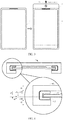
- FIG. 1 is a schematic diagram of a perspective structure of an electronic device according to an example.
- the electronic device includes a first structure 1 and a second structure 2.
- the first structure 1 may be a screen module
- the second structure 2 may be a middle frame component which contains built-in parts such as a mainboard, a battery, an antenna and the like.
- the electronic device can be divided into two parts in other ways, which is not limited herein.
- the first structure 1 and the second structure 2 are stacked along the thickness direction of the electronic device.
- the width direction of the electronic device (hereinafter also referred to as the sinistro-dextral direction) is the x-axis direction (specifically, it may be divided into a x+ direction towards the right side of the electronic device and a x-direction towards the left side of the electronic device),
- the length direction (hereinafter also referred to as the supero-inferior direction) is the y-axis direction (specifically, it may be divided into a y+direction towards the top of the electronic device and a y-direction towards the bottom of the electronic device),
- the thickness direction (hereinafter also referred to as the antero-superior direction) is the z-axis direction (specifically, it may be divided into a z+direction towards the front of the electronic device and a z-direction towards the back of the electronic device).
- first structure 1 and the second structure 2 may be substantially the same in size in the x and the y directions, so that the electronic device has a better feel of integrity. In other examples, there may be a certain difference in size between the first structure 1 and the second structure 2 due to requirements in appearance or structural design, which is not limited herein.
- the second structure 2 may have a larger size in the z direction than the first structure 1.
- the first structure 1 and the second structure 2 may be substantially the same in size in the z direction, in other words, the electronic device is equally divided into the first structure 1 and the second structure 2 in the z direction, giving itself a better visual aspect.
- size specifications of the first structure 1 and the second structure 2 in the z direction may be determined according to actual needs, which is not limited herein.
- the electronic device can be a mobile phone, a tablet computer, a personal digital assistant, etc., and can further include components such a microphone, a speaker, etc., to realize communication and multimedia functions.
- FIG. 2 is a schematic diagram of an exploded structure of the electronic device shown in FIG. 1 .
- a slide structure 4 is disposed between the first structure 1 and the second structure 2, and a relative sliding movement between the first structure 1 and the second structure 2 may be achieved based on the slide structure 4.
- FIG. 3 is a schematic diagram showing a relative sliding movement between a first structure and a second structure in the electronic device shown in FIG. 1 .
- the second structure 2 moves upward relative to the first structure 1, so that at least a portion of the surface of the second structure 2 at its upper end is exposed, where components such as a camera 20 or the like are provided.
- the first structure 1 when the first structure 1 includes a screen module, with the disposition of the camera 20 on the second structure 2, a relevant area on the first structure 1 can be spared to increase the screen-to-body ratio.
- the first structure 1 may also move downward relative to the second structure 2 to expose a corresponding part of the surface of the second structure 2, which is not limited herein.
- FIG. 4 is a schematic diagram of a slide structure in a y-axis direction.
- the slide structure includes a fixed portion 411, slide rails 412, and a slider 413.
- the top of the fixed portion 411 is fixed to the bottom surface of the first structure 1 and the bottom of the slider 413 is fixed to the top surface of the second structure 2.
- the fixed portion 411 is in a plate shape as a whole and formed with bends at both sides, and one slide rail 412 is secured to the inner sides of each bend. In this way, the slider 413 engages with the slide rails 412 on both sides to effect a sliding movement, and causes the first structure 1 and the second structure 2 to slide relative to each other.
- a thickness D along the z-axis consists of: d1 and d2, thicknesses of upper and lower portions of the fixed portion 411; d3 and d4, thicknesses of upper and lower portions of the slide rail 412; d5, a gap between the slider 413 and the upper portion of the slide rail 412; d6, a gap between the slider 413 and the lower portion of the slide rail 412; and d7, a thickness of the slider 413.
- the total thickness D of the slide structure d1 + d2 + d3 + d4 + d5 + d6 + d7.
- the total thickness D 2.7 mm.
- first structure 1 and the second structure 2 in the mainboard area are relatively close, with a gap of, for example, only 1.92 mm, which is much smaller than the above-mentioned D (2.7 mm).
- the slide structure shown in FIG. 4 is not applicable to the mainboard area of an electronic device, and if applied forcedly, it will result in an increased thickness of the electronic device, which is against the lightweight design principle.
- FIG. 5 is a schematic diagram of an exploded structure of a slide structure according to an example.
- the slide structure 3 includes a first cover 321 and a second cover 322, both of which are disposed between the first structure 1 and the second structure 2. Moreover, the first cover 321 can be fitted together with the first structure 1, and the second cover 322 can be fitted together with the second structure 2.
- the slide structure 3 may further include a fixed member 323, fixed to the second cover 322 on a surface facing the first cover 321 (that is the upper surface of the second cover 322 shown in FIG. 5 ).
- the fixed member 323 may be fixed to the second cover 322 by lock screws 324.
- Other fixing methods such as bonding and welding may also be used, which is not limited herein;
- the slide structure 3 may further include a fitting member 325, fixed to the first cover 321 on a surface facing the second cover (that is the lower surface of the first cover 321 shown in FIG. 5 ).
- the fitting member 321 may be fixed to the first cover 321 by screw locking, bonding, welding, etc., which is not limited herein.
- the fitting member 325 may cooperate with the fixed member 323 to effect a relative sliding movement between the two members, and further between the first structure 1 and the second structure 2.
- FIG. 6 is a schematic diagram of a fixed member of a slide structure and related structures thereof in a y-axis direction according to an example.
- first receiving spaces 323A and 323B are formed between the fixed member 323 and the surface of the second cover 322, with the first receiving spaces 323A and 323B extending along the relative sliding direction of the electronic device (i.e. the y-axis direction), and thus only a cross section of the first receiving spaces 323A and 323B is shown in FIG. 6 .
- the fixed member 323 may include two side edges parallel to the y-axis direction, and the fixed member 323 forms two first receiving spaces, each between one of the two side edges and the surface of the second cover 322 and represented in FIG. 6 as the first receiving space 323A on the left and the first receiving space 323B on the right, respectively.
- the first receiving spaces 323A and 323B may take various forms.
- the fixed member 323 may be in a sheet shape.
- the fixed member 323 is smooth on a surface away from the second cover 322 (i.e. the upper surface), and the fixed member 323 is thinner at the two side edges (i.e. the left and right side edges shown in FIG. 6 ) than at other parts, so that the first receiving spaces 323A and 323B as shown in FIG. 6 are formed.
- the fitting member 325 may include two corresponding cover portions 325A and 325B that extend along the above-mentioned relative sliding direction (i.e. the y-axis direction), with a right part of the cover portion 325A extending into the first receiving space 323A and a left part of the cover portion 325B extending into the first receiving space 323B, so that the cover portions 325A and 325B may engage with the first receiving spaces 323A and 323B to effect a relative sliding movement along the y-axis direction.
- the cover portions 325A and 325B may engage with the first receiving spaces 323A and 323B to effect a relative sliding movement along the y-axis direction.
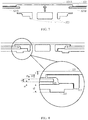
- FIG. 7 is a schematic diagram of a fitting member of a slide structure and related structures thereof in a y-axis direction according to an example.
- the fitting member 325 includes the above-mentioned cover portions 325A and 325B
- parts of the cover portions 325A and 325B may be fixed to the first cover 321 on a surface facing the second cover 322 (i.e. the lower surface in FIG.
- a left part of the cover portion 325A and a right part of the cover portion 325B are both fixed to the lower surface of the first cover 321, and second receiving spaces may be formed by other parts of the cover portions 325A and 325B and the lower surface of the first cover 321; while the cover portions 325A and 325B engage with the first receiving spaces 323A and 323B, the above-mentioned fixed member 323 may be received in the second receiving spaces and work in concert with the second receiving spaces, so that the fixed member 323 and the fitting member 325 may slide along the y-axis direction relative to each other.
- the first cover 321 includes a preset recess 321A
- the cover portions 325A and 325B may be fixed to an edge of the preset recess 321A.
- a left part of the cover portion 325A is fixed to a left edge of the preset recess 321A
- a right part of the cover portion 325B is fixed to a right edge of the preset recess 321A.
- the cover portions 325A and 325B partially overlap the preset recess, and more specifically, a right part of the cover portion 325A and a left part of the cover portion 325B partially overlap the preset recess, so that the second receiving spaces are formed therefrom.
- the second receiving spaces may be formed in other ways, for example, instead of the preset recess 321A, Z-shaped cover portions 325A and 325B are provided to form the second receiving spaces. Such detail is not limited herein.
- FIG. 8 is a schematic diagram of a slide structure in a y-axis direction according to an example.
- a thickness T along the z-axis direction consists of: t1, a thickness of the first cover 321 at the preset recess 321A; t2, a thickness of the second cover 322; t3, a thickness of the fixed member 323 at its side edges; t4, a thickness of the fitting member 325; t5, a gap between the fitting member 325 and the side edge of the fixed member 323; and t6, a gap between the fitting member 325 and the second cover 322.
- the total thickness T of the slide structure 3 t1 + t2 + t3 + t4 + t5 + t6.
- the total thickness T 1.92 mm.
- the sliding part of the slide structure has a thickness of only 0.95mm (sum of t1 + t3 + t4 + t5), which satisfies the requirement of 1.92 mm of a gap between the first structure 1 and the second structure 2. Using such a slide structure avoids an increased thickness of the electronic device and conforms to the lightweight design principle.
- FIG. 9 is a schematic diagram of a perspective view of a fitting member of a slide structure according to an example.
- the fitting member 325 when the fitting member 325 includes the cover portions 325A and 325B, the fitting member 325 may further include a connection portion 325C, and the connection portion 325C may be connected at its two ends with the two cover portions 325A and 325B to form a U-shaped structure as shown in FIG. 9 .
- an H-shaped structure or the like may be formed in other examples, which is not limited herein.
- connection portion 325C joins the cover portions 325A and 325B and makes the fitting member 325 into an integrated whole.
- cover portions 325A and 325B Compared to separately disposed cover portions 325A and 325B, such structure has better structural strength and is more stable in sliding.
- an assembly efficiency in production process is improved, with only one assembly operation for the whole structure rather than for each of the cover portions, so that a high assembly precision is maintained.
- connection portion 325C in the fitting member 325 makes it possible for the connection portion 325C to cooperate with the fixed member 323 or assist other structure to stop the sliding movement when the first structure and the second structure slide from a closed state to an open state.
- FIG. 10 is a schematic diagram showing where slide structures are disposed in an electronic device according to an example.
- the electronic device is divided into a mainboard area 11, a battery area 12, an antenna area 13, and the like in the y-axis direction; where in order to meet a clearance requirement of antenna structures, the slide structure should be avoided from being disposed in the antenna area 13.
- a gap between the first structure 1 and the second structure 2 in the thickness direction is relatively small at the mainboard area 11 and relatively large at the battery area 12, so in order to eliminate or minimize an increase of thickness in the z-axis direction of the electronic device, the slide structure 3 (as shown in FIGS. 5 to 9 ) may be disposed at the mainboard area 11 and the slide structure 4 (as shown in FIG.
- the slide structure 4 having relatively larger dimensions (one or more of length, width, thickness, etc.) and capable of bearing greater loads, may be used as a primary slide structure and the slide structure 3, having relatively smaller dimensions and capable of bearing less loads, may be used as a secondary slide structure. In this way, a relative sliding movement between the first structure and the second structure is jointly realized by the slide structure 3 and the slide structure 4 and thus becomes more stable and reliable.
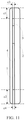
- FIG. 11 is a schematic diagram of the electronic device in FIG. 10 viewed in an x-axis direction.
- the first structure 1 and the second structure 2 are joined at the slide structure 3 and the slide structure 4. It is assumed that a distance between the slide structure 3 and a top surface of the electronic device is c1, a distance between the slide structure 4 and a bottom surface of the electronic device is c2, and a gap between the first structure and the second structure at the top surface in the thickness direction is c3 and a gap at the bottom surface is c4.
- c3 When a gap between the first structure 1 and the second structure 2 at the slide structure 3 in the thickness direction is T1, under the influence of component processing precision, assembly precision, structural stress, etc., c3 may be greater than T1, and an increase in the gap c3 is positively related to the distance c1 between the slide structure 3 and the top surface of the electronic device.
- c4 when a gap between the first structure 1 and the second structure 2 at the slide structure 4 in the thickness direction is T2, under the influence of component processing precision, assembly precision, structural stress, etc., c4 may be greater than T2, and an increase in the gap c4 is positively related to the distance c2 between the slide structure 4 and the bottom surface of the electronic device.
- the two slide structures 3 and 4 By disposing both the slide structure 3 and the slide structure 4, the two slide structures 3 and 4 as a whole affects the gaps of the electronic device at both the bottom and top ends.
- c1 the distance between the slide structure 3 and the top surface of the electronic device
- c2 the distance between the slide structure 4 and the bottom surface of the electronic device
- the gaps T1 and T2 by making the distance c1 no greater than a predefined distance threshold D1 and the distance c2 no greater than a predefined distance threshold D2, it is ensured that the gaps of the electronic device at both the bottom and top ends do not increase excessively, for example c3 and c4 are both no greater than a predefined gap threshold d0. In this way, quality control requirements are satisfied.
- the slide structures 3 and 4 may be no greater than a preset length away from edges on both sides in the width direction of the electronic device (i.e., viewed in the y-axis direction). Therefore, it is ensured that the gaps of the electronic device at the left and right surfaces also meet predefined quality control requirements. This is consistent with the example in the length direction described above and will not be described herein again.
- first and second are used for descriptive purposes only and are not to be construed as indicating or implying a relative importance or implicitly indicating the number of technical features indicated.
- elements referred to as “first” and “second” may include one or more of the features either explicitly or implicitly.
- a plurality indicates two or more unless specifically defined otherwise.
- a first element being "on” a second element may indicate direct contact between the first and second elements, without contact, or indirect geometrical relationship through one or more intermediate media or layers, unless otherwise explicitly stated and defined.
- a first element being “under,” “underneath” or “beneath” a second element may indicate direct contact between the first and second elements, without contact, or indirect geometrical relationship through one or more intermediate media or layers, unless otherwise explicitly stated and defined.
- the terms “some embodiments,” “example,” or “some examples,” and the like may indicate a specific feature described in connection with the embodiment or example, a structure, a material or feature included in at least one embodiment or example.
- the schematic representation of the above terms is not necessarily directed to the same embodiment or example.
Landscapes
- Engineering & Computer Science (AREA)
- Physics & Mathematics (AREA)
- Theoretical Computer Science (AREA)
- Signal Processing (AREA)
- Microelectronics & Electronic Packaging (AREA)
- Mathematical Physics (AREA)
- Computer Hardware Design (AREA)
- Human Computer Interaction (AREA)
- General Engineering & Computer Science (AREA)
- General Physics & Mathematics (AREA)
- Telephone Set Structure (AREA)
- Casings For Electric Apparatus (AREA)
Applications Claiming Priority (1)
| Application Number | Priority Date | Filing Date | Title |
|---|---|---|---|
| CN201811272936.4A CN111107191B (zh) | 2018-10-25 | 2018-10-25 | 滑轨结构和电子设备 |
Publications (2)
| Publication Number | Publication Date |
|---|---|
| EP3644584A1 true EP3644584A1 (fr) | 2020-04-29 |
| EP3644584B1 EP3644584B1 (fr) | 2022-08-03 |
Family
ID=68382157
Family Applications (1)
| Application Number | Title | Priority Date | Filing Date |
|---|---|---|---|
| EP19205399.9A Active EP3644584B1 (fr) | 2018-10-25 | 2019-10-25 | Structure coulissante de dispositif électronique |
Country Status (3)
| Country | Link |
|---|---|
| US (1) | US11128743B2 (fr) |
| EP (1) | EP3644584B1 (fr) |
| CN (1) | CN111107191B (fr) |
Citations (4)
| Publication number | Priority date | Publication date | Assignee | Title |
|---|---|---|---|---|
| EP1422911A2 (fr) * | 2002-11-19 | 2004-05-26 | Samsung Electronics Co., Ltd. | Terminal portable et sans fil de type coulissant |
| US20080139261A1 (en) * | 2006-12-07 | 2008-06-12 | Samsung Techwin Co., Ltd. | Magnetic levitation sliding structure |
| EP2151975A1 (fr) * | 2008-08-07 | 2010-02-10 | Hanbit Precision Co., Ltd. | Module de charnière coulissante pour téléphone mobile |
| US20120200998A1 (en) * | 2011-02-08 | 2012-08-09 | Giancarlo Anthony Giustina | Mobile computing device with moveable housing segments |
Family Cites Families (13)
| Publication number | Priority date | Publication date | Assignee | Title |
|---|---|---|---|---|
| US7520436B2 (en) * | 2005-04-18 | 2009-04-21 | Samsung Electronics Co., Ltd | Slide module for slide type portable terminal and cover apparatus for external type card mounted thereto |
| KR100697622B1 (ko) * | 2005-10-11 | 2007-03-22 | (주)브이티엘 | 슬라이딩 조립체 |
| KR100741014B1 (ko) * | 2006-07-21 | 2007-07-20 | 주식회사 엠솔버 | 휴대전화기용 슬라이딩 장치 |
| KR100762623B1 (ko) * | 2006-09-11 | 2007-10-01 | 삼성전자주식회사 | 휴대용 단말기의 슬라이딩 모듈 |
| CN101562956A (zh) * | 2008-04-18 | 2009-10-21 | 深圳富泰宏精密工业有限公司 | 滑盖机构及应用该滑盖机构的便携式电子装置 |
| CN101715280B (zh) * | 2008-10-06 | 2012-09-19 | 深圳富泰宏精密工业有限公司 | 滑盖机构及具有该滑盖机构的便携式电子装置 |
| CN101730424A (zh) * | 2008-10-10 | 2010-06-09 | 深圳富泰宏精密工业有限公司 | 滑盖机构及具有该滑盖机构的便携式电子装置 |
| JP5169945B2 (ja) * | 2009-03-30 | 2013-03-27 | 富士通株式会社 | 情報端末装置 |
| JP2011004332A (ja) * | 2009-06-22 | 2011-01-06 | Fujitsu Component Ltd | スライドヒンジ、及び携帯電子機器 |
| KR20110058975A (ko) * | 2009-11-27 | 2011-06-02 | 삼성전자주식회사 | 슬라이딩형 휴대용 단말기 |
| JP5420486B2 (ja) * | 2010-07-09 | 2014-02-19 | 三菱製鋼株式会社 | 開閉装置 |
| KR20120013800A (ko) * | 2010-08-06 | 2012-02-15 | 삼성전자주식회사 | 휴대용 통신 장치의 슬라이딩 모듈 |
| CN202282795U (zh) * | 2011-09-28 | 2012-06-20 | 比亚迪股份有限公司 | 一种滑动模组及应用其的滑盖手机 |
-
2018
- 2018-10-25 CN CN201811272936.4A patent/CN111107191B/zh active Active
-
2019
- 2019-10-22 US US16/660,723 patent/US11128743B2/en active Active
- 2019-10-25 EP EP19205399.9A patent/EP3644584B1/fr active Active
Patent Citations (4)
| Publication number | Priority date | Publication date | Assignee | Title |
|---|---|---|---|---|
| EP1422911A2 (fr) * | 2002-11-19 | 2004-05-26 | Samsung Electronics Co., Ltd. | Terminal portable et sans fil de type coulissant |
| US20080139261A1 (en) * | 2006-12-07 | 2008-06-12 | Samsung Techwin Co., Ltd. | Magnetic levitation sliding structure |
| EP2151975A1 (fr) * | 2008-08-07 | 2010-02-10 | Hanbit Precision Co., Ltd. | Module de charnière coulissante pour téléphone mobile |
| US20120200998A1 (en) * | 2011-02-08 | 2012-08-09 | Giancarlo Anthony Giustina | Mobile computing device with moveable housing segments |
Also Published As
| Publication number | Publication date |
|---|---|
| US20200137208A1 (en) | 2020-04-30 |
| CN111107191B (zh) | 2021-08-31 |
| US11128743B2 (en) | 2021-09-21 |
| EP3644584B1 (fr) | 2022-08-03 |
| CN111107191A (zh) | 2020-05-05 |
Similar Documents
| Publication | Publication Date | Title |
|---|---|---|
| CN113766771B (zh) | 包括柔性显示器的电子装置 | |
| US20170344190A1 (en) | Computer system having sensing function | |
| US20100304793A1 (en) | Mobile device having two touch screen display panels | |
| EP2579555A1 (fr) | Boîtier, ruban adhésif double-face et appareil électronique | |
| KR102345995B1 (ko) | 플렉서블 디스플레이 소자를 구비한 접철식 전자 기기 | |
| US7773374B2 (en) | Slide mechanism for slide-type portable electronic device | |
| US20100309612A1 (en) | Electronic device and sliding assembly thereof | |
| KR20180044837A (ko) | 지문 모듈을 구비한 스크린 어셈블리 및 전자 기기 | |
| CN109101115A (zh) | 键盘装置以及电子设备 | |
| US9261905B2 (en) | Electronic device | |
| CN105830140A (zh) | 折叠式设备 | |
| CN102117104A (zh) | 显示模块的组装 | |
| CN105511561A (zh) | 显示模块 | |
| US20220046811A1 (en) | Display device | |
| US9338264B2 (en) | Mobile electronic device and waterproof cover | |
| US11128743B2 (en) | Slide structure of electronic device | |
| US11079657B1 (en) | Display module | |
| US9641920B1 (en) | Support structures for computing devices | |
| US9838578B2 (en) | Frame, assembling set and camera assembly set | |
| EP3790262B1 (fr) | Dispositif électronique portable | |
| CN119889154A (zh) | 支撑件、柔性显示屏和可折叠电子设备 | |
| US11778301B2 (en) | Voice coil motor, camera module, and electronic device using the same | |
| JP7262352B2 (ja) | 板状部材の固定構造および電子機器 | |
| CN117948337A (zh) | 折叠组件、折叠装置及电子设备 | |
| EP2009972A1 (fr) | Terminal mobile |
Legal Events
| Date | Code | Title | Description |
|---|---|---|---|
| PUAI | Public reference made under article 153(3) epc to a published international application that has entered the european phase |
Free format text: ORIGINAL CODE: 0009012 |
|
| STAA | Information on the status of an ep patent application or granted ep patent |
Free format text: STATUS: THE APPLICATION HAS BEEN PUBLISHED |
|
| AK | Designated contracting states |
Kind code of ref document: A1 Designated state(s): AL AT BE BG CH CY CZ DE DK EE ES FI FR GB GR HR HU IE IS IT LI LT LU LV MC MK MT NL NO PL PT RO RS SE SI SK SM TR |
|
| AX | Request for extension of the european patent |
Extension state: BA ME |
|
| STAA | Information on the status of an ep patent application or granted ep patent |
Free format text: STATUS: REQUEST FOR EXAMINATION WAS MADE |
|
| 17P | Request for examination filed |
Effective date: 20201022 |
|
| RBV | Designated contracting states (corrected) |
Designated state(s): AL AT BE BG CH CY CZ DE DK EE ES FI FR GB GR HR HU IE IS IT LI LT LU LV MC MK MT NL NO PL PT RO RS SE SI SK SM TR |
|
| STAA | Information on the status of an ep patent application or granted ep patent |
Free format text: STATUS: EXAMINATION IS IN PROGRESS |
|
| 17Q | First examination report despatched |
Effective date: 20211011 |
|
| 17Q | First examination report despatched |
Effective date: 20211022 |
|
| GRAP | Despatch of communication of intention to grant a patent |
Free format text: ORIGINAL CODE: EPIDOSNIGR1 |
|
| STAA | Information on the status of an ep patent application or granted ep patent |
Free format text: STATUS: GRANT OF PATENT IS INTENDED |
|
| INTG | Intention to grant announced |
Effective date: 20220215 |
|
| RIN1 | Information on inventor provided before grant (corrected) |
Inventor name: SI, XINWEI |
|
| GRAS | Grant fee paid |
Free format text: ORIGINAL CODE: EPIDOSNIGR3 |
|
| GRAA | (expected) grant |
Free format text: ORIGINAL CODE: 0009210 |
|
| STAA | Information on the status of an ep patent application or granted ep patent |
Free format text: STATUS: THE PATENT HAS BEEN GRANTED |
|
| AK | Designated contracting states |
Kind code of ref document: B1 Designated state(s): AL AT BE BG CH CY CZ DE DK EE ES FI FR GB GR HR HU IE IS IT LI LT LU LV MC MK MT NL NO PL PT RO RS SE SI SK SM TR |
|
| REG | Reference to a national code |
Ref country code: AT Ref legal event code: REF Ref document number: 1509672 Country of ref document: AT Kind code of ref document: T Effective date: 20220815 Ref country code: CH Ref legal event code: EP |
|
| REG | Reference to a national code |
Ref country code: DE Ref legal event code: R096 Ref document number: 602019017713 Country of ref document: DE |
|
| REG | Reference to a national code |
Ref country code: IE Ref legal event code: FG4D |
|
| REG | Reference to a national code |
Ref country code: LT Ref legal event code: MG9D |
|
| REG | Reference to a national code |
Ref country code: NL Ref legal event code: MP Effective date: 20220803 |
|
| PG25 | Lapsed in a contracting state [announced via postgrant information from national office to epo] |
Ref country code: SE Free format text: LAPSE BECAUSE OF FAILURE TO SUBMIT A TRANSLATION OF THE DESCRIPTION OR TO PAY THE FEE WITHIN THE PRESCRIBED TIME-LIMIT Effective date: 20220803 Ref country code: RS Free format text: LAPSE BECAUSE OF FAILURE TO SUBMIT A TRANSLATION OF THE DESCRIPTION OR TO PAY THE FEE WITHIN THE PRESCRIBED TIME-LIMIT Effective date: 20220803 Ref country code: PT Free format text: LAPSE BECAUSE OF FAILURE TO SUBMIT A TRANSLATION OF THE DESCRIPTION OR TO PAY THE FEE WITHIN THE PRESCRIBED TIME-LIMIT Effective date: 20221205 Ref country code: NO Free format text: LAPSE BECAUSE OF FAILURE TO SUBMIT A TRANSLATION OF THE DESCRIPTION OR TO PAY THE FEE WITHIN THE PRESCRIBED TIME-LIMIT Effective date: 20221103 Ref country code: NL Free format text: LAPSE BECAUSE OF FAILURE TO SUBMIT A TRANSLATION OF THE DESCRIPTION OR TO PAY THE FEE WITHIN THE PRESCRIBED TIME-LIMIT Effective date: 20220803 Ref country code: LV Free format text: LAPSE BECAUSE OF FAILURE TO SUBMIT A TRANSLATION OF THE DESCRIPTION OR TO PAY THE FEE WITHIN THE PRESCRIBED TIME-LIMIT Effective date: 20220803 Ref country code: LT Free format text: LAPSE BECAUSE OF FAILURE TO SUBMIT A TRANSLATION OF THE DESCRIPTION OR TO PAY THE FEE WITHIN THE PRESCRIBED TIME-LIMIT Effective date: 20220803 Ref country code: FI Free format text: LAPSE BECAUSE OF FAILURE TO SUBMIT A TRANSLATION OF THE DESCRIPTION OR TO PAY THE FEE WITHIN THE PRESCRIBED TIME-LIMIT Effective date: 20220803 Ref country code: ES Free format text: LAPSE BECAUSE OF FAILURE TO SUBMIT A TRANSLATION OF THE DESCRIPTION OR TO PAY THE FEE WITHIN THE PRESCRIBED TIME-LIMIT Effective date: 20220803 |
|
| REG | Reference to a national code |
Ref country code: AT Ref legal event code: MK05 Ref document number: 1509672 Country of ref document: AT Kind code of ref document: T Effective date: 20220803 |
|
| PG25 | Lapsed in a contracting state [announced via postgrant information from national office to epo] |
Ref country code: PL Free format text: LAPSE BECAUSE OF FAILURE TO SUBMIT A TRANSLATION OF THE DESCRIPTION OR TO PAY THE FEE WITHIN THE PRESCRIBED TIME-LIMIT Effective date: 20220803 Ref country code: IS Free format text: LAPSE BECAUSE OF FAILURE TO SUBMIT A TRANSLATION OF THE DESCRIPTION OR TO PAY THE FEE WITHIN THE PRESCRIBED TIME-LIMIT Effective date: 20221203 Ref country code: HR Free format text: LAPSE BECAUSE OF FAILURE TO SUBMIT A TRANSLATION OF THE DESCRIPTION OR TO PAY THE FEE WITHIN THE PRESCRIBED TIME-LIMIT Effective date: 20220803 Ref country code: GR Free format text: LAPSE BECAUSE OF FAILURE TO SUBMIT A TRANSLATION OF THE DESCRIPTION OR TO PAY THE FEE WITHIN THE PRESCRIBED TIME-LIMIT Effective date: 20221104 |
|
| PG25 | Lapsed in a contracting state [announced via postgrant information from national office to epo] |
Ref country code: SM Free format text: LAPSE BECAUSE OF FAILURE TO SUBMIT A TRANSLATION OF THE DESCRIPTION OR TO PAY THE FEE WITHIN THE PRESCRIBED TIME-LIMIT Effective date: 20220803 Ref country code: RO Free format text: LAPSE BECAUSE OF FAILURE TO SUBMIT A TRANSLATION OF THE DESCRIPTION OR TO PAY THE FEE WITHIN THE PRESCRIBED TIME-LIMIT Effective date: 20220803 Ref country code: DK Free format text: LAPSE BECAUSE OF FAILURE TO SUBMIT A TRANSLATION OF THE DESCRIPTION OR TO PAY THE FEE WITHIN THE PRESCRIBED TIME-LIMIT Effective date: 20220803 Ref country code: CZ Free format text: LAPSE BECAUSE OF FAILURE TO SUBMIT A TRANSLATION OF THE DESCRIPTION OR TO PAY THE FEE WITHIN THE PRESCRIBED TIME-LIMIT Effective date: 20220803 Ref country code: AT Free format text: LAPSE BECAUSE OF FAILURE TO SUBMIT A TRANSLATION OF THE DESCRIPTION OR TO PAY THE FEE WITHIN THE PRESCRIBED TIME-LIMIT Effective date: 20220803 |
|
| REG | Reference to a national code |
Ref country code: DE Ref legal event code: R097 Ref document number: 602019017713 Country of ref document: DE |
|
| PG25 | Lapsed in a contracting state [announced via postgrant information from national office to epo] |
Ref country code: SK Free format text: LAPSE BECAUSE OF FAILURE TO SUBMIT A TRANSLATION OF THE DESCRIPTION OR TO PAY THE FEE WITHIN THE PRESCRIBED TIME-LIMIT Effective date: 20220803 Ref country code: MC Free format text: LAPSE BECAUSE OF FAILURE TO SUBMIT A TRANSLATION OF THE DESCRIPTION OR TO PAY THE FEE WITHIN THE PRESCRIBED TIME-LIMIT Effective date: 20220803 Ref country code: EE Free format text: LAPSE BECAUSE OF FAILURE TO SUBMIT A TRANSLATION OF THE DESCRIPTION OR TO PAY THE FEE WITHIN THE PRESCRIBED TIME-LIMIT Effective date: 20220803 |
|
| REG | Reference to a national code |
Ref country code: CH Ref legal event code: PL |
|
| PLBE | No opposition filed within time limit |
Free format text: ORIGINAL CODE: 0009261 |
|
| STAA | Information on the status of an ep patent application or granted ep patent |
Free format text: STATUS: NO OPPOSITION FILED WITHIN TIME LIMIT |
|
| REG | Reference to a national code |
Ref country code: BE Ref legal event code: MM Effective date: 20221031 |
|
| P01 | Opt-out of the competence of the unified patent court (upc) registered |
Effective date: 20230523 |
|
| PG25 | Lapsed in a contracting state [announced via postgrant information from national office to epo] |
Ref country code: LU Free format text: LAPSE BECAUSE OF NON-PAYMENT OF DUE FEES Effective date: 20221025 Ref country code: AL Free format text: LAPSE BECAUSE OF FAILURE TO SUBMIT A TRANSLATION OF THE DESCRIPTION OR TO PAY THE FEE WITHIN THE PRESCRIBED TIME-LIMIT Effective date: 20220803 |
|
| 26N | No opposition filed |
Effective date: 20230504 |
|
| PG25 | Lapsed in a contracting state [announced via postgrant information from national office to epo] |
Ref country code: LI Free format text: LAPSE BECAUSE OF NON-PAYMENT OF DUE FEES Effective date: 20221031 Ref country code: CH Free format text: LAPSE BECAUSE OF NON-PAYMENT OF DUE FEES Effective date: 20221031 |
|
| PG25 | Lapsed in a contracting state [announced via postgrant information from national office to epo] |
Ref country code: SI Free format text: LAPSE BECAUSE OF FAILURE TO SUBMIT A TRANSLATION OF THE DESCRIPTION OR TO PAY THE FEE WITHIN THE PRESCRIBED TIME-LIMIT Effective date: 20220803 |
|
| PG25 | Lapsed in a contracting state [announced via postgrant information from national office to epo] |
Ref country code: BE Free format text: LAPSE BECAUSE OF NON-PAYMENT OF DUE FEES Effective date: 20221031 |
|
| PG25 | Lapsed in a contracting state [announced via postgrant information from national office to epo] |
Ref country code: IE Free format text: LAPSE BECAUSE OF NON-PAYMENT OF DUE FEES Effective date: 20221025 |
|
| PG25 | Lapsed in a contracting state [announced via postgrant information from national office to epo] |
Ref country code: HU Free format text: LAPSE BECAUSE OF FAILURE TO SUBMIT A TRANSLATION OF THE DESCRIPTION OR TO PAY THE FEE WITHIN THE PRESCRIBED TIME-LIMIT; INVALID AB INITIO Effective date: 20191025 |
|
| PG25 | Lapsed in a contracting state [announced via postgrant information from national office to epo] |
Ref country code: CY Free format text: LAPSE BECAUSE OF FAILURE TO SUBMIT A TRANSLATION OF THE DESCRIPTION OR TO PAY THE FEE WITHIN THE PRESCRIBED TIME-LIMIT Effective date: 20220803 |
|
| PG25 | Lapsed in a contracting state [announced via postgrant information from national office to epo] |
Ref country code: MK Free format text: LAPSE BECAUSE OF FAILURE TO SUBMIT A TRANSLATION OF THE DESCRIPTION OR TO PAY THE FEE WITHIN THE PRESCRIBED TIME-LIMIT Effective date: 20220803 Ref country code: IT Free format text: LAPSE BECAUSE OF FAILURE TO SUBMIT A TRANSLATION OF THE DESCRIPTION OR TO PAY THE FEE WITHIN THE PRESCRIBED TIME-LIMIT Effective date: 20220803 |
|
| PG25 | Lapsed in a contracting state [announced via postgrant information from national office to epo] |
Ref country code: TR Free format text: LAPSE BECAUSE OF FAILURE TO SUBMIT A TRANSLATION OF THE DESCRIPTION OR TO PAY THE FEE WITHIN THE PRESCRIBED TIME-LIMIT Effective date: 20220803 |
|
| PG25 | Lapsed in a contracting state [announced via postgrant information from national office to epo] |
Ref country code: BG Free format text: LAPSE BECAUSE OF FAILURE TO SUBMIT A TRANSLATION OF THE DESCRIPTION OR TO PAY THE FEE WITHIN THE PRESCRIBED TIME-LIMIT Effective date: 20220803 |
|
| PG25 | Lapsed in a contracting state [announced via postgrant information from national office to epo] |
Ref country code: MT Free format text: LAPSE BECAUSE OF FAILURE TO SUBMIT A TRANSLATION OF THE DESCRIPTION OR TO PAY THE FEE WITHIN THE PRESCRIBED TIME-LIMIT Effective date: 20220803 |
|
| PGFP | Annual fee paid to national office [announced via postgrant information from national office to epo] |
Ref country code: GB Payment date: 20241025 Year of fee payment: 6 |
|
| PGFP | Annual fee paid to national office [announced via postgrant information from national office to epo] |
Ref country code: FR Payment date: 20241030 Year of fee payment: 6 |
|
| PGFP | Annual fee paid to national office [announced via postgrant information from national office to epo] |
Ref country code: DE Payment date: 20251021 Year of fee payment: 7 |