EP3647920A1 - Appareil d'affichage tactile - Google Patents
Appareil d'affichage tactile Download PDFInfo
- Publication number
- EP3647920A1 EP3647920A1 EP19205639.8A EP19205639A EP3647920A1 EP 3647920 A1 EP3647920 A1 EP 3647920A1 EP 19205639 A EP19205639 A EP 19205639A EP 3647920 A1 EP3647920 A1 EP 3647920A1
- Authority
- EP
- European Patent Office
- Prior art keywords
- touch
- touch display
- electrode layer
- display apparatus
- touch electrode
- Prior art date
- Legal status (The legal status is an assumption and is not a legal conclusion. Google has not performed a legal analysis and makes no representation as to the accuracy of the status listed.)
- Withdrawn
Links
Images
Classifications
-
- G—PHYSICS
- G06—COMPUTING OR CALCULATING; COUNTING
- G06F—ELECTRIC DIGITAL DATA PROCESSING
- G06F3/00—Input arrangements for transferring data to be processed into a form capable of being handled by the computer; Output arrangements for transferring data from processing unit to output unit, e.g. interface arrangements
- G06F3/01—Input arrangements or combined input and output arrangements for interaction between user and computer
- G06F3/03—Arrangements for converting the position or the displacement of a member into a coded form
- G06F3/041—Digitisers, e.g. for touch screens or touch pads, characterised by the transducing means
- G06F3/044—Digitisers, e.g. for touch screens or touch pads, characterised by the transducing means by capacitive means
- G06F3/0445—Digitisers, e.g. for touch screens or touch pads, characterised by the transducing means by capacitive means using two or more layers of sensing electrodes, e.g. using two layers of electrodes separated by a dielectric layer
-
- G—PHYSICS
- G06—COMPUTING OR CALCULATING; COUNTING
- G06F—ELECTRIC DIGITAL DATA PROCESSING
- G06F3/00—Input arrangements for transferring data to be processed into a form capable of being handled by the computer; Output arrangements for transferring data from processing unit to output unit, e.g. interface arrangements
- G06F3/01—Input arrangements or combined input and output arrangements for interaction between user and computer
- G06F3/03—Arrangements for converting the position or the displacement of a member into a coded form
- G06F3/041—Digitisers, e.g. for touch screens or touch pads, characterised by the transducing means
- G06F3/0412—Digitisers structurally integrated in a display
-
- G—PHYSICS
- G06—COMPUTING OR CALCULATING; COUNTING
- G06F—ELECTRIC DIGITAL DATA PROCESSING
- G06F3/00—Input arrangements for transferring data to be processed into a form capable of being handled by the computer; Output arrangements for transferring data from processing unit to output unit, e.g. interface arrangements
- G06F3/01—Input arrangements or combined input and output arrangements for interaction between user and computer
- G06F3/03—Arrangements for converting the position or the displacement of a member into a coded form
- G06F3/041—Digitisers, e.g. for touch screens or touch pads, characterised by the transducing means
- G06F3/0416—Control or interface arrangements specially adapted for digitisers
- G06F3/04164—Connections between sensors and controllers, e.g. routing lines between electrodes and connection pads
-
- G—PHYSICS
- G06—COMPUTING OR CALCULATING; COUNTING
- G06F—ELECTRIC DIGITAL DATA PROCESSING
- G06F3/00—Input arrangements for transferring data to be processed into a form capable of being handled by the computer; Output arrangements for transferring data from processing unit to output unit, e.g. interface arrangements
- G06F3/01—Input arrangements or combined input and output arrangements for interaction between user and computer
- G06F3/03—Arrangements for converting the position or the displacement of a member into a coded form
- G06F3/041—Digitisers, e.g. for touch screens or touch pads, characterised by the transducing means
- G06F3/044—Digitisers, e.g. for touch screens or touch pads, characterised by the transducing means by capacitive means
-
- G—PHYSICS
- G06—COMPUTING OR CALCULATING; COUNTING
- G06F—ELECTRIC DIGITAL DATA PROCESSING
- G06F3/00—Input arrangements for transferring data to be processed into a form capable of being handled by the computer; Output arrangements for transferring data from processing unit to output unit, e.g. interface arrangements
- G06F3/01—Input arrangements or combined input and output arrangements for interaction between user and computer
- G06F3/03—Arrangements for converting the position or the displacement of a member into a coded form
- G06F3/041—Digitisers, e.g. for touch screens or touch pads, characterised by the transducing means
- G06F3/044—Digitisers, e.g. for touch screens or touch pads, characterised by the transducing means by capacitive means
- G06F3/0446—Digitisers, e.g. for touch screens or touch pads, characterised by the transducing means by capacitive means using a grid-like structure of electrodes in at least two directions, e.g. using row and column electrodes
-
- H—ELECTRICITY
- H10—SEMICONDUCTOR DEVICES; ELECTRIC SOLID-STATE DEVICES NOT OTHERWISE PROVIDED FOR
- H10H—INORGANIC LIGHT-EMITTING SEMICONDUCTOR DEVICES HAVING POTENTIAL BARRIERS
- H10H29/00—Integrated devices, or assemblies of multiple devices, comprising at least one light-emitting semiconductor element covered by group H10H20/00
- H10H29/10—Integrated devices comprising at least one light-emitting semiconductor component covered by group H10H20/00
- H10H29/14—Integrated devices comprising at least one light-emitting semiconductor component covered by group H10H20/00 comprising multiple light-emitting semiconductor components
- H10H29/142—Two-dimensional arrangements, e.g. asymmetric LED layout
-
- G—PHYSICS
- G06—COMPUTING OR CALCULATING; COUNTING
- G06F—ELECTRIC DIGITAL DATA PROCESSING
- G06F2203/00—Indexing scheme relating to G06F3/00 - G06F3/048
- G06F2203/041—Indexing scheme relating to G06F3/041 - G06F3/045
- G06F2203/04107—Shielding in digitiser, i.e. guard or shielding arrangements, mostly for capacitive touchscreens, e.g. driven shields, driven grounds
Definitions
- the invention relates to a touch display apparatus, and particularly relates to a touch control display apparatus having a Light-Emitting Diode (LED) display screen.
- LED Light-Emitting Diode
- a plurality of LED modules in the LED display is arranged in an array to present a required size.
- current touch panels of the LED displays are mainly based on optical touch technology.
- the optical touch technology may be roughly divided into two types: an interruption type and a Frustrated Total Internal Reflection (FTIR) type.
- the interruption type is implemented by setting a detector and an emitter at an edge of the panel, or by setting an emitter and a corresponding detector at corners of a same side of a substrate, and setting a reflecting structure at other edge of the substrate, so as to detect light blocked by a finger to determine a touch point.
- the above detection is limited by that the detector or a light source, etc.
- the FTIR optical touch technique is implemented by contacting a light guide plate (LGP) by a finger to spoil a transmission path of total internal reflection (TIR) light in the LGP, so that the original TIR light leaks downward (an inner side of a touch element), and a sensing surface of an infrared sensor is adhered to a lower surface of the LGP to sense a light intensity variation in the LGP, so as to implement image identification to observe a touch point thereof.
- TIR total internal reflection
- such detection method has to set up the sensors based on a surface area, so that when it is applied to a large-scale display, a large amount of infrared sensors has to be added, which results in high cost and a complicated circuit design.
- the aforementioned two optical touch methods also have following shortages: first, the above two optical touch methods are easy to be interfered by external environmental light source, which is of no avail for real touch position detection; second, due to the optical limitation, when the finger only approaches to the surface of the touch panel without touching the same, the finger may be determined to perform a touch operation to cause misjudgement; third, it may also cause misjudgement or abnormal sensitivity due to light interference caused by dust.
- the invention is directed to a touch display apparatus, which has low cost and good reliability.
- an embodiment of the invention provides a touch display apparatus.
- the touch display apparatus includes at least one touch display unit, and the at least one touch display unit includes a first surface, a plurality of light-emitting elements, a first touch electrode layer and a second touch electrode layer.
- the plurality of light-emitting elements are located on the first surface.
- the first touch electrode layer is located on the first surface, and has a plurality of first axial electrodes extending along a first direction.
- the second touch electrode layer has a plurality of second axial electrodes extending along a second direction. Orthographic projections of the first axial electrodes on the first surface and orthographic projections of the second axial electrodes on the first surface commonly surround a plurality of closed regions, and the plurality of light-emitting elements are respectively located in the corresponding closed regions.
- the at least one touch display unit may have a bottom surface.
- the first surface is opposite to the bottom surface.
- the at least one touch display unit further comprises a plurality of driving units, located on the bottom surface.
- the plurality of light-emitting elements are electrically connected to the plurality of driving units.
- the touch display apparatus may further comprise a grounding layer.
- the grounding layer may be located between the plurality of driving units and the second touch electrode layer.
- the at least one touch display unit may further comprise a printed circuit board located between the plurality of driving units and the second touch electrode layer.
- the printed circuit board may present a black color.
- the number of the at least one touch display unit may be plural.
- the touch display apparatus may further comprise a plurality of first leads, a first touch electrode layer connection terminal and a second touch electrode layer connection terminal.
- the first leads may respectively have first ends and second ends.
- the first ends of the first leads may be respectively electrically connected to the first touch electrode layer connection terminal and the second touch electrode layer connection terminal.
- the touch display apparatus may further comprise a control unit.
- control unit may be connected to the second ends of the plurality of first leads.
- control unit may be electrically connected to the first touch electrode layer connection terminal and the second touch electrode layer connection terminal of the plurality of touch display units through the plurality of first leads.
- the plurality of touch display units may be arranged in an array.
- the touch display apparatus may further comprise a hardened layer, covering the plurality of light-emitting elements.
- the plurality of light-emitting elements and the first touch electrode layer may be located on a same plane.
- the touch display apparatus may further comprise an optical film.
- the optical film may cover the plurality of light-emitting elements.
- the optical film may have a first side and a second side opposite to each other.
- the first touch electrode layer and the second touch electrode layer of the at least one touch display unit may be respectively located on the first side and the second side of the optical film.
- a cover may be located on the optical film.
- the second touch electrode layer is located between the plurality of light-emitting elements and the first touch electrode layer.
- the embodiment of the invention has at least one of following advantages or effects.
- the touch display apparatus may sense and calculate a touch position according to a capacitance variation of the axial electrodes therein, so as to implement the touch function.
- the touch display apparatus integrates a display device and a capacitive touch technique and simultaneously implements the display function and the touch function based on the configuration that the light-emitting elements and the first touch electrode layer are all located on the first surface, it is not affected by environmental light and dust, and is not easy to cause misjudgement, and has good reliability.
- the touch display apparatus may also achieve a borderless effect based on the configuration of the leads on the bottom surface, and the touch display units may be designed and arranged according to an actual requirement, and may be arbitrarily expanded to form different contours of the touch display apparatus.
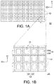
- FIG. 1A is a top view of a touch display apparatus according to an embodiment of the invention.
- FIG. 1B is an enlarged view of a touch display unit of FIG. 1A .
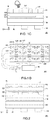
- FIG. 1C is a cross-sectional view of the touch display unit of FIG. 1B .
- FIG. 1D is a schematic diagram of a bottom view of the touch display apparatus of FIG. 1A .
- the touch display apparatus of the embodiment has a first surface.
- the touch display apparatus 300 includes at least one touch display unit 100, and each of the touch display units 100 has the first surface.
- Each of the touch display units 100 includes a plurality of light-emitting elements 110, a first touch electrode layer 120 and a second touch electrode layer 130.
- the light-emitting element 110 is a light-emitting diode (LED)
- the touch display apparatus 300 is a LED display apparatus having a touch function.
- the plurality of light-emitting elements 110 are located on a first surface AA of a substrate.
- the substrate is, for example, made of a polyester material (PET), though the invention is not limited thereto.
- PET polyester material
- the substrate is disposed between the first touch electrode layer 120 and the second touch electrode layer 130.
- the first touch electrode layer 120 is also located on the first surface AA.
- the light emitting element 110 and the first touch electrode layer 120 are located on a same plane.
- the first touch electrode layer 120 of the touch display unit 100 has a plurality of first axial electrodes 120X extending along a first direction D1.
- the second touch electrode layer 130 has a plurality of second axial electrodes 130Y extending along a second direction D2.
- the first direction D1 is substantially perpendicular to the second direction D2, though the invention is not limited thereto.
- the second axial electrodes 130Y and the first axial electrodes 120X are disposed on two opposite surfaces of the substrate.
- the first touch electrode layer 120 is located between a touch object (for example, a hand) and the second touch electrode layer 130.
- orthographic projections of the first axial electrodes 120X on the first surface AA and orthographic projections of the second axial electrodes 130Y on the first surface AA commonly surround a plurality of closed regions CR, and the plurality of light-emitting elements 110 are respectively located in the corresponding closed region CR.
- one closed region CR is configured with one light-emitting element 110, though the invention is not limited thereto, and in other embodiments, as the size of the light-emitting element 110 becomes smaller, the number of the light-emitting elements 110 configured in the single closed region CR may be plural.
- the touch display apparatus 300 may sense and calculate a touch position of the touch object according to the capacitance variations, so as to achieve good reliability.
- the touch display apparatus 300 adopts the first touch electrode layer 120 and the second touch electrode layer 130 to achieve the touch function, it is unnecessary to set high-cost sensors, and the touch display apparatus 300 may achieve a multi-touch function.
- the touch display unit 100 has a bottom surface BS, and the first surface AA is opposite to the bottom surface BS, and each of the touch display units 100 further includes a plurality of driving units 140.
- the driving units 140 are, for example, LED driving circuits.
- each of the touch display units 100 may include a single driving unit 140.
- the driving units 140 are located on the bottom surface BS, where the light-emitting elements 110 are electrically connected to the driving units 140. In this way, the light-emitting elements 110 may be respectively controlled by the driving units 140 disposed on the bottom surface BS to light up, so that the touch display apparatus 300 achieves a function of display images.
- the touch display apparatus 300 further includes a grounding layer 150 and a Printed Circuit Board (PCB) 160 located between the driving units 140 and the second touch electrode layer 130.
- the PCB 160 may be configured with a plurality of traces (electrical connection lines) (not shown) used for electrically connecting the driving units 140, the light-emitting elements 110 or other components required to be electrically connected.
- the PCB 160 for example, presents a black color, e.g. has a black color or a covering in black on the surface facing the light-emitting elements 110, so as to improve contrast of a display image viewed by the user.
- the grounding layer 150 is located between the PCB 160 and the second touch electrode layer 130.
- the touch display apparatus 300 may isolate interference on the second touch electrode layer 130 or the first touch electrode layer 120 caused by noises generated from the traces on the PCB 160 through configuration of the grounding layer 150, so as to achieve a good touch function.
- the touch display apparatus 300 further includes a hardened layer 170 covering the light-emitting elements 110.
- the hardened layer 170 may be a hardened Optically Clear Adhesives (OCA) layer, which is adapted to light penetration.
- OCA Optically Clear Adhesives
- a surface of the hardened layer 170 away from the first surface AA is, for example, a polished surface, which improves comfort of the touch.
- the surface of the hardened layer 170 away from the first surface AA is, for example, a rough surface, which improves a user experience of the touch.
- the touch display apparatus 300 further includes a plurality of first leads CL and a control unit 180, which are all located on the bottom surface BS.
- the control unit 180 is, for example, a touch signal processor, which is used for determining a coordinate position of the touch point, or other programmable general purpose or special purpose microprocessor, a Digital Signal Processor (DSP), a programmable controller, an Application Specific Integrated Circuits (ASIC), a Programmable Logic Device (PLD), or other similar device or a combination of the above devices.
- DSP Digital Signal Processor
- ASIC Application Specific Integrated Circuits
- PLD Programmable Logic Device
- FIG. ID is a schematic diagram of a bottom view of the touch display unit of FIG. 1A .
- each of the touch display units 100 further includes a first touch electrode layer connection terminal 120A and a second touch electrode layer connection terminal 130A.
- the first touch electrode layer connection terminal 120A is electrically connected to the first touch electrode layer 120 through internal leads (not shown) penetrating through the PCB 160.
- the second touch electrode layer connection terminal 130A is electrically connected to the second touch electrode layer 130 through the internal leads (not shown) penetrating through the PCB 160.
- the first leads CL respectively have first ends and second ends.
- the first ends of the first leads CL are respectively electrically connected to the first touch electrode layer connection terminal 120A and the second touch electrode layer 130 of each of the touch display units 100. It should be noted that the first ends of the first leads CL connect a plurality of touch display units 100 at the outermost periphery of the touch display apparatus 300, where at least one side of each of the touch display units 100 at the outermost periphery does not contact another touch display unit 100.
- the second ends of the first leads CL are electrically connected to the control unit 180.
- the second leads CL' are used for electrically connecting a plurality of first touch electrode layer connection terminals 120A of a plurality of adjacent touch display units 100, and the second leads CL' are used for electrically connecting a plurality of second touch electrode layer connection terminals 130A of a plurality of adjacent touch display units 100.
- the control unit 180 is also electrically connected to the first touch electrode layer connection terminals 120A and the second touch electrode layer connection terminals 130A of the touch display units 100 through the first leads CL.
- the touch display units 100 may be electrically connected through the second leads CL'. Moreover, through the electrical connection of the first touch electrode layer connection terminals 120A and the second touch electrode layer connection terminals 130A, the first touch electrode layer 120 and the second touch electrode layer 130 may be respectively electrically connected to the first touch electrode layer 120 and the second touch electrode layer 130 of the other touch display unit 100, so as to expand a touch range, and implement the touch detection function of each of the touch display units 100.
- first leads CL and the second leads CL' are disposed on the bottom surface BS without passing through the first surface AA, it is unnecessary to additionally set a border to shield the first leads CL, so as to achieve a borderless design, and the touch display units 100 may be designed and arranged according to an actual requirement, and may be arbitrarily expanded to form different contours of the touch display apparatus 300.
- the touch display apparatus 300 may sense and calculate a touch position according to the capacitance variations of the axial electrodes therein, so as to implement the touch function. Moreover, since the touch display apparatus 300 implements the display and touch functions simultaneously by integrates the LED display apparatus and the capacitive touch technique based on the configuration that the light emitting elements 110 and the first touch electrode layer 120 are all located on the first surface AA, the touch display apparatus 300 is not affected by environmental light and dust, and is not easy to cause misjudgement, so as to achieve good reliability.
- the touch display apparatus 300 may also achieve the borderless design through the configuration of the first leads CL on the bottom surface BS, and the touch display units 100 may be designed and arranged according to an actual requirement, and may be arbitrarily expanded to form different contours of the touch display apparatus 300.
- FIG. 2 is a cross-sectional view of another touch display unit according to an embodiment of the invention.
- the touch display unit 200 of FIG. 2 is similar to the touch display unit 100 of FIG. 1C , and differences there between are as follows.
- the first touch electrode layer 120 and the light emitting elements 110 are not located on a same plane.
- the touch display unit 200 further includes an optical film 210 and a cover 220, where the cover 220 is located on the optical film 210.
- the optical film 210 and the cover 220 are, for example, made of a transparent material.
- the optical film 210 has a first side S1 and a second side S2 opposite to each other, and the first touch electrode layer 120 and the second touch electrode layer 130 of each touch display unit 200 are respectively located on the first side S1 and the second side S2 of the optical film 210.
- the material of the optical film 210 may be a polyester film (PET film), though the invention is not limited thereto.
- the optical film 210 may also be replaced by glass.
- the optical film 210 covers the light-emitting elements 110.
- the method of covering the light-emitting elements 110 by the optical film 210 in the touch display unit 200 is implemented by respectively forming the first touch electrode layer 120 and the second touch electrode layer 130 on the first side S1 and the second side S2 of the optical film 210, and then adhering the optical film 210 on the light-emitting elements 110.
- the second touch electrode layer 130 is located between the light-emitting elements 110 and the first touch electrode layer 120.
- the touch display unit 200 may also sense and calculate a touch position according to the capacitance variations of the axial electrodes therein based on the configuration of the first touch electrode layer 120 and the second touch electrode layer 130, so as to implement the touch function, and the touch display unit 200 is adapted to be applied to the aforementioned touch display apparatus 300. Moreover, when the touch display unit 200 is applied to the aforementioned touch display apparatus 300, the touch display apparatus 300 may also achieve the aforementioned effects and advantages, and details thereof are not repeated.
- a plurality of PCBs 160 and the light-emitting elements 110 thereon are arranged into a required size and contour in an array, and then the optical film 210 and the first touch electrode layer 120 and the second touch electrode layer 130 thereon are adhered on the light-emitting elements 110.
- the embodiment of the invention has at least one of following advantages or effects.
- the touch display apparatus sense and calculate a touch position according to a capacitance variation of the axial electrodes therein, so as to implement the touch function.
- the touch display apparatus implements the display function and the touch function simultaneously by integrates a display device and a capacitive touch technique based on the configuration that the light-emitting elements and the first touch electrode layer are all located on the first surface, it is not affected by environmental light and dust, and is not easy to cause misjudgement, and has good reliability.
- the touch display apparatus may also achieve a borderless effect based on the configuration of the leads on the bottom surface, and the touch display units may be designed and arranged according to an actual requirement, and may be arbitrarily expanded to form different contours of the touch display apparatus.
- the term "the invention”, “the present invention” or the like does not necessarily limit the claim scope to a specific embodiment, and the reference to particularly preferred exemplary embodiments of the invention does not imply a limitation on the invention, and no such limitation is to be inferred.
- the invention is limited only by the scope of the appended claims.
- the abstract of the disclosure is provided to comply with the rules requiring an abstract, which will allow a searcher to quickly ascertain the subject matter of the technical disclosure of any patent issued from this disclosure. It is submitted with the understanding that it will not be used to interpret or limit the scope or meaning of the claims. Any advantages and benefits described may not apply to all embodiments of the invention.
Landscapes
- Engineering & Computer Science (AREA)
- General Engineering & Computer Science (AREA)
- Theoretical Computer Science (AREA)
- Human Computer Interaction (AREA)
- Physics & Mathematics (AREA)
- General Physics & Mathematics (AREA)
- Computer Networks & Wireless Communication (AREA)
- Devices For Indicating Variable Information By Combining Individual Elements (AREA)
Applications Claiming Priority (1)
| Application Number | Priority Date | Filing Date | Title |
|---|---|---|---|
| CN201811283710.4A CN111124167A (zh) | 2018-10-31 | 2018-10-31 | 触控显示装置 |
Publications (1)
| Publication Number | Publication Date |
|---|---|
| EP3647920A1 true EP3647920A1 (fr) | 2020-05-06 |
Family
ID=68382307
Family Applications (1)
| Application Number | Title | Priority Date | Filing Date |
|---|---|---|---|
| EP19205639.8A Withdrawn EP3647920A1 (fr) | 2018-10-31 | 2019-10-28 | Appareil d'affichage tactile |
Country Status (3)
| Country | Link |
|---|---|
| US (1) | US20200133437A1 (fr) |
| EP (1) | EP3647920A1 (fr) |
| CN (1) | CN111124167A (fr) |
Families Citing this family (4)
| Publication number | Priority date | Publication date | Assignee | Title |
|---|---|---|---|---|
| CN112506373A (zh) | 2020-11-30 | 2021-03-16 | 合肥鑫晟光电科技有限公司 | 触控基板及其制备方法、显示装置 |
| CN116416875A (zh) * | 2021-12-28 | 2023-07-11 | 西安青松光电技术有限公司 | Led显示单元及显示屏 |
| CN114582918B (zh) * | 2022-03-04 | 2026-03-17 | Tcl华星光电技术有限公司 | 显示面板 |
| CN119781636A (zh) * | 2023-10-07 | 2025-04-08 | Tcl华星光电技术有限公司 | 显示面板和电子设备 |
Citations (2)
| Publication number | Priority date | Publication date | Assignee | Title |
|---|---|---|---|---|
| US20130135229A1 (en) * | 2011-11-25 | 2013-05-30 | Henghao Technology Co. Ltd | Touch panel and touch display panel using the same |
| US20140139761A1 (en) * | 2011-07-25 | 2014-05-22 | Panasonic Corporation | Display device |
Family Cites Families (2)
| Publication number | Priority date | Publication date | Assignee | Title |
|---|---|---|---|---|
| JP2014219816A (ja) * | 2013-05-08 | 2014-11-20 | 株式会社ジャパンディスプレイ | タッチパネル付き表示装置 |
| CN108089760B (zh) * | 2018-01-02 | 2022-03-04 | 武汉天马微电子有限公司 | 一种触控显示面板及触控显示装置 |
-
2018
- 2018-10-31 CN CN201811283710.4A patent/CN111124167A/zh active Pending
-
2019
- 2019-10-28 EP EP19205639.8A patent/EP3647920A1/fr not_active Withdrawn
- 2019-10-29 US US16/667,839 patent/US20200133437A1/en not_active Abandoned
Patent Citations (2)
| Publication number | Priority date | Publication date | Assignee | Title |
|---|---|---|---|---|
| US20140139761A1 (en) * | 2011-07-25 | 2014-05-22 | Panasonic Corporation | Display device |
| US20130135229A1 (en) * | 2011-11-25 | 2013-05-30 | Henghao Technology Co. Ltd | Touch panel and touch display panel using the same |
Also Published As
| Publication number | Publication date |
|---|---|
| US20200133437A1 (en) | 2020-04-30 |
| CN111124167A (zh) | 2020-05-08 |
Similar Documents
| Publication | Publication Date | Title |
|---|---|---|
| US12086370B2 (en) | Touch input device | |
| US11182000B2 (en) | Smartphone | |
| CN102096526B (zh) | 光学传感单元、显示模块和使用光学传感单元的显示装置 | |
| US8366286B2 (en) | Light-transmissive input device and method of manufacturing the same | |
| CN102109933B (zh) | 具有显示面板和光学传感框架的组件及使用其的显示系统 | |
| EP3647920A1 (fr) | Appareil d'affichage tactile | |
| KR102175563B1 (ko) | 터치 패널 | |
| EP2339438B1 (fr) | Système d'entrée tactile optique et procédé d'établissement de référence dans celui-ci | |
| US8976156B2 (en) | Camera module and optical touch screen using the same | |
| US20170177107A1 (en) | Infrared Touch Screen, Touch Detection Method and Display Apparatus | |
| CN108121479A (zh) | 显示装置 | |
| KR20190010244A (ko) | 터치 방식 표시장치 및 터치 감지방법 | |
| JP6318023B2 (ja) | 表示装置の駆動方法 | |
| CN104461155A (zh) | 一种内嵌式触控显示屏及显示装置 | |
| CN105022533A (zh) | 显示模块 | |
| JP2005190950A (ja) | 入力装置 | |
| KR101655427B1 (ko) | 3차원 터치 스크린 패널 | |
| KR101351420B1 (ko) | 광학 센싱 프레임을 갖는 표시 장치 | |
| KR101655429B1 (ko) | 3차원 터치 스크린 패널 | |
| KR100868824B1 (ko) | 광학방식 터치스크린 | |
| KR101760513B1 (ko) | 광학 터치 스크린의 조립 방법 | |
| JP2024124816A (ja) | 検出装置 | |
| KR101655431B1 (ko) | 3차원 터치 스크린 패널 | |
| KR20170072066A (ko) | 터치표시장치 | |
| KR20060134627A (ko) | 디스플레이 패널의 전면필터 |
Legal Events
| Date | Code | Title | Description |
|---|---|---|---|
| PUAI | Public reference made under article 153(3) epc to a published international application that has entered the european phase |
Free format text: ORIGINAL CODE: 0009012 |
|
| STAA | Information on the status of an ep patent application or granted ep patent |
Free format text: STATUS: THE APPLICATION HAS BEEN PUBLISHED |
|
| AK | Designated contracting states |
Kind code of ref document: A1 Designated state(s): AL AT BE BG CH CY CZ DE DK EE ES FI FR GB GR HR HU IE IS IT LI LT LU LV MC MK MT NL NO PL PT RO RS SE SI SK SM TR |
|
| AX | Request for extension of the european patent |
Extension state: BA ME |
|
| STAA | Information on the status of an ep patent application or granted ep patent |
Free format text: STATUS: REQUEST FOR EXAMINATION WAS MADE |
|
| 17P | Request for examination filed |
Effective date: 20201028 |
|
| RBV | Designated contracting states (corrected) |
Designated state(s): AL AT BE BG CH CY CZ DE DK EE ES FI FR GB GR HR HU IE IS IT LI LT LU LV MC MK MT NL NO PL PT RO RS SE SI SK SM TR |
|
| STAA | Information on the status of an ep patent application or granted ep patent |
Free format text: STATUS: THE APPLICATION HAS BEEN WITHDRAWN |
|
| 18W | Application withdrawn |
Effective date: 20210709 |