EP3648085A1 - Elektronische vorrichtung - Google Patents
Elektronische vorrichtung Download PDFInfo
- Publication number
- EP3648085A1 EP3648085A1 EP18825219.1A EP18825219A EP3648085A1 EP 3648085 A1 EP3648085 A1 EP 3648085A1 EP 18825219 A EP18825219 A EP 18825219A EP 3648085 A1 EP3648085 A1 EP 3648085A1
- Authority
- EP
- European Patent Office
- Prior art keywords
- display
- display panel
- light
- substrate
- electronic device
- Prior art date
- Legal status (The legal status is an assumption and is not a legal conclusion. Google has not performed a legal analysis and makes no representation as to the accuracy of the status listed.)
- Ceased
Links
Images






Classifications
-
- G—PHYSICS
- G09—EDUCATION; CRYPTOGRAPHY; DISPLAY; ADVERTISING; SEALS
- G09G—ARRANGEMENTS OR CIRCUITS FOR CONTROL OF INDICATING DEVICES USING STATIC MEANS TO PRESENT VARIABLE INFORMATION
- G09G3/00—Control arrangements or circuits, of interest only in connection with visual indicators other than cathode-ray tubes
- G09G3/20—Control arrangements or circuits, of interest only in connection with visual indicators other than cathode-ray tubes for presentation of an assembly of a number of characters, e.g. a page, by composing the assembly by combination of individual elements arranged in a matrix no fixed position being assigned to or needed to be assigned to the individual characters or partial characters
-
- G—PHYSICS
- G02—OPTICS
- G02F—OPTICAL DEVICES OR ARRANGEMENTS FOR THE CONTROL OF LIGHT BY MODIFICATION OF THE OPTICAL PROPERTIES OF THE MEDIA OF THE ELEMENTS INVOLVED THEREIN; NON-LINEAR OPTICS; FREQUENCY-CHANGING OF LIGHT; OPTICAL LOGIC ELEMENTS; OPTICAL ANALOGUE/DIGITAL CONVERTERS
- G02F1/00—Devices or arrangements for the control of the intensity, colour, phase, polarisation or direction of light arriving from an independent light source, e.g. switching, gating or modulating; Non-linear optics
- G02F1/01—Devices or arrangements for the control of the intensity, colour, phase, polarisation or direction of light arriving from an independent light source, e.g. switching, gating or modulating; Non-linear optics for the control of the intensity, phase, polarisation or colour
- G02F1/13—Devices or arrangements for the control of the intensity, colour, phase, polarisation or direction of light arriving from an independent light source, e.g. switching, gating or modulating; Non-linear optics for the control of the intensity, phase, polarisation or colour based on liquid crystals, e.g. single liquid crystal display cells
- G02F1/133—Constructional arrangements; Operation of liquid crystal cells; Circuit arrangements
- G02F1/1333—Constructional arrangements; Manufacturing methods
- G02F1/13338—Input devices, e.g. touch panels
-
- G—PHYSICS
- G02—OPTICS
- G02F—OPTICAL DEVICES OR ARRANGEMENTS FOR THE CONTROL OF LIGHT BY MODIFICATION OF THE OPTICAL PROPERTIES OF THE MEDIA OF THE ELEMENTS INVOLVED THEREIN; NON-LINEAR OPTICS; FREQUENCY-CHANGING OF LIGHT; OPTICAL LOGIC ELEMENTS; OPTICAL ANALOGUE/DIGITAL CONVERTERS
- G02F1/00—Devices or arrangements for the control of the intensity, colour, phase, polarisation or direction of light arriving from an independent light source, e.g. switching, gating or modulating; Non-linear optics
- G02F1/01—Devices or arrangements for the control of the intensity, colour, phase, polarisation or direction of light arriving from an independent light source, e.g. switching, gating or modulating; Non-linear optics for the control of the intensity, phase, polarisation or colour
- G02F1/13—Devices or arrangements for the control of the intensity, colour, phase, polarisation or direction of light arriving from an independent light source, e.g. switching, gating or modulating; Non-linear optics for the control of the intensity, phase, polarisation or colour based on liquid crystals, e.g. single liquid crystal display cells
- G02F1/133—Constructional arrangements; Operation of liquid crystal cells; Circuit arrangements
- G02F1/1333—Constructional arrangements; Manufacturing methods
- G02F1/1334—Constructional arrangements; Manufacturing methods based on polymer dispersed liquid crystals, e.g. microencapsulated liquid crystals
-
- G—PHYSICS
- G02—OPTICS
- G02F—OPTICAL DEVICES OR ARRANGEMENTS FOR THE CONTROL OF LIGHT BY MODIFICATION OF THE OPTICAL PROPERTIES OF THE MEDIA OF THE ELEMENTS INVOLVED THEREIN; NON-LINEAR OPTICS; FREQUENCY-CHANGING OF LIGHT; OPTICAL LOGIC ELEMENTS; OPTICAL ANALOGUE/DIGITAL CONVERTERS
- G02F1/00—Devices or arrangements for the control of the intensity, colour, phase, polarisation or direction of light arriving from an independent light source, e.g. switching, gating or modulating; Non-linear optics
- G02F1/01—Devices or arrangements for the control of the intensity, colour, phase, polarisation or direction of light arriving from an independent light source, e.g. switching, gating or modulating; Non-linear optics for the control of the intensity, phase, polarisation or colour
- G02F1/13—Devices or arrangements for the control of the intensity, colour, phase, polarisation or direction of light arriving from an independent light source, e.g. switching, gating or modulating; Non-linear optics for the control of the intensity, phase, polarisation or colour based on liquid crystals, e.g. single liquid crystal display cells
- G02F1/133—Constructional arrangements; Operation of liquid crystal cells; Circuit arrangements
- G02F1/1333—Constructional arrangements; Manufacturing methods
- G02F1/1335—Structural association of cells with optical devices, e.g. polarisers or reflectors
- G02F1/1336—Illuminating devices
- G02F1/133602—Direct backlight
- G02F1/133603—Direct backlight with LEDs
-
- G—PHYSICS
- G02—OPTICS
- G02F—OPTICAL DEVICES OR ARRANGEMENTS FOR THE CONTROL OF LIGHT BY MODIFICATION OF THE OPTICAL PROPERTIES OF THE MEDIA OF THE ELEMENTS INVOLVED THEREIN; NON-LINEAR OPTICS; FREQUENCY-CHANGING OF LIGHT; OPTICAL LOGIC ELEMENTS; OPTICAL ANALOGUE/DIGITAL CONVERTERS
- G02F1/00—Devices or arrangements for the control of the intensity, colour, phase, polarisation or direction of light arriving from an independent light source, e.g. switching, gating or modulating; Non-linear optics
- G02F1/01—Devices or arrangements for the control of the intensity, colour, phase, polarisation or direction of light arriving from an independent light source, e.g. switching, gating or modulating; Non-linear optics for the control of the intensity, phase, polarisation or colour
- G02F1/13—Devices or arrangements for the control of the intensity, colour, phase, polarisation or direction of light arriving from an independent light source, e.g. switching, gating or modulating; Non-linear optics for the control of the intensity, phase, polarisation or colour based on liquid crystals, e.g. single liquid crystal display cells
- G02F1/133—Constructional arrangements; Operation of liquid crystal cells; Circuit arrangements
- G02F1/1333—Constructional arrangements; Manufacturing methods
- G02F1/1335—Structural association of cells with optical devices, e.g. polarisers or reflectors
- G02F1/1336—Illuminating devices
- G02F1/133621—Illuminating devices providing coloured light
-
- G—PHYSICS
- G02—OPTICS
- G02F—OPTICAL DEVICES OR ARRANGEMENTS FOR THE CONTROL OF LIGHT BY MODIFICATION OF THE OPTICAL PROPERTIES OF THE MEDIA OF THE ELEMENTS INVOLVED THEREIN; NON-LINEAR OPTICS; FREQUENCY-CHANGING OF LIGHT; OPTICAL LOGIC ELEMENTS; OPTICAL ANALOGUE/DIGITAL CONVERTERS
- G02F1/00—Devices or arrangements for the control of the intensity, colour, phase, polarisation or direction of light arriving from an independent light source, e.g. switching, gating or modulating; Non-linear optics
- G02F1/01—Devices or arrangements for the control of the intensity, colour, phase, polarisation or direction of light arriving from an independent light source, e.g. switching, gating or modulating; Non-linear optics for the control of the intensity, phase, polarisation or colour
- G02F1/13—Devices or arrangements for the control of the intensity, colour, phase, polarisation or direction of light arriving from an independent light source, e.g. switching, gating or modulating; Non-linear optics for the control of the intensity, phase, polarisation or colour based on liquid crystals, e.g. single liquid crystal display cells
- G02F1/133—Constructional arrangements; Operation of liquid crystal cells; Circuit arrangements
- G02F1/1333—Constructional arrangements; Manufacturing methods
- G02F1/1343—Electrodes
- G02F1/134309—Electrodes characterised by their geometrical arrangement
- G02F1/134327—Segmented, e.g. alpha numeric display
-
- G—PHYSICS
- G02—OPTICS
- G02F—OPTICAL DEVICES OR ARRANGEMENTS FOR THE CONTROL OF LIGHT BY MODIFICATION OF THE OPTICAL PROPERTIES OF THE MEDIA OF THE ELEMENTS INVOLVED THEREIN; NON-LINEAR OPTICS; FREQUENCY-CHANGING OF LIGHT; OPTICAL LOGIC ELEMENTS; OPTICAL ANALOGUE/DIGITAL CONVERTERS
- G02F1/00—Devices or arrangements for the control of the intensity, colour, phase, polarisation or direction of light arriving from an independent light source, e.g. switching, gating or modulating; Non-linear optics
- G02F1/01—Devices or arrangements for the control of the intensity, colour, phase, polarisation or direction of light arriving from an independent light source, e.g. switching, gating or modulating; Non-linear optics for the control of the intensity, phase, polarisation or colour
- G02F1/13—Devices or arrangements for the control of the intensity, colour, phase, polarisation or direction of light arriving from an independent light source, e.g. switching, gating or modulating; Non-linear optics for the control of the intensity, phase, polarisation or colour based on liquid crystals, e.g. single liquid crystal display cells
- G02F1/133—Constructional arrangements; Operation of liquid crystal cells; Circuit arrangements
- G02F1/1333—Constructional arrangements; Manufacturing methods
- G02F1/1347—Arrangement of liquid crystal layers or cells in which the final condition of one light beam is achieved by the addition of the effects of two or more layers or cells
- G02F1/13476—Arrangement of liquid crystal layers or cells in which the final condition of one light beam is achieved by the addition of the effects of two or more layers or cells in which at least one liquid crystal cell or layer assumes a scattering state
-
- G—PHYSICS
- G04—HOROLOGY
- G04G—ELECTRONIC TIME-PIECES
- G04G17/00—Structural details; Housings
- G04G17/02—Component assemblies
- G04G17/04—Mounting of electronic components
- G04G17/045—Mounting of the display
-
- G—PHYSICS
- G06—COMPUTING OR CALCULATING; COUNTING
- G06F—ELECTRIC DIGITAL DATA PROCESSING
- G06F1/00—Details not covered by groups G06F3/00 - G06F13/00 and G06F21/00
- G06F1/16—Constructional details or arrangements
- G06F1/1613—Constructional details or arrangements for portable computers
- G06F1/163—Wearable computers, e.g. on a belt
-
- G—PHYSICS
- G06—COMPUTING OR CALCULATING; COUNTING
- G06F—ELECTRIC DIGITAL DATA PROCESSING
- G06F3/00—Input arrangements for transferring data to be processed into a form capable of being handled by the computer; Output arrangements for transferring data from processing unit to output unit, e.g. interface arrangements
- G06F3/14—Digital output to display device ; Cooperation and interconnection of the display device with other functional units
- G06F3/1423—Digital output to display device ; Cooperation and interconnection of the display device with other functional units controlling a plurality of local displays, e.g. CRT and flat panel display
-
- G—PHYSICS
- G09—EDUCATION; CRYPTOGRAPHY; DISPLAY; ADVERTISING; SEALS
- G09F—DISPLAYING; ADVERTISING; SIGNS; LABELS OR NAME-PLATES; SEALS
- G09F9/00—Indicating arrangements for variable information in which the information is built-up on a support by selection or combination of individual elements
- G09F9/30—Indicating arrangements for variable information in which the information is built-up on a support by selection or combination of individual elements in which the desired character or characters are formed by combining individual elements
- G09F9/35—Indicating arrangements for variable information in which the information is built-up on a support by selection or combination of individual elements in which the desired character or characters are formed by combining individual elements being liquid crystals
-
- G—PHYSICS
- G09—EDUCATION; CRYPTOGRAPHY; DISPLAY; ADVERTISING; SEALS
- G09F—DISPLAYING; ADVERTISING; SIGNS; LABELS OR NAME-PLATES; SEALS
- G09F9/00—Indicating arrangements for variable information in which the information is built-up on a support by selection or combination of individual elements
- G09F9/46—Indicating arrangements for variable information in which the information is built-up on a support by selection or combination of individual elements in which the desired character is selected from a number of characters arranged one behind the other
-
- H—ELECTRICITY
- H10—SEMICONDUCTOR DEVICES; ELECTRIC SOLID-STATE DEVICES NOT OTHERWISE PROVIDED FOR
- H10K—ORGANIC ELECTRIC SOLID-STATE DEVICES
- H10K59/00—Integrated devices, or assemblies of multiple devices, comprising at least one organic light-emitting element covered by group H10K50/00
- H10K59/30—Devices specially adapted for multicolour light emission
- H10K59/35—Devices specially adapted for multicolour light emission comprising red-green-blue [RGB] subpixels
-
- G—PHYSICS
- G02—OPTICS
- G02F—OPTICAL DEVICES OR ARRANGEMENTS FOR THE CONTROL OF LIGHT BY MODIFICATION OF THE OPTICAL PROPERTIES OF THE MEDIA OF THE ELEMENTS INVOLVED THEREIN; NON-LINEAR OPTICS; FREQUENCY-CHANGING OF LIGHT; OPTICAL LOGIC ELEMENTS; OPTICAL ANALOGUE/DIGITAL CONVERTERS
- G02F1/00—Devices or arrangements for the control of the intensity, colour, phase, polarisation or direction of light arriving from an independent light source, e.g. switching, gating or modulating; Non-linear optics
- G02F1/01—Devices or arrangements for the control of the intensity, colour, phase, polarisation or direction of light arriving from an independent light source, e.g. switching, gating or modulating; Non-linear optics for the control of the intensity, phase, polarisation or colour
- G02F1/13—Devices or arrangements for the control of the intensity, colour, phase, polarisation or direction of light arriving from an independent light source, e.g. switching, gating or modulating; Non-linear optics for the control of the intensity, phase, polarisation or colour based on liquid crystals, e.g. single liquid crystal display cells
- G02F1/133—Constructional arrangements; Operation of liquid crystal cells; Circuit arrangements
- G02F1/1333—Constructional arrangements; Manufacturing methods
- G02F1/1334—Constructional arrangements; Manufacturing methods based on polymer dispersed liquid crystals, e.g. microencapsulated liquid crystals
- G02F1/13345—Network or three-dimensional gels
-
- G—PHYSICS
- G02—OPTICS
- G02F—OPTICAL DEVICES OR ARRANGEMENTS FOR THE CONTROL OF LIGHT BY MODIFICATION OF THE OPTICAL PROPERTIES OF THE MEDIA OF THE ELEMENTS INVOLVED THEREIN; NON-LINEAR OPTICS; FREQUENCY-CHANGING OF LIGHT; OPTICAL LOGIC ELEMENTS; OPTICAL ANALOGUE/DIGITAL CONVERTERS
- G02F1/00—Devices or arrangements for the control of the intensity, colour, phase, polarisation or direction of light arriving from an independent light source, e.g. switching, gating or modulating; Non-linear optics
- G02F1/01—Devices or arrangements for the control of the intensity, colour, phase, polarisation or direction of light arriving from an independent light source, e.g. switching, gating or modulating; Non-linear optics for the control of the intensity, phase, polarisation or colour
- G02F1/13—Devices or arrangements for the control of the intensity, colour, phase, polarisation or direction of light arriving from an independent light source, e.g. switching, gating or modulating; Non-linear optics for the control of the intensity, phase, polarisation or colour based on liquid crystals, e.g. single liquid crystal display cells
- G02F1/133—Constructional arrangements; Operation of liquid crystal cells; Circuit arrangements
- G02F1/1333—Constructional arrangements; Manufacturing methods
- G02F1/1335—Structural association of cells with optical devices, e.g. polarisers or reflectors
- G02F1/1336—Illuminating devices
- G02F1/133626—Illuminating devices providing two modes of illumination, e.g. day-night
-
- G—PHYSICS
- G02—OPTICS
- G02F—OPTICAL DEVICES OR ARRANGEMENTS FOR THE CONTROL OF LIGHT BY MODIFICATION OF THE OPTICAL PROPERTIES OF THE MEDIA OF THE ELEMENTS INVOLVED THEREIN; NON-LINEAR OPTICS; FREQUENCY-CHANGING OF LIGHT; OPTICAL LOGIC ELEMENTS; OPTICAL ANALOGUE/DIGITAL CONVERTERS
- G02F2201/00—Constructional arrangements not provided for in groups G02F1/00 - G02F7/00
- G02F2201/05—Constructional arrangements not provided for in groups G02F1/00 - G02F7/00 multimode
-
- G—PHYSICS
- G02—OPTICS
- G02F—OPTICAL DEVICES OR ARRANGEMENTS FOR THE CONTROL OF LIGHT BY MODIFICATION OF THE OPTICAL PROPERTIES OF THE MEDIA OF THE ELEMENTS INVOLVED THEREIN; NON-LINEAR OPTICS; FREQUENCY-CHANGING OF LIGHT; OPTICAL LOGIC ELEMENTS; OPTICAL ANALOGUE/DIGITAL CONVERTERS
- G02F2201/00—Constructional arrangements not provided for in groups G02F1/00 - G02F7/00
- G02F2201/44—Arrangements combining different electro-active layers, e.g. electrochromic, liquid crystal or electroluminescent layers
-
- G—PHYSICS
- G02—OPTICS
- G02F—OPTICAL DEVICES OR ARRANGEMENTS FOR THE CONTROL OF LIGHT BY MODIFICATION OF THE OPTICAL PROPERTIES OF THE MEDIA OF THE ELEMENTS INVOLVED THEREIN; NON-LINEAR OPTICS; FREQUENCY-CHANGING OF LIGHT; OPTICAL LOGIC ELEMENTS; OPTICAL ANALOGUE/DIGITAL CONVERTERS
- G02F2203/00—Function characteristic
- G02F2203/02—Function characteristic reflective
-
- G—PHYSICS
- G09—EDUCATION; CRYPTOGRAPHY; DISPLAY; ADVERTISING; SEALS
- G09G—ARRANGEMENTS OR CIRCUITS FOR CONTROL OF INDICATING DEVICES USING STATIC MEANS TO PRESENT VARIABLE INFORMATION
- G09G2300/00—Aspects of the constitution of display devices
- G09G2300/02—Composition of display devices
- G09G2300/023—Display panel composed of stacked panels
-
- H—ELECTRICITY
- H10—SEMICONDUCTOR DEVICES; ELECTRIC SOLID-STATE DEVICES NOT OTHERWISE PROVIDED FOR
- H10K—ORGANIC ELECTRIC SOLID-STATE DEVICES
- H10K59/00—Integrated devices, or assemblies of multiple devices, comprising at least one organic light-emitting element covered by group H10K50/00
- H10K59/10—OLED displays
- H10K59/12—Active-matrix OLED [AMOLED] displays
Definitions
- the present invention relates to an electronic device including a display device.
- organic EL display device using an organic electroluminescence element (organic EL element).
- organic EL element organic electroluminescence element
- the organic EL display device is of a self-luminescence type, and has such characteristics as a high contrast, a wide viewing angle and a high response speed.
- one of two electrodes, which sandwich an organic light-emission layer is composed of a metallic electrode which reflects light, and the other electrode is composed of a transparent electrode.
- the present invention provides an electronic device which can realize a plurality of display modes, while improving brightness.
- an electronic device comprising: a first display panel; a second display panel; a spacer configured to keep a distance between the first display panel and the second display panel; and an air layer which is provided between the first display panel and the second display panel and is surrounded by the spacer.
- the first display panel includes: first and second substrates; a plurality of pixel electrodes which are provided on the first substrate and reflect light; a plurality of light-emission layers which are provided on the pixel electrodes and emit light; and a first common electrode which is provided on the second substrate and is in contact with the light-emission layers.
- the second display panel includes: third and fourth substrates; a polymer dispersed liquid crystal layer filled between the third substrate and the fourth substrate; a plurality of display electrodes provided on the third substrate; and a second common electrode provided on the fourth substrate.
- the second substrate of the first display panel is disposed in such a manner as to directly face the second display panel.
- an electronic device which can realize a plurality of display modes, while improving brightness.
- an electronic watch will be described by way of example, as an electronic device including a display device.
- FIG. 1 is a block diagram of an electronic watch 1 according to a first embodiment of the present invention.
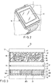
- FIG. 2 is a schematic view of the electronic watch 1.
- the electronic watch 1 includes a display unit 10, an EL driving circuit 13, a PN driving circuit 14, an oscillation circuit 15, a clock circuit 16, a storage unit 17, a power supply circuit 18, an input unit 19, and a control circuit 20.
- the display unit 10 includes a first display panel 11 and a second display panel 12.
- the first display panel (OEL) 11 is composed of an organic EL display element.
- the second display panel (PN-LCD) 11 is composed of a polymer dispersed liquid crystal display element. Concrete configurations of the first display panel 11 and second display panel 12 will be described later.
- the EL driving circuit 13 is electrically connected to a plurality of signal lines which are connected to the first display panel 11, and drives the first display panel 11.
- the PN driving circuit 14 is electrically connected to a plurality of signal lines which are connected to the second display panel 12, and drives the second display panel 12.
- the oscillation circuit 15 generates a clock signal having a fixed frequency.
- the clock circuit 16 calculates present time data and the like, by using the clock signal which is input from the oscillation circuit 15.
- the clock circuit 16 sends the calculated present time data, date data, etc., to the control circuit 20.
- the storage unit 17 includes, for example, a ROM (Read Only Memory) for data read, and a RAM (Random Access Memory) which is capable of data read and data write.
- the RAM is used as a working area of the control circuit 20.
- the storage unit 17 includes a program area which stores a system program, application programs, and the like for realizing various functions of the electronic watch 1, and a data area which stores various data such as image data.
- the power supply circuit 18 supplies various voltages to the respective modules in the electronic watch 1 via power supply lines.
- the power supply circuit 18 includes, for example, a button battery (primary battery).
- the input unit 19 includes a plurality of push buttons for instructing execution of various functions of the electronic watch 1. If the input unit 19 is operated by a user, time setting is performed, or various modes are selected, in response to the operation.
- the control circuit 20 controls the entire operation of the electronic watch 1.
- the control circuit 20 is composed of a CPU (Central Processing Unit), etc. For example, at a predetermined timing, or in response to a signal which is input from the input unit 19, the control circuit 20 reads out various programs stored in the ROM, loads the programs into the working area of the RAM, and executes instructions (controls) to the respective modules that constitute the electronic watch 1, or executes data transfer or the like, in accordance with the programs.
- a CPU Central Processing Unit
- the electronic watch 1 may include a camera function (imaging unit), a communication function, and the like.
- FIG. 3 is a cross-sectional view of the display unit 10.
- the display unit 10 includes the first display panel 11 and second display panel 12, and the first display panel 11 and second display panel 12 are stacked via a transparent member (e.g. air layer) 21.
- a transparent member e.g. air layer
- the first display panel 11 performs character display with a large information amount or image display (hereinafter referred to as "information display”), and can perform color display.
- the first display panel 11 is composed of an organic EL display element.
- the first display panel 11 is a self-luminescence-type display element, and can perform image display without using an illumination device (backlight).
- the second display panel 12 is of a pattern display type which performs character display with a small information amount and figure display (hereinafter referred to as "character display"), and can perform display of a transparent state and a scattered state, i.e. black-and-white display.
- the character display includes display of a character with a small information amount or a figure, and time display (segment display).
- the second display panel 12 is composed of, for example, a liquid crystal display panel selected from between a polymer dispersed liquid crystal (PDLC) and a polymer network liquid crystal (PNLC). Since the second display panel 12 does not use a polarizer, the amount of light absorbed in the second display panel 12 can greatly be reduced, and a bright screen can be obtained. In addition, the second display panel 12 can perform a display operation with low power consumption.
- the second display panel 12 performs the character display (including time display and standby display), and the first display panel 11 performs the information display with a greater information amount than the character display.
- the first display panel 11 and second display panel 12 are stacked via a transparent member 21.
- the transparent member 21 is in contact with a lower substrate 40 of the second display panel 12, and the refractive index of the transparent member 21 is set to be different from the refractive index of the lower substrate 40.
- the transparent member 21 may be a transparent material which meets the above-described condition, and may be a gas.
- the transparent member 21 is composed of, for example, an air layer 21.
- the first display panel 11 and second display panel 12 are attached by a spacer (or a seal member) 22.
- the spacer 22 has a function of holding the first display panel 11 and second display panel 12, with a distance being provided therebetween.
- the spacer 22 is formed in a rectangular shape, in such a manner as to surround an outer periphery of the second display panel 12 (and first display panel 11).
- the air layer 21 is provided between the first display panel 11 and second display panel 12, such that the air layer 21 is surrounded by the spacer 22.
- the air layer 21 between the first display panel 11 and second display panel 12 By providing the air layer 21 between the first display panel 11 and second display panel 12, incident light on the second display panel 12 from the display surface side is reflected by an interface between the lower substrate 40 and air layer 21. As a result, bright display by the second display panel 12 can be realized, and the contrast of the display unit 10 can be improved. Moreover, by using the air layer 21 as the transparent member 21, the cost of the display unit 10 can be reduced.
- the first display panel 11 adopts an active matrix driving method in which active elements are disposed in association with respective pixels.
- the first display panel 11 includes a TFT substrate 30 on which a TFT (Thin Film Transistor) functioning as an active element (switching element), a pixel electrode, etc. are formed; an opposite substrate 31 on which a common electrode is formed and which is disposed to be opposed to the TFT substrate 30; and a light-emission layer provided between the TFT substrate 30 and opposite substrate 31.
- the TFT substrate 30 and opposite substrate 31 are attached by a seal member 32.
- the light-emission layer is sealed between the TFT substrate 30 and opposite substrate 31 by the seal member 32.
- Each of the TFT substrate 30 and opposite substrate 31 is composed of a transparent substrate (e.g. a glass substrate or a plastic substrate).
- the TFT 33 includes a gate electrode which is electrically connected to a scanning line; a gate insulating film provided on the gate electrode; a semiconductor layer provided on the gate insulating film; and a source electrode and a drain electrode which are provided on the semiconductor layer and spaced apart from each other.
- the source electrode is electrically connected to a signal line.
- the pixel electrode 35 is electrically connected to the drain electrode of the TFT 33.
- the pixel electrode 35 is composed of a metal which can reflect light.
- the pixel electrode 35 reflects light, which is generated by the light-emission layer, toward the opposite substrate 31.
- An insulating layer 34 which is provided between the pixel electrode 35 and TFT substrate 30, is illustrated by depicting, in a simplified manner, an insulating material (including a gate insulating film) which is necessary for stacking the electrodes included in the TFT 33.
- a plurality of light-emission layers 36 are provided on a plurality of pixel electrodes 35, respectively.
- the light-emission layers 36 include a red light-emission layer 36R which emits red light, a green light-emission layer 36G which emits green light, and a blue light-emission layer 36B which emits blue light.
- a red light-emission layer 36R which emits red light
- a green light-emission layer 36G which emits green light
- a blue light-emission layer 36B which emits blue light.
- three light-emission layers 36R, 36G and 36B are illustrated by way of example. Actually, sets of light-emission layers 36R, 36G and 36B are arranged, for example, in a matrix.
- the red light-emission layer 36R, green light-emission layer 36G and blue light-emission layer 36B can be composed by using a well-known material.
- Each light-emission layer (organic layer) 36 may be composed of three layers, i.e. a hole transport layer, a light-emitting layer, and an electron transport layer.
- the hole transport layer has a function of transporting holes, which are injected from an interface with a lower electrode, to the light-emitting layer.
- the electron transport layer has a function of transporting electrons, which are injected from an interface with an upper electrode, to the light-emitting layer.
- the light-emitting layer has a function of emitting light by recombining the hole transported from the hole transport layer and the electron transported from the electron transport layer.
- the organic layer 36 may employ a 5-layer structure, or the like.
- the hole transport layer may be functionally divided into a hole injection layer and a hole transport layer in the order from the lower electrode side, and may be composed of these two layers.
- the electron transport layer may be functionally divided into an electron injection layer and an electron transport layer in the order from the upper electrode side, and may be composed of these two layers.
- a common electrode 37 is provided on the opposite substrate 31.
- the common electrode 37 is formed in a planar shape over the entire display area. In the example of FIG. 3 , the common electrode 37 is led out to the outside of the seal member 32.
- the common electrode 37 is composed of a transparent electrode, and ITO (indium-tin-oxide), for instance, is used.
- ITO indium-tin-oxide
- the common electrode 37 is in contact with the light-emission layers 36.
- the opposite substrate 31 and common electrode 37 seal the light-emission layer 36.
- the opposite substrate 31 is disposed in a manner to directly face the second display panel 12.
- the opposite substrate 31 is in contact with the air layer 21.
- the first display panel 11 may include an optical member for improving display characteristics, on that surface of the opposite substrate 31, which is opposite to the common electrode 37. In this case, this optical member is in contact with the air layer 21.
- the second display panel 12 includes the lower substrate 40 on which a display electrode is formed; an upper substrate 41 on which a common electrode is formed and which is disposed to be opposed to the lower substrate 40; and a liquid crystal layer 42 interposed between the lower substrate 40 and upper substrate 41. That surface of the upper substrate 41, which is opposite to the liquid crystal layer 42, is a display surface of the display unit 10.
- Each of the lower substrate 40 and upper substrate 41 is composed of a transparent substrate (e.g. a glass substrate or a plastic substrate).
- a plurality of display electrodes 43 are provided on the lower substrate 40.
- the display electrodes 43 are processed in a shape corresponding to a character which the second display panel 12 can display.
- a common electrode 44 is provided on the upper substrate 41.
- the common electrode 44 is formed in a planar shape over the entire display area, and is provided in a manner to cover all display electrodes 43. In the example of FIG. 3 , the common electrode 44 is led out to the outside of a seal member 45.
- Each of the display electrodes 43 and common electrode 44 is composed of a transparent electrode, and ITO, for instance, is used.
- a UV (ultraviolet) cut film (not illustrated) is provided on the display surface side of the upper substrate 41.
- the liquid crystal layer 42 is sealed by the seal member 45 which attaches the lower substrate 40 and upper substrate 41.
- the liquid crystal layer 42 is composed of, for example, a polymer dispersed liquid crystal (PDLC) or a polymer network liquid crystal (PNLC).
- the PNLC has such a structure that a liquid crystal material is dispersed in a polymer network, and the liquid crystal material in the polymer network has a continuous phase.
- the PDLC has such a structure that a liquid crystal is dispersed by a polymer, i.e. a liquid crystal is phase-separated in a polymer.
- a photo-curing resin can be used as a polymer-molecule layer (polymer layer).
- UV is radiated on a solution in which a liquid crystal material is mixed in a photopolymerizable polymer-precursor (monomers), and the monomers are polymerized to form a polymer, and a liquid crystal material is dispersed in the network of the polymer.
- a positive-type (P-type) nematic liquid crystal is used as the liquid crystal material of the liquid crystal layer 42.
- the major axes (director) of liquid crystal molecules are aligned at random at a time of no voltage (no electric field), and the director of liquid crystal molecules is aligned substantially perpendicular to the substrate surface when voltage is applied (electric field is applied).
- the lower substrate 40 is in contact with the air layer 21.
- the second display panel 12 may include an optical member for improving display characteristics, on that surface of the lower substrate 40, which is opposite to the liquid crystal layer 42. In this case, this optical member is in contact with the air layer 21.
- the common electrode may be formed on the lower substrate 40, and the display electrode may be formed on the upper substrate 41.
- FIG. 4 is a plan view of the display electrodes 43 which the second display panel 12 includes.
- FIG. 4 illustrates a configuration example of the display electrodes 43 for displaying time.
- the display electrodes 43 include a plurality of display electrodes 43-1 which are processed in a shape of a character, and a plurality of display electrodes 43-2 which are disposed in a manner to fill gaps between the display electrodes 43-1.
- the display electrodes 43-1 and display electrodes 43-2 are formed in a manner to cover the entire display area.
- the display electrodes 43-1 and display electrodes 43-2 are electrically isolated from each other.
- the display electrodes 43-1 and display electrodes 43-2 are disposed with a distance corresponding to a minimum processing size due to a manufacturing process.
- a plurality of lead electrodes 46 are electrically connected to the display electrodes 43-1 and display electrodes 43-2, respectively. Each of the lead electrodes 46 extends in one direction and is led out to the outside of the display area.
- voltage may be applied to a character part, or a voltage may be applied to the entire display area.
- the operation of the display unit 10 (first display panel 11 and second display panel 12) is controlled by the EL driving circuit 13, PN driving circuit 14 and control circuit 20.
- FIG. 5 is a view for illustrating the operation of the display unit 10 in the character display.
- Part (a) of FIG. 5 is a cross-sectional view
- part (b) of FIG. 5 illustrates an image which is displayed on the display area of the display unit 10.
- the second display panel 12 performs a display operation, and the first display panel 11 is in the OFF state. Outside light is incident on the second display panel 12 from the upper substrate 41 side. In the outdoors, a main component of outside light is sunlight. The second display panel 12 does not require a backlight, and performs a display operation by using outside light.
- the air layer 21, whose refractive index is different from the refractive index of the lower substrate 40, is present under the lower substrate 40, the light reaching the lower substrate 40 is reflected by the interface between the lower substrate 40 and air layer 21. As a result, bright display by the second display panel 12 can be realized.
- a left half of the liquid crystal layer 42 represents a scattered state (white display), and a right half of the liquid crystal layer 42 represents a transmissive state (black display).
- the PN driving circuit 14 applies a positive voltage to the display electrodes 43-1 which are processed in the shape of a character, and applies 0 V to the common electrode 44. In addition, the PN driving circuit 14 applies 0 V to the display electrodes 43-2 which are formed around the character, and applies 0 V to the common electrode 44.
- the display electrode 43 and common electrode 44 are AC-driven, and the polarities of their voltages are reversed in every half cycle. In the description below, the liquid crystal layer is AC-driven, even in cases not particularly mentioned.
- White display is effected in the area where the display electrode 43 is in the OFF state, and black display is effected in the area where the display electrode 43 is in the ON state.
- the first display panel 11 performs a display operation, and the entire area of the second display panel 12 is switched to one of a plurality of states between a transmissive state and a scattered state.
- FIG. 6 is a view for illustrating the operation of the display unit 10 in information display of a first example.
- the EL driving circuit 13 causes the first display panel 11 to display a color image. Specifically, the EL driving circuit 13 applies a positive voltage to the pixel electrode 35, and applies 0 V to the common electrode 37.
- the entire area of the second display panel 12 is set in the transmissive state (ON state).
- the PN driving circuit 14 applies a positive voltage to all display electrodes 43, and applies 0 V to the common electrode 44.
- the positive voltage in the transmissive state is a threshold voltage or more of the liquid crystal, and the liquid crystal molecules are aligned in a substantially vertical direction.
- the gradation in the transmissive state is called "full gradation”.
- the pixel electrode 35 of the first display panel 11 is composed of a reflective metal.
- neither a ⁇ /4 plate nor a polarizer is present between the pixel electrode 35 and second display panel 12.
- the metallic display is display with a metallic gloss.
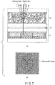
- FIG. 7 is a view for illustrating the operation of the display unit 10 in information display of a second example.
- the EL driving circuit 13 causes the first display panel 11 to display a color image.
- the entire area of the second display panel 12 is set in the scattered state (OFF state).
- the PN driving circuit 14 applies 0 V to all display electrodes 43 and the common electrode 44.
- the gradation in the scattered state is called "zero gradation".
- the light emitted from the first display panel 11 is scattered by the second display panel 12.
- the entirely of the display image of the display unit 10 becomes non-metallic display.
- FIG. 8 is a view for illustrating the operation of the display unit 10 in information display of a third example.
- the EL driving circuit 13 causes the first display panel 11 to display a color image.
- the entire area of the second display panel 12 is set in halftone.
- the halftone represents a state between the full gradation (transmissive state) and the zero gradation (scattered state).
- the PN driving circuit 14 applies an intermediate voltage, which is lower than the positive voltage at the time of the full gradation and is higher than 0 V, to all display electrodes 43, and applies 0 V to the common electrode 44.
- the liquid crystal molecules are obliquely aligned as a whole.
- the light emitted from the first display panel 11 is weakly scattered by the second display panel 12.
- the entirely of the display image of the display unit 10 becomes generally weak metallic display.
- the degree of metallic display can freely be set by varying the voltage level at the time of the halftone.
- the electronic watch (electronic device) 1 includes the first display panel 11 composed of the organic EL display element; the second display panel 12 composed of the polymer dispersed liquid crystal element; the spacer 22 configured to keep the distance between the first display panel 11 and second display panel 12; and the air layer 21 which is provided between the first display panel 11 and second display panel 12 and is surrounded by the spacer 22.
- the first display panel includes the pixel electrodes 35 which are provided on the TFT substrate 30 and reflect light; the light-emission layers 36 which are provided on the pixel electrodes 35 and emit light; and the common electrode 37 which is provided on the opposite substrate 31 and is in contact with the light-emission layers 36.
- the second display panel 12 includes the polymer dispersed liquid crystal layer 42 filled between the lower substrate 40 and upper substrate 41; the display electrodes 43 provided on the lower substrate 40; and the common electrode 44 provided on the upper substrate 41.
- the opposite substrate 31 of the first display panel 11 is disposed in such a manner as to directly face the second display panel 12.
- the first display panel 11 since the first display panel 11 uses neither a retardation plate ( ⁇ /4 plate) nor a polarizer, the light emitted from the light-emission layer 36 is not partially absorbed by the polarizer. Thereby, the brightness of the display unit 10 can be enhanced.
- the second display panel 12 does not require a polarizer. Thereby, the brightness of the display unit 10 can be enhanced.
- the second display panel 12 can perform the character display by using outside light. Thereby, the power consumption of the electronic watch 1 can be reduced.
- the first display panel 11 performs the information display
- the second display panel 12 can be set in the full-area transmissive state.
- the metallic display can be effected by the reflective metal which the first display panel 11 includes.
- halftone between the metallic display and non-metallic display can be displayed by varying the level of the transmissive state, that is, the gradation, of the second display panel 12.
- the electronic watch 1 according to the present embodiment can realize a plurality of kinds of display modes.
- the display mode of the electronic watch 1 can be switched, based on an operation of a touch sensor by a user.
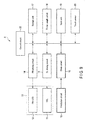
- FIG. 9 is a block diagram of an electronic watch 1 according to the second embodiment of the present invention.
- the electronic watch 1 further includes a touch sensor 50.
- the touch sensor 50 detects that the user has pressed the screen of the electronic watch 1, and further specifies a pressed position, i.e. the coordinates of a tap position.
- the detection method of the touch sensor 50 may be any one of a resistive film type, an electrostatic capacitance type, an electromagnetic induction method, a surface acoustic wave type, an infrared scanning method, and the like.
- the touch sensor 50 includes a touch panel 51.
- FIG. 10 is a cross-sectional view of the display unit 10 including the touch panel 51.
- FIG. 10 illustrates a configuration example of the touch panel 51 which adopts an electrostatic capacitance type.
- the touch panel 51 is provided on the display surface side of the second display panel 12.
- the touch panel 51 includes a transparent substrate (e.g. a glass substrate) 52.
- a plurality of transparent electrodes 53 having a desired sensor pattern are provided on the transparent substrate 52.
- the transparent substrate 52 and transparent electrodes 53 are attached to the second display panel 12 by using a transparent adhesive 54.
- FIG. 11 is a flowchart for illustrating the operation of the electronic watch 1.
- the electronic watch 1 performs character display (step S100). Specifically, the PN driving circuit 14 causes the second display panel (LCD) 12 to perform character display. The EL driving circuit 13 turns off the first display panel (OEL) 11.
- step S101 if the touch panel 51 was tapped once, the electronic watch 1 performs information display and non-metallic display (step S102). Specifically, the PN driving circuit 14 sets the second display panel 12 to a full-area zero gradation. Thereby, the second display panel 12 is set in a full-area scattered state. The EL driving circuit 13 causes the first display panel 11 to perform information display.
- step S103 if the touch panel 51 was tapped once again, the electronic watch 1 performs information display and halftone (1 gradation) display (step S104). Specifically, the PN driving circuit 14 sets the second display panel 12 to a full-area 1-gradation. Thereby, the entire area of the second display panel 12 is set in a slightly scattered state. The EL driving circuit 13 causes the first display panel 11 to perform information display.
- step S105 if the touch panel 51 was tapped once again, the electronic watch 1 performs information display and metallic display (step S106). For example, it is assumed that a 2-gradation is a full gradation.
- the PN driving circuit 14 sets the second display panel 12 to a full-area 2-gradation. Thereby, the second display panel 12 is set in a full-area transmissive state.
- the EL driving circuit 13 causes the first display panel 11 to perform information display.
- two or more levels of the halftone may be provided.
- the switching of the level of the halftone is also performed by the touch panel 51.
- the touch sensor 50 monitors whether the touch panel 51 was tapped once again (step S107). Subsequently, the touch sensor 50 monitors whether the touch panel 51 was further tapped once again (i.e. whether the touch panel 51 was successively tapped twice) (step S108).
- step S108 No
- one of the display modes can be selected and executed in accordance with the operation by the user.
- the three-color light-emission method was described by way of example as the organic EL display element, but other light-emission methods may be used.
- a color conversion method or a color filter method may be used.
- the color conversion method is a method in which an organic EL element that emits blue light is used and the blue light is converted to green light or red light by a fluorescence conversion layer.
- the color filter method is a method in which an organic EL element that emits white light is used and the white light is converted to RGB by filtering the white light by color filters.
- the display units according to the above-described embodiments are applicable to various electronic devices other than the electronic watch.
- the present invention is not limited to the above-mentioned embodiments, and can be reduced to practice by modifying the constituent elements without departing from the spirit and scope of the invention.
- the above-described embodiments include inventions of various stages, and a variety of inventions can be derived by properly combining structural elements of one embodiment or by properly combining structural elements of different embodiments. For example, if the object of the invention is achieved and the advantages of the invention are attained even after some of the structural elements disclosed in connection with the embodiments are deleted, the structure made up of the resultant structural elements can be extracted as an invention.
Landscapes
- Physics & Mathematics (AREA)
- Nonlinear Science (AREA)
- General Physics & Mathematics (AREA)
- Engineering & Computer Science (AREA)
- Chemical & Material Sciences (AREA)
- Crystallography & Structural Chemistry (AREA)
- Theoretical Computer Science (AREA)
- Optics & Photonics (AREA)
- Mathematical Physics (AREA)
- Computer Hardware Design (AREA)
- Human Computer Interaction (AREA)
- General Engineering & Computer Science (AREA)
- Geometry (AREA)
- Dispersion Chemistry (AREA)
- Liquid Crystal (AREA)
- Electroluminescent Light Sources (AREA)
- Devices For Indicating Variable Information By Combining Individual Elements (AREA)
Applications Claiming Priority (2)
| Application Number | Priority Date | Filing Date | Title |
|---|---|---|---|
| JP2017125082A JP2019008200A (ja) | 2017-06-27 | 2017-06-27 | 電子機器 |
| PCT/JP2018/021726 WO2019003839A1 (ja) | 2017-06-27 | 2018-06-06 | 電子機器 |
Publications (2)
| Publication Number | Publication Date |
|---|---|
| EP3648085A1 true EP3648085A1 (de) | 2020-05-06 |
| EP3648085A4 EP3648085A4 (de) | 2021-03-17 |
Family
ID=64741416
Family Applications (1)
| Application Number | Title | Priority Date | Filing Date |
|---|---|---|---|
| EP18825219.1A Ceased EP3648085A4 (de) | 2017-06-27 | 2018-06-06 | Elektronische vorrichtung |
Country Status (6)
| Country | Link |
|---|---|
| US (1) | US20200124917A1 (de) |
| EP (1) | EP3648085A4 (de) |
| JP (1) | JP2019008200A (de) |
| CN (1) | CN110800036A (de) |
| TW (1) | TWI684272B (de) |
| WO (1) | WO2019003839A1 (de) |
Families Citing this family (7)
| Publication number | Priority date | Publication date | Assignee | Title |
|---|---|---|---|---|
| JP6146594B1 (ja) * | 2015-12-22 | 2017-06-14 | カシオ計算機株式会社 | 表示装置及びその制御方法、制御プログラム |
| US10943959B1 (en) * | 2018-02-14 | 2021-03-09 | Apple Inc. | Display device with a light modulating layer |
| CN109765717B (zh) * | 2019-03-20 | 2021-01-22 | 京东方科技集团股份有限公司 | 像素结构及其驱动方法、阵列基板和显示装置 |
| US10996499B2 (en) * | 2019-08-09 | 2021-05-04 | Keith Rosenblum | Variably reflective display systems and methods |
| JP7593032B2 (ja) * | 2020-09-29 | 2024-12-03 | 株式会社レゾナック | 電荷輸送性ポリマー、電荷輸送性材料、インク組成物、有機層、有機エレクトロニクス素子、有機エレクトロルミネセンス素子、照明装置、表示素子、及び表示装置 |
| TWI757898B (zh) * | 2020-09-30 | 2022-03-11 | 宏碁股份有限公司 | 像素結構與使用其的顯示裝置 |
| JP7322101B2 (ja) * | 2021-07-02 | 2023-08-07 | シャープディスプレイテクノロジー株式会社 | 液晶表示装置 |
Family Cites Families (16)
| Publication number | Priority date | Publication date | Assignee | Title |
|---|---|---|---|---|
| JP4479140B2 (ja) * | 2001-09-21 | 2010-06-09 | セイコーエプソン株式会社 | 電子機器 |
| US7973749B2 (en) * | 2006-01-31 | 2011-07-05 | Nec Lcd Technologies, Ltd. | Display device, terminal device, and display panel |
| JP2007232882A (ja) * | 2006-02-28 | 2007-09-13 | Casio Comput Co Ltd | 表示装置及び電子機器 |
| US20120256895A1 (en) * | 2009-12-28 | 2012-10-11 | Sharp Kabushiki Kaisha | Display device |
| US8487835B2 (en) * | 2010-04-27 | 2013-07-16 | Sukho JUNG | Display device |
| WO2012004922A1 (ja) * | 2010-07-08 | 2012-01-12 | シャープ株式会社 | 液晶表示システム及び液晶表示システムの制御方法 |
| KR20130088686A (ko) * | 2012-01-31 | 2013-08-08 | 삼성전자주식회사 | 디스플레이 장치, 디스플레이 패널 및 디스플레이 방법 |
| KR101660657B1 (ko) * | 2013-02-04 | 2016-09-27 | 가부시키가이샤 오루투스 테크놀로지 | 액정 표시 장치 |
| JP2014153380A (ja) * | 2013-02-05 | 2014-08-25 | Pioneer Electronic Corp | 表示装置 |
| KR102354883B1 (ko) * | 2013-11-18 | 2022-01-25 | 삼성전자주식회사 | 디스플레이 장치 및 그 제어 방법 |
| US10170030B2 (en) * | 2014-02-07 | 2019-01-01 | Samsung Electronics Company, Ltd. | Dual-mode display |
| US9989798B2 (en) * | 2014-06-27 | 2018-06-05 | Lg Display Co., Ltd. | Light controlling apparatus, method of fabricating the light controlling apparatus and transparent display device including the light controlling apparatus with transparent mode and light shielding mode |
| JP2016038581A (ja) * | 2014-08-08 | 2016-03-22 | 株式会社半導体エネルギー研究所 | 表示パネル、表示装置および表示装置の駆動方法 |
| EP2990860B1 (de) * | 2014-08-29 | 2018-06-13 | LG Display Co., Ltd. | Lichtsteuerungsvorrichtung und verfahren zur herstellung davon |
| JP6401650B2 (ja) * | 2015-03-31 | 2018-10-10 | 住友化学株式会社 | Oled表示装置及びその製造方法 |
| CN106611826B (zh) * | 2016-12-27 | 2018-11-09 | 深圳市华星光电技术有限公司 | 量子点彩膜显示面板及其制作方法 |
-
2017
- 2017-06-27 JP JP2017125082A patent/JP2019008200A/ja active Pending
-
2018
- 2018-06-06 WO PCT/JP2018/021726 patent/WO2019003839A1/ja not_active Ceased
- 2018-06-06 CN CN201880037032.5A patent/CN110800036A/zh active Pending
- 2018-06-06 EP EP18825219.1A patent/EP3648085A4/de not_active Ceased
- 2018-06-15 TW TW107120653A patent/TWI684272B/zh active
-
2019
- 2019-12-19 US US16/720,690 patent/US20200124917A1/en not_active Abandoned
Also Published As
| Publication number | Publication date |
|---|---|
| EP3648085A4 (de) | 2021-03-17 |
| US20200124917A1 (en) | 2020-04-23 |
| CN110800036A (zh) | 2020-02-14 |
| WO2019003839A1 (ja) | 2019-01-03 |
| JP2019008200A (ja) | 2019-01-17 |
| TWI684272B (zh) | 2020-02-01 |
| TW201907558A (zh) | 2019-02-16 |
Similar Documents
| Publication | Publication Date | Title |
|---|---|---|
| US20200124917A1 (en) | Electronic device | |
| US10025150B2 (en) | Liquid crystal display | |
| US9208709B2 (en) | Backlight for a display | |
| US9285647B2 (en) | TFT array substrate, E-paper display panel and method for manufacturing the same | |
| US20200064686A1 (en) | Display panel, driving method thereof, and display device | |
| CN104977754A (zh) | 一种显示面板、显示装置及其控制方法 | |
| US10451931B2 (en) | Transflective display panel and transflective display device | |
| US10269328B2 (en) | Display panel including reflective pixels and self-display pixels and driving method thereof, display apparatus | |
| WO2013097443A1 (zh) | 显示面板、显示装置及显示装置的驱动方法 | |
| US20200117045A1 (en) | Liquid crystal display panel and pixel structure thereof and liquid crystal display device | |
| CN212255968U (zh) | 液晶显示面板及液晶显示装置 | |
| WO2011125271A1 (ja) | 表示装置、液晶モジュール及び画像表示システム | |
| CN107179638B (zh) | 一种显示面板及其控制方法、显示装置 | |
| US20260020487A1 (en) | Display panel, manufacturing method therefor and display apparatus | |
| US20200249528A1 (en) | Area light source module and control method therefor, and display device | |
| CN105467712A (zh) | 显示基板和显示装置 | |
| WO2021189274A1 (zh) | 触摸基板及触摸显示装置 | |
| CN107463032B (zh) | 液晶显示面板与显示装置 | |
| US20190064616A1 (en) | Transflective liquid crystal display | |
| KR20180063799A (ko) | 반사형 액정 표시 장치 | |
| KR102295609B1 (ko) | 도광패널 및 이를 포함하는 투명 디스플레이 | |
| CN104078010B (zh) | 显示设备和电子设备 | |
| CN107608565B (zh) | 触控显示面板及触控显示装置 | |
| KR20070071807A (ko) | 액정표시장치 및 그 구동방법 | |
| KR20120019307A (ko) | 액정표시장치 |
Legal Events
| Date | Code | Title | Description |
|---|---|---|---|
| STAA | Information on the status of an ep patent application or granted ep patent |
Free format text: STATUS: THE INTERNATIONAL PUBLICATION HAS BEEN MADE |
|
| PUAI | Public reference made under article 153(3) epc to a published international application that has entered the european phase |
Free format text: ORIGINAL CODE: 0009012 |
|
| STAA | Information on the status of an ep patent application or granted ep patent |
Free format text: STATUS: REQUEST FOR EXAMINATION WAS MADE |
|
| 17P | Request for examination filed |
Effective date: 20191227 |
|
| AK | Designated contracting states |
Kind code of ref document: A1 Designated state(s): AL AT BE BG CH CY CZ DE DK EE ES FI FR GB GR HR HU IE IS IT LI LT LU LV MC MK MT NL NO PL PT RO RS SE SI SK SM TR |
|
| AX | Request for extension of the european patent |
Extension state: BA ME |
|
| DAV | Request for validation of the european patent (deleted) | ||
| DAX | Request for extension of the european patent (deleted) | ||
| A4 | Supplementary search report drawn up and despatched |
Effective date: 20210216 |
|
| RIC1 | Information provided on ipc code assigned before grant |
Ipc: G09F 9/30 20060101ALI20210210BHEP Ipc: G09G 3/20 20060101ALI20210210BHEP Ipc: G09F 9/46 20060101AFI20210210BHEP Ipc: G02F 1/133 20060101ALI20210210BHEP Ipc: G02F 1/13 20060101ALI20210210BHEP |
|
| STAA | Information on the status of an ep patent application or granted ep patent |
Free format text: STATUS: EXAMINATION IS IN PROGRESS |
|
| 17Q | First examination report despatched |
Effective date: 20221220 |
|
| REG | Reference to a national code |
Ref country code: DE Ref legal event code: R003 |
|
| STAA | Information on the status of an ep patent application or granted ep patent |
Free format text: STATUS: THE APPLICATION HAS BEEN REFUSED |
|
| 18R | Application refused |
Effective date: 20250402 |