EP3650926B1 - Procédé de réparation d'un panneau d'affichage - Google Patents
Procédé de réparation d'un panneau d'affichage Download PDFInfo
- Publication number
- EP3650926B1 EP3650926B1 EP18800821.3A EP18800821A EP3650926B1 EP 3650926 B1 EP3650926 B1 EP 3650926B1 EP 18800821 A EP18800821 A EP 18800821A EP 3650926 B1 EP3650926 B1 EP 3650926B1
- Authority
- EP
- European Patent Office
- Prior art keywords
- filter film
- color filter
- laser
- bright spot
- repair region
- Prior art date
- Legal status (The legal status is an assumption and is not a legal conclusion. Google has not performed a legal analysis and makes no representation as to the accuracy of the status listed.)
- Active
Links
Images

Classifications
-
- G—PHYSICS
- G02—OPTICS
- G02F—OPTICAL DEVICES OR ARRANGEMENTS FOR THE CONTROL OF LIGHT BY MODIFICATION OF THE OPTICAL PROPERTIES OF THE MEDIA OF THE ELEMENTS INVOLVED THEREIN; NON-LINEAR OPTICS; FREQUENCY-CHANGING OF LIGHT; OPTICAL LOGIC ELEMENTS; OPTICAL ANALOGUE/DIGITAL CONVERTERS
- G02F1/00—Devices or arrangements for the control of the intensity, colour, phase, polarisation or direction of light arriving from an independent light source, e.g. switching, gating or modulating; Non-linear optics
- G02F1/01—Devices or arrangements for the control of the intensity, colour, phase, polarisation or direction of light arriving from an independent light source, e.g. switching, gating or modulating; Non-linear optics for the control of the intensity, phase, polarisation or colour
- G02F1/13—Devices or arrangements for the control of the intensity, colour, phase, polarisation or direction of light arriving from an independent light source, e.g. switching, gating or modulating; Non-linear optics for the control of the intensity, phase, polarisation or colour based on liquid crystals, e.g. single liquid crystal display cells
- G02F1/1306—Details
- G02F1/1309—Repairing; Testing
-
- G—PHYSICS
- G02—OPTICS
- G02F—OPTICAL DEVICES OR ARRANGEMENTS FOR THE CONTROL OF LIGHT BY MODIFICATION OF THE OPTICAL PROPERTIES OF THE MEDIA OF THE ELEMENTS INVOLVED THEREIN; NON-LINEAR OPTICS; FREQUENCY-CHANGING OF LIGHT; OPTICAL LOGIC ELEMENTS; OPTICAL ANALOGUE/DIGITAL CONVERTERS
- G02F1/00—Devices or arrangements for the control of the intensity, colour, phase, polarisation or direction of light arriving from an independent light source, e.g. switching, gating or modulating; Non-linear optics
- G02F1/01—Devices or arrangements for the control of the intensity, colour, phase, polarisation or direction of light arriving from an independent light source, e.g. switching, gating or modulating; Non-linear optics for the control of the intensity, phase, polarisation or colour
- G02F1/13—Devices or arrangements for the control of the intensity, colour, phase, polarisation or direction of light arriving from an independent light source, e.g. switching, gating or modulating; Non-linear optics for the control of the intensity, phase, polarisation or colour based on liquid crystals, e.g. single liquid crystal display cells
- G02F1/133—Constructional arrangements; Operation of liquid crystal cells; Circuit arrangements
- G02F1/1333—Constructional arrangements; Manufacturing methods
- G02F1/1335—Structural association of cells with optical devices, e.g. polarisers or reflectors
- G02F1/133509—Filters, e.g. light shielding masks
- G02F1/133512—Light shielding layers, e.g. black matrix
-
- G—PHYSICS
- G02—OPTICS
- G02F—OPTICAL DEVICES OR ARRANGEMENTS FOR THE CONTROL OF LIGHT BY MODIFICATION OF THE OPTICAL PROPERTIES OF THE MEDIA OF THE ELEMENTS INVOLVED THEREIN; NON-LINEAR OPTICS; FREQUENCY-CHANGING OF LIGHT; OPTICAL LOGIC ELEMENTS; OPTICAL ANALOGUE/DIGITAL CONVERTERS
- G02F1/00—Devices or arrangements for the control of the intensity, colour, phase, polarisation or direction of light arriving from an independent light source, e.g. switching, gating or modulating; Non-linear optics
- G02F1/01—Devices or arrangements for the control of the intensity, colour, phase, polarisation or direction of light arriving from an independent light source, e.g. switching, gating or modulating; Non-linear optics for the control of the intensity, phase, polarisation or colour
- G02F1/13—Devices or arrangements for the control of the intensity, colour, phase, polarisation or direction of light arriving from an independent light source, e.g. switching, gating or modulating; Non-linear optics for the control of the intensity, phase, polarisation or colour based on liquid crystals, e.g. single liquid crystal display cells
- G02F1/133—Constructional arrangements; Operation of liquid crystal cells; Circuit arrangements
- G02F1/1333—Constructional arrangements; Manufacturing methods
- G02F1/1335—Structural association of cells with optical devices, e.g. polarisers or reflectors
- G02F1/133509—Filters, e.g. light shielding masks
- G02F1/133514—Colour filters
-
- G—PHYSICS
- G02—OPTICS
- G02F—OPTICAL DEVICES OR ARRANGEMENTS FOR THE CONTROL OF LIGHT BY MODIFICATION OF THE OPTICAL PROPERTIES OF THE MEDIA OF THE ELEMENTS INVOLVED THEREIN; NON-LINEAR OPTICS; FREQUENCY-CHANGING OF LIGHT; OPTICAL LOGIC ELEMENTS; OPTICAL ANALOGUE/DIGITAL CONVERTERS
- G02F1/00—Devices or arrangements for the control of the intensity, colour, phase, polarisation or direction of light arriving from an independent light source, e.g. switching, gating or modulating; Non-linear optics
- G02F1/01—Devices or arrangements for the control of the intensity, colour, phase, polarisation or direction of light arriving from an independent light source, e.g. switching, gating or modulating; Non-linear optics for the control of the intensity, phase, polarisation or colour
- G02F1/13—Devices or arrangements for the control of the intensity, colour, phase, polarisation or direction of light arriving from an independent light source, e.g. switching, gating or modulating; Non-linear optics for the control of the intensity, phase, polarisation or colour based on liquid crystals, e.g. single liquid crystal display cells
- G02F1/133—Constructional arrangements; Operation of liquid crystal cells; Circuit arrangements
- G02F1/1333—Constructional arrangements; Manufacturing methods
- G02F1/1335—Structural association of cells with optical devices, e.g. polarisers or reflectors
- G02F1/133509—Filters, e.g. light shielding masks
- G02F1/133514—Colour filters
- G02F1/133516—Methods for their manufacture, e.g. printing, electro-deposition or photolithography
Definitions
- the present disclosure relates to the field of display panel repair technologies, and specifically to a method for repairing a display panel and a display panel
- the KR20170037726A provides a liquid crystal display device and a repairing method thereof, capable of effectively repairing a bright defect.
- the repairing method includes a step of providing the liquid crystal display device including a substrate, a light shielding member arranged on the substrate, an overcoat layer which is arranged on the substrate and the light shielding member and includes a material absorbing a wavelength of 200 nm to 400 nm; and a first laser irradiation step to form a micro cavity between the substrate and the overcoat layer by emitting a laser with the wavelength of 200 nm to 400 nm to the overcoat layer on the substrate.
- KR20070031141A provides a method for repairing an liquid crystal cell. By irradiating a laser to a predetermined region of the substrate where the luminescent point defect has occurred and the predetermined region is blackened, the luminescent point is darkened and the bright spot defect is eliminated.
- US2009141231A1 provides method for repairing a defective cell of a liquid crystal panel, which includes: providing a liquid crystal panel including an upper array substrate with a black matrix and a pigment layer formed thereon, a lower array substrate with a thin film transistor and attached with the upper array substrate, and a liquid crystal layer formed between the upper and lower substrates and including a plurality of cells; forming a certain gap between the black matrix and the upper array substrate by irradiating laser to a defective cell region among the plurality of cells in the liquid crystal panel; forming a comb-like structure with a certain gap between its teeth between the pigment layer and the upper array substrate by irradiating laser to the defective cell region; processing the black matrix by irradiating laser to the defective cell region to generate black matrix particles; and dispersing the black matrix particles between the pigment layer and the upper array substrate.
- CN102650750A provides a highlight maintaining method for a liquid crystal display.
- a color diaphragm plate of the liquid crystal display is maintained and comprises a base plate as well as a black matrix and red-green-blue color diaphragms arranged on the base plate, wherein red-green-blue color diaphragms are separated by the black matrix, and laser is utilized for implementing the following steps of: ageing the color diaphragms of sub pixel points to be maintained and the black matrix at the peripheries of the sub pixel points; forming seams between the color diaphragms and a glass base plate; granulating the black matrixes at the peripheries of the color diaphragms to generate black particles; and dispersing the black particles at the peripheries of the color diaphragms into the seams.
- the highlight maintaining method is applied to the improvement of the highlight maintenance.
- An embodiment of the present disclosure proposes a method for repairing a display panel, the display panel comprising a plurality of pixels for display, each of the pixels including a color filter film on a substrate, at least part of the pixels having a bright spot defect, the bright spot defect being a constantly bright spot within a single pixel region, the method comprising: determining a pixel where the bright spot defect resides and a position of the bright spot defect in the pixel; setting a repair region, the repair region being a region in the pixel including the bright spot defect and having an area smaller than that of the single pixel region; forming a black material layer in the repair region for preventing light emitted from a directly-below portion thereof from leaving a display surface of the display panel.
- the step of forming a black material layer in the repair region includes: performing carbonization treatment on the color filter film in the repair region by laser.
- the method further includes: performing modification treatment on the color filter film in the repair region by laser prior to performing carbonization treatment on the color filter film in the repair region.
- the parameters of the laser for the modification treatment include: a wavelength of 349 nm, an energy of 200 to 400 nJ, an operating rate of 150 to 300 ⁇ m/s, and a frequency of 40 to 60 Hz, wherein the operating rate is a traveling speed of a laser device.
- parameters of the laser for the carbonization treatment include: for red and green filter films, a wavelength of 446 nm, an energy of 1050 to 1350 nJ, and an operating rate of 60 to 80 ⁇ m/s; for a blue filter film, a wavelength of 446 nm, an energy of 1350 to 1590 nJ, and an operating rate of 60 to 80 ⁇ m/s.
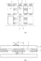
- an embodiment of the present disclosure not falling within the scope of the claimed invention, provides a method for repairing a bright spot defect 8 in a display panel wherein the display panel comprises a plurality of pixels 1 for performing display, and each of the pixels 1 has a color filter film 2 on a substrate 9. At least part of the pixels 1 have a bright spot defect 8, and the bright spot defect 8 is a constantly bright spot in the pixel 1.
- the method according to this embodiment is used for repairing the bright spot defect 8 in the display panel.
- the display panel to which it is applicable has a plurality of pixels 1 for display and each of the pixels 1 is provided with a color filter film 2 of a respective color.
- the bright spot defect 8 refers to a partial area in the pixel 1 which always emits light when the display panel is operating. This partial area of the pixel 1 can emit light, but cannot emit light according to the brightness that should be displayed or the desired brightness. For example, the partial area of the pixel 1 may always maintain certain brightness, or the brightness thereof may have a deviation from the brightness that should be displayed, so that the bright spot defect 8 is a constantly bright spot.
- the above bright spot defect 8 is only located in a partial area of the pixel 1, that is, the size of a single bright spot defect 8 should be smaller than the pixel 1, and regions other than the bright spot defect 8 in the pixel 1 can still be normally displayed.
- the bright spot defect 8 in each drawing only schematically indicates its position, and does not represent the shape of the bright spot defect 8, nor does it mean that the bright spot defect 8 is between two substrates.
- the above display panel includes a liquid crystal display panel.
- the bright spot defect 8 is usually caused by particles in the display panel.
- the liquid crystal display panel achieves display by liquid crystal deflection, but the presence of particles affects the liquid crystal deflection, so the liquid crystal display surface is most likely to suffer from a bright spot defect 8.
- the method proposed by an embodiment of the present disclosure may also be applied to repair the bright spot defect 8 in other types of display panels.
- the method for repairing a display panel comprises the following steps.
- a pixel 1 having a bright spot defect 8 can be found by a detecting means such as microscopic observation, and the position of the bright spot defect 8 in the pixel 1 can be determined.
- the repair region 11 is a region in the pixel 1 including the bright spot defect 8, but the repair region 11 does not include the entire area of the pixel 1, that is, a partial area of the pixel 1 does not belong to the repair region 11.
- a repair region 11 is determined in the pixel 1 that has the bright spot defect 8, and the repair region 11 needs to include the bright spot defect 8 therein, but does not occupy the entire pixel 1. That is, a part of the pixel 1 does not belong to the repair region 11.
- the repair region 11 may be slightly larger than the bright spot defect 8, and has a regular shape such as a rectangle.
- the above steps merely detect and determine the bright spot defect 8 in the pixel 1 and set the repair region 11 for the pixel 1 according to the bright spot defect 8, but do not involve actual operations on the display panel.
- the color filter film 2 in the repair region 11 is converted into black by a certain means, so that light cannot be emitted from the repair region 11, that is, light at the bright spot defect 8 cannot be emitted out, thereby finishing the repair.
- the color filter film 2 to which the position of the bright spot defect 8 corresponds is converted into black, so that light at the bright spot defect 8 cannot be emitted out, thus the region in the pixel corresponding to the bright spot defect 8 will not emit light. That is, the black filter film will prevent light emitted from a directly-below portion thereof from leaving the display surface of the display panel. Since the human eyes are insensitive to a dark object, the repaired position (i.e., the pixel region corresponding to the bright spot defect 8) is usually not noticed.
- the plurality of pixels 1 in the display panel are spaced apart from each other, and a black matrix 3 is disposed between color filter films 2 to which adjacent pixels 1 correspond.
- the repair region 11 is set such that at least one side thereof is connected to the black matrix 3.
- a plurality of pixels 1 in a display panel are spaced apart from each other at an interval, and the interval is not for display but for arrangement of driving structures such as a lead.
- a black matrix 3 for blocking light needs to be disposed at the interval, and the black matrix 3 is located between color filter films 2 to which adjacent pixels 1 correspond, thus a side of the color filter film 2 is adjacent to the black matrix 3.
- the black matrix 3 and the adjacent color filter film 2 may also have overlapping portions, but in this case, the black matrix 3 is still located between color filter films 2 to which adjacent pixels 1 correspond.
- the repair region 11 is connected to the black matrix 3, that is, the repair region 11 extends to the edge of the pixel 1, rather than being in the middle of the pixel 1 in isolation.
- step S013 may include the following steps.
- S103-1 Aging treatment is performed on the color filter film 2 in the repair region 11 and the black matrix 3 connected to the repair region 11 by laser.
- the color filter film 2 in the repair region 11 and the black matrix 3 connected to the repair region 11 may be irradiated with laser so that they are preheated and aged, making them more suitable for subsequent steps.
- parameters of the laser for irradiating the color filter film 2 in the repair region 11 and the black matrix 3 connected to the repair region 11 are: wavelength: 349 nm; energy: 200 to 400 nJ; operating rate: 150 to 300 ⁇ m/s; frequency: 40 to 60Hz.
- parameters of the laser for irradiating the color filter film in the repair region and the black matrix connected to the repair region are: wavelength: 349 nm; energy: 350 nJ; operating rate: 200 ⁇ m/s; frequency: 50 Hz.
- exemplary values of the wavelength of the laser are mentioned herein, for example, 349 nm, light having other wavelength parameters is also possible, and no limitation is imposed on the wavelength parameters of the laser in the present invention.
- different energies may also be obtained for laser sources having the same wavelength parameter.
- the laser parameters in embodiments of the present disclosure are particularly suitable for processing a partial area of the pixel 1. If the pixel 1 is to be processed as a whole, the laser parameters to be used are necessarily different.
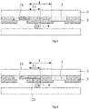
- the black matrix 3 connected to the repair region 11 is partially granulated by laser to form black matrix particles 31.
- the black matrix 3 connected to the repair region 11 is irradiated with laser to destroy the action of molecular bonds therein, so that part of the black matrix 3 (such as the black matrix 3 close to the substrate 9) is converted into black particles (black matrix particles 31).
- parameters of the laser for granulating the black matrix 3 are: wavelength: 349 nm; energy: 200 to 400 nJ; operating rate: 150 to 300 ⁇ m/s; frequency: 40 to 60 Hz.
- parameters of the laser for granulating the black matrix 3 are: wavelength: 349 nm; energy: 350 nJ; operating rate: 200 ⁇ m/s; frequency: 50 Hz.
- a gap 21 is generated between the color filter film 2 in the repair region 11 and the substrate 9 by laser.
- the color filter film 2 in the repair region 11 is irradiated with laser to cause minute shrinkage, thereby generating a gap 21 between the color filter film 2 and the substrate 9.
- parameters of the laser for generating a gap between the color filter film and the substrate are: for a red filter film, wavelength: 349 nm; energy: 1035 to 1125 nJ; operating rate: 60 to 80 ⁇ m/s; frequency :40 to 60 Hz; for a green filter film, wavelength: 349 nm; energy: 765 to 855 nJ; operating rate: 60 to 80 ⁇ m/s; frequency: 40 to 70 Hz; for a blue filter film, wavelength: 349 nm; energy: 540 to 810 nJ; operating rate: 70 to 90 ⁇ m/s; frequency: 50 to 70 Hz.
- the laser parameters described above are: for a red filter film, wavelength: 349 nm; energy: 1080 nJ; operating rate: 70 ⁇ m/s; frequency: 53 Hz; for a green filter film, wavelength: 349 nm; energy: 810 nJ; operating rate: 70 ⁇ m/s; frequency: 45 Hz; for a blue filter film, wavelength: 349 nm; energy: 770 nJ; operating rate: 80 ⁇ m/s; frequency: 60 Hz.
- the color filter films 2 of different colors may have different laser parameter ranges.
- step S103-3 of generating a gap 21 between the color filter film 2 and the substrate 9 and the step (step S103-2) of partially granulating the black matrix 3 do not have a necessary sequence relationship, but in order to avoid the occurrence of bubbles, the step of granulating the black matrix may be performed first, followed by the step of generating a gap 21.
- the black matrix particles 31 are separated from other portions of the black matrix 3, so that they can move freely into the gap 21 between the color filter film 2 and the substrate 9, thereby making the color filter film 2 of the repair region 11 convert into black.
- the black matrix 3 not granulated still remains between the pixels 1.
- the amount of black matrix particles 31 can be determined based on the size of the repair region 11. If the black matrix particles 31 are insufficient to fill the gap 21 of the entire repair region 11, the black matrix may continue to be granulated.
- the black matrix particles 31 in the gap 21 are uniformly diffused by laser.
- the black matrix particles 31 may fall into the gap 21 by themselves, but the distribution thereof is not necessarily uniform, and the entire repair region 11 may be not well covered. Therefore, the black matrix particles 31 in the gap 21 can be guided to move by laser irradiation (the black matrix particles may move following the movement of laser), so that they are diffused uniformly throughout the gap 21.
- Parameters of the laser for uniformly diffusing the black matrix particles in the gap include: wavelength: 349 nm; energy: 650 to 675 nJ; operating rate: 100 to 150 ⁇ m/s; frequency: 40 to 60 Hz.
- parameters of the laser for uniformly diffusing the black matrix particles in the gap are: wavelength: 349 nm; energy: 660 nJ; operating rate: 120 ⁇ m/s; frequency: 50 Hz.
- converting the color filter film 2 in the repair region 11 into black may include the following steps. S203-1 Modification treatment is performed on the color filter film 2 in the repair region 11 by laser.
- the color filter film 2 in the repair region 11 is irradiated with laser to change its molecular structure and improve its heat resistance, making it suitable for subsequent carbonization treatment.
- parameters of the laser for performing modification treatment on the color filter film 2 in the repair region 11 are: wavelength: 349 nm; energy: 200 to 400 nJ; operating rate: 150 to 300 ⁇ m/s; frequency: 40 to 60 Hz.
- parameters of the laser for performing modification treatment on the color filter film in the repair region are: wavelength: 349 nm; energy: 350 nJ; operating rate: 200 ⁇ m/s; frequency: 50 Hz.
- the color filter film 2 in the repair region 11 is irradiated with laser and directly carbonized to form a carbonized color filter film 22. Since the carbon is black, the carbonized color filter film 22 is directly black. This is equivalent to converting the color filter film 2 in the repair region 11 into black.
- the above laser parameters are: for red and green filter films, wavelength: 446 nm; energy: 1050 to 1350 nJ; operating rate: 60 to 80 ⁇ m/s; for a blue filter film, wavelength: 446 nm; energy: 1350 to 1590 nJ; operating rate: 60 to 80 ⁇ m/s.
- parameters of the laser for directly carbonizing the color filter film to form the carbonized color filter film 22 are: for red and green filter films, wavelength: 446 nm; energy: 1200 nJ; operating rate: 70 ⁇ m/s; for a blue filter film, wavelength: 446 nm; energy: 1500 nJ; operating rate: 70 ⁇ m/s.
- the color filter film 2 is directly carbonized and blackened, thereby achieving the purpose of converting the color filter film 2 in the repair region 11 into black. Therefore, in this embodiment, only the color filter film 2 in the repair region 11 is subjected to treatment, without the need to perform treatment on the black matrix 3.
- a further embodiment of the present disclosure provides a display panel that has been repaired by the method for repairing a bright spot defect in a display panel as described above.
- the display panel should have had a bright spot defect, and the color filter film in a partial area around the bright spot defect thereof has been converted into black by methods such as granulation of the black matrix, carbonization, and the like, so that the repair is finished.
- This embodiment provides a display device including the display panel described above.
- the display device may be any product or component having a display function, such as an electronic paper, a mobile phone, a tablet computer, a television, a display, a notebook computer, a digital photo frame, a navigator, and the like.
- a display function such as an electronic paper, a mobile phone, a tablet computer, a television, a display, a notebook computer, a digital photo frame, a navigator, and the like.
Landscapes
- Physics & Mathematics (AREA)
- Nonlinear Science (AREA)
- Chemical & Material Sciences (AREA)
- Crystallography & Structural Chemistry (AREA)
- General Physics & Mathematics (AREA)
- Optics & Photonics (AREA)
- Mathematical Physics (AREA)
- Engineering & Computer Science (AREA)
- Manufacturing & Machinery (AREA)
- Devices For Indicating Variable Information By Combining Individual Elements (AREA)
- Optical Filters (AREA)
- Liquid Crystal (AREA)
Claims (2)
- Procédé de réparation d'un panneau d'affichage, le panneau d'affichage comprenant une pluralité de pixels (1) pour l'affichage, chacun des pixels (1) comportant un film de filtre coloré (2) sur un substrat (9), au moins une partie des pixels (1) ayant un défaut de point lumineux (8), le défaut de point lumineux (8) étant un point lumineux constant dans une région d'un seul pixel, dans lequel le procédé comprend :la détermination d'un pixel (1) où se situe le défaut de point lumineux (8) et une position du défaut de point lumineux (8) dans le pixel (1) ;l'établissement d'une région de réparation (11), la région de réparation (11) étant une région dans le pixel (1) comportant le défaut de point lumineux (8) et ayant une surface plus petite que celle de la région d'un seul pixel ; etla formation d'une couche de matériau noir dans la région de réparation (11) pour empêcher la lumière émise par une partie directement au-dessous de celle-ci de quitter une surface d'affichage du panneau d'affichage ;dans lequel la formation d'une couche de matériau noir dans la région de réparation (11) comprend : la réalisation d'un traitement de carbonisation sur le film de filtre coloré (2) dans la région de réparation (11) par laser, de telle sorte que le film de filtre coloré (2) soit irradié par le laser et directement carbonisé pour former un film de filtre coloré carbonisé (22) ;caractérisé en ce que le procédé comprend en outre : l'exécution d'un traitement de modification sur le film de filtre coloré (2) dans la région de réparation (11) par laser avant d'effectuer un traitement de carbonisation sur le film de filtre coloré (2) dans la région de réparation (11) ;et dans lequel les paramètres du laser pour le traitement de modification comprennent : une longueur d'onde de 349 nm, une énergie de 200 à 400 nJ, un taux de fonctionnement de 150 à 300 µm/s, et une fréquence de 40 à 60 Hz, dans lequel la vitesse de fonctionnement est une vitesse de déplacement d'un dispositif laser.
- Procédé selon la revendication 1, caractérisé en ce que les paramètres du laser pour le traitement de carbonisation comprennent :
pour les films de filtres rouges et verts, une longueur d'onde de 446 nm, une énergie de 1 050 à 1 350 nJ et un taux de fonctionnement de 60 à 80 µm/s ; pour un film de filtre bleu, une longueur d'onde de 446 nm, une énergie de 1 350 à 1 590 nJ et un taux de fonctionnement de 60 à 80 µm/s.
Applications Claiming Priority (2)
| Application Number | Priority Date | Filing Date | Title |
|---|---|---|---|
| CN201710549833.7A CN109212791A (zh) | 2017-07-07 | 2017-07-07 | 显示面板、显示面板亮点不良的修复方法 |
| PCT/CN2018/080181 WO2019007107A1 (fr) | 2017-07-07 | 2018-03-23 | Procédé de réparation d'un panneau d'affichage et panneau d'affichage |
Publications (3)
| Publication Number | Publication Date |
|---|---|
| EP3650926A1 EP3650926A1 (fr) | 2020-05-13 |
| EP3650926A4 EP3650926A4 (fr) | 2021-03-17 |
| EP3650926B1 true EP3650926B1 (fr) | 2022-12-14 |
Family
ID=64949681
Family Applications (1)
| Application Number | Title | Priority Date | Filing Date |
|---|---|---|---|
| EP18800821.3A Active EP3650926B1 (fr) | 2017-07-07 | 2018-03-23 | Procédé de réparation d'un panneau d'affichage |
Country Status (5)
| Country | Link |
|---|---|
| US (1) | US11237415B2 (fr) |
| EP (1) | EP3650926B1 (fr) |
| JP (1) | JP7256012B2 (fr) |
| CN (1) | CN109212791A (fr) |
| WO (1) | WO2019007107A1 (fr) |
Families Citing this family (6)
| Publication number | Priority date | Publication date | Assignee | Title |
|---|---|---|---|---|
| TWI692744B (zh) * | 2019-01-25 | 2020-05-01 | 友達光電股份有限公司 | 顯示面板 |
| CN111292300B (zh) * | 2020-01-21 | 2023-09-01 | 京东方科技集团股份有限公司 | 显示面板的亮点不良的检测方法和设备、可读存储介质 |
| CN111983860B (zh) * | 2020-08-10 | 2022-07-29 | 深圳市华星光电半导体显示技术有限公司 | 显示面板和显示装置 |
| CN114300516B (zh) | 2021-12-23 | 2024-11-26 | 武汉华星光电半导体显示技术有限公司 | Oled显示面板及其激光修复方法 |
| CN115172421A (zh) * | 2022-06-30 | 2022-10-11 | 合肥维信诺科技有限公司 | 显示面板、显示装置、修补方法以及修补装置 |
| CN119300678A (zh) * | 2024-10-18 | 2025-01-10 | 京东方科技集团股份有限公司 | 显示面板的修复方法和修复装置 |
Family Cites Families (17)
| Publication number | Priority date | Publication date | Assignee | Title |
|---|---|---|---|---|
| US7636148B2 (en) | 2004-12-14 | 2009-12-22 | Lg Display Co., Ltd. | Apparatus and method for repairing liquid crystal display device |
| KR101232136B1 (ko) | 2005-09-14 | 2013-02-12 | 엘지디스플레이 주식회사 | 액정셀의 휘점불량을 리페어하는 방법, 그 방법을 이용한액정표시소자의 제조방법, 및 그 방법에 의해 리페어된액정표시소자 |
| KR20080065748A (ko) | 2007-01-10 | 2008-07-15 | 참앤씨(주) | 액정표시패널의 리페어 방법 및 장치 |
| KR100879010B1 (ko) * | 2007-06-18 | 2009-01-15 | 주식회사 코윈디에스티 | 표시장치의 휘점불량 수리방법 |
| KR101060472B1 (ko) * | 2007-11-30 | 2011-08-29 | 엘지디스플레이 주식회사 | 액정표시패널의 불량셀 리페어방법 |
| TWI430000B (zh) * | 2010-07-02 | 2014-03-11 | Ind Tech Res Inst | 平面顯示器之修補方法與系統 |
| JP5733065B2 (ja) * | 2011-07-07 | 2015-06-10 | 三菱電機株式会社 | 液晶表示パネルとその修復方法 |
| CN102650750B (zh) * | 2011-09-22 | 2014-06-11 | 京东方科技集团股份有限公司 | 液晶显示器亮点维修方法 |
| CN102629004B (zh) * | 2012-03-05 | 2014-08-06 | 京东方科技集团股份有限公司 | 一种液晶显示器亮点维修方法 |
| CN102654661B (zh) * | 2012-05-04 | 2015-01-21 | 京东方科技集团股份有限公司 | 液晶显示面板的修复方法 |
| KR101931736B1 (ko) * | 2012-07-31 | 2018-12-26 | 삼성디스플레이 주식회사 | 터치 스크린 패널 일체형 표시장치 |
| JP6327735B2 (ja) | 2013-03-18 | 2018-05-23 | 株式会社ブイ・テクノロジー | 液晶表示パネルの輝点欠陥除去方法及び装置 |
| DE102015003193A1 (de) * | 2015-03-12 | 2016-09-15 | Siltectra Gmbh | Vorrichtung und Verfahren zum kontinuierlichen Behandeln eines Festkörpers mittels Laserstrahlen |
| CN105068304B (zh) * | 2015-09-14 | 2018-06-01 | 武汉华星光电技术有限公司 | 彩膜基板及其制作方法 |
| KR102499179B1 (ko) * | 2015-09-25 | 2023-02-10 | 티씨엘 차이나 스타 옵토일렉트로닉스 테크놀로지 컴퍼니 리미티드 | 액정 표시 장치 및 그 리페어 방법 |
| CN105182592B (zh) * | 2015-10-29 | 2019-01-04 | 武汉华星光电技术有限公司 | 一种显示面板 |
| KR20200104981A (ko) * | 2019-02-27 | 2020-09-07 | 삼성디스플레이 주식회사 | 표시 장치 및 그 리페어 방법 |
-
2017
- 2017-07-07 CN CN201710549833.7A patent/CN109212791A/zh active Pending
-
2018
- 2018-03-23 US US16/303,735 patent/US11237415B2/en active Active
- 2018-03-23 WO PCT/CN2018/080181 patent/WO2019007107A1/fr not_active Ceased
- 2018-03-23 EP EP18800821.3A patent/EP3650926B1/fr active Active
- 2018-03-23 JP JP2018562334A patent/JP7256012B2/ja active Active
Also Published As
| Publication number | Publication date |
|---|---|
| EP3650926A4 (fr) | 2021-03-17 |
| CN109212791A (zh) | 2019-01-15 |
| JP2020526779A (ja) | 2020-08-31 |
| JP7256012B2 (ja) | 2023-04-11 |
| EP3650926A1 (fr) | 2020-05-13 |
| US11237415B2 (en) | 2022-02-01 |
| WO2019007107A1 (fr) | 2019-01-10 |
| US20210223582A1 (en) | 2021-07-22 |
Similar Documents
| Publication | Publication Date | Title |
|---|---|---|
| EP3650926B1 (fr) | Procédé de réparation d'un panneau d'affichage | |
| TWI395000B (zh) | 平面顯示面板及其亮點修補方法 | |
| US10012862B2 (en) | Method for manufacturing liquid crystal cell, liquid crystal cell, and display device | |
| CN102636904A (zh) | 彩色滤光片、彩色滤光片的制作方法及液晶面板 | |
| CN108766995B (zh) | 显示面板和显示装置 | |
| CN102650750B (zh) | 液晶显示器亮点维修方法 | |
| TW201227057A (en) | Method of repairing display device and repiared structure thereof | |
| CN202008564U (zh) | 液晶面板 | |
| KR20150026910A (ko) | 디스플레이 장치 | |
| US20130052902A1 (en) | Method of repairing a display panel and apparatus for performing the same | |
| US10634967B2 (en) | Display device, brightness defect correction method for display device, and brightness defect correction device for display device | |
| US20110299020A1 (en) | Liquid crystal display device and method of manufacturing same | |
| US9057895B2 (en) | Liquid crystal display panel and repair method thereof | |
| JP2008152256A (ja) | 液晶ディスプレイパネルの修復方法 | |
| US10705371B2 (en) | Color filter substrate, manufacturing method thereof, display panel, manufacturing method thereof and bright spot defect correction method thereof, and display apparatus | |
| CN102854647A (zh) | 一种修复显示面板亮点像素瑕疵的方法以及显示面板 | |
| CN102629004B (zh) | 一种液晶显示器亮点维修方法 | |
| CN102955289B (zh) | 一种彩膜基板及其制作方法、显示面板、显示装置 | |
| CN101510016B (zh) | 平面显示面板与光电装置及其亮点修补方法 | |
| WO2016086452A1 (fr) | Procédé de fabrication de filtre de couleur, filtre de couleur et panneau à cristaux liquides | |
| US20060087613A1 (en) | Liquid crystal display, and method for repairing defective pixels of liquid crystal display | |
| JP2013047720A (ja) | カラーフィルタおよびカラーフィルタの製造方法 | |
| KR100839031B1 (ko) | 평판 디스플레이 패널의 리페어 방법 | |
| JP2021012363A (ja) | 液晶パネルの製造方法および液晶パネルの製造装置 | |
| US7692739B2 (en) | Liquid crystal panel and method of repairing same |
Legal Events
| Date | Code | Title | Description |
|---|---|---|---|
| STAA | Information on the status of an ep patent application or granted ep patent |
Free format text: STATUS: UNKNOWN |
|
| STAA | Information on the status of an ep patent application or granted ep patent |
Free format text: STATUS: THE INTERNATIONAL PUBLICATION HAS BEEN MADE |
|
| PUAI | Public reference made under article 153(3) epc to a published international application that has entered the european phase |
Free format text: ORIGINAL CODE: 0009012 |
|
| STAA | Information on the status of an ep patent application or granted ep patent |
Free format text: STATUS: REQUEST FOR EXAMINATION WAS MADE |
|
| 17P | Request for examination filed |
Effective date: 20200127 |
|
| AK | Designated contracting states |
Kind code of ref document: A1 Designated state(s): AL AT BE BG CH CY CZ DE DK EE ES FI FR GB GR HR HU IE IS IT LI LT LU LV MC MK MT NL NO PL PT RO RS SE SI SK SM TR |
|
| AX | Request for extension of the european patent |
Extension state: BA ME |
|
| DAV | Request for validation of the european patent (deleted) | ||
| DAX | Request for extension of the european patent (deleted) | ||
| R17P | Request for examination filed (corrected) |
Effective date: 20200127 |
|
| A4 | Supplementary search report drawn up and despatched |
Effective date: 20210212 |
|
| RIC1 | Information provided on ipc code assigned before grant |
Ipc: G02F 1/1335 20060101ALI20210208BHEP Ipc: G02F 1/13 20060101AFI20210208BHEP |
|
| RIC1 | Information provided on ipc code assigned before grant |
Ipc: G02F 1/1335 20060101ALI20220620BHEP Ipc: G02F 1/13 20060101AFI20220620BHEP |
|
| GRAP | Despatch of communication of intention to grant a patent |
Free format text: ORIGINAL CODE: EPIDOSNIGR1 |
|
| STAA | Information on the status of an ep patent application or granted ep patent |
Free format text: STATUS: GRANT OF PATENT IS INTENDED |
|
| INTG | Intention to grant announced |
Effective date: 20220810 |
|
| GRAS | Grant fee paid |
Free format text: ORIGINAL CODE: EPIDOSNIGR3 |
|
| GRAA | (expected) grant |
Free format text: ORIGINAL CODE: 0009210 |
|
| STAA | Information on the status of an ep patent application or granted ep patent |
Free format text: STATUS: THE PATENT HAS BEEN GRANTED |
|
| AK | Designated contracting states |
Kind code of ref document: B1 Designated state(s): AL AT BE BG CH CY CZ DE DK EE ES FI FR GB GR HR HU IE IS IT LI LT LU LV MC MK MT NL NO PL PT RO RS SE SI SK SM TR |
|
| REG | Reference to a national code |
Ref country code: GB Ref legal event code: FG4D |
|
| REG | Reference to a national code |
Ref country code: CH Ref legal event code: EP |
|
| REG | Reference to a national code |
Ref country code: DE Ref legal event code: R096 Ref document number: 602018044304 Country of ref document: DE |
|
| REG | Reference to a national code |
Ref country code: IE Ref legal event code: FG4D |
|
| REG | Reference to a national code |
Ref country code: AT Ref legal event code: REF Ref document number: 1538043 Country of ref document: AT Kind code of ref document: T Effective date: 20230115 |
|
| REG | Reference to a national code |
Ref country code: LT Ref legal event code: MG9D |
|
| REG | Reference to a national code |
Ref country code: NL Ref legal event code: MP Effective date: 20221214 |
|
| PG25 | Lapsed in a contracting state [announced via postgrant information from national office to epo] |
Ref country code: SE Free format text: LAPSE BECAUSE OF FAILURE TO SUBMIT A TRANSLATION OF THE DESCRIPTION OR TO PAY THE FEE WITHIN THE PRESCRIBED TIME-LIMIT Effective date: 20221214 Ref country code: NO Free format text: LAPSE BECAUSE OF FAILURE TO SUBMIT A TRANSLATION OF THE DESCRIPTION OR TO PAY THE FEE WITHIN THE PRESCRIBED TIME-LIMIT Effective date: 20230314 Ref country code: LT Free format text: LAPSE BECAUSE OF FAILURE TO SUBMIT A TRANSLATION OF THE DESCRIPTION OR TO PAY THE FEE WITHIN THE PRESCRIBED TIME-LIMIT Effective date: 20221214 Ref country code: FI Free format text: LAPSE BECAUSE OF FAILURE TO SUBMIT A TRANSLATION OF THE DESCRIPTION OR TO PAY THE FEE WITHIN THE PRESCRIBED TIME-LIMIT Effective date: 20221214 |
|
| REG | Reference to a national code |
Ref country code: AT Ref legal event code: MK05 Ref document number: 1538043 Country of ref document: AT Kind code of ref document: T Effective date: 20221214 |
|
| PG25 | Lapsed in a contracting state [announced via postgrant information from national office to epo] |
Ref country code: RS Free format text: LAPSE BECAUSE OF FAILURE TO SUBMIT A TRANSLATION OF THE DESCRIPTION OR TO PAY THE FEE WITHIN THE PRESCRIBED TIME-LIMIT Effective date: 20221214 Ref country code: LV Free format text: LAPSE BECAUSE OF FAILURE TO SUBMIT A TRANSLATION OF THE DESCRIPTION OR TO PAY THE FEE WITHIN THE PRESCRIBED TIME-LIMIT Effective date: 20221214 Ref country code: HR Free format text: LAPSE BECAUSE OF FAILURE TO SUBMIT A TRANSLATION OF THE DESCRIPTION OR TO PAY THE FEE WITHIN THE PRESCRIBED TIME-LIMIT Effective date: 20221214 Ref country code: GR Free format text: LAPSE BECAUSE OF FAILURE TO SUBMIT A TRANSLATION OF THE DESCRIPTION OR TO PAY THE FEE WITHIN THE PRESCRIBED TIME-LIMIT Effective date: 20230315 |
|
| PG25 | Lapsed in a contracting state [announced via postgrant information from national office to epo] |
Ref country code: NL Free format text: LAPSE BECAUSE OF FAILURE TO SUBMIT A TRANSLATION OF THE DESCRIPTION OR TO PAY THE FEE WITHIN THE PRESCRIBED TIME-LIMIT Effective date: 20221214 |
|
| PG25 | Lapsed in a contracting state [announced via postgrant information from national office to epo] |
Ref country code: SM Free format text: LAPSE BECAUSE OF FAILURE TO SUBMIT A TRANSLATION OF THE DESCRIPTION OR TO PAY THE FEE WITHIN THE PRESCRIBED TIME-LIMIT Effective date: 20221214 Ref country code: RO Free format text: LAPSE BECAUSE OF FAILURE TO SUBMIT A TRANSLATION OF THE DESCRIPTION OR TO PAY THE FEE WITHIN THE PRESCRIBED TIME-LIMIT Effective date: 20221214 Ref country code: PT Free format text: LAPSE BECAUSE OF FAILURE TO SUBMIT A TRANSLATION OF THE DESCRIPTION OR TO PAY THE FEE WITHIN THE PRESCRIBED TIME-LIMIT Effective date: 20230414 Ref country code: ES Free format text: LAPSE BECAUSE OF FAILURE TO SUBMIT A TRANSLATION OF THE DESCRIPTION OR TO PAY THE FEE WITHIN THE PRESCRIBED TIME-LIMIT Effective date: 20221214 Ref country code: EE Free format text: LAPSE BECAUSE OF FAILURE TO SUBMIT A TRANSLATION OF THE DESCRIPTION OR TO PAY THE FEE WITHIN THE PRESCRIBED TIME-LIMIT Effective date: 20221214 Ref country code: CZ Free format text: LAPSE BECAUSE OF FAILURE TO SUBMIT A TRANSLATION OF THE DESCRIPTION OR TO PAY THE FEE WITHIN THE PRESCRIBED TIME-LIMIT Effective date: 20221214 Ref country code: AT Free format text: LAPSE BECAUSE OF FAILURE TO SUBMIT A TRANSLATION OF THE DESCRIPTION OR TO PAY THE FEE WITHIN THE PRESCRIBED TIME-LIMIT Effective date: 20221214 |
|
| PG25 | Lapsed in a contracting state [announced via postgrant information from national office to epo] |
Ref country code: SK Free format text: LAPSE BECAUSE OF FAILURE TO SUBMIT A TRANSLATION OF THE DESCRIPTION OR TO PAY THE FEE WITHIN THE PRESCRIBED TIME-LIMIT Effective date: 20221214 Ref country code: PL Free format text: LAPSE BECAUSE OF FAILURE TO SUBMIT A TRANSLATION OF THE DESCRIPTION OR TO PAY THE FEE WITHIN THE PRESCRIBED TIME-LIMIT Effective date: 20221214 Ref country code: IS Free format text: LAPSE BECAUSE OF FAILURE TO SUBMIT A TRANSLATION OF THE DESCRIPTION OR TO PAY THE FEE WITHIN THE PRESCRIBED TIME-LIMIT Effective date: 20230414 Ref country code: AL Free format text: LAPSE BECAUSE OF FAILURE TO SUBMIT A TRANSLATION OF THE DESCRIPTION OR TO PAY THE FEE WITHIN THE PRESCRIBED TIME-LIMIT Effective date: 20221214 |
|
| REG | Reference to a national code |
Ref country code: DE Ref legal event code: R097 Ref document number: 602018044304 Country of ref document: DE |
|
| PLBE | No opposition filed within time limit |
Free format text: ORIGINAL CODE: 0009261 |
|
| STAA | Information on the status of an ep patent application or granted ep patent |
Free format text: STATUS: NO OPPOSITION FILED WITHIN TIME LIMIT |
|
| PG25 | Lapsed in a contracting state [announced via postgrant information from national office to epo] |
Ref country code: MC Free format text: LAPSE BECAUSE OF FAILURE TO SUBMIT A TRANSLATION OF THE DESCRIPTION OR TO PAY THE FEE WITHIN THE PRESCRIBED TIME-LIMIT Effective date: 20221214 Ref country code: DK Free format text: LAPSE BECAUSE OF FAILURE TO SUBMIT A TRANSLATION OF THE DESCRIPTION OR TO PAY THE FEE WITHIN THE PRESCRIBED TIME-LIMIT Effective date: 20221214 |
|
| REG | Reference to a national code |
Ref country code: CH Ref legal event code: PL |
|
| 26N | No opposition filed |
Effective date: 20230915 |
|
| GBPC | Gb: european patent ceased through non-payment of renewal fee |
Effective date: 20230323 |
|
| PG25 | Lapsed in a contracting state [announced via postgrant information from national office to epo] |
Ref country code: SI Free format text: LAPSE BECAUSE OF FAILURE TO SUBMIT A TRANSLATION OF THE DESCRIPTION OR TO PAY THE FEE WITHIN THE PRESCRIBED TIME-LIMIT Effective date: 20221214 |
|
| REG | Reference to a national code |
Ref country code: BE Ref legal event code: MM Effective date: 20230331 |
|
| PG25 | Lapsed in a contracting state [announced via postgrant information from national office to epo] |
Ref country code: LU Free format text: LAPSE BECAUSE OF NON-PAYMENT OF DUE FEES Effective date: 20230323 |
|
| REG | Reference to a national code |
Ref country code: IE Ref legal event code: MM4A |
|
| PG25 | Lapsed in a contracting state [announced via postgrant information from national office to epo] |
Ref country code: GB Free format text: LAPSE BECAUSE OF NON-PAYMENT OF DUE FEES Effective date: 20230323 |
|
| PG25 | Lapsed in a contracting state [announced via postgrant information from national office to epo] |
Ref country code: LI Free format text: LAPSE BECAUSE OF NON-PAYMENT OF DUE FEES Effective date: 20230331 Ref country code: IE Free format text: LAPSE BECAUSE OF NON-PAYMENT OF DUE FEES Effective date: 20230323 Ref country code: GB Free format text: LAPSE BECAUSE OF NON-PAYMENT OF DUE FEES Effective date: 20230323 Ref country code: FR Free format text: LAPSE BECAUSE OF NON-PAYMENT OF DUE FEES Effective date: 20230331 Ref country code: CH Free format text: LAPSE BECAUSE OF NON-PAYMENT OF DUE FEES Effective date: 20230331 |
|
| PG25 | Lapsed in a contracting state [announced via postgrant information from national office to epo] |
Ref country code: BE Free format text: LAPSE BECAUSE OF NON-PAYMENT OF DUE FEES Effective date: 20230331 |
|
| PG25 | Lapsed in a contracting state [announced via postgrant information from national office to epo] |
Ref country code: IT Free format text: LAPSE BECAUSE OF FAILURE TO SUBMIT A TRANSLATION OF THE DESCRIPTION OR TO PAY THE FEE WITHIN THE PRESCRIBED TIME-LIMIT Effective date: 20221214 |
|
| PG25 | Lapsed in a contracting state [announced via postgrant information from national office to epo] |
Ref country code: BG Free format text: LAPSE BECAUSE OF FAILURE TO SUBMIT A TRANSLATION OF THE DESCRIPTION OR TO PAY THE FEE WITHIN THE PRESCRIBED TIME-LIMIT Effective date: 20221214 |
|
| PG25 | Lapsed in a contracting state [announced via postgrant information from national office to epo] |
Ref country code: BG Free format text: LAPSE BECAUSE OF FAILURE TO SUBMIT A TRANSLATION OF THE DESCRIPTION OR TO PAY THE FEE WITHIN THE PRESCRIBED TIME-LIMIT Effective date: 20221214 |
|
| PG25 | Lapsed in a contracting state [announced via postgrant information from national office to epo] |
Ref country code: CY Free format text: LAPSE BECAUSE OF FAILURE TO SUBMIT A TRANSLATION OF THE DESCRIPTION OR TO PAY THE FEE WITHIN THE PRESCRIBED TIME-LIMIT; INVALID AB INITIO Effective date: 20180323 |
|
| PG25 | Lapsed in a contracting state [announced via postgrant information from national office to epo] |
Ref country code: HU Free format text: LAPSE BECAUSE OF FAILURE TO SUBMIT A TRANSLATION OF THE DESCRIPTION OR TO PAY THE FEE WITHIN THE PRESCRIBED TIME-LIMIT; INVALID AB INITIO Effective date: 20180323 |
|
| PG25 | Lapsed in a contracting state [announced via postgrant information from national office to epo] |
Ref country code: TR Free format text: LAPSE BECAUSE OF FAILURE TO SUBMIT A TRANSLATION OF THE DESCRIPTION OR TO PAY THE FEE WITHIN THE PRESCRIBED TIME-LIMIT Effective date: 20221214 |
|
| PGFP | Annual fee paid to national office [announced via postgrant information from national office to epo] |
Ref country code: DE Payment date: 20260319 Year of fee payment: 9 |