EP3650936A1 - Ébauche de photomasque réfléchissant et photomasque réfléchissant - Google Patents
Ébauche de photomasque réfléchissant et photomasque réfléchissant Download PDFInfo
- Publication number
- EP3650936A1 EP3650936A1 EP18828644.7A EP18828644A EP3650936A1 EP 3650936 A1 EP3650936 A1 EP 3650936A1 EP 18828644 A EP18828644 A EP 18828644A EP 3650936 A1 EP3650936 A1 EP 3650936A1
- Authority
- EP
- European Patent Office
- Prior art keywords
- film
- light absorbing
- reflective
- tin oxide
- reflective photomask
- Prior art date
- Legal status (The legal status is an assumption and is not a legal conclusion. Google has not performed a legal analysis and makes no representation as to the accuracy of the status listed.)
- Pending
Links
Images



Classifications
-
- G—PHYSICS
- G03—PHOTOGRAPHY; CINEMATOGRAPHY; ANALOGOUS TECHNIQUES USING WAVES OTHER THAN OPTICAL WAVES; ELECTROGRAPHY; HOLOGRAPHY
- G03F—PHOTOMECHANICAL PRODUCTION OF TEXTURED OR PATTERNED SURFACES, e.g. FOR PRINTING, FOR PROCESSING OF SEMICONDUCTOR DEVICES; MATERIALS THEREFOR; ORIGINALS THEREFOR; APPARATUS SPECIALLY ADAPTED THEREFOR
- G03F1/00—Originals for photomechanical production of textured or patterned surfaces, e.g., masks, photo-masks, reticles; Mask blanks or pellicles therefor; Containers specially adapted therefor; Preparation thereof
- G03F1/22—Masks or mask blanks for imaging by radiation of 100nm or shorter wavelength, e.g. X-ray masks, extreme ultraviolet [EUV] masks; Preparation thereof
-
- G—PHYSICS
- G03—PHOTOGRAPHY; CINEMATOGRAPHY; ANALOGOUS TECHNIQUES USING WAVES OTHER THAN OPTICAL WAVES; ELECTROGRAPHY; HOLOGRAPHY
- G03F—PHOTOMECHANICAL PRODUCTION OF TEXTURED OR PATTERNED SURFACES, e.g. FOR PRINTING, FOR PROCESSING OF SEMICONDUCTOR DEVICES; MATERIALS THEREFOR; ORIGINALS THEREFOR; APPARATUS SPECIALLY ADAPTED THEREFOR
- G03F1/00—Originals for photomechanical production of textured or patterned surfaces, e.g., masks, photo-masks, reticles; Mask blanks or pellicles therefor; Containers specially adapted therefor; Preparation thereof
- G03F1/22—Masks or mask blanks for imaging by radiation of 100nm or shorter wavelength, e.g. X-ray masks, extreme ultraviolet [EUV] masks; Preparation thereof
- G03F1/24—Reflection masks; Preparation thereof
-
- G—PHYSICS
- G03—PHOTOGRAPHY; CINEMATOGRAPHY; ANALOGOUS TECHNIQUES USING WAVES OTHER THAN OPTICAL WAVES; ELECTROGRAPHY; HOLOGRAPHY
- G03F—PHOTOMECHANICAL PRODUCTION OF TEXTURED OR PATTERNED SURFACES, e.g. FOR PRINTING, FOR PROCESSING OF SEMICONDUCTOR DEVICES; MATERIALS THEREFOR; ORIGINALS THEREFOR; APPARATUS SPECIALLY ADAPTED THEREFOR
- G03F1/00—Originals for photomechanical production of textured or patterned surfaces, e.g., masks, photo-masks, reticles; Mask blanks or pellicles therefor; Containers specially adapted therefor; Preparation thereof
- G03F1/38—Masks having auxiliary features, e.g. special coatings or marks for alignment or testing; Preparation thereof
- G03F1/48—Protective coatings
-
- G—PHYSICS
- G03—PHOTOGRAPHY; CINEMATOGRAPHY; ANALOGOUS TECHNIQUES USING WAVES OTHER THAN OPTICAL WAVES; ELECTROGRAPHY; HOLOGRAPHY
- G03F—PHOTOMECHANICAL PRODUCTION OF TEXTURED OR PATTERNED SURFACES, e.g. FOR PRINTING, FOR PROCESSING OF SEMICONDUCTOR DEVICES; MATERIALS THEREFOR; ORIGINALS THEREFOR; APPARATUS SPECIALLY ADAPTED THEREFOR
- G03F1/00—Originals for photomechanical production of textured or patterned surfaces, e.g., masks, photo-masks, reticles; Mask blanks or pellicles therefor; Containers specially adapted therefor; Preparation thereof
- G03F1/52—Reflectors
-
- G—PHYSICS
- G03—PHOTOGRAPHY; CINEMATOGRAPHY; ANALOGOUS TECHNIQUES USING WAVES OTHER THAN OPTICAL WAVES; ELECTROGRAPHY; HOLOGRAPHY
- G03F—PHOTOMECHANICAL PRODUCTION OF TEXTURED OR PATTERNED SURFACES, e.g. FOR PRINTING, FOR PROCESSING OF SEMICONDUCTOR DEVICES; MATERIALS THEREFOR; ORIGINALS THEREFOR; APPARATUS SPECIALLY ADAPTED THEREFOR
- G03F1/00—Originals for photomechanical production of textured or patterned surfaces, e.g., masks, photo-masks, reticles; Mask blanks or pellicles therefor; Containers specially adapted therefor; Preparation thereof
- G03F1/54—Absorbers, e.g. of opaque materials
-
- B—PERFORMING OPERATIONS; TRANSPORTING
- B82—NANOTECHNOLOGY
- B82Y—SPECIFIC USES OR APPLICATIONS OF NANOSTRUCTURES; MEASUREMENT OR ANALYSIS OF NANOSTRUCTURES; MANUFACTURE OR TREATMENT OF NANOSTRUCTURES
- B82Y10/00—Nanotechnology for information processing, storage or transmission, e.g. quantum computing or single electron logic
-
- B—PERFORMING OPERATIONS; TRANSPORTING
- B82—NANOTECHNOLOGY
- B82Y—SPECIFIC USES OR APPLICATIONS OF NANOSTRUCTURES; MEASUREMENT OR ANALYSIS OF NANOSTRUCTURES; MANUFACTURE OR TREATMENT OF NANOSTRUCTURES
- B82Y20/00—Nanooptics, e.g. quantum optics or photonic crystals
-
- B—PERFORMING OPERATIONS; TRANSPORTING
- B82—NANOTECHNOLOGY
- B82Y—SPECIFIC USES OR APPLICATIONS OF NANOSTRUCTURES; MEASUREMENT OR ANALYSIS OF NANOSTRUCTURES; MANUFACTURE OR TREATMENT OF NANOSTRUCTURES
- B82Y40/00—Manufacture or treatment of nanostructures
Definitions
- the present invention relates to a reflective photomask for use in lithography that uses extreme ultraviolet light as a light source, and to a reflective photomask blank for use in producing the reflective photomask.
- the minimum resolution size of a transfer pattern in the photolithography largely depends on the wavelength of an exposure light source and can be reduced as the wavelength decreases. Therefore, in order to realize further miniaturization of transfer patterns, exposure light sources are shifting from conventional ArF excimer lasers (wavelength 193 nm) to EUV (Extreme Ultra Violet) with a wavelength of 13.5 nm.
- the EUV is absorbed by most materials at high rates. Therefore, in the EUV lithography, it is not possible to use a refractive optical system that makes use of the transmission of light, and it is also not possible to use a transmissive photomask. Consequently, a reflective photomask is used as a photomask for EUV exposure (an EUV mask).
- PTL 1 discloses an EUV photomask obtained by forming a light reflective layer on a glass substrate, the light reflective layer composed of a multilayer film in which molybdenum (Mo) layers and silicon (Si) layers are alternately laminated, forming a light absorbing layer mainly containing tantalum (Ta) on the light reflective layer, and forming a pattern in the light absorbing layer.
- Mo molybdenum
- Si silicon
- EUV is made incident with its optical axis inclined at 6 degrees to the direction perpendicular to the EUV mask surface, and reflected light with its optical axis inclined at 6 degrees to the side opposite to the incident light is directed toward a semiconductor substrate.
- the incident light on the EUV mask since the optical axis is inclined, the incident light on the EUV mask generates a shadow of a mask pattern (a patterned light absorbing layer) of the EUV mask.
- the problem caused by the generation of the shadow is called the shadowing effect.
- the shadowing effect is the theoretical problem of the EUV lithography where the optical axis is inclined.
- a film having a film thickness of 60 to 90 nm and mainly containing tantalum (Ta) is used as a light absorbing layer.
- Ta tantalum
- EUV mask blanks and EUV masks are also required to improve the cleaning resistance of a light absorbing layer.
- a first aspect of the present invention is a reflective photomask blank for producing a reflective photomask for pattern transfer that uses light with a wavelength of an extreme ultraviolet region as a light source, the reflective photomask blank including: a substrate; a reflective layer formed on the substrate; and a light absorbing layer formed on the reflective layer.
- the light absorbing layer includes a tin oxide film with an atomic ratio (O/Sn) of oxygen (O) to tin (Sn) being more than 1.50 and equal to or less than 2.0, and with a film thickness of 25 nm or more and 45 nm or less.
- a second aspect of the present invention is a reflective photomask including a substrate; a reflective layer formed on the substrate; and a light absorbing pattern layer formed on the reflective layer and patterned, the light absorbing pattern layer including a tin oxide film with an atomic ratio (O/Sn) of oxygen (O) to tin (Sn) being more than 1.50 and equal to or less than 2.0, and with a film thickness of 25 nm or more and 45 nm or less.
- the shadowing effect of a reflective photomask for pattern transfer using extreme ultraviolet light as a light source is suppressed or reduced to improve the performance of transfer to a semiconductor substrate, and that the cleaning resistance of a light absorbing layer is improved.
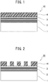
- a reflective photomask blank 10 of this embodiment includes a substrate 1, a reflective layer 2 formed on the substrate 1, a capping layer 3 formed on the reflective layer 2, and a light absorbing layer 4 formed on the capping layer 3.
- the light absorbing layer 4 is composed of a tin oxide film in which the atomic ratio (O/Sn) of oxygen (O) to tin (Sn) is more than 1.50 and equal to or less than 2.0 and which has a film thickness of 25 nm or more and 45 nm or less.
- a substrate made of low-expansion synthetic quartz or the like is used as the substrate 1.
- a reflective photomask 20 of this embodiment includes the substrate 1, the reflective layer 2 formed on the substrate 1, the capping layer 3 formed on the reflective layer 2, and a light absorbing pattern layer 41 formed on the capping layer 3.
- the light absorbing pattern layer 41 is composed of a tin oxide film in which the atomic ratio (O/Sn) of oxygen (O) to tin (Sn) is more than 1.50 and equal to or less than 2.0 and which has a film thickness of 25 nm or more and 45 nm or less.
- the light absorbing pattern layer 41 is formed by patterning the light absorbing layer 4 of the reflective photomask blank 10.
- a light absorbing layer (hereinafter also referred to simply as an "absorbing layer”) of a reflective photomask blank is dry-etched and formed into a predetermined exposure transfer pattern and serves to absorb irradiated EUV.
- the absorbing layer should be made thin.
- Ta tantalum
- the absorbency for EUV is not sufficient so that the reflectance in an absorbing layer region becomes high. Therefore, in order to simultaneously achieve the film thinning of the absorbing layer and its light absorbency for EUV, a material having higher light absorbency for EUV than the existing absorbing layer material is required.
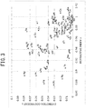
- FIG. 3 illustrates optical constants of metal materials at the wavelength of the EUV region, wherein the abscissa axis represents the refractive index n and the ordinate axis represents the extinction coefficient k.
- the abscissa axis represents the refractive index n and the ordinate axis represents the extinction coefficient k.
- the extinction coefficients of these materials are in a range from 0.07 to 0.08 and are about twice the extinction coefficient 0.041 of Ta which is the conventional absorbing layer material. That is, these materials have high light absorbency.
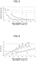
- a tin oxide film as a light absorbing layer of a reflective photomask blank and a reflective photomask. While a simple substance of Sn has a low melting point, around 230°C, and thus has a problem in thermal stability and cleaning resistance, the melting point can be significantly increased by using a tin oxide film. Actually, a plurality of tin oxide films with different O/Sn ratios was formed by reactive sputtering, and the melting points thereof were measured by a thermal analysis apparatus. As a result, as illustrated in FIG. 4 , it was found that the greater the O/Sn ratio, the higher the melting point.
- the cleaning was performed by three types of methods, i.e. SPM (sulfuric-acid and hydrogen-peroxide mixture) cleaning, APM (ammonium hydrogen-peroxide mixture) cleaning, and strong cleaning.
- SPM sulfuric-acid and hydrogen-peroxide mixture
- APM ammonium hydrogen-peroxide mixture
- the weight change of the sample before and after the cleaning was examined by measurement using an electronic analytical balance, and when there was a change in weight corresponding to a film thickness of 5 nm, it was determined that the film loss was "present".
- the tin oxide film in which the atomic ratio (O/Sn) of oxygen to tin is more than 1.50 and equal to or less than 2.0 can have sufficient resistance to heat at the time of producing a photomask or at the time of EUV exposure and sufficient resistance to a cleaning solution (acid or alkali) and ultrasonic cleaning in a megasonic band at the time of producing a photomask.
- the tin oxide film is chemically stable, it can be dry-etched with a chlorine-based gas and thus can be patterned.
- volatility of SnCl 4 which is a compound of Sn and Cl, is higher than that of a compound of a high absorption material other than Sn and Cl.
- Optical constants (extinction coefficient and refractive index) for EUV hardly differ between tin oxide with an O/Sn ratio of 1.5 to 2.0 and tin alone. Therefore, using a tin oxide film with the O/Sn ratio of 1.5 to 2.0 as a light absorbing layer of a reflective photomask blank and a reflective photomask, it is possible to maintain the same light absorbency as when a light absorbing layer is Sn alone.
- Rm is a reflected light intensity from a reflective layer region
- Ra is a reflected light intensity from a light absorbing layer region
- a capping layer protecting layer having a thickness of 2.5 nm and made of Ru was present under the absorbing layer
- 40 pairs of reflective layers each made of Si and Mo were present under the capping layer
- a flat substrate made of synthetic quartz was present under the reflective layers
- a conductive layer made of CrN was present on a back surface of the substrate
- the reflectance can be reduced to half or less with the same film thickness, and the film thickness can be reduced to half or less with the same reflectance.
- the tin oxide film is effective as a light absorbing film.
- a Ta film requires a thickness of at least 40 nm or more, while a tin oxide (SnO x ) film requires only about 17 nm. Therefore, it is seen that, also in terms of the OD, the tin oxide film is effective as a light absorbing film that can reduce the film thickness.
- the simulation conditions were such that the wavelength of a light source was set to 13.5 nm (EUV wavelength), NA was set to 0.33, the incident angle was set to 6 degrees, and a quasar was used for illumination.
- the HV bias value is a line width difference of a transferred pattern that depends on the orientation of a mask pattern, i.e. a difference between a line width in the H (Horizontal) direction and a line width in the V (Vertical) direction.
- the line width in the H direction represents a line width in a direction parallel to a plane formed by incident light and reflected light
- the line width in the V direction represents a line width in a direction perpendicular to a plane formed by incident light and reflected light.
- the horizontal pattern size is affected by the shadowing effect so that a reduction in contrast at an edge portion of a transferred pattern or a reduction in line width (Y-direction) thereof occurs. Since the pattern affected by the shadowing effect is reduced in line width after the transfer, the line width difference (i.e. HV bias) occurs between the vertical transferred pattern size and the horizontal transferred pattern size.
- a pattern used in this simulation is a mask pattern designed to have a size of 16-nm LS (Line and Space are 1:1) on a semiconductor substrate. Therefore, since 1/4 reduction projection exposure is usually used in the EUV lithography, the pattern size on an EUV mask is that of a 64-nm LS pattern. As illustrated in FIG. 7 , it is seen that the HV bias value of the transferred pattern increases as the film thickness of the absorbing layer increases, for each of the Ta film and the tin oxide film.
- the HV bias value is 10.5 nm, i.e. very large, with the Ta film, while the HV bias value is 3.3 nm with the tin oxide film so that it is significantly reduced and improved ( FIG. 8 ).
- the HV bias is 3.2 nm with the Ta film and 2.1 nm with the tin oxide film.
- HV bias the influence of the shadowing effect
- NILS Normalized Image Log Slope
- NILS is a characteristic value indicating an inclination between a light portion and a dark portion from a light intensity distribution of a transferred pattern. The greater the value, the better the pattern transfer properties (resolution, line edge roughness, etc.).
- NILS was evaluated by calculation (the same simulation as described above). The results are illustrated in FIG. 9 .
- NILS pattern contrast
- a graph of FIG. 10 illustrates the film thickness dependence of NILS (average of values in the X- and Y-directions) obtained by calculation (the same simulation as described above) in the case of a tin oxide film and a Ta film. From this figure, it is seen that the NILS decreases as the film thickness decreases, for each of the tin oxide film and the Ta film. The reason for this is that it is conjectured that when the absorbing film is thin, the reflectance in the absorbing film region becomes high to make the OD of a mask low, resulting in a reduction in NILS. Therefore, in order to obtain the value of NILS that is necessary for pattern transfer, a certain film thickness is required.
- a tin oxide film with a film thickness of 45 nm or less as a light absorbing layer of a reflective photomask blank and a reflective photomask, it is possible to increase the NILS (average of values in the X- and Y-directions) compared to the case where a Ta film is used.
- the optimum film thickness is approximately 45 nm or more, but the NILS does not exceed 1 with most of the film thicknesses equal to or more than 45 nm.
- a reflective photomask blank of a first aspect of the present invention and a reflective photomask of a second aspect of the present invention has a light absorbing layer including a tin oxide film with an atomic ratio (O/Sn) of oxygen (O) to tin (Sn) that is more than 1.50 and equal to or less than 2.0, and with a film thickness of 25 nm or more and 45 nm or less.
- O/Sn atomic ratio
- the light absorbing layer of the reflective photomask blank of the first aspect of the present invention and the reflective photomask of the second aspect of the present invention includes the tin oxide film with the film thickness of 25 nm or more and 45 nm or less, the influence of the shadowing effect can be made small compared to a reflective photomask blank and a reflective photomask having a light absorbing layer composed of a Ta film. As a result, high NILS (pattern contrast) is obtained so that an improvement in the resolution of a transferred pattern and a reduction in line edge roughness can be expected.
- NILS pattern contrast
- the film thickness of the tin oxide film is 25 nm or more and 45 nm or less, the influence of the shadowing effect can be made small compared to a reflective photomask blank and a reflective photomask having a light absorbing layer including a tin oxide film that does not satisfy the film thickness of 25 nm or more and 45 nm or less. Further, high cleaning resistance is ensured compared to a reflective photomask blank and a reflective photomask in which the atomic ratio (O/Sn) of a tin oxide film included in a light absorbing layer is 1.50 or less.
- a material forming the tin oxide film included in the light absorbing layer preferably contains 80 at% or more of tin (Sn) and oxygen (O) in total.
- a metal such as Si, In, Te, Ta, Pt, Cr, or Ru, or a light element such as nitrogen or carbon may be mixed according to the purpose.
- the tin oxide film by adding In to the tin oxide film, it is possible to impart conductivity to the film while ensuring the transparency, so that it is possible to enhance the inspectability in a mask pattern inspection using DUV light with a wavelength of 190 to 260 nm.
- nitrogen or carbon when nitrogen or carbon is mixed to the tin oxide film, it is possible to increase the etching rate in dry etching of the tin oxide film.
- the reflective photomask blank of the first aspect of the present invention and the reflective photomask of the second aspect of the present invention by having the light absorbing layer including the tin oxide film with the film thickness of 25 nm or more and 45 nm or less, the influence of the shadowing effect can be reduced so that high NILS can be obtained compared to the conventional product having the light absorbing layer composed of the Ta film. Therefore, it is possible to realize an improvement in the resolution of a transferred pattern and a reduction in line edge roughness. Further, since the X- and Y-direction NILSs approach each other, the HV bias value can be reduced so that a transferred pattern faithful to a mask pattern can be obtained.
- a reflective layer 12 of a multilayer structure composed of 40 pairs of Si and Mo (total film thickness 280 nm) was formed on a substrate 11 made of synthetic quartz, and a capping layer 13 composed of a Ru film was formed to a film thickness of 2.5 nm on the reflective layer 12. Then, a light absorbing layer 14 was formed on the capping layer 13. Then, a conductive layer 15 made of CrN was formed to a film thickness of 100 nm on a back surface of the substrate 11.
- the light absorbing layer 14 was formed in each of the samples by changing the material (Ta or tin oxide) and the film thickness as indicated in Table 2.
- the tin oxide film was formed so that the O/Sn ratio became 2.00 or 1.51.
- Each of the layers was formed using a sputtering apparatus.
- the tin oxide film was formed by a reactive sputtering method so that the O/Sn ratio became 2.00 or 1.51 by controlling the amount of oxygen introduced into a chamber during sputtering.
- the film thickness of each of the layers was measured by a transmission electron microscope, and the O/Sn ratio of the tin oxide film was measured by XPS (X-ray Photoelectron Spectroscopy).
- a positive chemically amplified resist (SEBP9012: manufactured by Shin-Etsu Chemical Co., Ltd.) was coated to a film thickness of 170 nm on the light absorbing layer 14 of the reflective photomask blank 100. Then, a predetermined pattern was written on this resist film using an electron beam writing apparatus (JBX3030: manufactured by Japan Electronics Co., Ltd.). Then, a prebaking treatment was performed at 110°C for 10 minutes, and then a developing treatment was performed using a spray developing apparatus (SFG3000: manufactured by Sigmameltec Ltd.). Consequently, as illustrated in FIG. 12 , a resist pattern 16 was formed on the light absorbing layer 14.
- SEBP9012 manufactured by Shin-Etsu Chemical Co., Ltd.
- the light absorbing layer 14 was made into a light absorbing pattern layer 141.
- each sample of a reflective photomask 200 was obtained in which the reflective layer 12 of the multilayer structure composed of the 40 pairs of Si and Mo (total film thickness 280 nm), the capping layer 13 composed of the 2.5-nm Ru film, and the light absorbing pattern layer 141 were formed in this order on the surface of the substrate 11 made of synthetic quartz, and the conductive layer 15 was formed on the back surface of the substrate 11 made of synthetic quartz.
- a pattern of the light absorbing pattern layer 141 was transferred to an EUV positive chemically amplified resist film formed on a wafer, by exposure using an EUV exposure apparatus (NXE3300B manufactured by ASML Inc.).
- the good results were obtained by using the reflective photomask having the SnO film with the O/Sn ratio of 2.00 or 1.51 and with the film thickness of 25 nm or more and 45 nm or less as the light absorbing layer. Further, when the reflective photomask having the SnO film with the O/Sn ratio of 2.00 or 1.51 and with the film thickness of 32 nm or more and 45 nm or less as the light absorbing layer was used, the line edge roughness was 3.4 nm or less, and therefore, it was found that the better results were obtained in this case.
Landscapes
- Physics & Mathematics (AREA)
- General Physics & Mathematics (AREA)
- Preparing Plates And Mask In Photomechanical Process (AREA)
- Exposure Of Semiconductors, Excluding Electron Or Ion Beam Exposure (AREA)
Applications Claiming Priority (2)
| Application Number | Priority Date | Filing Date | Title |
|---|---|---|---|
| JP2017132026 | 2017-07-05 | ||
| PCT/JP2018/024889 WO2019009211A1 (fr) | 2017-07-05 | 2018-06-29 | Ébauche de photomasque réfléchissant et photomasque réfléchissant |
Publications (2)
| Publication Number | Publication Date |
|---|---|
| EP3650936A1 true EP3650936A1 (fr) | 2020-05-13 |
| EP3650936A4 EP3650936A4 (fr) | 2020-09-09 |
Family
ID=64950081
Family Applications (1)
| Application Number | Title | Priority Date | Filing Date |
|---|---|---|---|
| EP18828644.7A Pending EP3650936A4 (fr) | 2017-07-05 | 2018-06-29 | Ébauche de photomasque réfléchissant et photomasque réfléchissant |
Country Status (8)
| Country | Link |
|---|---|
| US (1) | US11294270B2 (fr) |
| EP (1) | EP3650936A4 (fr) |
| JP (1) | JP6888675B2 (fr) |
| KR (1) | KR102666821B1 (fr) |
| CN (1) | CN110785703B (fr) |
| SG (1) | SG11201913845YA (fr) |
| TW (1) | TWI761546B (fr) |
| WO (1) | WO2019009211A1 (fr) |
Cited By (2)
| Publication number | Priority date | Publication date | Assignee | Title |
|---|---|---|---|---|
| EP4152093A4 (fr) * | 2020-05-14 | 2024-12-11 | Toppan Photomask Co., Ltd. | Ébauche de masque réfléchissant et masque réfléchissant |
| TWI916576B (zh) | 2021-06-02 | 2026-03-01 | 日商科盛德光罩股份有限公司 | 反射型空白光罩及反射型光罩 |
Families Citing this family (12)
| Publication number | Priority date | Publication date | Assignee | Title |
|---|---|---|---|---|
| WO2020184473A1 (fr) * | 2019-03-13 | 2020-09-17 | Hoya株式会社 | Ébauche de masque de type réflexion, masque de type réflexion et procédé pour le fabriquer, et procédé de fabrication de dispositif à semi-conducteur |
| KR102946015B1 (ko) * | 2019-10-29 | 2026-03-31 | 에이지씨 가부시키가이샤 | 반사형 마스크 블랭크 및 반사형 마스크 |
| JP7610346B2 (ja) * | 2019-11-01 | 2025-01-08 | テクセンドフォトマスク株式会社 | 反射型マスク及び反射型マスクの製造方法 |
| KR102511751B1 (ko) * | 2019-11-05 | 2023-03-21 | 주식회사 에스앤에스텍 | 극자외선 리소그래피용 블랭크마스크 및 포토마스크 |
| JP6919699B2 (ja) | 2019-11-28 | 2021-08-18 | 凸版印刷株式会社 | 反射型フォトマスクブランク及び反射型フォトマスク |
| JP7409861B2 (ja) * | 2019-12-18 | 2024-01-09 | 株式会社トッパンフォトマスク | 反射型マスクブランク、反射型マスク、反射型マスクの製造方法、及び反射型マスクの修正方法 |
| JP7354005B2 (ja) | 2020-02-12 | 2023-10-02 | Hoya株式会社 | 反射型マスクブランク、反射型マスク、及び半導体装置の製造方法 |
| KR20210155863A (ko) * | 2020-06-16 | 2021-12-24 | 삼성전자주식회사 | 극자외선 리소그래피용 위상 반전 마스크 및 이를 이용한 반도체 소자의 제조 방법 |
| JP7538050B2 (ja) * | 2021-01-08 | 2024-08-21 | 株式会社トッパンフォトマスク | 反射型フォトマスクブランク及び反射型フォトマスク |
| JP7614949B2 (ja) * | 2021-06-02 | 2025-01-16 | テクセンドフォトマスク株式会社 | 反射型フォトマスクブランク及び反射型フォトマスク |
| US12165913B2 (en) * | 2021-07-12 | 2024-12-10 | Changxin Memory Technologies, Inc. | Method for manufacturing semiconductor device and semiconductor device |
| KR102535171B1 (ko) * | 2021-11-04 | 2023-05-26 | 에스케이엔펄스 주식회사 | 블랭크 마스크 및 이를 이용한 포토마스크 |
Family Cites Families (7)
| Publication number | Priority date | Publication date | Assignee | Title |
|---|---|---|---|---|
| JP2005121908A (ja) * | 2003-10-16 | 2005-05-12 | Advanced Display Inc | 反射型液晶表示装置および半透過型液晶表示装置ならびにこれらの製法 |
| JP4802462B2 (ja) * | 2004-07-27 | 2011-10-26 | 三菱電機株式会社 | 薄膜トランジスタアレイ基板の製造方法 |
| JP5194888B2 (ja) * | 2007-09-27 | 2013-05-08 | 凸版印刷株式会社 | 反射型フォトマスクブランク及びその製造方法、反射型フォトマスク及びその製造方法並びに半導体素子の製造方法 |
| JP5332741B2 (ja) * | 2008-09-25 | 2013-11-06 | 凸版印刷株式会社 | 反射型フォトマスク |
| US8962220B2 (en) * | 2009-04-02 | 2015-02-24 | Toppan Printing Co., Ltd. | Reflective photomask and reflective photomask blank |
| JP5418293B2 (ja) | 2010-02-25 | 2014-02-19 | 凸版印刷株式会社 | 反射型フォトマスクおよび反射型フォトマスクブランクならびにその製造方法 |
| KR101727783B1 (ko) * | 2010-06-15 | 2017-04-17 | 칼 짜이스 에스엠테 게엠베하 | Euv 리소그래피를 위한 마스크, euv 리소그래피 시스템 그리고 마스크의 결상을 최적화하는 방법 |
-
2018
- 2018-06-29 JP JP2019527677A patent/JP6888675B2/ja active Active
- 2018-06-29 EP EP18828644.7A patent/EP3650936A4/fr active Pending
- 2018-06-29 CN CN201880042350.0A patent/CN110785703B/zh active Active
- 2018-06-29 KR KR1020197037791A patent/KR102666821B1/ko active Active
- 2018-06-29 SG SG11201913845YA patent/SG11201913845YA/en unknown
- 2018-06-29 US US16/626,290 patent/US11294270B2/en active Active
- 2018-06-29 WO PCT/JP2018/024889 patent/WO2019009211A1/fr not_active Ceased
- 2018-07-05 TW TW107123248A patent/TWI761546B/zh active
Cited By (4)
| Publication number | Priority date | Publication date | Assignee | Title |
|---|---|---|---|---|
| EP4152093A4 (fr) * | 2020-05-14 | 2024-12-11 | Toppan Photomask Co., Ltd. | Ébauche de masque réfléchissant et masque réfléchissant |
| EP4586012A3 (fr) * | 2020-05-14 | 2025-11-19 | Tekscend Photomask Corp. | Ébauche de masque réfléchissant et masque réfléchissant |
| US12510818B2 (en) | 2020-05-14 | 2025-12-30 | Tekscend Photomask Corp. | Reflective mask blank and reflective mask |
| TWI916576B (zh) | 2021-06-02 | 2026-03-01 | 日商科盛德光罩股份有限公司 | 反射型空白光罩及反射型光罩 |
Also Published As
| Publication number | Publication date |
|---|---|
| EP3650936A4 (fr) | 2020-09-09 |
| CN110785703A (zh) | 2020-02-11 |
| TW201907224A (zh) | 2019-02-16 |
| US20200159106A1 (en) | 2020-05-21 |
| TWI761546B (zh) | 2022-04-21 |
| US11294270B2 (en) | 2022-04-05 |
| CN110785703B (zh) | 2023-07-21 |
| KR20200018476A (ko) | 2020-02-19 |
| KR102666821B1 (ko) | 2024-05-16 |
| JP6888675B2 (ja) | 2021-06-16 |
| JPWO2019009211A1 (ja) | 2020-04-30 |
| WO2019009211A1 (fr) | 2019-01-10 |
| SG11201913845YA (en) | 2020-01-30 |
Similar Documents
| Publication | Publication Date | Title |
|---|---|---|
| US11294270B2 (en) | Reflective photomask blank and reflective photomask | |
| US11067886B2 (en) | Reflective photomask blank and reflective photomask | |
| EP3882698A1 (fr) | Ébauche de photomasque réfléchissant et photomasque réfléchissant | |
| US8435704B2 (en) | Mask blank, transfer mask, and methods of manufacturing the same | |
| EP3979000A1 (fr) | Ébauches de photomasque réfléchissant et photomasque réfléchissant | |
| US20140322634A1 (en) | Mask black, transfer mask, method of manufacturing a transfer mask, and method of manufacturing a semiconductor device | |
| JP2019139085A (ja) | 反射型フォトマスクブランク及び反射型フォトマスク | |
| EP4152093A1 (fr) | Ébauche de masque réfléchissant et masque réfléchissant | |
| EP4293422A1 (fr) | Ébauche de masque photographique réfléchissant et masque photographique réfléchissant | |
| EP4231094A1 (fr) | Masque réfléchissant et procédé de production de masque réfléchissant | |
| EP4067994A1 (fr) | Ébauche de photomasque réfléchissant et photomasque réfléchissant | |
| JP2019138971A (ja) | 反射型フォトマスクブランク及び反射型フォトマスク | |
| EP4053631A1 (fr) | Masque réfléchissant et procédé de production pour masque réfléchissant | |
| JP7553735B1 (ja) | 反射型フォトマスクブランク、反射型フォトマスク及び反射型フォトマスクの製造方法 | |
| EP4279990A1 (fr) | Ébauche de photomasque réfléchissant et photomasque réfléchissant | |
| WO2025216119A1 (fr) | Ébauche de photomasque réfléchissant, photomasque réfléchissant et procédé de fabrication de photomasque réfléchissant | |
| CN116500852A (zh) | 掩模胚料、转印用掩模及其制造方法、显示装置制造方法 |
Legal Events
| Date | Code | Title | Description |
|---|---|---|---|
| STAA | Information on the status of an ep patent application or granted ep patent |
Free format text: STATUS: THE INTERNATIONAL PUBLICATION HAS BEEN MADE |
|
| PUAI | Public reference made under article 153(3) epc to a published international application that has entered the european phase |
Free format text: ORIGINAL CODE: 0009012 |
|
| STAA | Information on the status of an ep patent application or granted ep patent |
Free format text: STATUS: REQUEST FOR EXAMINATION WAS MADE |
|
| 17P | Request for examination filed |
Effective date: 20200103 |
|
| AK | Designated contracting states |
Kind code of ref document: A1 Designated state(s): AL AT BE BG CH CY CZ DE DK EE ES FI FR GB GR HR HU IE IS IT LI LT LU LV MC MK MT NL NO PL PT RO RS SE SI SK SM TR |
|
| AX | Request for extension of the european patent |
Extension state: BA ME |
|
| A4 | Supplementary search report drawn up and despatched |
Effective date: 20200810 |
|
| RIC1 | Information provided on ipc code assigned before grant |
Ipc: G03F 1/24 20120101AFI20200804BHEP Ipc: B82Y 10/00 20110101ALI20200804BHEP Ipc: G03F 1/54 20120101ALI20200804BHEP Ipc: G03F 1/58 20120101ALI20200804BHEP Ipc: B82Y 40/00 20110101ALI20200804BHEP |
|
| DAV | Request for validation of the european patent (deleted) | ||
| DAX | Request for extension of the european patent (deleted) | ||
| RAP1 | Party data changed (applicant data changed or rights of an application transferred) |
Owner name: TOPPAN PHOTOMASK CO., LTD. |
|
| RAP3 | Party data changed (applicant data changed or rights of an application transferred) |
Owner name: TEKSCEND PHOTOMASK CORP. |
|
| STAA | Information on the status of an ep patent application or granted ep patent |
Free format text: STATUS: EXAMINATION IS IN PROGRESS |
|
| 17Q | First examination report despatched |
Effective date: 20250718 |